ICGOO在线商城 > 射频/IF 和 RFID > RF 接收器 > MAX2112ETI+

 Datasheet下载
- 型号: MAX2112ETI+
- 制造商: Maxim
- 库位|库存: xxxx|xxxx
- 要求:
| 数量阶梯 | 香港交货 | 国内含税 |
| +xxxx | $xxxx | ¥xxxx |
查看当月历史价格
查看今年历史价格
MAX2112ETI+产品简介:
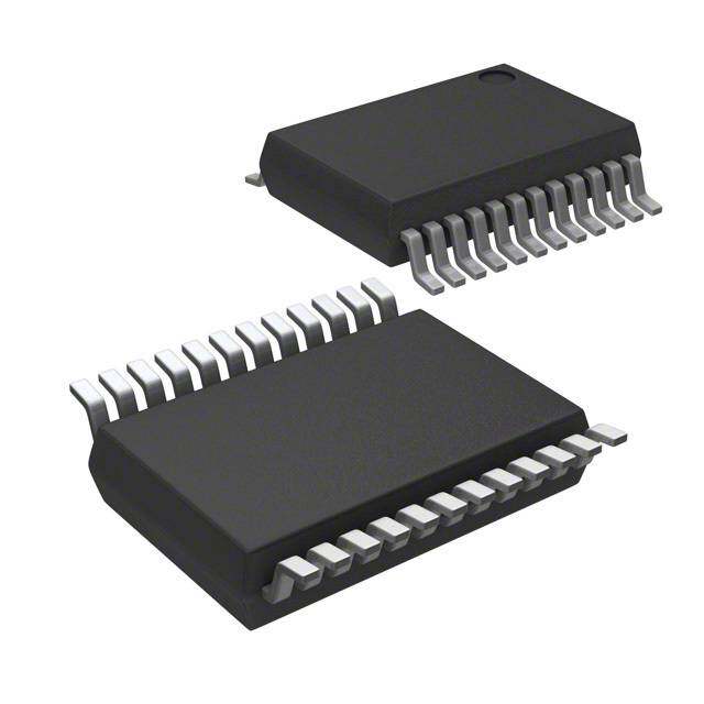
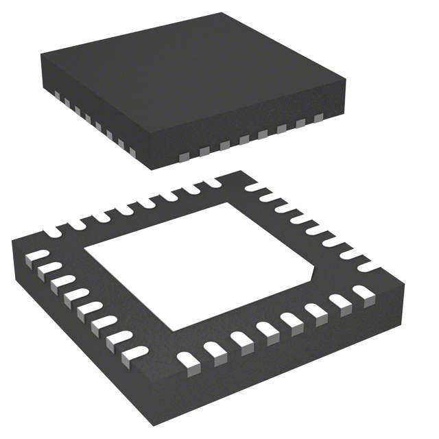
ICGOO电子元器件商城为您提供MAX2112ETI+由Maxim设计生产,在icgoo商城现货销售,并且可以通过原厂、代理商等渠道进行代购。 MAX2112ETI+价格参考¥60.69-¥99.54。MaximMAX2112ETI+封装/规格:RF 接收器, - RF Receiver 925MHz ~ 2.175GHz PCB, Surface Mount 28-TQFN (5x5)。您可以下载MAX2112ETI+参考资料、Datasheet数据手册功能说明书,资料中有MAX2112ETI+ 详细功能的应用电路图电压和使用方法及教程。
MAX2112ETI+是Maxim Integrated推出的一款高度集成的RF接收器,主要用于数字电视和无线通信系统。该器件广泛应用于DVB-T(地面数字视频广播)和ISDB-T(综合业务数字广播-地面)系统,适用于数字机顶盒、移动电视接收设备及便携式多媒体终端等场景。MAX2112ETI+集成了低噪声放大器(LNA)、混频器、本振(LO)合成器和中频处理电路,支持VHF和UHF频段信号接收,具备良好的灵敏度和抗干扰能力。其单芯片设计简化了外围电路,降低了系统成本与尺寸,特别适合对空间和功耗敏感的应用。此外,该器件采用紧凑的TQFN封装,便于在小型化设备中布局,广泛用于车载电视、手持式数字电视接收器以及家庭数字接收终端,为稳定接收高质量数字电视信号提供可靠解决方案。
| 参数 | 数值 |
| 产品目录 | |
| 描述 | IC TUNER DIR-CONV DVB-S2 28TQFN调谐器 Direct Conv Tuner Tuner for DVB-S2 |
| DevelopmentKit | MAX2112EVKIT+ |
| 产品分类 | |
| 品牌 | Maxim Integrated |
| 产品手册 | |
| 产品图片 |
|
| rohs | 符合RoHS无铅 / 符合限制有害物质指令(RoHS)规范要求 |
| 产品系列 | RF集成电路,调谐器,Maxim Integrated MAX2112ETI+- |
| 数据手册 | |
| 产品型号 | MAX2112ETI+ |
| 产品培训模块 | http://www.digikey.cn/PTM/IndividualPTM.page?site=cn&lang=zhs&ptm=25703http://www.digikey.cn/PTM/IndividualPTM.page?site=cn&lang=zhs&ptm=25705 |
| 产品种类 | 调谐器 |
| 供应商器件封装 | 28-TQFN (5x5) |
| 功能 | Satellite |
| 包装 | 管件 |
| 商标 | Maxim Integrated |
| 噪声系数 | 8 dB |
| 天线连接器 | PCB,表面贴装 |
| 存储容量 | - |
| 安装风格 | SMD/SMT |
| 封装 | Tube |
| 封装/外壳 | 28-WFQFN 裸露焊盘 |
| 封装/箱体 | QFNEP-28 |
| 工作温度 | -40°C ~ 85°C |
| 工作电源电压 | 3.3 V |
| 工厂包装数量 | 60 |
| 应用 | 数字 TV,CATV,机顶盒 |
| 应用说明 | |
| 总线类型 | 2-Wire, I2C |
| 数据接口 | PCB,表面贴装 |
| 数据速率(最大值) | - |
| 最大工作温度 | + 70 C |
| 最大频率 | 2175 MHz |
| 最小工作温度 | 0 C |
| 最小频率 | 925 MHz |
| 标准包装 | 1 |
| 灵敏度 | - |
| 特性 | - |
| 电压-电源 | 3.13 V ~ 3.47 V |
| 电流-接收 | 100mA |
| 电源电压-最大 | 3.47 V |
| 电源电压-最小 | 3.13 V |
| 电源电流 | 100 mA |
| 系列 | MAX2112 |
| 调制或协议 | - |
| 调制技术 | PSK |
| 零件号别名 | MAX2112 |
| 频率 | 925MHz ~ 2.175GHz |

.jpg)


- 商务部:美国ITC正式对集成电路等产品启动337调查
- 曝三星4nm工艺存在良率问题 高通将骁龙8 Gen1或转产台积电
- 太阳诱电将投资9.5亿元在常州建新厂生产MLCC 预计2023年完工
- 英特尔发布欧洲新工厂建设计划 深化IDM 2.0 战略
- 台积电先进制程称霸业界 有大客户加持明年业绩稳了
- 达到5530亿美元!SIA预计今年全球半导体销售额将创下新高
- 英特尔拟将自动驾驶子公司Mobileye上市 估值或超500亿美元
- 三星加码芯片和SET,合并消费电子和移动部门,撤换高东真等 CEO
- 三星电子宣布重大人事变动 还合并消费电子和移动部门
- 海关总署:前11个月进口集成电路产品价值2.52万亿元 增长14.8%


PDF Datasheet 数据手册内容提取
EVALUATION KIT AVAILABLE AVAILABLE MAX2112 Complete, Direct-Conversion Tuner for DVB-S2 Applications General Description Features The MAX2112 low-cost, direct-conversion tuner IC is (cid:1) 925MHz to 2175MHz Frequency Range designed for satellite set-top and VSAT applications. (cid:1) Monolithic VCO The IC is intended for 8PSK and Digital Video Low Phase Noise: -97dBc/Hz at 10kHz Broadcast (DVB-S2) applications. No Calibration Required The MAX2112 directly converts the satellite signals (cid:1) High Dynamic Range: -75dBm to 0dBm from the LNB to baseband using a broadband I/Q (cid:1) Integrated Variable BW LP Filters: 4MHz to 40MHz downconverter. The operating frequency range extends (cid:1) Single +3.3V ±5% Supply from 925MHz to 2175MHz. (cid:1) Low-Power Standby Mode The device includes an LNA and an RF variable-gain (cid:1) Address Pin for Multituner Applications amplifier, I and Q downconverting mixers, and baseband lowpass filters with programmable cutoff frequency control (cid:1) Differential I/Q Interface and digitally controlled baseband variable-gain amplifiers. (cid:1) I2C 2-Wire Serial Interface Together, the RF and baseband variable-gain amplifiers (cid:1) Very Small 28-Pin TQFN Package provide more than 80dB of gain control range. The IC is compatible with virtually all DVB-S2 demodulators. The MAX2112 includes fully monolithic VCOs, as well as Ordering Information a complete fractional-N frequency synthesizer. Additionally, an on-chip crystal oscillator is provided along with a buffered output for driving additional tuners PART TEMP RANGE PIN-PACKAGE and demodulators. Synthesizer programming and device MAX2112CTI+ 0°C to +70°C 28 Thin QFN-EP* configuration are accomplished with a 2-wire serialinter- MAX2112ETI+ -40°C to +85°C 28 Thin QFN-EP* face. The IC features a VCO autoselect (VAS) function *EP = Exposed paddle. that automatically selects the proper VCO. For multituner +Denotes a lead(Pb)-free/RoHS-compliant package. applications, the device can be configured to have one of two 2-wire interface addresses. A low-power standby mode is available whereupon the signal path is shut Pin Configuration/ down while leaving the reference oscillator, digital inter- Functional Diagram face, and buffer circuits active, providing a method to reduce power in single and multituner applications. Functional Diagrams The MAX2112 is the most advanced DBS tuner avail- BB able today. The low noise figureeliminates the need for ADDR SCL SDA VCC_ QDC- QDC+ IDC- an external LNA. A small number of passive compo- + 28 27 26 25 24 23 22 nents are needed to form a complete DVB-S2 RF front- end solution. The tuner is available in a very small VCC_RF2 1 INTERFACE LOGIC MAX2112 CDOCR ROEFCFTSIEOTN 21 IDC+ 28-pin thin QFN package. AND CONTROL LPF BW Applications VCC_RF1 2 CONTROL 20 IOUT- DirecTV and Dish Network DBS GND 3 19 IOUT+ DVB-S2 RFIN 4 18 QOUT- VSATs GC1 5 17 QOUT+ FREQUENCY DIV2/DIV4 SYNTHESIZER VCC_LO 6 16 VCC_DIG EP VCC_VCO 7 15 REFOUT 8 9 10 11 12 13 14 Pin Configurations appear at end of data sheet. FUuCnScPt iiosn aa tlr Dadiaegmraamrk so fc Monatxinimu eIndt eagt reantedd o Pf rdoadtuac stsh, eInect.. VCOBYP VTUNE GNDTUNE GNDSYN CPOUT VCC_SYN XTAL For pricing, delivery, and ordering information, please contact Maxim Direct at 1-888-629-4642, or visit Maxim’s website at www.maximintegrated.com. 19-0869; Rev 2; 5/10
MAX2112 Complete, Direct-Conversion Tuner for DVB-S2 Applications ABSOLUTE MAXIMUM RATINGS VCCto GND...........................................................-0.3V to +3.9V Operating Temperature Range (MAX2112CTI+)......0°C to +70°C All Other Pins to GND.................................-0.3V to (VCC+ 0.3V) Operating Temperature Range (MAX2112ETI+)...-40°C to +85°C RF Input Power: RFIN.....................................................+10dBm Junction Temperature......................................................+150°C VCOBYP, CPOUT, XTAL, REFOUT, IOUT_, QOUT_ , IDC_, Storage Temperature Range.............................-65°C to +160°C QDC_ to GND Short-Circuit Protection...............................10s Lead Temperature (soldering, 10s).................................+300°C Continuous Power Dissipation (TA= +70°C) Soldering Temperature (reflow).......................................+260°C 28-Pin Thin QFN (derated 34.5mW/°C above +70°C)...2.75W Stresses beyond those listed under “Absolute Maximum Ratings” may cause permanent damage to the device. These are stress ratings only, and functional operation of the device at these or any other conditions beyond those indicated in the operational sections of the specifications is not implied. Exposure to absolute maximum rating conditions for extended periods may affect device reliability. CAUTION! ESD SENSITIVE DEVICE DC ELECTRICAL CHARACTERISTICS (MAX2112 Evaluation Kit: VCC = +3.13V to +3.47V, TA= 0°C to +70°C (MAX2112CTI+), TA= -40°C to +85°C (MAX2112ETI+), VGC1 = +0.5V (max gain), default register settings except BBG[3:0] = 1011. No input signals at RF, baseband I/Os are open circuited. Typical values measured at VCC= +3.3V, TA= +25°C.) (Note 1) PARAMETER CONDITIONS MIN TYP MAX UNITS SUPPLY Supply Voltage 3.13 3.3 3.47 V Receive mode, bit STBY = 0 100 160 Supply Current mA Standby mode, bit STBY = 1 3 ADDRESS SELECT INPUT (ADDR) Digital Input Voltage High, VIH 2.4 V Digital Input Voltage Low, VIL 0.5 V Digital Input Current High, IIH 50 µA Digital Input Current Low, IIL -50 µA ANALOG GAIN-CONTROL INPUT (GC1) Input Voltage Range Maximum gain = 0.5V 0.5 2.7 V Input Bias Current -50 +50 µA VCO TUNING VOLTAGE INPUT (VTUNE) Input Voltage Range 0.4 2.3 V 2-WIRE SERIAL INPUTS (SCL, SDA) Clock Frequency 400 kHz 0.7 x Input Logic-Level High V VCC 0.3 x Input Logic-Level Low V VCC Input Leakage Current Digital inputs = GND or VCC ±0.1 ±1 µA 2-WIRE SERIAL OUTPUT (SDA) Output Logic-Level Low ISINK = 1mA 0.4 V 2 Maxim Integrated
MAX2112 Complete, Direct-Conversion Tuner for DVB-S2 Applications AC ELECTRICAL CHARACTERISTICS (MAX2112 Evaluation Kit: VCC = +3.13V to +3.47V, TA= 0°C to +70°C (MAX2112CTI+), TA= -40°C to +85°C (MAX2112ETI+), default register settings except BBG[3:0] = 1011. Typical values measured at VCC= +3.3V, TA= +25°C.) (Note 1) PARAMETER CONDITIONS MIN TYP MAX UNITS MAIN SIGNAL PATH PERFORMANCE Input Frequency Range (Note 2) 925 2175 MHz RF Gain-Control Range (GC1) 0.5V < VGC1 < 2.7V 65 73 dB Baseband Gain-Control Range Bits GC2 = 1111 to 0000 13 15 dB In-Band Input IP3 (Note 3) +2 dBm Out-of-Band Input IP3 (Note 4) +15 dBm Input IP2 (Note 5) +40 dBm Adjacent Channel Protection (Note 6) 25 dB VGC1 is set to 0.5V (maximum RF gain) and BBG[3:0] is adjusted to give a 1VP-P baseband output level for a 8 Noise Figure -75dBm CW input tone at 1500MHz dB Starting with the same BBG[3:0] setting as above, VGC1 9 12 is adjusted to back off RF gain by 10dB (Note 7) Minimum RF Input Return Loss 925MHz < fRF < 2175MHz, in 75Ω system 12 dB BASEBAND OUTPUT CHARACTERISTICS Nominal Output Voltage Swing RLOAD = 2kΩ//10pF 0.5 1 VP-P I/Q Amplitude Imbalance Measured at 500kHz; filter set to 22.27MHz ±1 dB I/Q Quadrature Phase Imbalance Measured at 500kHz; filter set to 22.27MHz 3.5 De g re es Si n gl e -E n de d I/Q Outp ut Imp eda nce Real ZO, from 1MHz to 40MHz 30 Ω Output 1dB Compression Voltage Differential 3 VP-P Baseband Highpass -3dB 47nF capacitors at IDC_, QDC_ 400 Hz Frequency Corner BASEBAND LOWPASS FILTERS Filter Bandwidth Range 4 40 MHz Rejection Ratio At 2 x f-3dB 39 dB Group Delay Up to 1dB bandwidth 37 ns Ratio of In-Filter-Band to Out-of- fINBAND = 100Hz to 22.5MHz, fOUTBAND = 87.5MHz to 25 dB Filter-Band Noise 112.5MHz FREQUENCY SYNTHESIZER RF-Divider Frequency Range 925 2175 MHz RF-Divider Range (N) 19 251 Refere nce-D i v id er Fre qu ency Range 12 30 MHz Reference-Divider Range (R) 1 1 Phase-Detector Comparison 12 30 MHz Frequency VOLTAGE-CONTROLLED OSCILLATOR AND LO GENERATION Guaranteed LO Frequency Range 925 2175 MHz fOFFSET = 10kHz -97 LO Phase Noise fOFFSET = 100kHz -100 dBc/Hz fOFFSET = 1MHz -122 Maxim Integrated 3
MAX2112 Complete, Direct-Conversion Tuner for DVB-S2 Applications AC ELECTRICAL CHARACTERISTICS (continued) (MAX2112 Evaluation Kit: VCC = +3.13V to +3.47V, TA= 0°C to +70°C (MAX2112CTI+), TA= -40°C to +85°C (MAX2112ETI+), default register settings except BBG[3:0] = 1011. Typical values measured at VCC= +3.3V, TA= +25°C.) (Note 1) PARAMETER CONDITIONS MIN TYP MAX UNITS XTAL/REFERENCE OSCILLATOR INPUT AND OUTPUT BUFFER XTAL Oscillator Frequency Range Parallel-resonance-mode crystal (Note 8) 12 30 MHz Input Overdrive level AC-coupled sine-wave input 0.5 1 2.0 VP-P XTAL Output-Buffer Divider Range 1 8 XTAL Output Voltage Swing 4MHz to 30MHz, CLOAD = 10pF 1 1.5 2 VP-P XTAL Output Duty Cycle 50 % Note 1:MAX2112CTI+: Min/max values are production tested at TA= +70°C. Min/max limits at TA= 0°C and TA= +25°C are guaranteed by design and characterization. MAX2112ETI+: Min/max values are production tested at TA= +85°C. Min/max limits at TA= -40°C and TA= +25°C are guaranteed by design and characterization. Note 2:Input gain range specifications met over this band. Note 3:In-band IIP3 test conditions: GC1 set to provide the nominal baseband output drive when mixing down a -23dBm tone at 2175MHz to 5MHz baseband (fLO= 2170MHz). Baseband gain is set to its default value (BBG[3:0] = 1011). Two tones at -26dBm each are applied at 2174MHz and 2175MHz. The IM3 tone at 3MHz is measured at baseband, but is referred to the RF input. Note 4:Out-of-band IIP3 test conditions: GC1 set to provide nominal baseband output drive when mixing down a -23dBm tone at 2175MHz to 5MHz baseband (fLO= 2170MHz). Baseband gain is set to its default value (BBG[3:0] = 1011). Two tones at -20dBm each are applied at 2070MHz and 1975MHz. The IM3 tone at 5MHz is measured at baseband, but is referred to the RF input. Note 5:Input IP2 test conditions: GC1 set to provide nominal baseband output drive when mixing down a -23dBm tone at 2175MHz to 5MHz baseband (fLO= 2170MHz). Baseband gain is set to its default value (BBG[3:0] = 1011). Two tones at -20dBm each are applied at 925MHz and 1250MHz. The IM2 tone at 5MHz is measured at baseband, but is referred to the RF input. Note 6:Adjacent channel protection test conditions: GC1 is set to provide the nominal baseband output drive with a 2110MHz 27.5Mbaud signal at -55dBm. GC2 set for mid-scale. The test signal shall be set for PR = 7/8 and SNR of -8.5dB. An adja- cent channel at ±40MHz is added at -25dBm. DVB-S BER performance of 2E-4 shall be maintained for the desired signal. GC2 may be adjusted for best performance. Note 7:Guaranteed by design and characterization at TA= +25°C. Note 8:See Table 16 for crystal ESR requirements. 4 Maxim Integrated
MAX2112 Complete, Direct-Conversion Tuner for DVB-S2 Applications Typical Operating Characteristics (MAX2112 Evaluation Kit: VCC = +3.3V, TA = +25°C, baseband output frequency = 5MHz; VGC1 = +1.2V, default register settings except BBG[3:0] = 1011.) STANDBY MODE SUPPLY CURRENT SUPPLY CURRENT SUPPLY CURRENT vs. SUPPLY VOLTAGE vs. SUPPLY VOLTAGE vs. BASEBAND FILTER CUTOFF FREQUENCY 999678 TA = +85°C MAX2112 toc01 23..90 TA = +85°C MAX2112 toc02 111000024 MAX2112 toc03 SUPPLY CURRENT (mA) 9999912345 TTAA == +-4205°°CC SUPPLY CURRENT (mA) 2222....5678 TA = +25°C SUPPLY CURRENT (mA) 9999902468 90 88 2.4 TA = -40°C 89 86 88 2.3 84 3.0 3.1 3.2 3.3 3.4 3.5 3.6 3.0 3.1 3.2 3.3 3.4 3.5 3.6 4 8 12 16 20 24 28 32 36 40 SUPPLY VOLTAGE (V) SUPPLY VOLTAGE (V) BASEBAND FILTER CUTOFF FREQUENCY (MHz) QUADRATURE MAGNITUDE MATCHING HD3 vs. VOUT QUADRATURE PHASE vs. LO FREQUENCY vs. LO FREQUENCY -10 93.5 1.0 BASEBAND 3RD-ORDER HARMONIC (dBc) ---------554433221505050505 MAX2112 toc04 °QUADRATURE PHASE ()888999789012......555555 fBASEBANTDA == 1+02TM5A°H =Cz -40°C TA = +85°C MAX2112 toc05a QUADRATURE MAGNITUDE MATCHING (dB) ----00000000........642204688 fBASEBAND = 1T0ATM A= H =+ z2-450°°CC TA = +85°C MAX2112 toc05b -60 86.5 -1.0 1.0 1.5 2.0 2.5 3.0 3.5 900 1200 1500 1800 2100 2400 900 1200 1500 1800 2100 2400 VOUT (VP-P) LO FREQUENCY (MHz) LO FREQUENCY (MHz) QUADRATURE PHASE QUADRATURE MAGNITUDE MATCHING BASEBAND FILTER vs. BASEBAND FREQUENCY vs. BASEBAND FREQUENCY FREQUENCY RESPONSE °ADRATURE PHASE () 8999990123.....55555 fLO = 925MHz TA = T+A2 5=° C+85°TCA = -40°C MAX2112 toc06a E MAGNITUDE MATCHING (dB) -000001......2204680 fLO = 925MHz TA = +85°C MAX2112 toc06b AND OUTPUT LEVEL (dB) -----53421000000 MAX2112 toc07 QU 88.5 RATUR --00..64 TA = +25°C TA = -40°C BASEB -60 D 87.5 QUA -0.8 -70 86.5 -1.0 -80 0 4 8 12 16 20 0 4 8 12 16 20 0 20 40 60 80 BASEBAND FREQUENCY (MHz) BASEBAND FREQUENCY (MHz) BASEBAND FREQUENCY (MHz) Maxim Integrated 5
MAX2112 Complete, Direct-Conversion Tuner for DVB-S2 Applications Typical Operating Characteristics (continued) (MAX2112 Evaluation Kit: VCC = +3.3V, TA = +25°C, baseband output frequency = 5MHz; VGC1 = +1.2V, default register settings except BBG[3:0] = 1011.) BASEBAND FILTER HIGHPASS PROGRAMMED f-3dB FREQUENCY BASEBAND FILTER 3dB FREQUENCY FREQUENCY RESPONSE vs. MEASURED f-3dB FREQUENCY vs. TEMPERATURE BASEBAND OUTPUT LEVEL (dB) -1----8462020 MAX2112 toc08 MEASURED f FREQUENCY (MHz)-3dB 1212334400555005 LPF[7:0] = 12 + (f-3dB - 4MHz)/290kHz MAX2112 toc09 ASEBAND GAIN ERROR AT f (dB)-3dB---00000001........642024680 NORMALIZED TO TA = +25°C MAX2112 toc10 -12 5 B -0.8 -14 0 -1.0 100 1000 10,000 0 5 10 15 20 25 30 35 40 45 -40 -20 0 20 40 60 80 BASEBAND FREQUENCY (MHz) PROGRAMMED f-3dB FREQUENCY (MHz) TEMPERATURE (°C) INPUT POWER vs. VGC1 NOISE FIGURE vs. FREQUENCY NOISE FIGURE vs. INPUT POWER 10 10.5 70 -100 AOPIDUNJT =UP S-U7TT5 BdWBBIGmTH[ 3A:N0]D F VOGRC 11 V=P 0-P.5 BVASEBAND MAX2112 toc11 10.0 OAADNUJDTUP VSUGTTC B1W B=IGT 0H[.35 P:V0I]N F=O -R7 51dVBPm-P BASEBAND MAX2112 toc12 60 fABPLDAIONS J ==UE 1BS-75AT50N Bd0DBBM GmOH[U z3AT:N0P]DU F TVO GWRC I11T V=HP 0-P.5V. MAX2112 toc13 INPUT POWER (dBm) ----54320000 TA = -40°C TA = T+A8 5=° +C25°C NOISE FIGURE (dB) 899...505 TA = +7T0A° C= +85°C NOISE FIGURE (dB) 23450000 -60 8.0 TA = +25°C 10 -70 -80 7.5 0 0.5 1.0 1.5 2.0 2.5 3.0 900 1100 1300 1500 1700 1900 2100 2300 -80 -70 -60 -50 -40 -30 -20 -10 0 VGC1 (V) FREQUENCY (MHz) INPUT POWER (dBm) OUT-OF-BAND IIP3 vs. INPUT POWER IN-BAND IIP3 vs. INPUT POWER IIP2 vs. INPUT POWER 30 30 60 20 SEE NOTE 4 ON PAGE 4 FOR CONDITIONS MAX2112 toc14 1200 SEE NOTE 3 ON PAGE 4 FOR CONDITIONS MAX2112 toc15 50 SEE NOTE 5 ON PAGE 4 FOR CONDITIONS MAX2112 toc16 OUT-OF-BAND IIP3 (dBm) -11000 IN-BAND IIP3 (dBm) ---3120000 IIP2 (dBm) 13240000 -40 -20 0 -50 -30 -60 -10 -80 -70 -60 -50 -40 -30 -20 -10 0 -80 -70 -60 -50 -40 -30 -20 -10 0 -80 -70 -60 -50 -40 -30 -20 -10 0 INPUT POWER (dBm) INPUT POWER (dBm) INPUT POWER (dBm) 6 Maxim Integrated
MAX2112 Complete, Direct-Conversion Tuner for DVB-S2 Applications Typical Operating Characteristics (continued) (MAX2112 Evaluation Kit: VCC = +3.3V, TA = +25°C, baseband output frequency = 5MHz; VGC1 = +1.2V, default register settings except BBG[3:0] = 1011.) INPUT RETURN LOSS vs. FREQUENCY PHASE NOISE AT 10kHz OFFSET vs. 0 CHANNEL FREQUENCY RN LOSS (dB) -1-50 VGC1 = 0.5V MAX2112 toc17 OFFSET (dBc/Hz) --9950 MAX2112 toc18 UT RETU -15 T 10kHz P A IN SE -100 -20 OI N E S -25 VGC1 = 2.7V PHA 900 1125 1350 1575 1800 2025 2250 -105 FREQUENCY (MHz) 925 1115 1305 1495 1685 1875 2065 2255 CHANNEL FREQUENCY (MHz) PHASE NOISE vs. OFFSET FREQUENCY LO LEAKAGE vs. LO FREQUENCY -90 -70 MAX2112 toc19 MEASURED AT RF INPUT MAX2112 toc20 -100 -75 Bc/Hz) Bm) PHASE NOISE (d-110 LO LEAKAGE (d -80 -120 -85 fLO = 1800MHz -130 -90 1.0E+03 1.0E+04 1.0E+05 1.0E+06 925 1175 1425 1675 1925 2175 OFFSET FREQUENCY (Hz) LO FREQUENCY (MHz) VCO: KV vs. VTUNE 450 345000 SUB-BAND 23 MAX2112 toc21 300 Hz/V) 250 M V ( 200 SUB-BAND 12 K 150 100 50 SUB-BAND 0 0 0 0.5 1.0 1.5 2.0 2.5 3.0 VTUNE (V) Maxim Integrated 7
MAX2112 Complete, Direct-Conversion Tuner for DVB-S2 Applications Pin Description PIN NAME FUNCTION DC Power Supply for LNA. Connect to a +3.3V low-noise supply. Bypass to GND with a 1nF capacitor 1 VCC_RF2 connected as close as possibl e to the pin . Do not share capacit or gro und via s wi th other gr o und connections. DC Power Supply for LNA. Connect to a +3.3V low-noise supply. Bypass to GND with a 1nF capacitor 2 VCC_RF1 connected as close as possibl e to the pin . Do not share capacit or gro und via s wi th other gr o und connections. 3 GND Ground. Connect to board’s ground plane for proper operation. 4 RFIN Wideband 75Ω RF Input. Connect to an RF source through a DC-blocking capacitor. RF Gain-Control Input. High-impedance analog input with a 0.5V to 2.7V operating range. 5 GC1 VGC1 = 0.5V corresponds to the maximum gain setting. DC Power Supply for LO Generation Circuits. Connect to a +3.3V low-noise supply. Bypass to GND with 6 VCC_LO a 1nF capacitor connected as close as possible to the pin. Do not share capacitor ground vias with other ground connections. DC Power Supply for VCO Circuits. Connect to a +3.3V low-noise supply. Bypass to GND with a 1nF 7 VCC_VCO capacitor connected as close as possible to the pin. Do not share capacitor ground vias with other ground connections. Internal VCO Bias Bypass. Bypass to GND with a 100nF capacitor connected as close as possible to 8 VCOBYP the pin. Do not share capacitor ground vias with other ground connections. High-Impedance VCO Tune Input. Connect the PLL loop filter output directly to this pin with as short of a 9 VTUNE connection as possible. 10 GNDTUNE Ground for VTUNE. Connect to the PCB ground plane. 11 GNDSYN Ground for Synthesizer. Connect to the PCB ground plane. C h ar g e - P um p O u tp u t . C o n n e c t t h i s o u t p u t t o t he P L L l o o p fi l t e r i n p u t w i t h th e s h or t e s t c o n n e ct i o n 12 CPOUT p o ss i b l e . DC Power Supply for Synthesizer Circuits. Connect to a +3.3V low-noise supply. Bypass to GND with a 13 VCC_SYN 1nF capacitor connected as close as possible to the pin. Do not share capacitor ground vias with other ground connections. Crystal-Oscillator Interface. Use with an external parallel-resonance-mode crystal through a series 1nF 14 XTAL capacitor. See the Typical Application Circuit. 15 REFOUT Crystal-Oscillator Buffer Output. A DC-blocking capacitor must be used when driving external circuitry. DC Power Supply for Digital Logic Circuits. Connect to a +3.3V low-noise supply. Bypass to GND with a 16 VCC_DIG 1nF capacitor connected as close as possible to the pin. Do not share capacitor ground vias with other ground connections. 17 QOUT+ Quadrature Baseband Differential Output. AC-couple with 47nF capacitors to the demodulator input. 18 QOUT- 19 IOUT+ In-Phase Baseband Differential Output. AC-couple with 47nF capacitors to the demodulator input. 20 IOUT- 21 IDC+ I-Channel Baseband DC Offset Correction. Connect a 47nF ceramic chip capacitor from IDC- to IDC+. 22 IDC- 23 QDC+ Q-C h annel Baseb and D C Of fset Co rr e ctio n. C onnect a 47nF cera mi c chip capa cit or fro m QDC - to QDC + . 24 QDC- DC Power Supply for Baseband Circuits. Connect to a +3.3V low-noise supply. Bypass to GND with 25 VCC_BB a 1nF capacitor connected as close as possible to the pin. Do not share capacitor ground vias with other ground connections. 8 Maxim Integrated
MAX2112 Complete, Direct-Conversion Tuner for DVB-S2 Applications Pin Description (continued) PIN NAME FUNCTION 26 SDA 2-Wire Serial-Data Interface. Requires ≥ 1kΩ pullup resistor to VCC. 27 SCL 2-Wire Serial-Clock Interface. Requires ≥ 1kΩ pullup resistor to VCC. 28 ADDR Address. Must be connected to either ground (logic 0) or supply (logic 1). — EP Exposed Paddle. Solder evenly to the board’s ground plane for proper operation. Detailed Description configurations. The register configuration of Table 1 shows each bit name and the bit usage information for all Register Description registers. Note that all registers must be written after and The MAX2112 includes 12 user-programmable regis- no earlier than 100µs after the device is powered up. ters and 2 read-only registers. See Table 1 for register Table 1. Register Configuration MSB LSB REG RE GI STE R RE AD / RE G DATA BYTE NUMBER NA ME WR IT E AD DR ESS D[7] D[6] D[5] D[4] D[3] D[2] D[1] D[0] N-Divider FRAC 1 Write 0x00 N[14] N[13] N[12] N[11] N[10] N[9] N[8] MSB 1 N-Divider 2 Write 0x01 N[7] N[6] N[5] N[4] N[3] N[2] N[1] N[0] LSB Charge CPMP[1] CPMP[0] CPLIN[1] CPLIN[0] 3 Write 0x02 F[19] F[18] F[17] F[16] Pump 0 0 0 1 F-Divider 4 Write 0x03 F[15] F[14] F[13] F[12] F[11] F[10] F[9] F[8] MSB F-Divider 5 Write 0x04 F[7] F[6] F[5] F[4] F[3] F[2] F[1] F[0] LSB XTAL 6 Divider Write 0x05 XD[2] XD[1] XD[0] R[4] R[3] R[2] R[1] R[0] R-Divider 7 PLL Write 0x06 D24 CPS ICP X X X X X 8 VCO Write 0x07 VCO[4] VCO[3] VCO[2] VCO[1] VCO[0] VAS ADL ADE 9 LPF Write 0x08 LPF[7] LPF[6] LPF[5] LPF[4] LPF[3] LPF[2] LPF [1 ] LPF[0] PWDN 10 Control Write 0x09 STBY X X BBG[3] BBG[2 ] BBG[1 ] BBG[0 ] 0 PLL DIV VCO BB RFMIX RFVGA FE 11 Shutdown Write 0x0A X 0 0 0 0 0 0 0 LD LD LD CPTST[2] CPTST[1] CPTST[0] TURBO 12 Test Write 0x0B X MU X [2 ] MU X [1 ] MU X [0 ] 0 0 0 1 0 0 0 Status 13 Read 0x0C POR VASA VASE LD X X X X Byte-1 Status 14 Read 0x0D VC O SB R[4] VC O SB R[3] VC O SB R[2] VC O SB R[1] VC O SB R[0] ADC [2 ] ADC [1 ] ADC [0 ] Byte-2 X = Don’t care. 0 = Set to 0 for factory-tested operation. 1 = Set to 1 for factory-tested operation. Maxim Integrated 9
MAX2112 Complete, Direct-Conversion Tuner for DVB-S2 Applications Table 2. N-Divider MSB Register BIT NAME BIT LOCATION (0 = LSB) DEFAULT FUNCTION FRAC 7 1 Users must program to 1 upon powering up the device. Sets the most significant bits of the PLL integer-divide number (N). N can N[14:8] 6–0 0000000 range from 19 to 251. Table 3. N-Divider LSB Register BIT NAME BIT LOCATION (0 = LSB) DEFAULT FUNCTION Sets the least significant bits of the PLL integer-divide number. N can range N[7:0] 7–0 00100011 from 19 to 251. Table 4. Charge-Pump Register BIT NAME BIT LOCATION (0 = LSB) DEFAULT FUNCTION Charge-pump minimum pulse width. Users must program to 00 upon CPMP[1:0] 7–6 00 powering up the device. Controls charge-pump linearity. Users must program to 01 upon powering up CPLIN[1:0] 5–4 00 the device. Se ts the 4 mo st sig n if ic ant bi t s of the PL L fra ctio nal di vid e numb e r. F[19:16] 3–0 0010 De fault valu e i s F = 194,180 de cim a l. Table 5. F-Divider MSB Register BIT NAME BIT LOCATION (0 = LSB) DEFAULT FUNCTION Se ts the mo st sig n if i cant bi t s of the PL L fra ctio nal- d i v id e num be r (F ). F[15:8] 7–0 11110110 De fault valu e i s F = 194,180 de cim a l. Table 6. F-Divider LSB Register BIT NAME BIT LOCATION (0 = LSB) DEFAULT FUNCTION Se ts the le ast sig n if ic ant bi t s of the PL L fra ctio nal- d i v id e numb e r (F ). F[7:0] 7–0 10000100 De fault valu e i s F = 194,180 de cim a l. Table 7. XTAL Buffer and Reference Divider Register BIT NAME BIT LOCATION (0 = LSB) DEFAULT FUNCTION Sets the crystal-divider setting. 000 = Divide by 1. 001 = Divide by 2. XD[2:0] 7–5 000 011 = Divide by 3. 100 = Divide by 4. 101 through 110 = All divide values from 5 (101) to 7 (110). 111 = Divide by 8. Sets the PLL reference-divider (R) number. Users must program to 00001 R[4:0] 4–0 00001 upon powering up the device. 00001 = Divide by 1; other values are not tested. 10 Maxim Integrated
MAX2112 Complete, Direct-Conversion Tuner for DVB-S2 Applications Table 8. PLL Register BIT NAME BIT LOCATION (0 = LSB) DEFAULT FUNCTION VCO divider setting. D24 7 1 0 = Divide by 2. Use for LO frequencies ≥ 1125MHz. 1 = Divide by 4. Use for LO frequencies < 1125MHz. Charge-pump current mode. CPS 6 1 0 = Charge-pump current controlled by ICP bit. 1 = Charge-pump current controlled by VCO autoselect (VAS). Charge-pump current. ICP 5 0 0 = 600µA typical. 1 = 1200µA typical. X 4–0 X Don’t care. Table 9. VCO Register BIT NAME BIT LOCATION (0 = LSB) DEFAULT FUNCTION Co ntro ls w hic h VC O is acti vated wh en usin g m anual VC O p ro g ra mm i ng mo de . VCO[4:0] 7–3 11001 This al so serv es as the star tin g po in t for the VC O autosel ectio n ( VA S) mo d e. VCO autoselection (VAS) circuit. VAS 2 1 0 = Disable VCO selection must be programmed through I2C. 1 = Enable VCO selection controlled by autoselection circuit. Enables or disables the VCO tuning voltage ADC latch when the VCO autoselect mode (VAS) is disabled. ADL 1 0 0 = Disables the ADC latch. 1 = Latches the ADC value. Enables or disables VCO tuning voltage ADC read when the VCO autoselect mode (VAS) is disabled. ADE 0 0 0 = Disables ADC read. 1 = Enables ADC read. Table 10. Lowpass Filter Register BIT NAME BIT LOCATION (0 = LSB) DEFAULT FUNCTION Sets the baseband lowpass filter 3dB corner frequency. LPF[7:0] 7–0 01001011 f-3dB = 4MHz + (LPF[7:0]dec - 12) x 290kHz. Default value equates to f-3dB = 22.27MHz typical. Maxim Integrated 11
MAX2112 Complete, Direct-Conversion Tuner for DVB-S2 Applications Table 11. Control Register BIT NAME BIT LOCATION (0 = LSB) DEFAULT FUNCTION Software standby control. 0 = Normal operation. STBY 7 0 1 = D is abl es the sig nal pa th and fre qu ency synthesi zer l eavi ng only the 2-w i r e b us, cry stal oscil l a tor, XT ALOU T b uffer , and XT ALOU T bu ffer d iv id er activ e. X 6 X Don’t care. Factory use only. PWDN 5 0 0 = Normal operation; other value is not tested. X 4 X Don’t care. Baseband gain setting (1dB typical per step). 0000 = Minimum gain (0dB, default). BBG[3:0] 3-0 0000 … 1111 = Maximum gain (15dB typical). Table 12. Shutdown Register BIT NAME BIT LOCATION (0 = LSB) DEFAULT FUNCTION X 7 X Don’t care. PLL enable. PLL 6 0 0 = Normal operation. 1 = Shuts down the PLL. Value not tested. Divider enable. DIV 5 0 0 = Normal operation. 1 = Shuts down the divider. Value not tested. VCO enable. VCO 4 0 0 = Normal operation. 1 = Shuts down the VCO. Value not tested. Baseband enable. BB 3 0 0 = Normal operation. 1 = Shuts down the baseband. Value not tested. RF mixer enable. RFMIX 2 0 0 = Normal operation. 1 = Shuts down the RF mixer. Value not tested. RF VGA enable. RFVGA 1 0 0 = Normal operation. 1 = Shuts down the RF VGA. Value not tested. Front-end enable. FE 0 0 0 = Normal operation. 1 = Shuts down the front-end. Value not tested. 12 Maxim Integrated
MAX2112 Complete, Direct-Conversion Tuner for DVB-S2 Applications Table 13. Test Register BIT NAME BIT LOCATION (0 = LSB) DEFAULT FUNCTION Charge-pump test modes. CPTST[2:0] 7–5 000 000 = Normal operation (default). X 4 X Don’t care. Charge-pump fast lock. TURBO 3 0 Users must program to 1 after powering up the device. REFOUT output. LDMUX[2:0] 2–0 000 000 = Normal operation. Other values are not tested. Table 14. Status Byte-1 Register BIT NAME BIT LOCATION (0 = LSB) FUNCTION Power-on reset status. 0 = Chip status register has been read with a stop condition since last power-on. POR 7 1 = Power-on reset (power cycle) has occurred. Default values have been loaded in registers. Indicates whether VCO autoselection was successful. VASA 6 0 = Indicates the autoselect function is disabled or unsuccessful VCO selection. 1 = Indicates successful VCO autoselection. Status indicator for the autoselect function. VASE 5 0 = Indicates the autoselect function is active. 1 = Indicates the autoselect process is inactive. PLL lock detector. TURBO bit must be programmed to 1 for valid LD reading. LD 4 0 = Unlocked. 1 = Locked. X 3:0 Don’t care. Table 15. Status Byte-2 Register BIT NAME BIT LOCATION (0 = LSB) FUNCTION VCOSBR[4:0] 7-3 VCO band readback. VAS ADC output readback. 000 = Out of lock. 001 = Locked. ADC[2:0] 2-0 010 = VAS locked. 101 = VAS locked. 110 = Locked. 111 = Out of lock. Maxim Integrated 13
MAX2112 Complete, Direct-Conversion Tuner for DVB-S2 Applications 2-Wire Serial Interface Slave Address The MAX2112 uses a 2-wire I2C-compatible serial inter- The MAX2112 has a 7-bit slave address that must be face consisting of a serial-data line (SDA) and a serial- sent to the device following a START condition to initi- clock line (SCL). SDA and SCL facilitate bidirectional ate communication. The slave address is internally pro- communication between the MAX2112 and the master grammed to 1100000. The eighth bit (R/W) following at clock frequencies up to 400kHz. The master initiates the 7-bit address determines whether a read or write a data transfer on the bus and generates the SCL sig- operation occurs. nal to permit data transfer. The MAX2112 behaves as a The MAX2112 continuously awaits a START condition slave device that transfers and receives data to and followed by its slave address. When the device recog- from the master. SDA and SCL must be pulled high nizes its slave address, it acknowledges by pulling the with external pullup resistors (1kΩor greater) for proper SDA line low for one clock period; it is ready to accept bus operation. Pullup resistors should be referenced to or send data depending on the R/Wbit (Figure1). the MAX2112’s VCC. The write/read address is C0/C1 if ADDR pin is con- One bit is transferred during each SCL clock cycle. A nected to ground. The write/read address is C2/C3 if minimum of nine clock cycles is required to transfer a ADDR pin is connected to VCC. byte in or out of the MAX2112 (8 bits and an ACK/NACK). The data on SDA must remain stable during the high period of the SCL clock pulse. Changes in SDA while SLAVE ADDRESS SCL is high and stable are considered control signals S 1 1 0 0 0 0 0 (see the START and STOP Conditionssection). Both SDA R/W ACK and SCL remain high when the bus is not busy. SDA START and STOP Conditions SCL 1 2 3 4 5 6 7 8 9 The master initiates a transmission with a START condi- tion (S), which is a high-to-low transition on SDA while Figure 1. MAX2112 Slave Address Byte with ADDR Pin SCL is high. The master terminates a transmission with Connected to Ground a STOP condition (P), which is a low-to-high transition on SDA while SCL is high. Write Cycle When addressed with a write command, the MAX2112 Acknowledge and Not-Acknowledge Conditions allows the master to write to a single register or to multi- Data transfers are framed with an acknowledge bit ple successive registers. (ACK) or a not-acknowledge bit (NACK). Both the mas- A write cycle begins with the bus master issuing a ter and the MAX2112 (slave) generate acknowledge START condition followed by the seven slave address bits. To generate an acknowledge, the receiving device bits and a write bit (R/W = 0). The MAX2112 issues an must pull SDA low before the rising edge of the ACK if the slave address byte is successfully received. acknowledge-related clock pulse (ninth pulse) and The bus master must then send to the slave the address keep it low during the high period of the clock pulse. of the first register it wishes to write to (see Table 1 for To generate a not-acknowledge condition, the receiver register addresses). If the slave acknowledges the allows SDA to be pulled high before the rising edge of address, the master can then write one byte to the regis- the acknowledge-related clock pulse, and leaves SDA ter at the specified address. Data is written beginning high during the high period of the clock pulse. with the most significant bit. The MAX2112 again issues Monitoring the acknowledge bits allows for detection of an ACK if the data is successfully written to the register. unsuccessful data transfers. An unsuccessful data The master can continue to write data to the successive transfer happens if a receiving device is busy or if a internal registers with the MAX2112 acknowledging each system fault has occurred. In the event of an unsuc- successful transfer, or it can terminate transmission by cessful data transfer, the bus master must reattempt issuing a STOP condition. The write cycle does not termi- communication at a later time. nate until the master issues a STOP condition. WRITE DEVICE WRITE REGISTER WRITE DATA TO WRITE DATA TO WRITE DATA TO R/W ACK ACK ACK ACK ACK START ADDRESS ADDRESS REGISTER 0x00 REGISTER 0x01 REGISTER 0x02 STOP 1100000 0 — 0x00 — 0x0E — 0xD8 — 0xE1 — Figure 2. Example: Write Registers 0 through 2 with 0x0E, 0xD8, and 0xE1, respectively. 14 Maxim Integrated
MAX2112 Complete, Direct-Conversion Tuner for DVB-S2 Applications ST ADDEDVRIECSES R / W A RAEDGDIRSETSESR A ST ADDEDVRIECSES R / W A RDEAGT 0A0 A RDEAGT 0A1 A RDEAGT 0A2 NA ST A C C A C C C C O R 1100000 0 K 00000000 K R 1100000 1 K xxxxxxxx K xxxxxxxx K xxxxxxxx K P T T Figure 3. Example: Receive Data from Read Registers Read Cycle Table 16. Maximum Crystal ESR When addressed with a read command, the MAX2112 Requirement allows the master to read back a single register, or mul- tiple successive registers. ESRMAX ((cid:2)) XTAL FREQUENCY (MHz) A read cycle begins with the bus master issuing a 80 12 < fXTAL(cid:1) 14 START condition followed by the 7 slave address bits 60 14 < fXTAL(cid:1) 30 and a write bit (R/W= 0). The MAX2112 issues an ACK if the slave address byte is successfully received. The bus Baseband Lowpass Filter master must then send the address of the first register it The MAX2112 includes a programmable on-chip wishes to read (see Table 1 for register addresses). The 7th-order Butterworth filter. The filter -3dB corner fre- slave acknowledges the address. Then, a START condi- quency can be adjusted from approximately 4MHz to tion is issued by the master, followed by the 7 slave 40MHz by programming the LPF[7:0] register using the address bits and a read bit (R/W = 1). The MAX2112 following equation: issues an ACK if the slave address byte is successfully received. The MAX2112 starts sending data MSB first LPF[7:0]dec= (f-3dB- 4MHz)/0.29MHz + 12, with each SCL clock cycle. At the 9th clock cycle, the where f-3dBis in units of MHz. master can issue an ACK and continue to read succes- Total device supply current depends on the filter BW sive registers, or the master can terminate the transmis- setting. See Supply Current vs. Baseband Filter Cutoff sion by issuing a NACK. The read cycle does not Frequency in the Typical Operating Characteristicsfor terminate until the master issues a STOP condition. more information. Figure 3 illustrates an example in which registers 0 DC Offset Cancellation through 2 are read back. The DC offset cancellation is required to maintain the Application Information I/Q output dynamic range. Connecting an external capacitor between IDC+ and IDC- forms a highpass fil- The MAX2112 downconverts RF signals in the 925MHz to ter for the I channel and an external capacitor between 2175MHz range directly to the baseband I/Q signals. The QDC+ and QDC- forms a highpass filter for the Q chan- devices are targeted for digital DBS tuner applications. nel. Keep the value of the external capacitor less than 47nF to form a typical highpass corner of 250Hz. RF Input The RF input of the MAX2112 is internally matched to XTAL Oscillator 75Ω. Only a DC-blocking capacitor is needed. See the The MAX2112 contains an internal reference oscillator, Typical Application Circuit. reference output divider, and output buffer. All that is required is to connect a crystal through a series 1nF RF Gain Control capacitor. To minimize parasitics, place the crystal and The MAX2112 features a variable-gain low-noise ampli- series capacitor as close as possible to pin 14 (XTAL fier providing 73dB of RF gain range. The voltage con- pin). See Table 16 for crystal (XTAL)ESR (equivalent trol (VGC) range is 0.5V (minimum attenuation) to 2.7V series resistance) requirements. (maximum attenuation). VCO Autoselect (VAS) Baseband Variable-Gain Amplifier The MAX2112 includes 24 VCOs. The local oscillator The receiver baseband variable-gain amplifiers provide frequency can be manually selected by programming 15dB of gain control range programmable in 1dB the VCO[4:0] bits in the VCO register. The selected VCO steps. The VGA gain can be serially programmed is reported in the Status Byte-2 register (see Table15). through the SPI interface by setting bits BBG[3:0] in the Control register. Maxim Integrated 15
MAX2112 Complete, Direct-Conversion Tuner for DVB-S2 Applications Alternatively, the MAX2112 can be set to autonomously a VCO in the “VAS locked” range. This allows room for choose a VCO by setting the VAS bit in the VCO regis- a VCO to drift over temperature and remain in a valid ter to logic-high. The VAS routine is initiated once the “locked” range. F-Divider LSB register word (REG 5) is loaded. The ADC must first be enabled by setting the ADE bit in In the event that only the N-divider register or the VCO register. The ADC reading is latched by a sub- F-divider MSB word is changed, the F-divider LSB sequent programming of the ADC latch bit (ADL = 1). word must also be loaded last to initiate the VCO The ADC value is reported in the Status Byte-2 register autoselect function. The VCO value programmed in the (see Table15). VCO[4:0] register serves as the starting point for the auto- Standby Mode matic VCO selection process. The MAX2112 features normal operating mode and During the selection process, the VASE bit in the Status standby mode using the I2C interface. Setting a logic- Byte-1 register is cleared to indicate the autoselection high to the STBY bit in the Control register puts the function is active. Upon successful completion, bits VASE device into standby mode, during which only the 2- and VASA are set and the VCO selected is reported in the wire-compatible bus, the crystal oscillator, the XTAL Status Byte-2 register (see Table 15). If the search is buffer, and the XTAL buffer divider are active. unsuccessful, VASA is cleared and VASE is set. This indi- In all cases, register settings loaded prior to entering cates that searching has ended but no good VCO has shutdown are saved upon transition back to active been found, and occurs when trying to tune to a frequen- mode. Default register values are provided for the cy outside the VCO’s specified frequency range. user’s convenience only. It is the user’s responsibility to Refer to the MAX2112/MAX2120 VCO Autoselect (VAS) load all the registers no sooner than 100µs after the Application Note for more information. device is powered up. 3-Bit ADC Layout Considerations The MAX2112 has an internal 3-bit ADC connected to The MAX2112 EV kit serves as a guide for PCB layout. the VCO tune pin (VTUNE). This ADC can be used for Keep RF signal lines as short as possible to minimize checking the lock status of the VCOs. losses and radiation. Use controlled impedance on all Table17 summarizes the ADC output bits and the VCO high-frequency traces. For proper operation, the lock indication. The VCO autoselect routine only selects exposed paddle must be soldered evenly to the board’s ground plane. Use abundant vias beneath the exposed Table 17. ADC Trip Points and Lock Status paddle for maximum heat dissipation. Use abundant ground vias between RF traces to minimize undesired ADC[2:0] LOCK STATUS coupling. Bypass each VCC pin to ground with a 1nF 000 Out of lock capacitor placed as close as possible to the pin. 001 Locked 010 VAS locked 101 VAS locked 110 Locked 111 Out of lock 16 Maxim Integrated
MAX2112 Complete, Direct-Conversion Tuner for DVB-S2 Applications Typical Application Circuit SERIAL-DATA INPUT/OUTPUT SERIAL-CLOCK INPUT VCC B ADDR SCL SDA VCC_B QDC- QDC+ IDC- VCC + 28 27 26 25 24 23 22 IDC+ VCC_RF2 VCC 1 INTERFACE LOGIC MAX2112 CDOCR ROEFCFTSIEOTN 21 VCC_RF1 AND CONTROL LPF BW IOUT- 2 CONTROL 20 IOUT+ GND 3 19 QOUT- BASEBAND RF INPUT RFIN OUTPUTS 4 18 VGC GC1 QOUT+ 5 17 VCC VCC DIV2 FREQUENCY VCC_LO /DIV4 SYNTHESIZER VCC_DIG 6 16 VCC EP REFOUT VCC_VCO 7 15 8 9 10 11 12 13 14 P E E N T N L OBY TUN TUN DSY POU _SY XTA C V D N C C V N G C G VCC V Maxim Integrated 17
MAX2112 Complete, Direct-Conversion Tuner for DVB-S2 Applications Chip Information Package Information PROCESS: BiCMOS For the latest package outline information and land patterns, go to www.maxim-ic.com/packages. Note that a “+”, “#”, or “-” in the package code indicates RoHS status only. Package draw- ings may show a different suffix character, but the drawing per- tains to the package regardless of RoHS status. PACKAGE PACKAGE OUTLINE LAND TYPE CODE NO. PATTERN NO. 28 TQFN-EP T2855+3 21-0140 90-0023 18 Maxim Integrated
MAX2112 Complete, Direct-Conversion Tuner for DVB-S2 Applications Revision History REVISION REVISION PAGES DESCRIPTION NUMBER DATE CHANGED 0 8/07 Initial release — 1 12/07 Corrected errors in data sheet 1–7, 9–16 Corrected errors in FUNCTION cells of Tables 8 and 10, corrected formula in 2 5/10 11, 15 Baseband Lowpass Filter section Maxim cannot assume responsibility for use of any circuitry other than circuitry entirely embodied in a Maxim product. No circuit patent licenses are implied. Maxim reserves the right to change the circuitry and specifications without notice at any time. The parametric values (min and max limits) shown in the Electrical Characteristics table are guaranteed. Other parametric values quoted in this data sheet are provided for guidance. Maxim Integrated 160 Rio Robles, San Jose, CA 95134 USA 1-408-601-1000 19 © 2010 Maxim Integrated The Maxim logo and Maxim Integrated are trademarks of Maxim Integrated Products, Inc.
Mouser Electronics Authorized Distributor Click to View Pricing, Inventory, Delivery & Lifecycle Information: M axim Integrated: MAX2112CTI+ MAX2112CTI+T MAX2112ETI+ MAX2112ETI+T