ICGOO在线商城 > 集成电路(IC) > PMIC - 栅极驱动器 > MIC4425YM
/MIC4425YM.jpg)
 Datasheet下载
- 型号: MIC4425YM
- 制造商: Micrel
- 库位|库存: xxxx|xxxx
- 要求:
| 数量阶梯 | 香港交货 | 国内含税 |
| +xxxx | $xxxx | ¥xxxx |
查看当月历史价格
查看今年历史价格
MIC4425YM产品简介:
ICGOO电子元器件商城为您提供MIC4425YM由Micrel设计生产,在icgoo商城现货销售,并且可以通过原厂、代理商等渠道进行代购。 MIC4425YM价格参考。MicrelMIC4425YM封装/规格:PMIC - 栅极驱动器, Low-Side Gate Driver IC Inverting, Non-Inverting 8-SOIC。您可以下载MIC4425YM参考资料、Datasheet数据手册功能说明书,资料中有MIC4425YM 详细功能的应用电路图电压和使用方法及教程。
Microchip Technology的MIC4425YM是一款PMIC(电源管理集成电路)中的栅极驱动器,主要用于高效驱动MOSFET或IGBT等功率开关器件。以下是其主要应用场景:

1. 电机驱动系统
   MIC4425YM适用于各种电机驱动应用,例如无刷直流电机(BLDC)和步进电机。它能够提供高电流输出以快速切换功率晶体管,从而实现高效的电机控制。

2. 电源转换与逆变器
   在DC-DC转换器、AC-DC适配器以及光伏逆变器中,MIC4425YM可以驱动高频开关器件,优化效率并减少能量损耗。

3. LED照明驱动
   该芯片可用于驱动大功率LED照明系统中的MOSFET,支持恒流控制,确保LED亮度稳定且节能。

4. 电池管理系统(BMS)
   在电动车、储能系统或其他需要复杂电池管理的应用中,MIC4425YM可作为电池保护电路的一部分,用于控制充放电路径中的功率开关。

5. 工业自动化设备
   包括PLC、伺服控制器和机器人驱动器在内的工业设备中,MIC4425YM能够提供可靠的栅极驱动信号,增强系统的响应速度和稳定性。

6. 消费电子与家电
   它也适用于家用电器如空调、冰箱压缩机及风扇调速器等领域,帮助实现精确的速度控制和能耗优化。

总之,MIC4425YM凭借其强大的驱动能力、低功耗特性和宽泛的工作电压范围,在需要高性能功率开关驱动的各类场景中表现出色。
| 参数 | 数值 |
| 产品目录 | 集成电路 (IC)半导体 |
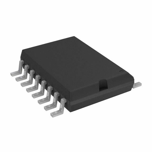
| 描述 | IC DRIVER MOSFET 3A DUAL 8-SOIC门驱动器 3A Dual High Speed MOSFET Driver (Lead Free) |
| 产品分类 | PMIC - MOSFET,电桥驱动器 - 外部开关集成电路 - IC |
| 品牌 | Micrel |
| 产品手册 | |
| 产品图片 |
|
| rohs | 符合RoHS无铅 / 符合限制有害物质指令(RoHS)规范要求 |
| 产品系列 | 电源管理 IC,门驱动器,Micrel MIC4425YM- |
| 数据手册 | |
| 产品型号 | MIC4425YM |
| 上升时间 | 35 ns |
| 下降时间 | 35 ns |
| 产品 | MOSFET Gate Drivers |
| 产品目录页面 | |
| 产品种类 | 门驱动器 |
| 供应商器件封装 | 8-SOIC |
| 其它名称 | 576-1796-5 |
| 包装 | 管件 |
| 商标 | Micrel |
| 安装类型 | 表面贴装 |
| 安装风格 | SMD/SMT |
| 封装 | Tube |
| 封装/外壳 | 8-SOIC(0.154",3.90mm 宽) |
| 封装/箱体 | SOIC-8 |
| 工作温度 | -40°C ~ 85°C |
| 工厂包装数量 | 95 |
| 延迟时间 | 33ns |
| 最大工作温度 | + 85 C |
| 最小工作温度 | - 40 C |
| 标准包装 | 95 |
| 激励器数量 | 2 |
| 电压-电源 | 4.5 V ~ 18 V |
| 电流-峰值 | 3A |
| 电源电压-最大 | 18 V |
| 电源电压-最小 | 4.5 V |
| 电源电流 | 3.5 mA |
| 类型 | Dual Low-Side MOSFET Driver |
| 系列 | MIC4425 |
| 输入类型 | 反相和非反相 |
| 输出数 | 2 |
| 输出电流 | 3 A |
| 输出端数量 | 2 |
| 配置 | Inverting, Non-Inverting |
| 配置数 | 2 |
| 高压侧电压-最大值(自举) | - |


- 商务部:美国ITC正式对集成电路等产品启动337调查
- 曝三星4nm工艺存在良率问题 高通将骁龙8 Gen1或转产台积电
- 太阳诱电将投资9.5亿元在常州建新厂生产MLCC 预计2023年完工
- 英特尔发布欧洲新工厂建设计划 深化IDM 2.0 战略
- 台积电先进制程称霸业界 有大客户加持明年业绩稳了
- 达到5530亿美元!SIA预计今年全球半导体销售额将创下新高
- 英特尔拟将自动驾驶子公司Mobileye上市 估值或超500亿美元
- 三星加码芯片和SET,合并消费电子和移动部门,撤换高东真等 CEO
- 三星电子宣布重大人事变动 还合并消费电子和移动部门
- 海关总署:前11个月进口集成电路产品价值2.52万亿元 增长14.8%


PDF Datasheet 数据手册内容提取
MIC4423/4424/4425 Micrel, Inc. MIC4423/4424/4425 Dual 3A-Peak Low-Side MOSFET Driver Bipolar/CMOS/DMOS Process General Description Features The MIC4423/4424/4425 family are highly reliable BiCMOS/ • Reliable, low-power bipolar/CMOS/DMOS construction DMOS buffer/driver/MOSFET drivers. They are higher out- • Latch-up protected to >500mA reverse current put current versions of the MIC4426/4427/4428, which are • Logic input withstands swing to –5V improved versions of the MIC426/427/428. All three families • High 3A-peak output current are pin-compatible. The MIC4423/4424/4425 drivers are ca- • Wide 4.5V to 18V operating range pable of giving reliable service in more demanding electrical • Drives 1800pF capacitance in 25ns environments than their predecessors. They will not latch • Short <40ns typical delay time under any conditions within their power and voltage ratings. • Delay times consistent with in supply voltage change They can survive up to 5V of noise spiking, of either polarity, • Matched rise and fall times on the ground pin. They can accept, without either damage • TTL logic input independent of supply voltage or logic upset, up to half an amp of reverse current (either • Low equivalent 6pF input capacitance polarity) forced back into their outputs. • Low supply current 3.5mA with logic-1 input The MIC4423/4424/4425 series drivers are easier to use, more 350µA with logic-0 input flexible in operation, and more forgiving than other CMOS • Low 3.5Ω typical output impedance or bipolar drivers currently available. Their BiCMOS/DMOS • Output voltage swings within 25mV of ground or V . construction dissipates minimum power and provides rail-to- S • ‘426/7/8-, ‘1426/7/8-, ‘4426/7/8-compatible pinout rail voltage swings. • Inverting, noninverting, and differential configurations Primarily intended for driving power MOSFETs, the MIC4423/4424/4425 drivers are suitable for driving other loads (capacitive, resistive, or inductive) which require low-imped- ance, high peak currents, and fast switching times. Heavily loaded clock lines, coaxial cables, or piezoelectric transducers are some examples. The only known limitation on loading is that total power dissipated in the driver must be kept within the maximum power dissipation limits of the package. Note: See MIC4123/4124/4125 for high power and narrow pulse applications. Functional Diagram V S Integrated Component Count: 4 Resistors 0.6mA INVERTING 4 Capacitors 0.1mA 52 Transistors OUTA INA 2kΩ NONINVERTING 0.6mA INVERTING 0.1mA OUTB INB 2kΩ NONINVERTING GND Ground Unused Inputs Micrel, Inc. • 2180 Fortune Drive • San Jose, CA 95131 • USA • tel + 1 (408) 944-0800 • fax + 1 (408) 474-1000 • http://www.micrel.com July 2005 1 MIC4423/4424/4425
MIC4423/4424/4425 Micrel, Inc. Ordering Information Part Number Temperatre Range Package Configuration Standard Pb-Free MIC4423CWM MIC4423ZWM 0°C to +70°C 16-pin Wide SOIC Dual Inverting MIC4423BWM MIC4423YWM –40°C to +85°C 16-pin Wide SOIC Dual Inverting MIC4423BM MIC4423YM –40°C to +85°C 8-pin SOIC Dual Inverting MIC4423CN MIC4423ZN 0°C to +70°C 8-pin Plastic DIP Dual Inverting MIC4423BN MIC4423YN –40°C to +85°C 8-pin Plastic DIP Dual Inverting MIC4424CWM MIC4424ZWM 0°C to +70°C 16-pin Wide SOIC Dual Non-Inverting MIC4424BWM MIC4424YWM –40°C to +85°C 16-pin Wide SOIC Dual Non-Inverting MIC4424BM MIC4424YM –40°C to +85°C 8-pin SOIC Dual Non-Inverting MIC4424CN MIC4424ZN 0°C to +70°C 8-pin Plastic DIP Dual Non-Inverting MIC4424BN MIC4424YN –40°C to +85°C 8-pin Plastic DIP Dual Non-Inverting MIC4425CWM MIC4425ZWM 0°C to +70°C 16-pin Wide SOIC Inverting + Non-Inverting MIC4425BWM MIC4425YWM –40°C to +85°C 16-pin Wide SOIC Inverting + Non-Inverting MIC4425BM MIC4425YM –40°C to +85°C 8-pin SOIC Inverting + Non-Inverting MIC4425CN Contact Factory 0°C to +70°C 8-pin Plastic DIP Inverting + Non-Inverting MIC4425BN MIC4425YN –40°C to +85°C 8-pin Plastic DIP Inverting + Non-Inverting Pin Configuration Driver Configuration MIC4423xN/M MIC4423xWM NC 1 8 NC 14 OUTA INA 2 7 OUTA INA2 A 7 OUTA INA2 A 15 OUTA WM Package Note: GND 3 6 VS Duplicate GND, VS, OUTA, 10 OUTB INB 4 5 OUTB and OUTB pins must be INB4 B 5 OUTB INB7 B externally connected together. 11 OUTB 8-pin DIP (N) 8-pin SOIC (M) MIC4424xN/M MIC4423xWM 14 OUTA INA2 A 7 OUTA INA2 A NC 1 16 NC 15 OUTA INA 2 15 OUTA 10 OUTB INB4 B 5 OUTB INB7 B NC 3 14 OUTA 11 OUTB GND 4 13 VS GND 5 12 VS MIC4425xN/M MIC4423xWM NC 6 11 OUTB 14 OUTA INA2 A 7 OUTA INA2 A INB 7 10 OUTB 15 OUTA NC 8 9 NC 10 OUTB INB4 B 5 OUTB INB7 B 11 OUTB 16-pin Wide SOIC (WM) Pin Description Pin Number Pin Number Pin Name Pin Function DIP, SOIC Wide SOIC 2 / 4 2 / 7 INA/B Control Input 3 4, 5 GND Ground: Duplicate pins must be externally connected together. 6 12, 13 V Supply Input: Duplicate pins must be externally connected together. S 7 / 5 14, 15 / 10, 11 OUTA/B Output: Duplicate pins must be externally connected together. 1, 8 1, 3, 6, 8, 9, 16 NC not connected MIC4423/4424/4425 2 July 2005
MIC4423/4424/4425 Micrel, Inc. Absolute Maximum Ratings (Note 1) Operating Ratings (Note 2) Supply Voltage ...........................................................+22V Supply Voltage (V ) ......................................+4.5V to +18V S Input Voltage ..................................V + 0.3V to GND – 5V Temperature Range S Junction Temperature ................................................150°C C Version ....................................................0°C to +70°C B Version ................................................–40°C to +85°C Storage Temperature Range ......................–65°C to 150°C Package Thermal Resistance Lead Temperature (10 sec.) ......................................300°C DIP θ .............................................................130°C/W ESD Susceptability, Note 3 .....................................1000V JA DIP θ ...............................................................42°C/W JC Wide-SOIC θ .................................................120°C/W JA Wide-SOIC θ ...................................................75°C/W JC SOIC θ ...........................................................120°C/W JA SOIC θ ............................................................75°C/W JC MIC4423/4424/4425 Electrical Characteristics (Note 5) 4.5V ≤ V ≤ 18V; T = 25°C, bold values indicate –40°C ≤ T ≤ +85°C; unless noted. S A A Symbol Parameter Conditions Min Typ Max Units Input V Logic 1 Input Voltage 2.4 V IH V Logic 0 Input Voltage 0.8 V IL I Input Current 0V ≤ V ≤ V –1 1 µA IN IN S –10 10 µA Output V High Output Voltage V–0.025 V OH S V Low Output Voltage 0.025 V OL R Output Resistance HI State I = 10mA, V = 18V 2.8 5 Ω O OUT S V = 0.8V, I = 10mA, V = 18V 3.7 8 Ω IN OUT S Output Resistance LO State I = 10mA, V = 18V 3.5 5 Ω OUT S V = 2.4V, I = 10mA, V = 18V 4.3 8 Ω IN OUT S I Peak Output Current 3 A PK I Latch-Up Protection >500 mA Withstand Reverse Current Switching Time (Note 4) t Rise Time test Figure 1, C = 1800pF 23 35 ns R L 28 60 ns t Fall Time test Figure 1, C = 1800pF 25 35 ns F L 32 60 ns t Delay Tlme test Ffigure 1, C = 1800pF 33 75 ns D1 L 32 100 ns t Delay Time test Figure 1, C = 1800pF 38 75 ns D2 L 38 100 ns t Pulse Width test Figure 1 400 ns PW Power Supply I Power Supply Current V = 3.0V (both inputs) 1.5 2.5 mA S IN 2 3.5 mA I Power Supply Current V = 0.0V (both inputs) 0.15 0.25 mA S IN 0.2 0.3 mA Note 1. Exceeding the absolute maximum rating may damage the device. Note 2. The device is not guaranteed to function outside its operating rating. Note 3. Devices are ESD sensitive. Handling precautions recommended. ESD tested to human body model, 1.5k in series with 100pF. Note 4. Switching times guaranteed by design. Note 5. Specification for packaged product only. July 2005 3 MIC4423/4424/4425
MIC4423/4424/4425 Micrel, Inc. Test Circuit V = 18V V = 18V S S 0.1µF 4.7µF 0.1µF 4.7µF INA A OUTA INA A OUTA 1800pF 1800pF MIC4423 MIC4424 INB B OUTB INB B OUTB 1800pF 1800pF 5V 5V 2.5V 2.5V 90% 90% INPUT t ≥ 0.5µs INPUT t ≥ 0.5µs 10% PW 10% PW 0V 0V t t PW PW t t t t t t t t D1 F D2 R D1 R D2 F V V S S 90% 90% OUTPUT OUTPUT 10% 10% 0V 0V Figure 1a. Inverting Driver Switching Time Figure 1b. Noninverting Driver Switching Time MIC4423/4424/4425 4 July 2005
MIC4423/4424/4425 Micrel, Inc. Typical Characteristic Curves Rise Time vs. Fall Time vs. Rise Time Supply Voltage Supply Voltage vs. Capacitive Load 100 100 100 4700pF 4700pF 80 80 80 5V 1800pF 1800pF ns) 60 3300pF 1000pF ns)60 3300pF 1000pF ns)60 12V T (RISE40 2200pF T (FALL40 2200pF T (RISE40 20 20 20 18V 470pF 470pF 0 0 0 4 6 8 10 12 14 16 18 4 6 8 10 12 14 16 18 100 1000 10000 V (V) V (V) C (pF) SUPPLY SUPPLY LOAD Fall Time vs. Rise and Fall Time Propagation Delay vs. Capacitive Load vs. Temperature Input Amplitude 100 40 50 V =18V V =18V S S C =1800pF C =1800pF 80 5V LOAD 40 LOAD 30 T F T (ns)FALL4600 12V TIME (ns)20 TR T (ns)2300 TTDD12 10 20 18V 10 0 0 0 100 1000 10000 -75 -30 15 60 105 150 0 2 4 6 8 10 12 C (pF) JUNCTION TEMPERATURE (˚C) INPUT (V) LOAD Supply Current vs. Supply Current Supply Current vs. Capacitive Load vs. Frequency Capacitive Load 100 100 100 V =18V V =18V V =12V 90 SUPPLY 90 SUPPLY 90 SUPPLY 80 80 10000pF 80 2MHz A) 70 A) 70 A) 70 m 60 m 60 m 60 I (SUPPLY345000 20kH5z00kHz I (SUPPLY345000 1001p0F00pF 3300pF I (SUPPLY345000 500kHz 20 100kHz 20 20 20kHz 100kHz 10 10 10 0 0 0 100 1000 10000 10 100 1000 100 1000 10000 C (pF) FREQUENCY (kHz) C (pF) LOAD LOAD Supply Current Supply Current vs. Supply Current vs. Frequency Capacitive Load vs. Frequency 100 100 100 V =12V V =5V V =5V 90 SUPPLY 90 SUPPLY 90 SUPPLY 80 80 80 10000pF 10000pF 70 70 70 mA) 60 mA) 60 mA) 60 4700pF I (SUPPLY345000 10100p0F0pF 3300pF I (SUPPLY345000 100kHz 2MH5z00kHz I (SUPPLY345000 1001p0F002p2F00pF 20 20 20 10 10 10 0 0 0 10 100 1000 100 1000 10000 10 100 1000 FREQUENCY (kHz) C (pF) FREQUENCY (kHz) LOAD July 2005 5 MIC4423/4424/4425
MIC4423/4424/4425 Micrel, Inc. Delay Time vs. Delay Time Quiescent Sypply Current Supply Voltage vs. Temperature vs. Voltage 60 60 10 CLOAD=2200 pF CLOAD=2200pF TJ=25˚C 50 50 40 40 mA) 1 BOTH INPUTS=1 s) TD2 s) TD2 (T n30 n30 N T (20 TD1 T (20 TD1 UIESCE0.1 BOTH INPUTS=0 Q I 10 10 0 0 0.01 4 6 8 10 12 14 16 18 -55 -25 5 35 65 95 125 4 6 8 10 12 14 16 18 V (V) TEMPERATURE (˚C) V (V) SUPPLY SUPPLY Quiescent Current Output Resistance (Output Output Resistance (Output vs. Temperature High) vs. Supply Voltage Low) vs. Supply Voltage 1.4 6 6 V =10V S 1.2 5 5 125˚C (mA)UIESCENT001...680 INPUTS=1 R(Ω)DS(ON)234 12255˚˚CC R(Ω)DS(ON)234 25˚C Q0.4 I 0.2 INPUTS=0 1 1 0 0 0 -55 -25 5 35 65 95 125 4 6 8 10 12 14 16 18 4 6 8 10 12 14 16 18 TEMPERATURE (˚C) V (V) V (V) SUPPLY SUPPLY MIC4423/4424/4425 6 July 2005
MIC4423/4424/4425 Micrel, Inc. Application Information requires attention to the ground path. Two things other than the driver affect the rate at which it is possible to turn a load Although the MIC4423/24/25 drivers have been specifically off: The adequacy of the grounding available for the driver, constructed to operate reliably under any practical circum- and the inductance of the leads from the driver to the load. stances, there are nonetheless details of usage which will The latter will be discussed in a separate section. provide better operation of the device. Best practice for a ground path is obviously a well laid out Supply Bypassing ground plane. However, this is not always practical, and a Charging and discharging large capacitive loads quickly poorly-laid out ground plane can be worse than none. Attention requires large currents. For example, charging 2000pF from to the paths taken by return currents even in a ground plane 0 to 15 volts in 20ns requires a constant current of 1.5A. In is essential. In general, the leads from the driver to its load, practice, the charging current is not constant, and will usually the driver to the power supply, and the driver to whatever is peak at around 3A. In order to charge the capacitor, the driver driving it should all be as low in resistance and inductance must be capable of drawing this much current, this quickly, as possible. Of the three paths, the ground lead from the from the system power supply. In turn, this means that as far driver to the logic driving it is most sensitive to resistance or as the driver is concerned, the system power supply, as seen inductance, and ground current from the load are what is most by the driver, must have a VERY low impedance. likely to cause disruption. Thus, these ground paths should be arranged so that they never share a land, or do so for as As a practical matter, this means that the power supply bus short a distance as is practical. must be capacitively bypassed at the driver with at least 100X the load capacitance in order to achieve optimum To illustrate what can happen, consider the following: The driving speed. It also implies that the bypassing capacitor inductance of a 2cm long land, 1.59mm (0.062") wide on a must have very low internal inductance and resistance at PCB with no ground plane is approximately 45nH. Assum- all frequencies of interest. Generally, this means using two ing a dl/dt of 0.3A/ns (which will allow a current of 3A to flow capacitors, one a high-performance low ESR film, the other after 10ns, and is thus slightly slow for our purposes) a volt- a low internal resistance ceramic, as together the valleys in age of 13.5 Volts will develop along this land in response to their two impedance curves allow adequate performance over our postulated ∆Ι. For a 1cm land, (approximately 15nH) 4.5 a broad enough band to get the job done. PLEASE NOTE Volts is developed. Either way, anyone using TTL-level input that many film capacitors can be sufficiently inductive as to signals to the driver will find that the response of their driver be useless for this service. Likewise, many multilayer ceramic has been seriously degraded by a common ground path for capacitors have unacceptably high internal resistance. Use input to and output from the driver of the given dimensions. capacitors intended for high pulse current service (in-house Note that this is before accounting for any resistive drops in we use WIMA™ film capacitors and AVX Ramguard™ ceram- the circuit. The resistive drop in a 1.59mm (0.062") land of ics; several other manufacturers of equivalent devices also 2oz. Copper carrying 3A will be about 4mV/cm (10mV/in) at exist). The high pulse current demands of capacitive drivers DC, and the resistance will increase with frequency as skin also mean that the bypass capacitors must be mounted effect comes into play. very close to the driver in order to prevent the effects of lead inductance or PCB land inductance from nullifying what you The problem is most obvious in inverting drivers where the are trying to accomplish. For optimum results the sum of the input and output currents are in phase so that any attempt lengths of the leads and the lands from the capacitor body to to raise the driver’s input voltage (in order to turn the driver’s the driver body should total 2.5cm or less. load off) is countered by the voltage developed on the com- mon ground path as the driver attempts to do what it was Bypass capacitance, and its close mounting to the driver serves supposed to. It takes very little common ground path, under two purposes. Not only does it allow optimum performance these circumstances, to alter circuit operation drastically. from the driver, it minimizes the amount of lead length radiat- ing at high frequency during switching, (due to the large Δ I) Output Lead Inductance thus minimizing the amount of EMI later available for system The same descriptions just given for PCB land inductance disruption and subsequent cleanup. It should also be noted apply equally well for the output leads from a driver to its load, that the actual frequency of the EMI produced by a driver is except that commonly the load is located much further away not the clock frequency at which it is driven, but is related to from the driver than the driver’s ground bus. the highest rate of change of current produced during switch- ing, a frequency generally one or two orders of magnitude Generally, the best way to treat the output lead inductance higher, and thus more difficult to filter if you let it permeate your problem, when distances greater than 4cm (2") are involved, system. Good bypassing practice is essential to proper requires treating the output leads as a transmission line. Un- fortunately, as both the output impedance of the driver and the operation of high speed driver ICs. input impedance of the MOSFET gate are at least an order of Grounding magnitude lower than the impedance of common coax, using Both proper bypassing and proper grounding are necessary coax is seldom a cost-effective solution. A twisted pair works for optimum driver operation. Bypassing capacitance only about as well, is generally lower in cost, and allows use of a allows a driver to turn the load ON. Eventually (except in rare wider variety of connectors. The second wire of the twisted circumstances) it is also necessary to turn the load OFF. This pair should carry common from as close as possible to the July 2005 7 MIC4423/4424/4425
MIC4423/4424/4425 Micrel, Inc. ground pin of the driver directly to the ground terminal of the ible with TTL signals, or with CMOS powered from any supply load. Do not use a twisted pair where the second wire in the voltage between 3V and 15V. pair is the output of the other driver, as this will not provide a The MIC4423/24/25 drivers can also be driven directly by the complete current path for either driver. Likewise, do not use SG1524/25/26/27, TL494/95, TL594/95, NE5560/61/62/68, a twisted triad with two outputs and a common return unless TSC170, MIC38C42, and similar switch mode power supply both of the loads to be driver are mounted extremely close ICs. By relocating the main switch drive function into the driver to each other, and you can guarantee that they will never be rather than using the somewhat limited drive capabilities of a switching at the same time. PWM IC. The PWM IC runs cooler, which generally improves For output leads on a printed circuit, the general rule is to make its performance and longevity, and the main switches switch them as short and as wide as possible. The lands should also faster, which reduces switching losses and increase system be treated as transmission lines: i.e. minimize sharp bends, efficiency. or narrowings in the land, as these will cause ringing. For a The input protection circuitry of the MIC4423/24/25, in addi- rough estimate, on a 1.59mm (0.062") thick G-10 PCB a pair tion to providing 2kV or more of ESD protection, also works to of opposing lands each 2.36mm (0.093") wide translates to a prevent latchup or logic upset due to ringing or voltage spiking characteristic impedance of about 50Ω. Half that width suffices on the logic input terminal. In most CMOS devices when the on a 0.787mm (0.031") thick board. For accurate impedance logic input rises above the power supply terminal, or descends matching with a MIC4423/24/25 driver, on a 1.59mm (0.062") below the ground terminal, the device can be destroyed or board a land width of 42.75mm (1.683") would be required, rendered inoperable until the power supply is cycled OFF due to the low impedance of the driver and (usually) its load. and ON. The MIC4423/24/25 drivers have been designed to This is obviously impractical under most circumstances. prevent this. Input voltages excursions as great as 5V below Generally the tradeoff point between lands and wires comes ground will not alter the operation of the device. Input excur- when lands narrower than 3.18mm (0.125") would be required sions above the power supply voltage will result in the excess on a 1.59mm (0.062") board. voltage being conducted to the power supply terminal of the To obtain minimum delay between the driver and the load, it IC. Because the excess voltage is simply conducted to the is considered best to locate the driver as close as possible to power terminal, if the input to the driver is left in a high state the load (using adequate bypassing). Using matching trans- when the power supply to the driver is turned off, currents as formers at both ends of a piece of coax, or several matched high as 30mA can be conducted through the driver from the lengths of coax between the driver and the load, works in input terminal to its power supply terminal. This may overload theory, but is not optimum. the output of whatever is driving the driver, and may cause other devices that share the driver’s power supply, as well as Driving at Controlled Rates the driver, to operate when they are assumed to be off, but Occasionally there are situations where a controlled rise or it will not harm the driver itself. Excessive input voltage will fall time (which may be considerably longer than the normal also slow the driver down, and result in much longer internal rise or fall time of the driver’s output) is desired for a load. In propagation delays within the drivers. T , for example, may D2 such cases it is still prudent to employ best possible practice increase to several hundred nanoseconds. In general, while in terms of bypassing, grounding and PCB layout, and then the driver will accept this sort of misuse without damage, reduce the switching speed of the load (NOT the driver) by proper termination of the line feeding the driver so that line adding a noninductive series resistor of appropriate value spiking and ringing are minimized, will always result in faster between the output of the driver and the load. For situations and more reliable operation of the device, leave less EMI to where only rise or only fall should be slowed, the resistor can be filtered elsewhere, be less stressful to other components be paralleled with a fast diode so that switching in the other in the circuit, and leave less chance of unintended modes of direction remains fast. Due to the Schmitt-trigger action of the operation. driver’s input it is not possible to slow the rate of rise (or fall) of the driver’s input signal to achieve slowing of the output. Power Dissipation CMOS circuits usually permit the user to ignore power dis- Input Stage sipation. Logic families such as 4000 series and 74Cxxx have The input stage of the MIC4423/24/25 consists of a single- outputs which can only source or sink a few milliamps of cur- MOSFET class A stage with an input capacitance of ≤38pF. rent, and even shorting the output of the device to ground or This capacitance represents the maximum load from the V may not damage the device. CMOS drivers, on the other CC driver that will be seen by its controlling logic. The drain load hand, are intended to source or sink several Amps of current. on the input MOSFET is a –2mA current source. Thus, the This is necessary in order to drive large capacitive loads at quiescent current drawn by the driver varies, depending on frequencies into the megahertz range. Package power dis- the logic state of the input. sipation of driver ICs can easily be exceeded when driving large loads at high frequencies. Care must therefore be paid Following the input stage is a buffer stage which provides to device dissipation when operating in this domain. ~400mV of hysteresis for the input, to prevent oscillations when slowly-changing input signals are used or when noise The Supply Current vs Frequency and Supply Current vs is present on the input. Input voltage switching threshold is Load characteristic curves furnished with this data sheet approximately 1.5V which makes the driver directly compat- aid in estimating power dissipation in the driver. Operating MIC4423/4424/4425 8 July 2005
MIC4423/4424/4425 Micrel, Inc. frequency, power supply voltage, and load all affect power However, in this instance the R required may be either the on O dissipation. resistance of the driver when its output is in the high state, or its on resistance when the driver is in the low state, depending Given the power dissipation in the device, and the thermal on how the inductor is connected, and this is still only half the resistance of the package, junction operating temperature story. For the part of the cycle when the inductor is forcing for any ambient is easy to calculate. For example, the ther- current through the driver, dissipation is best described as mal resistance of the 8-pin plastic DIP package, from the datasheet, is 150°C/W. In a 25°C ambient, then, using a P = I V (1 – D) L2 D maximum junction temperature of 150°C, this package will where V is the forward drop of the clamp diode in the driver dissipate 960mW. D (generally around 0.7V). The two parts of the load dissipation Accurate power dissipation numbers can be obtained by sum- must be summed in to produce P L ming the three sources of power dissipation in the device: P = P + P L L1 L2 • Load power dissipation (P ) L Quiescent Power Dissipation • Quiescent power dissipation (P ) Q • Transition power dissipation (P ) Quiescent power dissipation (P , as described in the input T Q section) depends on whether the input is high or low. A low Calculation of load power dissipation differs depending on input will result in a maximum current drain (per driver) of whether the load is capacitive, resistive or inductive. ≤0.2mA; a logic high will result in a current drain of ≤2.0mA. Quiescent power can therefore be found from: Resistive Load Power Dissipation Dissipation caused by a resistive load can be calculated as: P = V [D I + (1 – D) I ] Q S H L P = I2 R D where: L O where: I = quiescent current with input high H I = quiescent current with input low I = the current drawn by the load L D = fraction of time input is high (duty cycle) R = the output resistance of the driver when the O V = power supply voltage output is high, at the power supply voltage used S (See characteristic curves) Transition Power Dissipation D = fraction of time the load is conducting (duty cycle) Transition power is dissipated in the driver each time its output changes state, because during the transition, for a Capacitive Load Power Dissipation very brief interval, both the N- and P-channel MOSFETs in Dissipation caused by a capacitive load is simply the energy the output totem-pole are ON simultaneously, and a current placed in, or removed from, the load capacitance by the is conducted through them from V to ground. The transition driver. The energy stored in a capacitor is described by the S power dissipation is approximately: equation: P = f V (A•s) E = 1/2 C V2 T S where (A•s) is a time-current factor derived from Figure 2. As this energy is lost in the driver each time the load is charged or discharged, for power dissipation calculations the 1/2 is Total power (PD) then, as previously described is just removed. This equation also shows that it is good practice P = P + P +P not to place more voltage in the capacitor than is necessary, D L Q T as dissipation increases as the square of the voltage applied Examples show the relative magnitude for each term. to the capacitor. For a driver with a capacitive load: EXAMPLE 1: A MIC4423 operating on a 12V supply driving P = f C (V )2 two capacitive loads of 3000pF each, operating at 250kHz, L S with a duty cycle of 50%, in a maximum ambient of 60°C. where: First calculate load power loss: f = Operating Frequency C = Load Capacitance P = f x C x (V )2 L S V = Driver Supply Voltage P = 250,000 x (3 x 10–9 + 3 x 10–9) x 122 S L = 0.2160W Inductive Load Power Dissipation For inductive loads the situation is more complicated. For Then transition power loss: the part of the cycle in which the driver is actively forcing P = f x V x (A•s) current into the inductor, the situation is the same as it is in T S = 250,000 • 12 • 2.2 x 10–9 = 6.6mW the resistive case: P = I2 R D L1 O July 2005 9 MIC4423/4424/4425
MIC4423/4424/4425 Micrel, Inc. Then quiescent power loss: then: P = V x [D x I + (1 – D) x I ] P = 0.174 + 0.025 + 0.0150 Q S H L D = 12 x [(0.5 x 0.0035) + (0.5 x 0.0003)] = 0.213W = 0.0228W In a ceramic package with an θ of 100°C/W, this amount of JA Total power dissipation, then, is: power results in a junction temperature given the maximum 40°C ambient of: P = 0.2160 + 0.0066 + 0.0228 D = 0.2454W (0.213 x 100) + 40 = 61.4°C Assuming an SOIC package, with an θ of 120°C/W, this will The actual junction temperature will be lower than calculated JA result in the junction running at: both because duty cycle is less than 100% and because the graph lists R at a T of 125°C and the R at 61°C T 0.2454 x 120 = 29.4°C DS(on) J DS(on) J will be somewhat lower. above ambient, which, given a maximum ambient tempera- Definitions ture of 60°C, will result in a maximum junction temperature C = Load Capacitance in Farads. of 89.4°C. L D = Duty Cycle expressed as the fraction of time the input EXAMPLE 2: A MIC4424 operating on a 15V input, with one to the driver is high. driver driving a 50Ω resistive load at 1MHz, with a duty cycle of 67%, and the other driver quiescent, in a maximum ambi- f = Operating Frequency of the driver in Hertz ent temperature of 40°C: I = Power supply current drawn by a driver when both P = I2 x R x D H inputs are high and neither output is loaded. L O First, I must be determined. I = Power supply current drawn by a driver when both O L inputs are low and neither output is loaded. I = V / (R + R ) O S O LOAD I = Output current from a driver in Amps. Given R from the characteristic curves then, D O P = Total power dissipated in a driver in Watts. I = 15 / (3.3 + 50) D O P = Power dissipated in the driver due to the driver’s I = 0.281A L O load in Watts. and: P = Power dissipated in a quiescent driver in Watts. Q P = (0.281)2 x 3.3 x 0.67 P = Power dissipated in a driver when the output L T = 0.174W changes states (“shoot-through current”) in Watts. P = F x V x (A•s)/2 NOTE: The “shoot-through” current from a dual T S transition (once up, once down) for both drivers is (because only one side is operating) stated in the graph on the following page in ampere- = (1,000,000 x 15 x 3.3 x 10–9) / 2 nanoseconds. This figure must be multiplied by the = 0.025 W number of repetitions per second (frequency to find Watts). and: R = Output resistance of a driver in Ohms. P = 15 x [(0.67 x 0.00125) + (0.33 x 0.000125) + O Q (1 x 0.000125)] V = Power supply voltage to the IC in Volts. S (this assumes that the unused side of the driver has its input grounded, which is more efficient) = 0.015W MIC4423/4424/4425 10 July 2005
MIC4423/4424/4425 Micrel, Inc. Crossover Energy Loss 10-8 ) s d n o c e s - e10-9 r e p m A ( s • A 10-10 0 2 4 6 8 10 12 14 16 18 V IN NOTE: THE VALUES ON THIS GRAPH REPRESENT THE LOSS SEEN BY BOTH DRIVERS IN A PACKAGE DURING ONE COMPLETE CYCLE. FOR A SINGLE DRIVER DIVIDE THE STATED VALUES BY 2. FOR A SINGLE TRANSITION OF A SINGLE DRIVER, DIVIDE THE STATED VALUE BY 4. Figure 2. 1250 W) AGEN (m1000 SOIC KO ACATI 750 PP M SI MUDIS 500 PDIP XIR AE MW 250 O P 0 25 50 75 100 125 150 AMBIENT TEMPERATURE (°C) July 2005 11 MIC4423/4424/4425
MIC4423/4424/4425 Micrel, Inc. Package Information PIN 1 DIMENSIONS: INCH (MM) 0.380 (9.65) 0.255 (6.48) 0.370 (9.40) 0.135 (3.43) 0.245 (6.22) 0.125 (3.18) 0.300 (7.62) 0.013 (0.330) 0.010 (0.254) 0.018 (0.57) 0.130 (3.30) 0.380 (9.65) 0.320 (8.13) 0.100 (2.54) 0.0375 (0.952) 8-Pin Plastic DIP (N) 8-Pin SOIC (M) MIC4423/4424/4425 12 July 2005
MIC4423/4424/4425 Micrel, Inc. PIN 1 DIMENSIONS: INCHES (MM) 0.301 (7.645) 0.297 (7.544) 0.027 (0.686) 0.031 (0.787) 0.103 (2.616) 0.297 (7.544) 0.050 (1.270) 0.016 (0.046) 0.099 (2.515) 0.293 (7.442) TYP TYP 7 0.022 (0.559) TYP 0.018 (0.457) 0.015 R (0.381) 5 0.409 (10.389) 0.015 0.330 (8.382) TYP 0.094 (2.388) 0.405 (10.287) (0.381) 0.326 (8.280) 10 TYP 0.090 (2.286) SEATING MIN 0.032 (0.813) TYP PLANE 0.408 (10.363) 0.404 (10.262) 16-Pin Wide SOIC (WM) MICREL INC. 2180 FORTUNE DRIVE SAN JOSE, CA 95131 USA TEL + 1 (408) 944-0800 FAX + 1 (408) 474-1000 WEB http://www.micrel.com This information furnished by Micrel in this data sheet is believed to be accurate and reliable. However no responsibility is assumed by Micrel for its use. Micrel reserves the right to change circuitry and specifications at any time without notification to the customer. Micrel Products are not designed or authorized for use as components in life support appliances, devices or systems where malfunction of a product can reasonably be expected to result in personal injury. Life support devices or systems are devices or systems that (a) are intended for surgical implant into the body or (b) support or sustain life, and whose failure to perform can be reasonably expected to result in a significant injury to the user. A Purchaser’s use or sale of Micrel Products for use in life support appliances, devices or systems is a Purchaser’s own risk and Purchaser agrees to fully indemnify Micrel for any damages resulting from such use or sale. © 1999 Micrel, Inc. July 2005 13 MIC4423/4424/4425
Mouser Electronics Authorized Distributor Click to View Pricing, Inventory, Delivery & Lifecycle Information: M icrel: MIC4423YM TR MIC4425YWM TR MIC4424YWM TR M icrochip: MIC4424YN MIC4425YWM MIC4425YN MIC4425BWM MIC4425CWM MIC4424ZN MIC4423CWM MIC4424YM MIC4424ZWM MIC4424YWM MIC4423YN MIC4423YM MIC4425ZWM MIC4423YWM MIC4424BWM MIC4423ZWM MIC4423ZN MIC4425YM MIC4423BWM MIC4424CWM-TR MIC4424BWM-TR MIC4425CWM-TR MIC4423BWM-TR MIC4425BWM-TR MIC4423CWM-TR MIC4425YM-TR MIC4425ZWM-TR MIC4424ZWM-TR MIC4423ZWM-TR MIC4424YM-TR MIC4424YWM-TR MIC4423YM-TR MIC4425YWM-TR MIC4423YWM-TR