ICGOO在线商城 > 集成电路(IC) > PMIC - 配电开关,负载驱动器 > MCZ33996EKR2
 Datasheet下载
- 型号: MCZ33996EKR2
- 制造商: Freescale Semiconductor
- 库位|库存: xxxx|xxxx
- 要求:
| 数量阶梯 | 香港交货 | 国内含税 |
| +xxxx | $xxxx | ¥xxxx |
查看当月历史价格
查看今年历史价格
MCZ33996EKR2产品简介:
ICGOO电子元器件商城为您提供MCZ33996EKR2由Freescale Semiconductor设计生产,在icgoo商城现货销售,并且可以通过原厂、代理商等渠道进行代购。 MCZ33996EKR2价格参考。Freescale SemiconductorMCZ33996EKR2封装/规格:PMIC - 配电开关,负载驱动器, 。您可以下载MCZ33996EKR2参考资料、Datasheet数据手册功能说明书,资料中有MCZ33996EKR2 详细功能的应用电路图电压和使用方法及教程。
NXP USA Inc.生产的MCZ33996EKR2是一款PMIC(电源管理集成电路),属于配电开关和负载驱动器类别。该型号的应用场景主要包括以下几个方面:

1. 汽车电子系统:
   MCZ33996EKR2广泛应用于汽车电子领域,例如车身控制模块(BCM)、信息娱乐系统、高级驾驶辅助系统(ADAS)等。它能够为多个负载提供高效、可靠的电源管理,支持动态负载切换,满足汽车环境中对稳定性和可靠性的严格要求。

2. 工业自动化:
   在工业设备中,该芯片可用于电机控制、传感器接口和分布式控制系统。其高效的负载驱动能力可以确保工业设备在高功率需求下的稳定运行,同时支持多通道负载分配,简化复杂系统的电源设计。

3. 通信基础设施:
   适用于基站、路由器和其他通信设备中的电源管理。MCZ33996EKR2的高效率和低功耗特性使其成为这些高性能设备的理想选择,能够优化能源使用并减少散热问题。

4. 消费类电子产品:
   在需要多负载管理的消费类设备中,如智能家居控制器、便携式医疗设备或高端音频设备,这款PMIC可以通过精确的电流控制和快速响应时间提升整体性能。

5. 物联网(IoT)设备:
   对于低功耗、高集成度的IoT应用,MCZ33996EKR2可以帮助实现高效的电源分配和管理,延长电池寿命,并支持多种传感器和执行器的协同工作。

总结来说,MCZ33996EKR2凭借其出色的负载驱动能力和灵活的配电功能,在汽车、工业、通信、消费电子及IoT等领域都有广泛的应用前景,尤其适合需要多通道电源管理和高可靠性的工作环境。
| 参数 | 数值 |
| 产品目录 | 集成电路 (IC)半导体 |
| 描述 | IC SWITCH LOSIDE 16-OUTPT 32SOIC电源开关 IC - 配电 16 LOW SIDE SW 1.20HM |
| 产品分类 | PMIC - 电源分配开关集成电路 - IC |
| 品牌 | Freescale Semiconductor |
| 产品手册 | |
| 产品图片 |
|
| rohs | 符合RoHS无铅 / 符合限制有害物质指令(RoHS)规范要求 |
| 产品系列 | 开关 IC,电源开关 IC - 配电,Freescale Semiconductor MCZ33996EKR2- |
| 数据手册 | |
| 产品型号 | MCZ33996EKR2 |
| Rds(On) | 550 毫欧 |
| 产品 | Power Switches |
| 产品种类 | 电源开关 IC - 配电 |
| 供应商器件封装 | 32-SOICW 裸露焊盘 |
| 内部开关 | 是 |
| 包装 | 带卷 (TR) |
| 单位重量 | 501 mg |
| 商标 | Freescale Semiconductor |
| 安装类型 | 表面贴装 |
| 安装风格 | SMD/SMT |
| 导通电阻—最大值 | 0.55 Ohms |
| 封装 | Reel |
| 封装/外壳 | 32-SSOP(0.295",7.50mm 宽)裸焊盘 |
| 封装/箱体 | SOIC EP-32 |
| 工作温度 | -40°C ~ 125°C |
| 工厂包装数量 | 1000 |
| 最大工作温度 | + 125 C |
| 最小工作温度 | - 40 C |
| 标准包装 | 1,000 |
| 电压-输入 | 5 V ~ 27 V |
| 电流限制 | 1.2A |
| 电源电流—最大值 | 4 mA |
| 类型 | 低压侧开关 |
| 系列 | MC33996 |
| 输出数 | 16 |
| 输出电流 | 0.9 A |
| 输出端数量 | 16 Output |


- 商务部:美国ITC正式对集成电路等产品启动337调查
- 曝三星4nm工艺存在良率问题 高通将骁龙8 Gen1或转产台积电
- 太阳诱电将投资9.5亿元在常州建新厂生产MLCC 预计2023年完工
- 英特尔发布欧洲新工厂建设计划 深化IDM 2.0 战略
- 台积电先进制程称霸业界 有大客户加持明年业绩稳了
- 达到5530亿美元!SIA预计今年全球半导体销售额将创下新高
- 英特尔拟将自动驾驶子公司Mobileye上市 估值或超500亿美元
- 三星加码芯片和SET,合并消费电子和移动部门,撤换高东真等 CEO
- 三星电子宣布重大人事变动 还合并消费电子和移动部门
- 海关总署:前11个月进口集成电路产品价值2.52万亿元 增长14.8%
_renders/CS4265-CNZR.jpg)


PDF Datasheet 数据手册内容提取
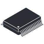
Freescale Semiconductor Document Number: MC33996 Advance Information Rev. 8.0, 8/2008 16 Output Switch with SPI Control 33996 The 33996 is a 16-output low side switch with a 24-bit serial input control. It is designed for a variety of applications including inductive, incandescent, and LED loads. The Serial Peripheral Interface (SPI) LOW SIDE SWITCH provides both input control and diagnostic readout. A Pulse Width Modulation (PWM) control input is provided for pulse width modulation of multiple outputs at the same duty cycle. A dedicated reset input provides the ability to clear all internal registers and turn all outputs off. The 33996 directly interfaces with micro controllers and is compatible with both 3.3 and 5.0V CMOS logic levels. The 33996, in effect, serves as a bus expander and buffer with fault management features that reduce the MCU’s fault management burden. Features • Designed to operate 5.0V < V < 27V PWR • 24 Bit SPI for control and fault reporting, 3.3/5.0V compatible EK SUFFIX (PB-FREE) • Outputs are current limited (0.9 to 2.5A) to drive incandescent 98ARL10543D 32-PIN SOICW EXPOSED PAD lamps • Output voltage clamp of +50V during inductive switching • On/Off control of open load detect current (LED application) • VPWR standby current < 10μA ORDERING INFORMATION • R of 0.55Ω at 25°C typical DS(ON) Temperature • Independent over-temperature protection Device Package Range (T ) A • Output selectable for PWM control MC33996EK/R2 • Output ON short-to-V and off short-to-ground /open detection BAT -40°C to 125°C 32 SOICW-EP • Pb-free packaging designated by suffix code EK MCZ33996EK/R2 Vdd 3.3 V/5.0 V VPWR VBAT 33996 VDD SOPWR VPWR MCU SCLK SCLK OUT0 CS CS OUT1 Solenoid/Relay MISO SI OUT2 OUT3 MOSI SO OUT4 PWM PWM OUT5 RST RST OUT6 OUT7 OUT8 LED OUT9 OUT10 OUT11 OUT12 OUT13 OUT14 OUT15 /8 Lamp GND Figure 1. 33996 Simplified Application Diagram * This document contains certain information on a new product. Specifications and information herein are subject to change without notice. © Freescale Semiconductor, Inc., 2007-2008. All rights reserved.
IINTERNAL BLOCK DIAGRAM IINTERNAL BLOCK DIAGRAM VPWR OUT0 VDD Over-voltage Voltage VDD Detect Regulator Bias 50V OVD GE PWM V OT Gate 10μA RBDD OSFF Control To Gates RST 25μA SFPDB 1 to 15 OUT1-15 SFL CS 10μA CS VRef SCLK Open Input SI Load ILimit Buffers Detect SCLK SCOSI Enable 50μA RS 10μA CSBI SI Short and 10 μA SPI Open GND (8) Load Interface Detect SO Serial D/O Logic Line Driver Over-temperature Detect SOPWR From Detectors 1 to 15 Figure 2. 33996 Simplified Internal Block Diagram 33996 Analog Integrated Circuit Device Data 2 Freescale Semiconductor
PIN CONNECTIONS PIN CONNECTIONS OUT0 1 32 OUT15 OUT1 2 31 OUT14 SOPWR 3 30 PWM OUT2 4 29 OUT13 OUT3 5 28 OUT12 VPWR 6 27 RST GND 7 26 GND GND 8 25 GND GND 9 24 GND GND 10 23 GND SCLK 11 22 SO OUT4 12 21 OUT11 OUT5 13 20 OUT10 CS 14 19 SI OUT6 15 18 OUT9 OUT7 16 17 OUT8 Figure 3. 33996 Pin Locations Table 1. Pin Definitions A functional description of each pin can be found in the Functional Pin Description section beginning on page 10. Pin Pin Name Formal Name Definition 1, 2, 4, 5, 12, 13, OUT0 – OUT15 Output 0 – Output 15 Open drain output pin. 15 – 18, 20, 21, 28, 29, 31, 32 3 SOPWR SO Supply Power supply pin to the SO output driver. PWR 6 VPWR Battery Input Battery supply input pin. 7– 10, 23 – 26 GND Ground Ground for logic, analog, and power output devices. 11 SCLK System Clock System Clock for internal shift registers of the 33996. 14 CS Chip Select SPI control chip select input pin from the MCU to the 33996. 19 SI Serial Input Serial data input pin to the 33996. 22 SO Serial Output Serial data output pin. 27 RST Reset Active low reset input pin. 30 PWM PWM Control PWM control input pin. Supports PWM on any combination of outputs. 33 EP Exposed Pad Device will perform as specified with the Exposed Pad un-terminated (floating) however, it is recommended that the Exposed Pad be terminated to system ground. 33996 Analog Integrated Circuit Device Data Freescale Semiconductor 3
ELECTRICAL CHARACTERISTICS MAXIMUM RATINGS ELECTRICAL CHARACTERISTICS MAXIMUM RATINGS Table 2. Maximum Ratings All voltages are with respect to ground unless otherwise noted. Rating Symbol Value Unit ELECTRICAL RATINGS VPWR Supply Voltage (1) V -1.5 to 50 V PWR SO Output Driver Power Supply Voltage (1) SO -0.3 to 7.0 V PWR SPI Interface Logic Input Voltage (CS, PWM, SI, SO, SCLK, RST) (1) V -0.3 to 7.0 V IN Output Drain Voltage V -0.3 to 45 V D Frequency of SPI Operation (2) f 6.0 MHz SPI Output Clamp Energy (3) E 50 mJ CLAMP ESD Voltage (4) V Human Body Model V ±2000 ESD1 Machine Model V ±200 ESD2 THERMAL RATINGS Operating Temperature °C Ambient T -40 to 125 A Junction T -40 to 150 J Case T -40 to 125 C Storage Temperature T -55 to 150 °C STG Power Dissipation (TA = 25°C) (5) PD 1.7 W Peak Package Reflow Temperature During Reflow (6), (7) T Note 7 °C PPRT Thermal Resistance °C/W Junction-to-Ambient (8) RθJA 75 Junction- to-Lead (9) RθJL 8.0 Junction-to-Flag RθJC 1.2 Notes 1. Exceeding these limits may cause malfunction or permanent damage to the device. 2. This parameter is guaranteed by design but not production tested. 3. Maximum output clamp energy capability at 150°C junction temperature using single nonrepetitive pulse method. 4. ESD data available upon request. ESD testing is performed in accordance with the Human Body Model (C = 100pF, R = 1500Ω) ZAP ZAP and the Machine Model (C = 200pF, R = 0Ω). ZAP ZAP 5. Maximum power dissipation with no heat sink used. 6. Pin soldering temperature limit is for 10 seconds maximum duration. Not designed for immersion soldering. Exceeding these limits may cause malfunction or permanent damage to the device. 7. Freescale’s Package Reflow capability meets Pb-free requirements for JEDEC standard J-STD-020C. For Peak Package Reflow Temperature and Moisture Sensitivity Levels (MSL), Go to www.freescale.com, search by part number [e.g. remove prefixes/suffixes and enter the core ID to view all orderable parts. (i.e. MC33xxxD enter 33xxx), and review parametrics. 8. Tested per JEDEC test JESD52-2 (single-layer PWB). 9. Tested per JEDEC test JESD51-8 (two-layer PWB). 33996 Analog Integrated Circuit Device Data 4 Freescale Semiconductor
ELECTRICAL CHARACTERISTICS STATIC ELECTRICAL CHARACTERISTICS STATIC ELECTRICAL CHARACTERISTICS Table 3. STATIC ELECTRICAL CHARACTERISTICS Characteristics noted under conditions 3.1V ≤ SO ≤ 5.5V, 5.0V ≤ V ≤ 18V, -40°C ≤ T ≤ 125°C unless otherwise noted. PWR PWR A Where applicable, typical values noted reflect the parameter ‘s approximate value with V = 13V, T = 25°C. PWR A Characteristic Symbol Min Typ Max Unit POWER SUPPLY (VPWR) Supply Voltage Range V V PWR (FO) Fully Operational 5.0 – 27 Supply Current I mA PWR (ON) All Outputs ON, IOUT = 0.3A – 4.0 8.0 Sleep State Supply Current at RST ≤ 0.8 and/or I _ 1.0 10 μA SO ≤ 1.5V PWR (SS) PWR Over-voltage Shutdown V 27.5 31.5 35 V OV Over-voltage Shutdown Hysteresis V 0.6 1.4 2.3 V OV (HYS) VPWR Under-voltage Shutdown VPWR (UV) – 3.2 4.0 V SPI Interface Logic Supply Voltage SO 3.1 – 5.5 V PWR SPI Interface Logic Supply Current (RST Pin High) I 100 – 500 μA SOPWR(RSTH) SPI Interface Logic Supply Current (RST Pin Low) I -10 – 10 μA SOPWR(RSTL) SPI Interface Logic Supply Under-voltage Lockout SO 1.5 2.5 3.0 V PWR (UNVOL) Threshold POWER OUTPUT (VPWR) Drain-to-Source ON Resistance (IOUT = 0.35A, VPWR = RDS(ON) Ω 13V) – 0.75 1.1 T = 125°C J – 0.55 – TJ = 25°C – 0.45 – T = -40°C J Output Self-Limiting Current I OUT (lim) A Outputs Programmed ON 0.9 1.2 2.5 Output Fault Detect Threshold (10) V V OUTth (F) Outputs Programmed OFF 2.5 3.0 3.5 Output Off Open Load Detect Current (11) I μA OCO Outputs Programmed OFF (VPWR = 5.0V, 13V, 18V) 25 50 100 Output Clamp Voltage V V CL IOUT = 20mA 45 50 55 Output Leakage Current IOUT(lkg) μA SOPWR ≤ 1.5V, VOUT 1-16 = 18V -10 2.0 10 Over-temperature Shutdown (Outputs OFF) (12) T 155 165 180 °C LIM Over-temperature Shutdown Hysteresis (12) TLIM (hys) 5.0 10 20 °C Notes 10. Output Fault Detect Thresholds with outputs programmed OFF. Output Fault Detect Thresholds are the same for output open and shorts. 11. Output OFF Open Load Detect Current is the current required to flow through the load for the purpose of detecting the existence of an open load condition when the specific output is commanded to be OFF. 12. This parameter is guaranteed by design; however, it is not production tested. 33996 Analog Integrated Circuit Device Data Freescale Semiconductor 5
ELECTRICAL CHARACTERISTICS STATIC ELECTRICAL CHARACTERISTICS Table 3. STATIC ELECTRICAL CHARACTERISTICS Characteristics noted under conditions 3.1V ≤ SO ≤ 5.5V, 5.0V ≤ V ≤ 18V, -40°C ≤ T ≤ 125°C unless otherwise noted. PWR PWR A Where applicable, typical values noted reflect the parameter ‘s approximate value with V = 13V, T = 25°C. PWR A Characteristic Symbol Min Typ Max Unit DIGITAL INTERFACE (RST, SI, CS, SCLK, SO, PWM) Input Logic Voltage Thresholds (13) V 0.8 – 2.2 V INLOGIC Input Logic Voltage Thresholds for RST V 0.8 – 2.2 V INRST SI Pull-down Current I μA SI SI = 5.0 V 2.0 10 30 CS Pull-up Current I μA CS CS = 0 V -30 -10 -2.0 SCLK Pull-down Current I μA SCLK SCLK = 5.0 V 2.0 10 30 RST Pull-down Current I μA RST RST = 5.0 V 5.0 25 50 PWM Pull-down Current I 2.0 10 30 μA PWM SO High State Output Voltage V V SOH ISO-high = -1.6 mA SOPWR - 0.4 SOPWR - 0.2 – SO Low State Output Voltage V V SOL ISO-low = 1.6 mA – – 0.4 Input Capacitance on SCLK, SI, Tri-State SO, RST (14) C – – 20 pF IN Notes 13. Upper and lower logic threshold voltage levels apply to SI, CS, SCLK, and PWM. 14. This parameter is guaranteed by design; however, it is not production tested. 33996 Analog Integrated Circuit Device Data 6 Freescale Semiconductor
ELECTRICAL CHARACTERISTICS DYNAMIC ELECTRICAL CHARACTERISTICS DYNAMIC ELECTRICAL CHARACTERISTICS Table 4. DYNAMIC ELECTRICAL CHARACTERISTICS Characteristics noted under conditions of 3.1 V ≤ SO ≤ 5.5 V, 5.0 V ≤ V ≤ 18 V, -40°C ≤ T ≤ 125°C unless otherwise PWR PWR A noted. Where applicable, typical values reflect the parameter’s approximate average value with V = 13 V, T = 25°C. PWR A Characteristic Symbol Min Typ Max Unit POWER OUTPUT TIMING (VPWR) Output Slew Rate SR V/μs R = 60Ω (15) 1.0 2.0 10 L Output Turn ON Delay Time (16) t 1.0 2.0 10 μs DLY(ON) Output Turn OFF Delay Time (16) t 1.0 4.0 10 μs DLY(OFF) Output ON Short Fault Disable Report Delay (17) t 100 – 450 μs DLY(SHORT) Output OFF Open Fault Delay Time (17) t 100 – 450 μs DLY(OPEN) Output PWM Frequency t – – 2.0 kHz FREQ DIGITAL INTERFACE TIMING (CS, SO, SI, SCLK) (23) Required Low State Duration on VPWR for Reset t RST μs V ≤ 0.2V (18) – – 10 PWR Falling Edge of CS to Rising Edge of SCLK t ns LEAD Required Setup Time 100 – – Falling Edge of SCLK to Rising Edge of CS t ns LAG Required Setup Time 50 – – SI to Falling Edge of SCLK t ns SI (su) Required Setup Time 16 – – Falling Edge of SCLK to SI t ns SI (hold) Required Hold Time 20 – – SI, CS, SCLK Signal Rise Time (19) t – 5.0 – ns R (SI) SI, CS, SCLK Signal Fall Time (19) t – 5.0 – ns F (SI) Time from Falling Edge of CS to SO Low-impedance (20) t – – 50 ns SO (EN) Time from Rising Edge of CS to SO High-impedance (21) t – – 50 ns SO (DIS) Time from Rising Edge of SCLK to SO Data Valid (22) t – 25 80 ns VALID Notes 15. Output slew rate measured across a 60Ω resistive load. 16. Output turn ON and OFF delay time measured from 50% rising edge of CS to 80% and 20% of initial voltage. 17. Duration of fault before fault bit is set. Duration between access times must be greater than 450μs to read faults. 18. This parameter is guaranteed by design; however, it is not production tested. 19. Rise and Fall time of incoming SI, CS, and SCLK signals suggested for design consideration to prevent the occurrence of double pulsing. 20. Time required for valid output status data to be available on SO pin. 21. Time required for output states data to be terminated at SO pin. 22. Time required to obtain valid data out from SO following the rise of SCLK with 200pF load. 23. This parameter is guaranteed by design. Production test equipment used 4.16MHz, 5.5/3.1V SPI Interface. 33996 Analog Integrated Circuit Device Data Freescale Semiconductor 7
ELECTRICAL CHARACTERISTICS TIMING DIAGRAM TIMING DIAGRAM CS 0.2V DD tLEAD tLAG 0.7V DD SCLK 0.2V DD t t SI(su) SI(hold) 0.7V SI DD MSBIN 0.2V DD t t t SO(en) VALID SO(dis) 0.7V SO DD MSBOUT LSBOUT VTri-State 0.2V DD Figure 4. SPI Timing Characteristics 33996 Analog Integrated Circuit Device Data 8 Freescale Semiconductor
ELECTRICAL CHARACTERISTICS ELECTRICAL PERFORMANCE CURVES ELECTRICAL PERFORMANCE CURVES 14 1.4 VPWR @ 13V VPWR @ 13V A) 12 1.2 m ( 10 1.0 n Pi Ω) WR 8 (N) 0.8 VP 6 S(O0.6 o D nt 4 R 0.4 nt i e 2 urr C R -40 -25 0 25 50 75 100 125 -40 -25 0 25 50 75 100 125 W IP T Ambient Temperature (°C) T Ambient Temperature (°C) A, A, Figure 5. I vs. Temperature Figure 7. R vs. Temperature PWR DS(ON) Sleep State I versus Temperature PWR 11.44 1.4 A) VPWR @ 13V Pin (uPin (µA)R 1111..0202 11..02 TA = 125°C Current into Vurrent into VPWPWR 0000....24682468 ΩR()DS(ON) 0000....8246 TTAA = = - 2450°°CC CR WR IPPW --4400 --2255 00 2255 5500 7755 110000 112255 0 5 10 15 20 25 I T Ambient Temperature (°C) V (V) TA, Ambient Temperature PWR A Figure 6. Sleep State IPWR vs. Temperature Figure 8. RDS(ON) vs. VPWR 33996 Analog Integrated Circuit Device Data Freescale Semiconductor 9
FUNCTIONAL DESCRIPTION FUNCTIONAL PIN DESCRIPTION FUNCTIONAL DESCRIPTION The 33996 is designed and developed for automotive and circuitry, and independent DMOS power output transistors. industrial applications. It is a 16 output power switch having Many benefits are realized as a direct result of using this 24 bit serial control. The 33996 incorporates SMARTMOS mixed technology. A simplified internal block diagram of the technology having CMOS logic, bipolar / MOS analog 33996 is shown in Figure 2, page 2. FUNCTIONAL PIN DESCRIPTION CHIP SELECT (CS) status information is transferred from the Power Outputs Status register into the device’s SO Shift register. The first The system MCU selects the 33996 to be communicated eight positive transitions of SCLK will provide Any Fault (bit with through the use of the Chip Select (CS) pin. When the CS 23), over-voltage fault (bit 22), followed by six logic [0]s (bits pin is in a logic low state, data can be transferred from the 21 to 16). The next 16 successive positive transitions of MCU to the 33996 and vise versa. Clocked-in data from the SCLK provides fault status for output 15 to output 0. Refer to MCU is transferred from the 33996 Shift register and latched the LOGIC OPERATION section (below) for more into the power outputs on the rising edge of the CS signal. On information. The SI / SO shifting of data follows a first-in, first- the falling edge of the CS signal, output fault status out protocol, with both input and output words transferring the information is transferred from the Power Outputs Status Most Significant Bit (MSB) first. register into the device’s SO Shift register. The SO pin output driver is enabled when CS is low, allowing information to be transferred from the 33996 to the MCU. To avoid any OUTPUT DRIVER POWER SUPPLY (SOPWR) spurious data, it is essential the high-to-low transition of the The SOPWR pin is used to supply power to the 33996 SO CS signal occur only when SCLK is in a logic low state. output driver and Power-ON Reset (POR) circuit. To achieve low standby current on VPWR supply, power must be SYSTEM CLOCK (SCLK) removed from the SOPWR pin. The 33996 will be in reset with all drivers OFF when SO is below 2.5V. The 33996 The System Clock (SCLK) pin clocks the Internal Shift PWR does not detect over-voltage on the SOPWR supply pin. registers of the 33996. The Serial Input (SI) pin accepts data into the Input Shift register on the falling edge of the SCLK signal, while the Serial Output (SO) pin shifts data information OUTPUT/INPUT (OUT0 – OUT15) out of the Shift register on the rising edge of the SCLK signal. These pins are low side output switches controlling the False clocking of the Shift register must be avoided, ensuring load. validity of data. It is essential that the SCLK pin be in a logic low state whenever the CS pin makes any transition. For this RESET (RST) reason, it is recommended, though not necessary, that the The Reset (RST) pin is the active low reset input pin used SCLK pin is commanded to a low logic state as long as the to turn OFF all outputs, thereby clearing all internal registers. device is not accessed (CS in logic high state). When the CS is in a logic high state, any signal at the SCLK and SI pins is BATTERY INPUT (VPWR) ignored and the SO is tri-stated (high impedance). The VPWR pin is used as the input power source for the SERIAL INPUT (SI) 33996. The voltage on VPWR is monitored for over-voltage protection and shutdown. An over-voltage condition (> 50μs) The Serial Input (SI) pin is used to enter one of seven on the VPWR pin will cause the 33996 to shut down all serial instructions into the 33996. SI SPI bits are latched into outputs until the over-voltage condition is removed. Upon the Input Shift register on each falling edge of SCLK. The return to normal input voltage, the outputs will respond as Shift register is full after 24 bits of information are entered. programmed by the over-voltage bit in the Global Shutdown / The 33996 operates on the command word on the rising edge Retry Control register. The over-voltage threshold on the of CS. To preserve data integrity, exercise care not to VPWR pin is specified as 27.5 to 35 V with 1.4V typical transition SI as SCLK transitions from high to low state (see hysteresis. Following an over-voltage shutdown of output Figure 4, page 8). drivers, the over-voltage Fault and the Any Fault bits in the SO bit stream will be logic [1]. SERIAL OUTPUT (SO) The Serial Output (SO) pin transfers fault status data from PWM CONTROL (PWM) the 33996 to the MCU. The SO pin remains tri-state until the The PWM Control pin is provided to support PWM of any CS pin transitions to a logic low state. All faults on the 33996 combination of outputs. The LOGIC OPERATION section are reported to the MCU as logic [1]. Conversely, normal describes the logic for PWM control. operating outputs with nonfaulted loads are reported as logic [0]. On the falling edge of the CS signal, output fault 33996 Analog Integrated Circuit Device Data 10 Freescale Semiconductor
FUNCTIONAL DESCRIPTION OPERATIONAL MODES OPERATIONAL MODES On each SPI communication, a 24 bit command word is Command Register Definition: sent to the 33996 and 24 bit fault word is received from the 0 = Output Command Off 33996. The Most Significant Bit (MSB) is sent and received 1 = Output Command On first. SO Definition: 0 = No fault 1 = Fault Table 5. Fault Operation Serial Output (SO) Pins Reports Over-temperature Fault reported by Serial Output (SO) pin. Over-current SO pin reports short to battery/supply or over-current condition. Output “ON’ Open Load Fault Not reported. Output “OFF’” Open Load Fault SO pin reports output “OFF’” open load condition. Device Shutdowns Over-voltage Total device shutdown at V = 27.5 V to 35 V. Resumes normal operation with proper voltage. PWR Upon recovery all outputs assume previous state or OFF based on the Overvoltage bit in the Global Shutdown/Retry Control Register. Over-temperature Only the output experiencing an over-temperature fault shuts down. Output may auto-retry or remain off according to the control bits in the Global Shutdown/Retry Control Register. Over-current Output will remain in current limit 0.9 A to 2.5 A until thermal limit is reached. When thermal limit is reached, device will enter over-temperature shutdown. Output will operate as programmed in the Global Shutdown/Retry Control Register. Fault flag in SO Response word will be set. MCU INTERFACE DESCRIPTION In operation the 33996 functions as a 16-output serial Figure 9 shows the basic SPI configuration between an switch serving as a microcontroller (MCU) bus expander and MCU and one 33996. buffer with fault management and fault reporting features. In doing so, the device directly relieves the MCU of the fault MC68HCXX management functions. Microcontroller 33996 The 33996 directly interfaces to an MCU and operates at system clock serial frequencies up to 6.0MHz using a Serial MOSI SI Peripheral Interface (SPI) for control and diagnostic readout. Shift Register 24-Bit Shift Register MISO SO SCLK Receive Buffer To Logic RST Parallel CS Ports PWM Figure 9. 33996 SPI Interface with Microcontroller All inputs are compatible with 3.3 / 5.0V CMOS logic levels and incorporate positive logic. An input that is programmed to a logic low state (< 0.8V) will have the corresponding output OFF. Conversely, an input programmed to a logic high state (> 2.2V) will have the output being controlled ON. 33996 Analog Integrated Circuit Device Data Freescale Semiconductor 11
FUNCTIONAL DESCRIPTION OPERATIONAL MODES Diagnostics is treated in a similar manner — outputs with a MC68HCXX fault will feedback (via SO) to the MCU a logic [1], while Microcontroller normal operating outputs will provide a logic [0]. 33996 The 33996 may be controlled and provide diagnostics MOSI SI using a daisy chain configuration or in parallel mode. Shift Register Figure 10 shows the daisy chain configuration using the MISO SO 33996. Data from the MCU is clocked daisy chain through SCLK each device while the Chip Select bit (CS) is commanded low SCLK by the MCU. During each clock cycle, output status from the CS daisy-chained 33996s is being transferred back to the MCU Parallel PWM1 PWM via the Master In Slave Out (MISO) line. On rising edge of CS, Ports PWM2 data stored in the input register is transferred to the output RST driver. Daisy chain control of the 33996 requires 24 bits per device. 33996 Multiple 33996 devices can be controlled in a parallel input SI fashion using the SPI. Figure 11, page 12, illustrates potentially 32 loads being controlled by two dedicated parallel MCU ports used for chip select. SO SCLK CS PWM RST Figure 10. 33996 SPI System Daisy Chain MC68HCXX Microcontroller 33996 MOSI SI Shift Register MISO SO SCLK SCLK CS PWM1 PWM Parallel Ports PWM2 RST 33996 SI SO SCLK CS PWM RST Figure 11. Parallel Inputs SPI Control 33996 Analog Integrated Circuit Device Data 12 Freescale Semiconductor
LOGIC COMMANDS AND REGISTERS INTRODUCTION LOGIC COMMANDS AND REGISTERS INTRODUCTION The 33996 provides flexible control of 16 low-side driver command and bits 15 through 0 determine how a specific outputs. The device allows PWM and ON /OFF control output will operate. The 33996 operates on the command through the use of several 24 bit input command words. This word on the rising edge of CS. section describes the logic operation and command registers Note Upon Power-ON Reset all bits are defined as shown of the 33996. in Table 6. The 33996 message set consists of seven messages as shown in Table 6. Bits 23 through18 determine the specific Table 6. SPI Control Commands MSB Bits LSB Commands 23 22 21 20 19 18 17 16 15 14 13 12 11 10 9 8 7 6 5 4 3 2 1 0 ON/OFF Control 0 0 0 0 0 0 X X 0 0 0 0 0 0 0 0 0 0 0 0 0 0 0 0 0 = off, 1 = on Open Load Current Enable 0 0 0 0 0 1 X X 0 0 0 0 0 0 0 0 0 0 0 0 0 0 0 0 0 = disable, 1 = enable Global Shutdown/Retry Thermal Over- Control 0 0 0 0 1 0 voltage X X X X X X X X X X X X X X X X 0 = shutdown, 1 = retry Bit 0 0 SFPD Control 1 = therm only, 0 = VDS 0 0 0 0 1 1 X X 1 1 1 1 1 1 1 1 1 1 1 1 1 1 1 1 PWM Enable 0 0 0 1 0 0 X X 0 0 0 0 0 0 0 0 0 0 0 0 0 0 0 0 0 = SPI only, 1 = PWM AND/OR Control 0 = PWM pin AND with SPI 0 0 0 1 0 1 X X 0 0 0 0 0 0 0 0 0 0 0 0 0 0 0 0 1 = PWM pin OR with SPI Reset 0 0 0 1 1 0 X X X X X X X X X X X X X X X X X X SO Response Any ovvoeltr-- 0 0 0 0 0 0 OUT OUT OUT OUT OUT OUT OUT OUT OUT OUT OUT OUT OUT OUT OUT OUT 0 = No Fault, 1 = Fault Fault age 15 14 13 12 11 10 9 8 7 6 5 4 3 2 1 0 ON/OFF CONTROL REGISTER outputs when returning from over-voltage. Setting the over- voltage bit to logic [0] will force all outputs to remain off when To program the 16 outputs of the 33996 ON or OFF, a 24 V returns to normal level. Setting the over-voltage bit to bit serial stream of data is entered into the SI pin. The first PWR logic [1] will command outputs to resume their previous state 8 bits of the control word are used to identify the on/off when V returns to normal level. Bit 17 is the global command and the remaining 16 bits are used to turn ON or PWR thermal bit. When bit 17 is set to logic [0], all outputs will shut OFF the specific output driver. down when thermal limit is reached and remain off even after cooled. With bit 17 set to logic [1], all outputs will shut down OPEN LOAD CURRENT ENABLE CONTROL when thermal limit is reached and will retry when cooled. REGISTER The Open Load Current Enable Control register is SHORT FAULT PROTECT DISABLE (SFPD) provided to enable or disable the 50μA open load detect pull- CONTROL REGISTER down current. This feature allows the device to be used in All outputs contain current limit and thermal shutdown with LED applications. Power-ON Reset (POR) or the RST pin or the RESET command disables the 50μA pull-down current. programmable retry. The SFPD control bits are used for fast shutdown of the output when over-current condition is No open load fault will be reported with the pull-down current detected but thermal shutdown has not been achieved. disabled. For open load to be active, the user must program the Open Load Current Enable Control register with logic [1]. The SFPD Control register allows the user to select specific outputs for incandescent lamp loads and specific GLOBAL SHUTDOWN/RETRY CONTROL outputs for inductive loads. By programming the specific REGISTER SFPD bit as logic [1], output will rely on over-temperature shutdown only. Programming the specific SFPD bit as The Global Shutdown/Retry Control register allows the logic [0] will shut down the output after 100 to 450μs during user to select the global fault strategy for the outputs. The turn on into short circuit. The decision for shutdown is based over-voltage control bit (bit 16) sets the operation of the 33996 Analog Integrated Circuit Device Data Freescale Semiconductor 13
LOGIC COMMANDS AND REGISTERS INTRODUCTION on output drain-to-source voltage (V ) > 2.7V. This feature OR control to occur, the PWM Enable bit must be set to DS is designed to provide protection to loads that experience logic [1]. more than expected currents and require fast shutdown. The 33996 is designed to operate in both modes with full device On/Off Control Bit protection. PWM Enable Bit On/Off Control Bit To Gate PWM ENABLE REGISTER PWM IN Control The PWM Enable register determines the outputs that are AND/OR Control Bit PWM controlled. The first 8 bits of the 24 bit SPI message word are used to identify the PWM enable command, and the remaining 16 bits are used to enable and disable the PWM of On/Off control Bit the output drivers. PWM IN A logic [0] in the PWM Enable register will disable the outputs as PWM. A logic [1] in the PWM Enable register will Figure 12. PWM Control Logic Diagram set the specific output as a PWM. Power-ON Reset or the RST pin or the RESET command will set the PWM Enable SERIAL OUTPUT (SO) RESPONSE REGISTER register to logic [0]. Fault reporting is accomplished through the SPI interface. All logic [1s] received by the MCU via the SO pin indicate AND/OR CONTROL REGISTER fault. All logic [0s] received by the MCU via the SO pin The AND /OR Control register describes the condition by indicate no fault. All fault bits are cleared on the positive edge which the PWM pin controls the output driver. A logic [0] in of CS. SO bits 15 to 0 represent the fault status of outputs 15 the AND /OR Control register will AND the PWM input pin with to 0. SO bits 21 to 16 will always return logic [0]. Bit 22 the ON /OFF Control register bit. Likewise, a logic [1] in the provides over-voltage condition status and bit 23 is set when AND /OR Control register will OR the PWM input pin with the any fault is present in the IC. The timing between two write ON /OFF Control register bit (see Figure 12). For the AND / words must be greater than 450μs to allow adequate time to sense and report the proper fault status. RESET COMMAND The RESET command turns all outputs OFF and sets the following registers to a POR state (refer to Table 6). • ON/OFF Control Register • SFPD Control Register • PWM Enable Register • AND/OR Control Register The Open Load Current Enable and the Global Shutdown Registers are not affected by the RESET command. 33996 Analog Integrated Circuit Device Data 14 Freescale Semiconductor
TYPICAL APPLICATIONS INTRODUCTION TYPICAL APPLICATIONS Power Consumption enabled, the 33996 will only shut down the pull-down current in Sleep mode or when disabled via the SPI. The 33996 has been designed with one Sleep mode and one Operational mode. In Sleep mode (SO ≤ 2.0V) the During output switching, especially with capacitive loads, PWR current consumed by the VPWR pin is less than 10μA. To a false Output OFF Open Load Fault may be triggered. To place the 33996 in Sleep mode, turn all outputs OFF and prevent this false fault from being reported, an internal fault remove power from the SOPWR pin. During normal filter of 100 to 450μs is incorporated. The duration for which operation, 500μA is drawn from the SO supply and 8.0mA a false fault may be reported is a function of the load PWR from the VPWR supply. impedance, RDS(ON), COUT of the MOSFET, as well as the supply voltage, V . The rising edge of CS triggers the built- PWR Paralleling of Outputs in fault delay timer. The timer must time out before the fault comparator is enabled to detect a faulted threshold. Once the Using MOSFETs as output switches allows the connection condition causing the Open Load Fault is removed, the of any combination of outputs together. The R of DS(ON) device resumes normal operation. The Open Load Fault, MOSFETs has an inherent positive temperature coefficient, however, will be latched in the output SO Response register providing balanced current sharing between outputs without for the MCU to read. destructive operation. This mode of operation may be desirable in the event the application requires lower power Shorted Load Fault dissipation or the added capability of switching higher currents. Performance of parallel operation results in a A shorted load (over-current) fault can be caused by any corresponding decrease in R , while the Output Current output being shorted directly to supply, or by an output DS(ON) Limit increases correspondingly. Output OFF Open Load experiencing a current greater than the current limit. Detect current may increase based on how the Output OFF Three safety circuits progressively in operation during load Open Load Detect is programmed. Paralleling outputs from short conditions afford system protection: two or more different IC devices is possible but not 1. The device’s output current is monitored in an analog recommended. fashion using a SENSEFET approach and is current Care must be taken when paralleling outputs for inductive limited. loads. The Output Voltage Clamp of the output drivers may 2. With the output in current limit, the drain-to-source not match. One MOSFET output must be capable of the voltage will increase. By setting the SFPD bit to 0, the inductive energy from the load turn OFF. output will shut down on V > 2.7V typical after DS 450μs. SPI Integrity Check 3. The device’s output thermal limit is sensed and when Checking the integrity of the SPI communication is attained causes only the specific faulted output to recommended upon initial power-up of the SOPWR pin. After shutdown. The device remains OFF until cooled. The initial system start-up or reset, the MCU writes one 48-bit device then operates as programmed by the shutdown/ pattern to the 33996. retry bit. The cycle continues until the fault is removed The first 24 bits read by the MCU is the fault status of the or the command bit instructs the output OFF. outputs, while the second 24 bits is the first bit pattern sent. All three protection schemes set the Fault Status bit (bit 23 By the MCU receiving the same bit pattern it sent, bus in the SO Response register) to logic [1]. integrity is confirmed. Please note the second 24 bits the MCU sends to the 33996 are the command bits and will Under-voltage Shutdown program registers or activate outputs on the rising edge of CS. An under voltage SOPWR condition results in the global shutdown of all outputs and reset of all control registers. The Output OFF Open Load Fault under-voltage threshold is between 2.0 and 3.0V. An under-voltage condition at the VPWR pin results in an An Output OFF Open Load Fault is the detection and output shutdown and reset. The under-voltage threshold is reporting of an open load when the corresponding output is between 3.2 and 3.5V. When V is between 5.0 and 3.5V, disabled (input bit programmed to a logic low state). The PWR the output may operate per the command word and the status Output OFF Open Load Fault is detected by comparing the is reported on SO pin, though this is not guaranteed. drain-to-source voltage of the specific MOSFET output to an internally generated reference. Each output has one Output Voltage Clamp dedicated comparator for this purpose. Each 33996 output has an internal 50μA pull-down current Each output of the 33996 incorporates an internal voltage source. The pull-down current is disabled on power-up and clamp to provide fast turn-OFF and transient protection of must be enabled for Open Load Detect to function. Once each output. Each clamp independently limits the drain-to- source voltage to 50V. The total energy clamped (E ) can be J 33996 Analog Integrated Circuit Device Data Freescale Semiconductor 15
TYPICAL APPLICATIONS INTRODUCTION calculated by multiplying the current area under the current All outputs consist of a power MOSFET with an integral curve (I ) times the clamp voltage (V ) (see Figure 13). substrate diode. During reverse battery condition, current will A CL Characterization of the output clamps, using a single pulse flow through the load via the substrate diode. Under this non-repetitive method at 0.3A, indicates the maximum circumstance relays may energize and lamps will turn on. If energy to be 50mJ at 150°C junction temperature per output. load reverse battery protection is desired, a diode must be placed in series with the load. Drain-to-Source Clamp DraiVn-otlota-gSeo (uVrCcLe =C 54la05m VV)p) DDrraainin VVoollttaaggee Voltage (V = 50V) Over-temperature Fault CL Over-temperature detect circuits are specifically DDrarainin C Cuurrrerentnt ClaCmlapm Epn Eenrgeyrgy incorporated for each individual output. The shutdown (I(DID = = 0 0.3.3A )A) (EJ(E =J IA=V IGA xx VVCCLL)) following an over temperature condition depends on the control bit set in the Global Shutdown / Retry Control register. Each independent output shuts down at 155°C to 180°C. DDrraaiinn--ttoo--SSoouurcrcee O ONN When an output shuts down due to an Over-temperature VVooltltaaggee ((VVDDSS(O(ONN))) ) Current Fault, no other outputs are affected. The MCU recognizes the GGNNDD Area (IA) TTimimee fault by a logic [1] in the Fault Status bit (bit 23 in the SO Response register). After the 33996 has cooled below the Figure 13. Output Voltage Clamping switch point temperature and 10°C hysteresis, the output will function as defined by the shutdown / retry bit 17 in the Global Reverse Battery Protection Shutdown/Retry Control register. The 33996 device requires external reverse battery protection on the VPWR pin. 33996 Analog Integrated Circuit Device Data 16 Freescale Semiconductor
PACKAGING PACKAGE DIMENSIONS PACKAGING PACKAGE DIMENSIONS Important: For the most current package revision, visit www.freescale.com and search on keyword for 98A number listed below. EK SUFFIX (PB-FREE) 32-PIN SOICW EP 98ARL10543D REVISION C 33996 Analog Integrated Circuit Device Data Freescale Semiconductor 17
PACKAGING PACKAGE DIMENSIONS (CONTINUED) PACKAGE DIMENSIONS (CONTINUED) EK SUFFIX (PB-FREE) 32-PIN SOICW EP 98ARL10543D REVISION C 33996 Analog Integrated Circuit Device Data 18 Freescale Semiconductor
PACKAGING PACKAGE DIMENSIONS (CONTINUED) EK SUFFIX (PB-FREE) 32-PIN SOICW EP 98ARL10543D REVISION C 33996 Analog Integrated Circuit Device Data Freescale Semiconductor 19
ADDITIONAL DOCUMENTATION THERMAL ADDENDUM (REV 2.0) ADDITIONAL DOCUMENTATION 33996EK THERMAL ADDENDUM (REV 2.0) Introduction This thermal addendum is provided as a supplement to the MC33996 technical datasheet. The addendum provides thermal performance information that may be 32-PIN critical in the design and development of system applications. All electrical, SOICW-EP application, and packaging information is provided in the datasheet. Packaging and Thermal Considerations The MC33996 is offered in a 32 pin SOICW exposed pad, single die package. There is a single heat source (P), a single junction temperature (T ), and thermal J resistance (RθJA). TJ = RθJA . P EK (PB-FREE) SUFFIX 98ARL10543D 32-PIN SOICW-EP The stated values are solely for a thermal performance comparison of one package to another in a standardized environment. This methodology is not meant to and will not predict the performance of a package in an application-specific Note For package dimensions, refer to environment. Stated values were obtained by measurement and simulation the 33996 data sheet. according to the standards listed below. Standards Table 7. Thermal Performance Comparisons Thermal Resistance [°C/W] *All Measurements RθJA (1), (2) 29 are in Millimeters 1.0 RθJB (2), (3) 9.0 1.0 RθJA (1), (4) 69 0.2 0.2 RθJC (5) 2.0 Notes: 1. Per JEDEC JESD51-2 at natural convection, still air condition. 2. 2s2p thermal test board per JEDEC JESD51-5 and 32 Pin SOICW-EP JESD51-7. 0.65 Pitch 3. Per JEDEC JESD51-8, with the board temperature on the 11.0 mm x 7.5mm Body center trace near the center lead. 4.6 mm x 5.7 mm Exposed Pad 4. Single layer thermal test board per JEDEC JESD51-3 and JESD51-5. 5. Thermal resistance between the die junction and the exposed pad surface; cold plate attached to the package Figure 14. Surface Mount for SOICW Exposed Pad bottom side, remaining surfaces insulated. 33996 Analog Integrated Circuit Device Data 20 Freescale Semiconductor
ADDITIONAL DOCUMENTATION THERMAL ADDENDUM (REV 2.0) A OUT0 1 32 OUT15 OUT1 2 31 OUT14 SOPWR 3 30 PWM OUT2 4 29 OUT13 OUT3 5 28 OUT12 VPWR 6 27 RST GND 7 26 GND GND 8 25 GND GND 9 24 GND GND 10 23 GND SCLK 11 22 SO OUT4 12 21 OUT11 OUT5 13 20 OUT10 CS 14 19 SI OUT6 15 18 OUT9 OUT7 16 17 OUT8 33996 Pin Connections 32-Pin SOICW EP 0.65 mm Pitch 11.0mm x 7.5mm Body 4.6 x 5.7mm exposed pad Figure 15. Thermal Test Board Device on Thermal Test Board Table 8. Thermal Resistance Performance Material: Single layer printed circuit board A [mm2] RθJA [°C/W] FR4, 1.6mm thickness 0 70 Cu traces, 0.07 mm thickness 300 49 Outline: 80 mm x 100mm board area, including edge connector for 600 47 thermal testing Area A: Cu heat-spreading areas on board RθJA is the thermal resistance between die junction and ambient air. surface Ambient Conditions: Natural convection, still air 33996 Analog Integrated Circuit Device Data Freescale Semiconductor 21
ADDITIONAL DOCUMENTATION THERMAL ADDENDUM (REV 2.0) 80 70 W] C/ 60 e [º nc 50 a st si 40 e R al 30 m Ther 20 x RθJA [°C/W] 10 0 0 300 600 Heat Spreading Area A [mm²] Figure 16. Device on Thermal Test Board RθJA 100 W] C/ e [º 10 c n a st si e R al 1 x RθJA [°C/W] m er h T 0.1 1.00E-03 1.00E-02 1.00E-01 1.00E+00 1.00E+01 1.00E+02 1.00E+03 1.00E+04 Time[s] Figure 17. Transient Thermal Resistance RθJA, 1 W Step response, Device on Thermal Test Board Area A = 600 (mm2) 33996 Analog Integrated Circuit Device Data 22 Freescale Semiconductor
REVISION HISTORY REVISION HISTORY REVISION DATE DESCRIPTION OF CHANGES 3 12/2005 • Implemented Revision History page • Changed Static Electrical Table, I Min characteristics, from “-10” to “-”. PWR (SS) 4 9/2006 • Added Thermal Addendum 5 4/2007 • Minor labeling corrections to 33996 Simplified Internal Block Diagram on page 2 - changed pins SCLK to CS and CSB to SCLK. • Removed Peak Package Reflow Temperature During Reflow (solder reflow) parameter from MAXIMUM RATINGS on page 4. Added note with instructions from www.freescale.com. • Added the EK package type to the included thermal addendum. 6 6/2007 • Added MCZ33996EK/R2. 7 8/2008 • Updated package drawing 8.0 8/2008 • Added Exposed Pad pin to Pin Definitions (Table 1) on page 3. 33996 Analog Integrated Circuit Device Data Freescale Semiconductor 23
How to Reach Us: RoHS-compliant and/or Pb-free versions of Freescale products have the functionality Home Page: and electrical characteristics of their non-RoHS-compliant and/or non-Pb-free www.freescale.com counterparts. For further information, see http://www.freescale.com or contact your Web Support: Freescale sales representative. http://www.freescale.com/support For information on Freescale’s Environmental Products program, go to http:// USA/Europe or Locations Not Listed: www.freescale.com/epp. Freescale Semiconductor, Inc. Technical Information Center, EL516 2100 East Elliot Road Tempe, Arizona 85284 +1-800-521-6274 or +1-480-768-2130 www.freescale.com/support Europe, Middle East, and Africa: Freescale Halbleiter Deutschland GmbH Technical Information Center Schatzbogen 7 Information in this document is provided solely to enable system and software 81829 Muenchen, Germany implementers to use Freescale Semiconductor products. There are no express or +44 1296 380 456 (English) implied copyright licenses granted hereunder to design or fabricate any integrated +46 8 52200080 (English) circuits or integrated circuits based on the information in this document. +49 89 92103 559 (German) +33 1 69 35 48 48 (French) www.freescale.com/support Freescale Semiconductor reserves the right to make changes without further notice to any products herein. Freescale Semiconductor makes no warranty, representation or Japan: guarantee regarding the suitability of its products for any particular purpose, nor does Freescale Semiconductor Japan Ltd. Freescale Semiconductor assume any liability arising out of the application or use of any Headquarters ARCO Tower 15F product or circuit, and specifically disclaims any and all liability, including without 1-8-1, Shimo-Meguro, Meguro-ku, limitation consequential or incidental damages. “Typical” parameters that may be Tokyo 153-0064 provided in Freescale Semiconductor data sheets and/or specifications can and do vary Japan in different applications and actual performance may vary over time. All operating 0120 191014 or +81 3 5437 9125 parameters, including “Typicals”, must be validated for each customer application by support.japan@freescale.com customer’s technical experts. Freescale Semiconductor does not convey any license under its patent rights nor the rights of others. Freescale Semiconductor products are Asia/Pacific: not designed, intended, or authorized for use as components in systems intended for Freescale Semiconductor China Ltd. surgical implant into the body, or other applications intended to support or sustain life, Exchange Building 23F or for any other application in which the failure of the Freescale Semiconductor product No. 118 Jianguo Road Chaoyang District could create a situation where personal injury or death may occur. Should Buyer Beijing 100022 purchase or use Freescale Semiconductor products for any such unintended or China unauthorized application, Buyer shall indemnify and hold Freescale Semiconductor and +86 10 5879 8000 its officers, employees, subsidiaries, affiliates, and distributors harmless against all support.asia@freescale.com claims, costs, damages, and expenses, and reasonable attorney fees arising out of, directly or indirectly, any claim of personal injury or death associated with such For Literature Requests Only: unintended or unauthorized use, even if such claim alleges that Freescale Freescale Semiconductor Literature Distribution Center Semiconductor was negligent regarding the design or manufacture of the part. P.O. Box 5405 Denver, Colorado 80217 1-800-441-2447 or 303-675-2140 Freescale™ and the Freescale logo are trademarks of Freescale Semiconductor, Inc. Fax: 303-675-2150 All other product or service names are the property of their respective owners. LDCForFreescaleSemiconductor@hibbertgroup.com © Freescale Semiconductor, Inc., 2007-2008. All rights reserved. MC33996 Rev. 8.0 8/2008
Mouser Electronics Authorized Distributor Click to View Pricing, Inventory, Delivery & Lifecycle Information: N XP: MCZ33996EK MCZ33996EKR2