ICGOO在线商城 > 集成电路(IC) > PMIC - 配电开关,负载驱动器 > TPS22966DPUR

 Datasheet下载
- 型号: TPS22966DPUR
- 制造商: Texas Instruments
- 库位|库存: xxxx|xxxx
- 要求:
| 数量阶梯 | 香港交货 | 国内含税 |
| +xxxx | $xxxx | ¥xxxx |
查看当月历史价格
查看今年历史价格
TPS22966DPUR产品简介:
ICGOO电子元器件商城为您提供TPS22966DPUR由Texas Instruments设计生产,在icgoo商城现货销售,并且可以通过原厂、代理商等渠道进行代购。 TPS22966DPUR价格参考。Texas InstrumentsTPS22966DPUR封装/规格:PMIC - 配电开关,负载驱动器, 。您可以下载TPS22966DPUR参考资料、Datasheet数据手册功能说明书,资料中有TPS22966DPUR 详细功能的应用电路图电压和使用方法及教程。
TPS22966DPUR 是德州仪器(Texas Instruments)生产的一款PMIC(电源管理集成电路),具体分类为配电开关和负载驱动器。这款器件主要用于需要精确控制电流分配和保护电路的应用场景中,广泛适用于消费电子、工业设备以及通信系统等领域。

TPS22966DPUR的主要应用场景包括:

1. 便携式电子设备:如智能手机、平板电脑和其他手持式电子产品。它能够有效地管理电池供电,确保不同组件在低功耗模式下正常工作,并提供过流保护以防止损坏敏感的内部电路。

2. 计算机与外设:用于台式机、笔记本电脑及其外部设备(如USB集线器)。它可以实现对多个负载的安全供电切换,同时监控每个通道的状态,保证数据传输稳定性和安全性。

3. 工业自动化:适用于各种工业控制系统中的传感器接口、执行器驱动等场合。该芯片可以承受较宽的工作电压范围,具备良好的热性能,适合恶劣环境下长期稳定运行。

4. 通信基础设施:例如基站、路由器等网络设备。TPS22966DPUR有助于优化电源路径管理,提高能源效率,减少热量产生,从而延长系统的使用寿命并降低维护成本。

5. 汽车电子:可用于车载信息娱乐系统、车身控制模块等地方。其强大的抗干扰能力和可靠性使得它非常适合于车辆这种复杂电磁环境下的应用。

总之,TPS22966DPUR凭借其高效能、高集成度及多种保护机制,在众多领域内都发挥着重要作用,成为现代电子产品设计中不可或缺的一部分。
| 参数 | 数值 |
| 产品目录 | 集成电路 (IC)半导体 |
| 描述 | IC LOAD SWITCH 6A DUAL 14WSON开关 IC - 各种 Ultra-Lo rON,6A Dual Load Switch |
| 产品分类 | PMIC - 电源分配开关集成电路 - IC |
| 品牌 | Texas Instruments |
| 产品手册 | http://www.ti.com/lit/gpn/tps22966 |
| 产品图片 |
|
| rohs | 符合RoHS无铅 / 符合限制有害物质指令(RoHS)规范要求 |
| 产品系列 | 开关 IC,开关 IC - 各种,Texas Instruments TPS22966DPUR- |
| 数据手册 | |
| 产品型号 | TPS22966DPUR |
| Rds(On) | 18 毫欧 |
| 产品种类 | 开关 IC - 各种 |
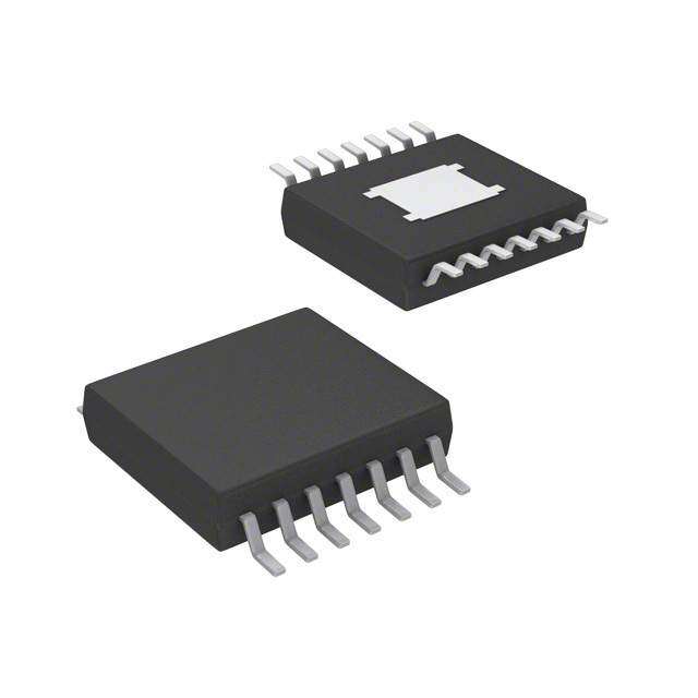
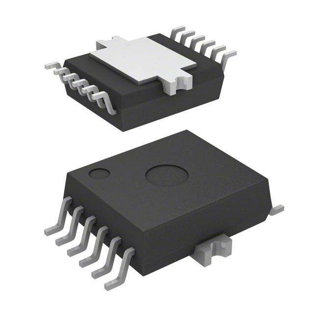
| 供应商器件封装 | 14-WSON(3x2) |
| 其它名称 | 296-30594-1 |
| 内部开关 | 是 |
| 包装 | 剪切带 (CT) |
| 商标 | Texas Instruments |
| 安装类型 | 表面贴装 |
| 安装风格 | SMD/SMT |
| 导通电阻—最大值 | 27 mOhms |
| 封装 | Reel |
| 封装/外壳 | 14-WFDFN 裸露焊盘 |
| 封装/箱体 | WSON-14 |
| 工作温度 | -40°C ~ 85°C |
| 工厂包装数量 | 3000 |
| 开关数量 | Dual |
| 开关类型 | 通用 |
| 开关配置 | N-Channel |
| 最大工作温度 | + 85 C |
| 最小工作温度 | - 40 C |
| 标准包装 | 1 |
| 比率-输入:输出 | 1:1 |
| 特性 | 负载释放 |
| 电压-负载 | 2.5 V ~ 5.5 V |
| 电压-输入 | 0.8 V ~ 5.5 V |
| 电流-输出(最大值) | 6A |
| 电流限制 | 6A |
| 电源电压-最大 | 5.5 V |
| 电源电压-最小 | 0.8 V |
| 空闲时间—最大值 | 5 us |
| 类型 | 高端 |
| 系列 | TPS22966 |
| 输入类型 | 非反相 |
| 输出数 | 2 |
| 输出类型 | N 通道 |
| 运行时间—最大值 | 2050 us |


- 商务部:美国ITC正式对集成电路等产品启动337调查
- 曝三星4nm工艺存在良率问题 高通将骁龙8 Gen1或转产台积电
- 太阳诱电将投资9.5亿元在常州建新厂生产MLCC 预计2023年完工
- 英特尔发布欧洲新工厂建设计划 深化IDM 2.0 战略
- 台积电先进制程称霸业界 有大客户加持明年业绩稳了
- 达到5530亿美元!SIA预计今年全球半导体销售额将创下新高
- 英特尔拟将自动驾驶子公司Mobileye上市 估值或超500亿美元
- 三星加码芯片和SET,合并消费电子和移动部门,撤换高东真等 CEO
- 三星电子宣布重大人事变动 还合并消费电子和移动部门
- 海关总署:前11个月进口集成电路产品价值2.52万亿元 增长14.8%


PDF Datasheet 数据手册内容提取
Product Sample & Technical Tools & Support & Folder Buy Documents Software Community TPS22966 SLVSBH4F–JUNE2012–REVISEDJULY2016 TPS22966 5.5-V, 6-A, 16-mΩ On-Resistance Dual-Channel Load Switch 1 Features 3 Description • InputVoltageRange:0.8Vto5.5V The TPS22966 is a small, low RON, dual-channel load 1 switchwithcontrolledturnon.Thedevicecontainstwo • IntegratedDual-ChannelLoadSwitch N-channel MOSFETs that can operate over an input • On-Resistance voltage range of 0.8 V to 5.5 V and can support a – R =16mΩ atV =5V(V =5V) maximum continuous current of 6 A per channel. ON IN BIAS Each switch is independently controlled by an on and – R =16mΩ atV =3.6V(V =5V) ON IN BIAS off input (ON1 and ON2), which can interface directly – RON =16mΩ atVIN =1.8V(VBIAS=5V) with low-voltage control signals. In TPS22966, a 220- • 6-AMaximumContinuousSwitchCurrentper Ω on-chip load resistor is added for quick-output Channel dischargewhenswitchisturnedoff. • LowQuiescentCurrent The TPS22966 is available in a small, space-saving – 80µA(BothChannels) 2-mm × 3-mm 14-SON package (DPU) with integrated thermal pad allowing for high power – 60µA(SingleChannel) dissipation. The device is characterized for operation • LowControlInputThresholdEnablesUseof over the free-air temperature range of –40°C to 1.2-,1.8-,2.5-,and3.3-VLogic +105°C. • ConfigurableRiseTime DeviceInformation(1) • QuickOutputDischarge(QOD)(Optional) PARTNUMBER PACKAGE BODYSIZE(NOM) • SON14-PinPackageWithThermalPad TPS22966 WSON(14) 3.00mm×2.00mm • ESDPerformanceTestedperJESD22 (1) For all available packages, see the orderable addendum at – 2-kVHBMand1-kVCDM theendofthedatasheet. 2 Applications • Ultrabook™ • NotebooksandNetbooks • TabletPCs • ConsumerElectronics • Set-topBoxesandResidentalGateways • TelecomSystems • Solid-StateDrives(SSD) ApplicationCircuit VIN1 VOUT1 Dual Power CIN ON ON1 CL Supply OFF CT1 RL or CT2 GND VBIAS Dual DC/DC converter VIN2 VOUT2 CIN ON ON2 CL OFF GND TPS22966 GND 1 An IMPORTANT NOTICE at the end of this data sheet addresses availability, warranty, changes, use in safety-critical applications, intellectualpropertymattersandotherimportantdisclaimers.PRODUCTIONDATA.
TPS22966 SLVSBH4F–JUNE2012–REVISEDJULY2016 www.ti.com Table of Contents 1 Features.................................................................. 1 8.2 FunctionalBlockDiagram.......................................15 2 Applications........................................................... 1 8.3 FeatureDescription.................................................16 3 Description............................................................. 1 8.4 DeviceFunctionalModes........................................17 4 RevisionHistory..................................................... 2 9 ApplicationandImplementation........................ 18 9.1 ApplicationInformation............................................18 5 PinConfigurationandFunctions......................... 3 9.2 TypicalApplication..................................................18 6 Specifications......................................................... 4 10 PowerSupplyRecommendations..................... 20 6.1 AbsoluteMaximumRatings......................................4 11 Layout................................................................... 20 6.2 ESDRatings..............................................................4 6.3 RecommendedOperatingConditions.......................4 11.1 LayoutGuidelines.................................................20 6.4 ThermalInformation..................................................4 11.2 LayoutExample....................................................20 6.5 ElectricalCharacteristics—V =5V.....................5 11.3 ThermalConsiderations........................................20 BIAS 6.6 ElectricalCharacteristics—V =2.5V..................6 12 DeviceandDocumentationSupport................. 22 BIAS 6.7 SwitchingCharacteristics..........................................7 12.1 DocumentationSupport........................................22 6.8 TypicalDCCharacteristics........................................8 12.2 ReceivingNotificationofDocumentationUpdates22 6.9 TypicalACCharacteristics......................................12 12.3 Trademarks...........................................................22 7 ParameterMeasurementInformation................14 12.4 ElectrostaticDischargeCaution............................22 12.5 Glossary................................................................22 8 DetailedDescription............................................ 15 13 Mechanical,Packaging,andOrderable 8.1 Overview.................................................................15 Information........................................................... 22 4 Revision History ChangesfromRevisionE(February2015)toRevisionF Page • Changed(TPS22966only)to(Optional)intheFeaturessection.......................................................................................... 1 ChangesfromRevisionD(January2015)toRevisionE Page • AddedtemperatureoperatingrangestoElectricalCharacteristics(V =5.0V)table....................................................... 5 BIAS • AddedtemperatureoperatingrangestoElectricalCharacteristics(V =2.5V)table....................................................... 6 BIAS • UpdatedgraphicsintheTypicalCharacteristicssection........................................................................................................ 8 ChangesfromRevisionC(June2013)toRevisionD Page • AddedESDRatingstable,FeatureDescriptionsection,DeviceFunctionalModes,ApplicationandImplementation section,PowerSupplyRecommendationssection,Layoutsection,DeviceandDocumentationSupportsection,and Mechanical,Packaging,andOrderableInformationsection ................................................................................................. 1 ChangesfromRevisionB(December2012)toRevisionC Page • AddedVBIAStoABSOLUTEMAXIMUMRATINGStable..................................................................................................... 4 • UpdatedSWITCHINGCHARACTERISTICMEASUREMENTINFORMATION.................................................................... 7 • UpdatedTestCircuitDiagram.............................................................................................................................................. 14 • UpdatedFunctionalBlockDiagram. .................................................................................................................................... 15 ChangesfromRevisionA(July2012)toRevisionB Page • UpdatedApplicationSchematic............................................................................................................................................. 1 2 SubmitDocumentationFeedback Copyright©2012–2016,TexasInstrumentsIncorporated ProductFolderLinks:TPS22966
TPS22966 www.ti.com SLVSBH4F–JUNE2012–REVISEDJULY2016 5 Pin Configuration and Functions DPUPackage DPUPackage 14-PinWSON 14-PinWSON TopView BottomView 1 14 14 1 VIN1 VOUT1 VOUT1 VIN1 VIN1 VOUT1 VOUT1 VIN1 ON2 CT1 CT1 ON1 VBIAS GND GND VBIAS ON2 CT2 CT2 ON2 VIN2 VOUT2 VOUT2 VIN2 VIN2 VOUT2 VOUT2 VIN2 PinFunctions PIN TYPE DESCRIPTION NO. NAME Switch1input.RecommendedvoltagerangeforthispinforoptimalR performanceis0.8VtoV . ON BIAS 1 VIN1 I PlaceanoptionaldecouplingcapacitorbetweenthispinandGNDforreduceVINdipduringturnonof thechannel.SeetheApplicationInformationsectionformoreinformation Switch1input.RecommendedvoltagerangeforthispinforoptimalR performanceis0.8VtoV . ON BIAS 2 VIN1 I PlaceanoptionaldecouplingcapacitorbetweenthispinandGNDforreduceVINdipduringturnonof thechannel.SeetheApplicationInformationsectionformoreinformation 3 ON1 I Activehighswitch1controlinput.Donotleavefloating Biasvoltage.Powersupplytothedevice.Recommendedvoltagerangeforthispinis2.5Vto5.5V. 4 VBIAS I SeetheApplicationInformationsection 5 ON2 I Activehighswitch2controlinput.Donotleavefloating Switch2input.RecommendedvoltagerangeforthispinforoptimalR performanceis0.8VtoV . ON BIAS 6 VIN2 I PlaceanoptionaldecouplingcapacitorbetweenthispinandGNDforreduceVINdipduringturnonof thechannel.SeetheApplicationInformationsectionformoreinformation Switch2input.RecommendedvoltagerangeforthispinforoptimalR performanceis0.8VtoV . ON BIAS 7 VIN2 I PlaceanoptionaldecouplingcapacitorbetweenthispinandGNDforreduceVINdipduringturnonof thechannel.SeetheApplicationInformationsectionformoreinformation 8 VOUT2 O Switch2output 9 VOUT2 O Switch2output Switch2slewratecontrol.Canbeleftfloating.Capacitorusedonthispinmudtberatedforaminimum 10 CT2 O of25Vfordesiredrisetimeperformance 11 GND — Ground Switch1slewratecontrol.Canbeleftfloating.Capacitorusedonthispinmustberatedforaminimum 12 CT1 O of25Vfordesiredrisetimeperformance 13 VOUT1 O Switch1output 14 VOUT1 O Switch1output Thermalpad(exposedcenterpad)toalleviatethermalstress.TietoGND.SeetheLayoutsectionfor — ThermalPad — layoutguidelines Copyright©2012–2016,TexasInstrumentsIncorporated SubmitDocumentationFeedback 3 ProductFolderLinks:TPS22966
TPS22966 SLVSBH4F–JUNE2012–REVISEDJULY2016 www.ti.com 6 Specifications 6.1 Absolute Maximum Ratings Overoperatingfree-airtemperaturerange(unlessotherwisenoted)(1) MIN MAX UNIT(2) V Inputvoltage –0.3 6 V IN1,2 V Outputvoltage –0.3 6 V OUT1,2 V ON-pinvoltage –0.3 6 V ON1,2 V V voltage –0.3 6 V BIAS BIAS I Maximumcontinuousswitchcurrentperchannel 6 A MAX I Maximumpulsedswitchcurrentperchannel,pulse<300µs,2%dutycycle 8 A PLS T Maximumjunctiontemperature 125 °C J T Maximumleadtemperature(10-ssolderingtime) 300 °C LEAD T Storagetemperature –65 150 °C stg (1) StressesbeyondthoselistedunderAbsoluteMaximumRatingsmaycausepermanentdamagetothedevice.Thesearestressratings only,whichdonotimplyfunctionaloperationofthedeviceattheseoranyotherconditionsbeyondthoseindicatedunderRecommended OperatingConditions.Exposuretoabsolute-maximum-ratedconditionsforextendedperiodsmayaffectdevicereliability. (2) Allvoltagevaluesarewithrespecttonetworkgroundterminal. 6.2 ESD Ratings VALUE UNIT Humanbodymodel(HBM),perANSI/ESDA/JEDECJS-001(1) ±2000 V Electrostaticdischarge V (ESD) Charged-devicemodel(CDM),perJEDECspecificationJESD22-C101(2) ±1000 (1) JEDECdocumentJEP155statesthat500-VHBMallowssafemanufacturingwithastandardESDcontrolprocess. (2) JEDECdocumentJEP157statesthat250-VCDMallowssafemanufacturingwithastandardESDcontrolprocess. 6.3 Recommended Operating Conditions MIN MAX UNIT V Inputvoltage 0.8 V V IN1,2 BIAS V Biasvoltage 2.5 5.5 V BIAS V ONvoltage 0 5.5 V ON1,2 V Outputvoltage V V OUT1,2 IN V High-levelinputvoltage,ON V =2.5Vto5.5V 1.2 5.5 V IH BIAS V Low-levelinputvoltage,ON V =2.5Vto5.5V 0 0.5 V IL BIAS C Inputcapacitor 1(1) µF IN1,2 T Operatingfree-airtemperature (2) –40 105 °C A (1) SeetheInputCapacitor(Optional)section. (2) Inapplicationswherehighpowerdissipationand/orpoorpackagethermalresistanceispresent,themaximumambienttemperaturemay havetobederated.Maximumambienttemperature[T ]isdependentonthemaximumoperatingjunctiontemperature[T ],the A(max) J(max) maximumpowerdissipationofthedeviceintheapplication[P ],andthejunction-to-ambientthermalresistanceofthepart-package D(max) intheapplication(θ ),asgivenbythefollowingequation:TA =T –(θ ×P ). JA (max) J(max) JA D(max) 6.4 Thermal Information TPS22966 THERMALMETRIC (1) DPU(WSON) UNIT 14PINS R Junction-to-ambientthermalresistance 52.3 °C/W θJA R Junction-to-case(top)thermalresistance 45.9 °C/W θJC(top) R Junction-to-boardthermalresistance 11.5 °C/W θJB ψ Junction-to-topcharacterizationparameter 0.8 °C/W JT (1) Formoreinformationabouttraditionalandnewthermalmetrics,seetheSemiconductorandICPackageThermalMetricsapplication report. 4 SubmitDocumentationFeedback Copyright©2012–2016,TexasInstrumentsIncorporated ProductFolderLinks:TPS22966
TPS22966 www.ti.com SLVSBH4F–JUNE2012–REVISEDJULY2016 Thermal Information (continued) TPS22966 THERMALMETRIC (1) DPU(WSON) UNIT 14PINS ψ Junction-to-boardcharacterizationparameter 11.4 °C/W JB R Junction-to-case(bottom)thermalresistance 6.9 °C/W θJC(bot) 6.5 Electrical Characteristics—V = 5 V BIAS Unlessotherwisenoted,thespecificationinthefollowingtableapplieswhereV =5V.TypicalvaluesareforT =25°C BIAS A (unlessotherwisenoted) PARAMETER TESTCONDITIONS T MIN TYP MAX UNIT A POWERSUPPLIESANDCURRENTS I VBIASquiescentcurrent(both IOUT1=IOUT2=0mA, –40°Cto+105°C 80 120 µA IN(VBIAS-ON) channels) V =V =V =5V IN1,2 ON1,2 BIAS I VBIASquiescentcurrent(single IOUT1=IOUT2=0mA,VON2=0V –40°Cto+105°C 60 120 µA IN(VBIAS-ON) channel) V =V =V =5V IN1,2 ON1 BIAS I V shutdowncurrent V =0V,V =0V –40°Cto+105°C 2 µA IN(VBIAS-OFF) BIAS ON1,2 OUT1,2 V =5V –40°Cto+105°C 0.5 8 IN1,2 I VIN1,2off-statesupplycurrent(per VON1,2=0V, VIN1,2=3.3V –40°Cto+105°C 0.1 3 µA IN(VIN-OFF) channel) VOUT1,2=0V VIN1,2=1.8V –40°Cto+105°C 0.07 2 V =0.8V –40°Cto+105°C 0.04 1 IN1,2 I ONpininputleakagecurrent V =5.5V –40°Cto+105°C 1 µA ON ON RESISTANCECHARACTERISTICS 25°C 16 19 V =5V –40°Cto+85°C 21 IN –40°Cto+105°C 23 25°C 16 19 V =3.3V –40°Cto+85°C 21 IN –40°Cto+105°C 23 25°C 16 19 V =1.8V –40°Cto+85°C 21 IN I =–200mA, –40°Cto+105°C 23 R ON-stateresistance(perchannel) OUT mΩ ON VBIAS=5V 25°C 16 19 V =1.5V –40°Cto+85°C 21 IN –40°Cto+105°C 23 25°C 16 19 V =1.2V –40°Cto+85°C 21 IN –40°Cto+105°C 23 25°C 16 19 V =0.8V –40°Cto+85°C 21 IN –40°Cto+105°C 23 –40°Cto+85°C 220 300 R Outputpulldownresistance V =5V,V =0V,I =15mA Ω PD IN ON OUT –40°Cto+105°C 330 Copyright©2012–2016,TexasInstrumentsIncorporated SubmitDocumentationFeedback 5 ProductFolderLinks:TPS22966
TPS22966 SLVSBH4F–JUNE2012–REVISEDJULY2016 www.ti.com 6.6 Electrical Characteristics—V = 2.5 V BIAS Unlessotherwisenoted,thespecificationinthefollowingtableapplieswhereV =2.5V.TypicalvaluesareforT =25°C BIAS A (unlessotherwisenoted) PARAMETER TESTCONDITIONS T MIN TYP MAX UNIT A POWERSUPPLIESANDCURRENTS I VBIASquiescentcurrent(both IOUT1=IOUT2=0mA, –40°Cto+85°C 32 37 µA IN(VBIAS-ON) channels) VIN1,2=VON1,2=VBIAS=2.5V –40°Cto+105°C 40 I VBIASquiescentcurrent(single IOUT1=IOUT2=0mA,VON2=0V –40°Cto+105°C 23 40 µA IN(VBIAS-ON) channel) V =V =V =2.5V IN1,2 ON1 BIAS I V shutdowncurrent V =0V,V =0V –40°Cto+105°C 2 µA IN(VBIAS-OFF) BIAS ON1,2 OUT1,2 V =2.5V –40°Cto+105°C 0.13 3 IN1,2 I VIN1,2off-statesupplycurrent(per VON1,2=0V, VIN1,2=1.8V –40°Cto+105°C 0.07 2 µA IN(VIN-OFF) channel) VOUT1,2=0V VIN1,2=1.2V –40°Cto+105°C 0.05 2 V =0.8V –40°Cto+105°C 0.04 1 IN1,2 I ONpininputleakagecurrent V =5.5V –40°Cto+105°C 1 µA ON ON RESISTANCECHARACTERISTICS 25°C 21 24 V =2.5V –40°Cto+85°C 27 IN –40°Cto+105°C 29 25°C 19 22 V =1.8V –40°Cto+85°C 25 IN –40°Cto+105°C 27 25°C 18 21 I =–200mA, R ON-stateresistance OUT V =1.5V –40°Cto+85°C 24 mΩ ON V =2.5V IN BIAS –40°Cto+105°C 26 25°C 18 21 V =1.2V –40°Cto+85°C 24 IN –40°Cto+105°C 26 25°C 17 20 V =0.8V –40°Cto+85°C 23 IN –40°Cto+105°C 25 –40°Cto+85°C 260 300 R Outputpulldownresistance V =2.5V,V =0V,I =1mA Ω PD IN ON OUT –40°Cto+105°C 330 6 SubmitDocumentationFeedback Copyright©2012–2016,TexasInstrumentsIncorporated ProductFolderLinks:TPS22966
TPS22966 www.ti.com SLVSBH4F–JUNE2012–REVISEDJULY2016 6.7 Switching Characteristics PARAMETER TESTCONDITION MIN TYP MAX UNIT V =V =V =5V,T =25ºC(unlessotherwisenoted) IN ON BIAS A t Turnontime R =10Ω,C =0.1µF,C =1000pF 1310 ON L L T t Turnofftime R =10Ω,C =0.1µF,C =1000pF 6 OFF L L T t V risetime R =10Ω,C =0.1µF,C =1000pF 1720 µs R OUT L L T t V falltime R =10Ω,C =0.1µF,C =1000pF 2 F OUT L L T t ONdelaytime R =10Ω,C =0.1µF,C =1000pF 460 D L L T V =0.8V,V =V =5V,T =25ºC(unlessotherwisenoted) IN ON BIAS A t Turnontime R =10Ω,C =0.1µF,C =1000pF 550 ON L L T t Turnofftime R =10Ω,C =0.1µF,C =1000pF 170 OFF L L T t V risetime R =10Ω,C =0.1µF,C =1000pF 325 µs R OUT L L T t V falltime R =10Ω,C =0.1µF,C =1000pF 16 F OUT L L T t ONdelaytime R =10Ω,C =0.1µF,C =1000pF 400 D L L T V =2.5V,V =5V,V =2.5V,T =25ºC(unlessotherwisenoted) IN ON BIAS A t Turnontime R =10Ω,C =0.1µF,C =1000pF 2050 ON L L T t Turnofftime R =10Ω,C =0.1µF,C =1000pF 5 OFF L L T t V risetime R =10Ω,C =0.1µF,C =1000pF 2275 µs R OUT L L T t V falltime R =10Ω,C =0.1µF,C =1000pF 2.5 F OUT L L T t ONdelaytime R =10Ω,C =0.1µF,C =1000pF 990 D L L T V =0.8V,V =5V,V =2.5V,T =25ºC(unlessotherwisenoted) IN ON BIAS A t Turnontime R =10Ω,C =0.1µF,C =1000pF 1300 ON L L T t Turnofftime R =10Ω,C =0.1µF,C =1000pF 130 OFF L L T t V risetime R =10Ω,C =0.1µF,C =1000pF 875 µs R OUT L L T t V falltime R =10Ω,C =0.1µF,C =1000pF 16 F OUT L L T t ONdelaytime R =10Ω,C =0.1µF,C =1000pF 870 D L L T Copyright©2012–2016,TexasInstrumentsIncorporated SubmitDocumentationFeedback 7 ProductFolderLinks:TPS22966
TPS22966 SLVSBH4F–JUNE2012–REVISEDJULY2016 www.ti.com 6.8 Typical DC Characteristics 120 100 -40qC -40qC 25qC 90 25qC 100 105qC 105qC 80 A) A) nt (P 80 nt (P 70 e e Curr 60 Curr 60 nt nt 50 e e c c es 40 es 40 ui ui Q Q 30 20 20 0 10 2.5 3 3.5 4 4.5 5 5.5 2.5 3 3.5 4 4.5 5 5.5 Bias Voltage (V) Bias Voltage (V) D001 D002 V =V =V V =V =5V V =Open V =V =V V =V =5V V =Open IN1 IN2 BIAS ON1 ON2 OUT IN1 IN2 BIAS ON1 ON2 OUT Figure1.QuiescentCurrentvsBiasVoltage Figure2.QuiescentCurrentvsBiasVoltage BothChannels SingleChannel 1.2 0.3 -40qC -40qC 1.1 25qC 25qC Current (A)P 000...7891 105qC N Current (A)P 000..12.255 105qC Shutdown 000...456 Off-State VI 0.1 0.05 0.3 0.2 0 2.5 3 3.5 4 4.5 5 5.5 0.8 1.2 1.6 2 2.4 2.8 3.2 3.6 4 4.4 4.8 5.2 Bias Voltage (V) Input Voltage (V) D003 D004 V =V =V V =V =0V V =0V V =5V V =0V V =0V IN1 IN2 BIAS ON1 ON2 OUT BIAS ON OUT Figure3.ShutdownCurrentvsBiasVoltage Figure4.Off-StateVINCurrentvsInputVoltage BothChannels SingleChannel 28 22 VIN = 0.8 V VIN = 0.8 V 26 VIN = 1.2 V 21 VIN = 1.2 V VIN = 1.5 V 20 VIN = 1.5 V 24 VIN = 1.8 V VIN = 2.5 V :) VIN = 2.5 V :) 19 VIN = 3.3 V e (m 22 e (m 18 VIN = 5 V c c n n a 20 a 17 st st Resi 18 Resi 16 On- On- 15 16 14 14 13 12 12 -45 -20 5 30 55 80 105 -45 -20 5 30 55 80 105 Temperature (qC) Temperature (qC) D005 D006 V =2.5V I =–200mA V =5V I =–200mA BIAS OUT BIAS OUT Figure5.On-ResistancevsTemperature Figure6.On-ResistancevsTemperature SingleChannel SingleChannel 8 SubmitDocumentationFeedback Copyright©2012–2016,TexasInstrumentsIncorporated ProductFolderLinks:TPS22966
TPS22966 www.ti.com SLVSBH4F–JUNE2012–REVISEDJULY2016 Typical DC Characteristics (continued) 26 23 -40qC -40qC 24 25qC 22 25qC 105qC 21 105qC :) 22 :) 20 e (m 20 e (m 19 nc nc 18 a 18 a st st 17 si si Re 16 Re 16 n- n- O 14 O 15 14 12 13 10 12 0.8 1 1.2 1.4 1.6 1.8 2 2.2 2.4 2.6 0.8 1.2 1.6 2 2.4 2.8 3.2 3.6 4 4.4 4.8 5.2 Input Voltage (V) Input Voltage (V) D007 D008 V =2.5V I =–200mA V =5V I =–200mA BIAS OUT BIAS OUT Figure7.On-ResistancevsInputVoltage Figure8.On-ResistancevsInputVoltage SingleChannel SingleChannel 22.5 250 VBIAS = 2.5 V -40qC 22 VBIAS = 3.3 V 25qC VBIAS = 3.6 V 245 105qC 21.5 VBIAS = 4.2 V :) :Resistance (m) 2022.501 VVBBIIAASS == 55 .V5 V wn Resistance ( 223450 n- do 230 O 19.5 Pull 225 19 18.5 220 0.8 1.2 1.6 2 2.4 2.8 3.2 3.6 4 4.4 4.8 5.2 5.6 0.8 1.2 1.6 2 2.4 2.8 3.2 3.6 4 4.4 4.8 5.2 Input Voltage} (V) Input Voltage (V) D009 D010 T =25°C V =5V I =1mA V =0V A BIAS OUT ON Figure9.On-ResistancevsInputVoltage Figure10.PulldownResistancevsInputVoltage SingleChannel SingleChannel 2.5 1800 1600 2 Voltage (V) 1.5 Time (s)P 11240000 ut 1 ay 1000 utp VBIAS = 2.5 V Del O VBIAS = 3.3 V 800 VBIAS = 3.6 V -40qC 0.5 VBIAS = 4.2 V 25qC VBIAS = 5 V 600 85qC VBIAS = 5.5 V 105qC 0 400 0.5 1 1.5 2 2.5 0.8 1 1.2 1.4 1.6 1.8 2 2.2 2.4 2.6 ON Voltage (V) Input Voltage (V) D011 D012 T =25°C V =2.5V CT=1nF A BIAS Figure11.OutputVoltagevsONVoltage Figure12.DelayTimevsInputVoltage SingleChannel Copyright©2012–2016,TexasInstrumentsIncorporated SubmitDocumentationFeedback 9 ProductFolderLinks:TPS22966
TPS22966 SLVSBH4F–JUNE2012–REVISEDJULY2016 www.ti.com Typical DC Characteristics (continued) 900 20 -40qC 18 25qC 800 16 85qC 105qC 14 Delay Time (s)P 567000000 Fall Time (s)P 11802 6 4 400 -40qC 85qC 2 25qC 105qC 300 0 0.8 1.2 1.6 2 2.4 2.8 3.2 3.6 4 4.4 4.8 5.2 0.8 1 1.2 1.4 1.6 1.8 2 2.2 2.4 2.6 Input Voltage (V) Input Voltage (V) D013 D014 V =5V CT=1nF V =2.5V CT=1nF BIAS BIAS Figure13.DelayTimevsInputVoltage Figure14.FallTimevsInputVoltage 25 180 -40qC -40qC 25qC 160 25qC 20 8150q5CqC 140 81505qCqC e (s)P 15 me (s)P 110200 m Ti Fall Ti 10 urnoff 6800 T 5 40 20 0 0 0.8 1.2 1.6 2 2.4 2.8 3.2 3.6 4 4.4 4.8 5.2 0.8 1 1.2 1.4 1.6 1.8 2 2.2 2.4 2.6 Input Voltage (V) Input Voltage (V) D015 D016 V =5V CT=1nF V =2.5V CT=1nF BIAS BIAS Figure15.FallTimevsInputVoltage Figure16.TurnoffTimevsInputVoltage 250 3500 -40qC -40qC 25qC 25qC 200 85qC 3000 85qC 105qC 105qC s) s) P P e ( 150 e ( 2500 m m Ti Ti noff 100 non 2000 ur ur T T 50 1500 0 1000 0.8 1.2 1.6 2 2.4 2.8 3.2 3.6 4 4.4 4.8 5.2 0.8 1 1.2 1.4 1.6 1.8 2 2.2 2.4 2.6 Input Voltage (V) Input Voltage (V) D017 D018 V =5V CT=1nF V =2.5V CT=1nF BIAS BIAS Figure17.TurnoffTimevsInputVoltage Figure18.TurnonTimevsInputVoltage 10 SubmitDocumentationFeedback Copyright©2012–2016,TexasInstrumentsIncorporated ProductFolderLinks:TPS22966
TPS22966 www.ti.com SLVSBH4F–JUNE2012–REVISEDJULY2016 Typical DC Characteristics (continued) 2000 3500 -40qC -40qC 1800 25qC 25qC 85qC 3000 85qC 1600 105qC 105qC me (s)P 1400 e (s)P 2500 on Ti 1200 e Tim 2000 urn 1000 Ris 1500 T 800 1000 600 400 500 0.8 1.2 1.6 2 2.4 2.8 3.2 3.6 4 4.4 4.8 5.2 0.8 1 1.2 1.4 1.6 1.8 2 2.2 2.4 2.6 Input Voltage (V) Input Voltage (V) D019 D020 V =5V CT=1nF V =2.5V CT=1nF BIAS BIAS Figure19.TurnonTimevsInputVoltage Figure20.RiseTimevsInputVoltage 2750 3500 -40qC -40qC 25qC 25qC 2250 85qC 3000 85qC 105qC 105qC s) s) 2500 P 1750 P e ( e ( m m 2000 Ti Ti se 1250 se Ri Ri 1500 750 1000 250 500 0.8 1.2 1.6 2 2.4 2.8 3.2 3.6 4 4.4 4.8 5.2 2.5 2.75 3 3.25 3.5 3.75 4 4.25 4.5 4.75 5 Input Voltage (V) Input Voltage (V) D021 D022 V =5V CT=1nF V =2.5V CT=1nF BIAS IN Figure21.RiseTimevsInputVoltage(V =5V,CT=1 Figure22.RiseTimevsBiasVoltage BIAS nF) Copyright©2012–2016,TexasInstrumentsIncorporated SubmitDocumentationFeedback 11 ProductFolderLinks:TPS22966
TPS22966 SLVSBH4F–JUNE2012–REVISEDJULY2016 www.ti.com 6.9 Typical AC Characteristics AtT =25ºC,CT=1nF A V =0.8V V =2.5V C =1µF V =0.8V V =5V C =1µF IN BIAS IN IN BIAS IN C =0.1µF R =10Ω C =0.1µF R =10Ω L L L L Figure23.TurnonResponseTime Figure24.TurnonResponseTime V =2.5V V =2.5V C =1µF V =5V V =5V C =1µF IN BIAS IN IN BIAS IN C =0.1µF R =10Ω C =0.1µF R =10Ω L L L L Figure25.TurnonResponseTime Figure26.TurnonResponseTime V =0.8V V =2.5V C =1µF V =0.8V V =5V C =1µF IN BIAS IN IN BIAS IN C =0.1µF R =10Ω C =0.1µF R =10Ω L L L L Figure27.TurnoffResponseTime Figure28.TurnoffResponseTime 12 SubmitDocumentationFeedback Copyright©2012–2016,TexasInstrumentsIncorporated ProductFolderLinks:TPS22966
TPS22966 www.ti.com SLVSBH4F–JUNE2012–REVISEDJULY2016 Typical AC Characteristics (continued) AtT =25ºC,CT=1nF A V =2.5V V =2.5V C =1µF V =5V V =5V C =1µF IN BIAS IN IN BIAS IN C =0.1µF R =10Ω C =0.1µF R =10Ω L L L L Figure29.TurnoffResponseTime Figure30.TurnoffResponseTime Copyright©2012–2016,TexasInstrumentsIncorporated SubmitDocumentationFeedback 13 ProductFolderLinks:TPS22966
TPS22966 SLVSBH4F–JUNE2012–REVISEDJULY2016 www.ti.com 7 Parameter Measurement Information V V IN OUT C = 1(cid:29)F CTx IN ON + ON CL (A) - R L OFF VBIAS GND TPS22966 GND GND Single channel shown for clarity. Test Circuit V ON 50% 50% t t t f t OFF r ON V 90% 90% VOUT 50% 50% OUT 10% 10% 10% t D t and t Waveforms ON OFF (A) Rise and fall times of the control signal is 100 ns. Figure31. TestCircuitandt -t Waveforms ON OFF 14 SubmitDocumentationFeedback Copyright©2012–2016,TexasInstrumentsIncorporated ProductFolderLinks:TPS22966
TPS22966 www.ti.com SLVSBH4F–JUNE2012–REVISEDJULY2016 8 Detailed Description 8.1 Overview The TPS22966 device is a dual-channel, 6-A load switch in a 14-terminal SON package. To reduce the voltage drop in high current rails, the device implements an low resistance N-channel MOSFET. The device has a programmableslewrateforapplicationsthatrequirespecificrise-time. The device has very low leakage current during off state. This prevents downstream circuits from pulling high standby current from the supply. Integrated control logic, driver, power supply, and output discharge FET eliminatestheneedforanyexternalcomponents,whichreducessolutionsizeandbillofmaterials(BOM)count. 8.2 Functional Block Diagram VIN1 Control ON1 Logic CT1 VOUT1 GND VBIAS Charge Pump VOUT2 CT2 Control ON2 Logic VIN2 Copyright©2012–2016,TexasInstrumentsIncorporated SubmitDocumentationFeedback 15 ProductFolderLinks:TPS22966
TPS22966 SLVSBH4F–JUNE2012–REVISEDJULY2016 www.ti.com 8.3 Feature Description 8.3.1 ONandOFFControl The ON pins control the state of the switch. Asserting ON high enables the switch. ON is active high and has a low threshold, making it capable of interfacing with low-voltage signals. The ON pin is compatible with standard GPIO logic threshold. It can be used with any microcontroller with 1.2-V or higher GPIO voltage. This pin cannot beleftfloatingandmustbetiedeitherhighorlowforproperfunctionality. 8.3.2 InputCapacitor(Optional) To limit the voltage drop on the input supply caused by transient inrush currents when the switch turns on into a dischargedloadcapacitor,acapacitorneedstobeplacedbetweenVINandGND.A1-µFceramiccapacitor,C , IN placed close to the pins, is usually sufficient. Higher values of C can be used to further reduce the voltage drop IN during high-current application. When switching heavy loads, it is recommended to have an input capacitor about 10timeshigherthantheoutputcapacitortoavoidexcessivevoltagedrop. 8.3.3 OutputCapacitor(Optional) Due to the integrated body diode in the NMOS switch, a C greater than C is highly recommended. A C IN L L greater than C can cause V to exceed V when the system supply is removed. This could result in current IN OUT IN flow through the body diode from VOUT to VIN. A C to C ratio of 10 to 1 is recommended for minimizing V IN L IN dip caused by inrush currents during startup, however a 10 to 1 ratio for capacitance is not required for proper functionality of the device. A ratio smaller than 10 to 1 (such as 1 to 1) could cause slightly more V dip upon IN turn-on due to inrush currents. This can be mitigated by increasing the capacitance on the CT pin for a longer risetime(seeFigure4). 8.3.4 V andV VoltageRange IN BIAS ForoptimalR performance,makesureV ≤V .ThedeviceisstillfunctionalifV > V butitexhibitsR ON IN BIAS IN BIAS ON greater than what is listed in the Electrical Characteristics table. See Figure 32 for an example of a typical device. Notice the increasing R as V exceeds V voltage. Make sure to never exceed the maximum ON IN BIAS voltageratingforV andV . IN BIAS 52 VBIAS = 2.5 V VBIAS = 3.3 V 47 VBIAS = 3.6 V VBIAS = 4.2 V :) 42 VBIAS = 5 V m VBIAS = 5.5 V ce ( 37 n a st si 32 e R On- 27 22 17 0.8 1.2 1.6 2 2.4 2.8 3.2 3.6 4 4.4 4.8 5.2 5.6 Input Voltage} (V) D050 V >V I =–200mA IN BIAS OUT Figure32. On-ResistancevsInputVoltage SingleChannel 16 SubmitDocumentationFeedback Copyright©2012–2016,TexasInstrumentsIncorporated ProductFolderLinks:TPS22966
TPS22966 www.ti.com SLVSBH4F–JUNE2012–REVISEDJULY2016 8.4 Device Functional Modes Table1liststheTPS22966functions. Table1.FunctionsTable ONx VINxtoVOUTx VOUTxtoGND L Off On H On Off Copyright©2012–2016,TexasInstrumentsIncorporated SubmitDocumentationFeedback 17 ProductFolderLinks:TPS22966
TPS22966 SLVSBH4F–JUNE2012–REVISEDJULY2016 www.ti.com 9 Application and Implementation NOTE Information in the following applications sections is not part of the TI component specification, and TI does not warrant its accuracy or completeness. TI’s customers are responsible for determining suitability of components for their purposes. Customers should validateandtesttheirdesignimplementationtoconfirmsystemfunctionality. 9.1 Application Information This application demonstrates how the TPS22966 can be used to limit inrush current when powering on downstreammodules. 9.2 Typical Application VIN1 VOUT1 PDouwaelr CIN ON ON1 CL Supply OFF CT1 RL or CT2 GND VBIAS Dual DC/DC converter VIN2 VOUT2 CIN ON ON2 CL OFF GND TPS22966 GND Figure33. TypicalApplicationCircuit 9.2.1 DesignRequirements Table2showstheTPS22966desginparameters. Table2.DesignParameters DESIGNPARAMETER VALUE Inputvoltage 3.3V Biasvoltage 5V Loadcapacitance(C ) 22µF L Maximumacceptableinrushcurrent 400mA 9.2.2 DetailedDesignProcedure When the switch is enabled, the output capacitors must be charged up from 0 V to the set value (3.3 V in this example).Thischargearrivesintheformofinrushcurrent.InrushcurrentcanbecalculatedusingEquation1. InrushCurrent=C×dV/dt where • Cistheoutputcapacitance • dVistheoutputvoltage • dtistherisetime (1) The TPS22966 offers adjustable rise time for VOUT. This feature allows the user to control the inrush current duringturnon.TheappropriaterisetimecanbecalculatedusingTable2andEquation1 asshowninEquation2. 400mA=22μF×3.3V/dt (2) dt=181.5μs (3) 18 SubmitDocumentationFeedback Copyright©2012–2016,TexasInstrumentsIncorporated ProductFolderLinks:TPS22966
TPS22966 www.ti.com SLVSBH4F–JUNE2012–REVISEDJULY2016 To ensure an inrush current of less than 400 mA, choose a CT value that yields a rise time of more than 181.5 μs. See the oscilloscope captures in the Application Curves section for an example of how the CT capacitor can beusedtoreduceinrushcurrent. 9.2.2.1 AdjustableRiseTime A capacitor to GND on the CTx pins sets the slew rate for each channel. To ensure desired performance, a capacitor with a minimum voltage rating of 25 V must be used on the CTx pin. An approximate formula for the relationship between CTx and slew rate is given in Equation 4. Equation 4 accounts for 10% to 90% measurementonV anddoesNOT applyforCTx=0pF.(UseTable3todeterminerisetimesforwhenCTx= OUT 0pF). SR =0.32´CT+13.7 where • SRistheslewrate(inµs/V) • CTisthecapacitancevalueontheCTxpin(inpF) • Theunitsfortheconstant13.7isinµs/V. (4) Rise time can be calculated by multiplying the input voltage by the slew rate. Table 3 shows rise time values measured on a typical device. Rise times shown in Table 3 are only valid for the power-up sequence where V IN andV arealreadyinsteadystatecondition,andtheONpinisassertedhigh. BIAS Table3.RiseTimeValues RISETIME(µs)10%-90%,C =0.1µF,C =1µF,R =10Ω L IN L CTx(pF) (1)5V 3.3V 1.8V 1.5V 1.2V 1.05V 0.8V 0 124 88 63 60 53 49 42 220 481 323 193 166 143 133 109 470 855 603 348 299 251 228 175 1000 1724 1185 670 570 469 411 342 2200 3328 2240 1308 1088 893 808 650 4700 7459 4950 2820 2429 1920 1748 1411 10000 16059 10835 6040 5055 4230 3770 3033 (1) TYPICALVALUESat25°C,V =5V,25VX7R10%CERAMICCAP. BIAS 9.2.3 ApplicationCurves V =5V V =3.3V C =22μF V =5V V =3.3V C =22μF BIAS IN L BIAS IN L Figure34.InrushCurrentwithCT=0pF Figure35.InrushCurrentwithCT=220pF Copyright©2012–2016,TexasInstrumentsIncorporated SubmitDocumentationFeedback 19 ProductFolderLinks:TPS22966
TPS22966 SLVSBH4F–JUNE2012–REVISEDJULY2016 www.ti.com 10 Power Supply Recommendations ThedeviceisdesignedtooperatefromaVBIASrangeof2.5Vto5.5VandaVINrangeof0.8VtoVBIAS. 11 Layout 11.1 Layout Guidelines For best performance, all traces must be as short as possible. To be most effective, the input and output capacitors must be placed close to the device to minimize the effects that parasitic trace inductances may have on normal operation. Using wide traces for VIN, VOUT, and GND helps minimize the parasitic electrical effects alongwithminimizingthecasetoambientthermalimpedance. 11.2 Layout Example Notice the thermal vias located under the exposed thermal pad of the device. This allows for thermal diffusion awayfromthedevice. VOUT1 capacitor VIN1 capacitor CT1 capacitor Thermal relief vias VIN2 capacitor CT2 capacitor VOUT2 capacitor Figure36. PCBLayoutExample 11.3 Thermal Considerations The maximum IC junction temperature must be restricted to 125°C under normal operating conditions. To calculate the maximum allowable power dissipation, P for a given output current and ambient temperature, D(max) useEquation5: T -T P = J(max) A D(max) θ JA where • P isthemaximumallowablepowerdissipation D(max) • T isthemaximumallowablejunctiontemperature(125°CfortheTPS22966) J(max) • T istheambienttemperatureofthedevice A 20 SubmitDocumentationFeedback Copyright©2012–2016,TexasInstrumentsIncorporated ProductFolderLinks:TPS22966
TPS22966 www.ti.com SLVSBH4F–JUNE2012–REVISEDJULY2016 Thermal Considerations (continued) • θ isthejunctiontoairthermalimpedance.SeetheThermalInformationsection.Thisparameterishighly JA dependentuponboardlayout. (5) Copyright©2012–2016,TexasInstrumentsIncorporated SubmitDocumentationFeedback 21 ProductFolderLinks:TPS22966
TPS22966 SLVSBH4F–JUNE2012–REVISEDJULY2016 www.ti.com 12 Device and Documentation Support 12.1 Documentation Support 12.1.1 RelatedDocumentation Forrelateddocumentationseethefollowing: • TPS22966DualChannelLoadSwitchinParallelConfiguration,SLVA585A • BasicsofLoadSwitches,SLVA652 • ManagingInrushCurrent,SLVA670A • QuiescentCurrentvsShutdownCurrentforLoadSwitchPowerConsumption,SLVA757 • UsingtheTPS22966EVM-007,SLVU757A • LoadSwitchThermalConsiderations,SLVUA74 12.2 Receiving Notification of Documentation Updates To receive notification of documentation updates, navigate to the device product folder on ti.com. In the upper right corner, click on Alert me to register and receive a weekly digest of any product information that has changed.Forchangedetails,reviewtherevisionhistoryincludedinanyreviseddocument. 12.3 Trademarks UltrabookisatrademarkofIntel. Allothertrademarksarethepropertyoftheirrespectiveowners. 12.4 Electrostatic Discharge Caution This integrated circuit can be damaged by ESD. Texas Instruments recommends that all integrated circuits be handled with appropriateprecautions.Failuretoobserveproperhandlingandinstallationprocedurescancausedamage. ESDdamagecanrangefromsubtleperformancedegradationtocompletedevicefailure.Precisionintegratedcircuitsmaybemore susceptibletodamagebecauseverysmallparametricchangescouldcausethedevicenottomeetitspublishedspecifications. 12.5 Glossary SLYZ022—TIGlossary. Thisglossarylistsandexplainsterms,acronyms,anddefinitions. 13 Mechanical, Packaging, and Orderable Information The following pages include mechanical, packaging, and orderable information. This information is the most current data available for the designated devices. This data is subject to change without notice and revision of thisdocument.Forbrowser-basedversionsofthisdatasheet,refertotheleft-handnavigation. 22 SubmitDocumentationFeedback Copyright©2012–2016,TexasInstrumentsIncorporated ProductFolderLinks:TPS22966
PACKAGE OPTION ADDENDUM www.ti.com 6-Feb-2020 PACKAGING INFORMATION Orderable Device Status Package Type Package Pins Package Eco Plan Lead/Ball Finish MSL Peak Temp Op Temp (°C) Device Marking Samples (1) Drawing Qty (2) (6) (3) (4/5) TPS22966DPUR ACTIVE WSON DPU 14 3000 Green (RoHS NIPDAU Level-2-260C-1 YEAR -40 to 105 RB966 & no Sb/Br) TPS22966DPUT ACTIVE WSON DPU 14 250 Green (RoHS NIPDAU Level-2-260C-1 YEAR -40 to 105 RB966 & no Sb/Br) (1) The marketing status values are defined as follows: ACTIVE: Product device recommended for new designs. LIFEBUY: TI has announced that the device will be discontinued, and a lifetime-buy period is in effect. NRND: Not recommended for new designs. Device is in production to support existing customers, but TI does not recommend using this part in a new design. PREVIEW: Device has been announced but is not in production. Samples may or may not be available. OBSOLETE: TI has discontinued the production of the device. (2) RoHS: TI defines "RoHS" to mean semiconductor products that are compliant with the current EU RoHS requirements for all 10 RoHS substances, including the requirement that RoHS substance do not exceed 0.1% by weight in homogeneous materials. Where designed to be soldered at high temperatures, "RoHS" products are suitable for use in specified lead-free processes. TI may reference these types of products as "Pb-Free". RoHS Exempt: TI defines "RoHS Exempt" to mean products that contain lead but are compliant with EU RoHS pursuant to a specific EU RoHS exemption. Green: TI defines "Green" to mean the content of Chlorine (Cl) and Bromine (Br) based flame retardants meet JS709B low halogen requirements of <=1000ppm threshold. Antimony trioxide based flame retardants must also meet the <=1000ppm threshold requirement. (3) MSL, Peak Temp. - The Moisture Sensitivity Level rating according to the JEDEC industry standard classifications, and peak solder temperature. (4) There may be additional marking, which relates to the logo, the lot trace code information, or the environmental category on the device. (5) Multiple Device Markings will be inside parentheses. Only one Device Marking contained in parentheses and separated by a "~" will appear on a device. If a line is indented then it is a continuation of the previous line and the two combined represent the entire Device Marking for that device. (6) Lead/Ball Finish - Orderable Devices may have multiple material finish options. Finish options are separated by a vertical ruled line. Lead/Ball Finish values may wrap to two lines if the finish value exceeds the maximum column width. Important Information and Disclaimer:The information provided on this page represents TI's knowledge and belief as of the date that it is provided. TI bases its knowledge and belief on information provided by third parties, and makes no representation or warranty as to the accuracy of such information. Efforts are underway to better integrate information from third parties. TI has taken and continues to take reasonable steps to provide representative and accurate information but may not have conducted destructive testing or chemical analysis on incoming materials and chemicals. TI and TI suppliers consider certain information to be proprietary, and thus CAS numbers and other limited information may not be available for release. In no event shall TI's liability arising out of such information exceed the total purchase price of the TI part(s) at issue in this document sold by TI to Customer on an annual basis. Addendum-Page 1
PACKAGE OPTION ADDENDUM www.ti.com 6-Feb-2020 OTHER QUALIFIED VERSIONS OF TPS22966 : •Automotive: TPS22966-Q1 NOTE: Qualified Version Definitions: •Automotive - Q100 devices qualified for high-reliability automotive applications targeting zero defects Addendum-Page 2
PACKAGE MATERIALS INFORMATION www.ti.com 21-Oct-2018 TAPE AND REEL INFORMATION *Alldimensionsarenominal Device Package Package Pins SPQ Reel Reel A0 B0 K0 P1 W Pin1 Type Drawing Diameter Width (mm) (mm) (mm) (mm) (mm) Quadrant (mm) W1(mm) TPS22966DPUR WSON DPU 14 3000 180.0 8.4 2.25 3.25 1.05 4.0 8.0 Q1 TPS22966DPUR WSON DPU 14 3000 180.0 8.4 2.25 3.25 1.05 4.0 8.0 Q1 TPS22966DPUT WSON DPU 14 250 180.0 8.4 2.25 3.25 1.05 4.0 8.0 Q1 PackMaterials-Page1
PACKAGE MATERIALS INFORMATION www.ti.com 21-Oct-2018 *Alldimensionsarenominal Device PackageType PackageDrawing Pins SPQ Length(mm) Width(mm) Height(mm) TPS22966DPUR WSON DPU 14 3000 210.0 185.0 35.0 TPS22966DPUR WSON DPU 14 3000 210.0 185.0 35.0 TPS22966DPUT WSON DPU 14 250 210.0 185.0 35.0 PackMaterials-Page2
None
None
None
IMPORTANTNOTICEANDDISCLAIMER TI PROVIDES TECHNICAL AND RELIABILITY DATA (INCLUDING DATASHEETS), DESIGN RESOURCES (INCLUDING REFERENCE DESIGNS), APPLICATION OR OTHER DESIGN ADVICE, WEB TOOLS, SAFETY INFORMATION, AND OTHER RESOURCES “AS IS” AND WITH ALL FAULTS, AND DISCLAIMS ALL WARRANTIES, EXPRESS AND IMPLIED, INCLUDING WITHOUT LIMITATION ANY IMPLIED WARRANTIES OF MERCHANTABILITY, FITNESS FOR A PARTICULAR PURPOSE OR NON-INFRINGEMENT OF THIRD PARTY INTELLECTUAL PROPERTY RIGHTS. These resources are intended for skilled developers designing with TI products. You are solely responsible for (1) selecting the appropriate TI products for your application, (2) designing, validating and testing your application, and (3) ensuring your application meets applicable standards, and any other safety, security, or other requirements. These resources are subject to change without notice. TI grants you permission to use these resources only for development of an application that uses the TI products described in the resource. Other reproduction and display of these resources is prohibited. No license is granted to any other TI intellectual property right or to any third party intellectual property right. TI disclaims responsibility for, and you will fully indemnify TI and its representatives against, any claims, damages, costs, losses, and liabilities arising out of your use of these resources. TI’s products are provided subject to TI’s Terms of Sale (www.ti.com/legal/termsofsale.html) or other applicable terms available either on ti.com or provided in conjunction with such TI products. TI’s provision of these resources does not expand or otherwise alter TI’s applicable warranties or warranty disclaimers for TI products. Mailing Address: Texas Instruments, Post Office Box 655303, Dallas, Texas 75265 Copyright © 2020, Texas Instruments Incorporated