ICGOO在线商城 > 集成电路(IC) > 数据采集 - 数字电位器 > MCP41HV51-503E/ST

 Datasheet下载
- 型号: MCP41HV51-503E/ST
- 制造商: Microchip
- 库位|库存: xxxx|xxxx
- 要求:
| 数量阶梯 | 香港交货 | 国内含税 |
| +xxxx | $xxxx | ¥xxxx |
查看当月历史价格
查看今年历史价格
MCP41HV51-503E/ST产品简介:
ICGOO电子元器件商城为您提供MCP41HV51-503E/ST由Microchip设计生产,在icgoo商城现货销售,并且可以通过原厂、代理商等渠道进行代购。 MCP41HV51-503E/ST价格参考。MicrochipMCP41HV51-503E/ST封装/规格:数据采集 - 数字电位器, Digital Potentiometer 50k Ohm 1 Circuit 256 Taps SPI Interface 14-TSSOP。您可以下载MCP41HV51-503E/ST参考资料、Datasheet数据手册功能说明书,资料中有MCP41HV51-503E/ST 详细功能的应用电路图电压和使用方法及教程。
MCP41HV51-503E/ST 是由 Microchip Technology 生产的一款数字电位器,属于数据采集系列中的数字电位器类别。它是一种可编程的电阻器件,能够替代传统的机械电位器,在需要动态调整电阻值的应用中提供更高的稳定性和可靠性。

以下是 MCP41HV51-503E/ST 的主要应用场景:

1. 音频设备音量控制
   数字电位器常用于音频设备(如音响、耳机放大器等)中实现音量调节功能。相比传统机械电位器,MCP41HV51 提供更长的使用寿命和更高的精度。

2. 电源管理
   在电源管理系统中,该器件可用于动态调整电压分压器或反馈网络的电阻值,从而实现对输出电压的精确控制。例如,稳压电源或 DC-DC 转换器中的参考电压调节。

3. 工业自动化与控制
   在工业控制系统中,MCP41HV51 可用于传感器信号调理电路,通过调整增益或偏移来优化信号处理性能。此外,它还可以用于 PID 控制器的参数调节。

4. 医疗设备
   该数字电位器适用于医疗设备中的信号调节和校准功能,例如心率监测仪、血压计等。其高可靠性和稳定性确保了设备的长期运行性能。

5. 消费电子产品
   在消费电子产品中,MCP41HV51 可用于亮度调节、对比度调节等功能,例如 LCD 显示屏的背光亮度控制。

6. 汽车电子
   在汽车电子领域,该器件可用于座椅位置记忆、后视镜角度调节、车内灯光亮度控制等需要动态电阻调整的应用场景。

7. 测试与测量设备
   数字电位器在测试仪器(如示波器、万用表等)中用于校准和调整功能,确保测量结果的准确性。

MCP41HV51-503E/ST 具有高达 5V 的工作电压范围和 10kΩ 的标称阻值,支持 SPI 接口通信,便于集成到各种嵌入式系统中。其小型化封装(SOT-23)也使其非常适合空间受限的设计环境。
| 参数 | 数值 |
| 产品目录 | 集成电路 (IC)半导体 |
| 描述 | IC DGTL POT 8BIT 50K 14TSSOP数字电位计 IC 8-bit volatile Potentiometer 50kohm |
| 产品分类 | |
| 品牌 | Microchip Technology |
| 产品手册 | |
| 产品图片 |
|
| 产品系列 | 数字电位计 IC,Microchip Technology MCP41HV51-503E/ST- |
| mouser_ship_limit | 该产品可能需要其他文件才能进口到中国。 |
| 数据手册 | http://www.microchip.com/mymicrochip/filehandler.aspx?ddocname=en561493 |
| 产品型号 | MCP41HV51-503E/ST |
| POT数量 | Single |
| rohs | 无铅 / 符合限制有害物质指令(RoHS)规范要求 |
| 产品种类 | 数字电位计 IC |
| 供应商器件封装 | 14-TSSOP |
| 包装 | 管件 |
| 商标 | Microchip Technology |
| 存储器类型 | 易失 |
| 安装类型 | 表面贴装 |
| 安装风格 | SMD/SMT |
| 封装 | Tube |
| 封装/外壳 | 14-TSSOP(0.173",4.40mm 宽) |
| 封装/箱体 | TSSOP-14 |
| 工作温度 | -40°C ~ 125°C |
| 工作电源电压 | 1.8 to 5.5 V |
| 工厂包装数量 | 96 |
| 弧刷存储器 | Volatile |
| 抽头 | 256 |
| 接口 | SPI 串行 |
| 描述/功能 | Digital potentiometer with SPI serial interface and volatile memory |
| 数字接口 | SPI |
| 最大工作温度 | + 125 C |
| 最小工作温度 | - 40 C |
| 标准包装 | 96 |
| 每POT分接头 | 256 |
| 温度系数 | - |
| 电压-电源 | - |
| 电源电压-最大 | 5.5 V |
| 电源电压-最小 | 1.8 V |
| 电源电流 | 45 uA |
| 电路数 | 1 |
| 电阻 | 50 kOhms |
| 电阻(Ω) | 50k |
| 缓冲刷 | Non Buffered |


- 商务部:美国ITC正式对集成电路等产品启动337调查
- 曝三星4nm工艺存在良率问题 高通将骁龙8 Gen1或转产台积电
- 太阳诱电将投资9.5亿元在常州建新厂生产MLCC 预计2023年完工
- 英特尔发布欧洲新工厂建设计划 深化IDM 2.0 战略
- 台积电先进制程称霸业界 有大客户加持明年业绩稳了
- 达到5530亿美元!SIA预计今年全球半导体销售额将创下新高
- 英特尔拟将自动驾驶子公司Mobileye上市 估值或超500亿美元
- 三星加码芯片和SET,合并消费电子和移动部门,撤换高东真等 CEO
- 三星电子宣布重大人事变动 还合并消费电子和移动部门
- 海关总署:前11个月进口集成电路产品价值2.52万亿元 增长14.8%


PDF Datasheet 数据手册内容提取
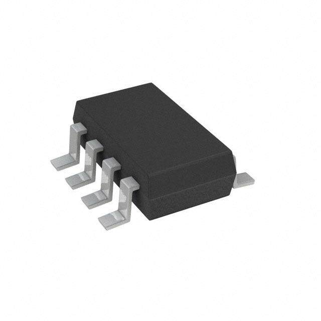
MCP41HVX1 7/8-Bit Single, +36V (±18V) Digital POT with SPI Serial Interface and Volatile Memory Package Types Features MCP41HVX1 Single Potentiometer • High-Voltage Analog Support: - +36V Terminal Voltage Range (DGND = V-) TSSOP (ST) - ±18V Terminal Voltage Range V 1 14 V+ L (DGND = V- + 18V) SCK 2 13 P0A • Wide Operating Voltage: CS 3 12 P0W SDI 4 11 P0B - Analog: 10V to 36V (specified performance) SDO 5 10 V- - Digital: 2.7V to 5.5V WLAT 6 9 DGND 1.8V to 5.5V (DGND V- + 0.9V) SHDN 7 8 NC(2) • Single Resistor Network 5x5 VQFN (MQ) • Potentiometer Configuration Options 2) 2) 2) 2) • Resistor Network Resolution (C(C (C (C + N N N N V - 7-bit: 127 resistors (128 Taps) 2019 18 1716 - 8-bit: 255 resistors (256 Taps) 15 P0A V 1 L • RAB Resistance Options: 14 P0W SCK 2 - 5k 10k 2 1 EP(1) 13 P0B CS 3 - 50k 100k 12 V- SDI 4 • High Terminal/Wiper Current (I ) Support: W 11 DGND SDO 5 - 25mA (for 5k) - 12.5mA (for 10k) 6 7 8 9 10 - 6.5mA (for 50k and 100k) •• ZLoewro -WSicpaeler Rtoe Fsiusltla-Snccea:le 7 W5ip e(Tr yOppicearal)tion WLAT SHDN (2)NC (2)NC (2)NC • Low Temperature Coefficient: Note1: Exposed Pad (EP) - Absolute (Rheostat): 50ppm typical 2: NC = Not Internally Connected (0°C to +70°C) - Ratiometric (Potentiometer): 15ppm typical Description • SPI Serial Interface The MCP41HVX1 family of devices have dual power (10MHz, Modes 0,0 and 1,1) rails (analog and digital). The analog power rail allows • Resistor Network Terminal Disconnect Via: high voltage on the resistor network terminal pins. The - Shutdown pin (SHDN) analog voltage range is determined by the V+ and V- - Terminal Control (TCON) register voltages. The maximum analog voltage is +36V, while • Write Latch (WLAT) Pin to Control Update of the operating analog output minimum specifications are Volatile Wiper Register (such as Zero Crossing) specified from either 10V or 20V. As the analog supply voltage becomes smaller, the analog switch resistances • Power-on Reset/Brown-out Reset for Both: increase, which affects certain performance specifica- - Digital supply (V /DGND); 1.5V typical L tions. The system can be implemented as dual rail - Analog supply (V+/V-); 3.5V typical (±18V) relative to the digital logic ground (DGND). • Serial Interface Inactive Current (3µA Typical) The device also has a Write Latch (WLAT) function, • 500kHz Typical Bandwidth (-3dB) Operation which will inhibit the volatile wiper register from being (5.0k Device) updated (latched) with the received data until the WLAT • Extended Temperature Range (-40°C to +125°C) pin is low. This allows the application to specify a con- • Package Types: TSSOP-14 and VQFN-20 (5x5) dition where the volatile wiper register is updated (such as zero crossing). 2013-2015 Microchip Technology Inc. DS20005207B-page 1
MCP41HVX1 Device Block Diagram V+ V– Power-up/ VL Brown-out Power-up/ DGND Control Brown-out (Digital) Control (Analog) CS SPI Serial SCK Interface Module and SDI Control SDO Logic Resistor P0A Network 0 WLAT (Pot 0) P0W SHDN Wiper 0 and TCON Register Memory (2x8) P0B Wiper0 (V) TCON Device Features Device # of POTs ConWfigipuerar tion Control Interface POR Wiper Setting RRAeBs (Oiksptat)inocnes ( TWyRpWiipc e(arl )-) NRSuomf:b Tapser VSLp(2e)cifiReda nOgpeVe+ra(3t)ing (1) 5.0, 10.0, 1.8V to 10V(4) to 36V MCP41HV31 1 Potentiometer SPI 3Fh 75 127 128 50.0, 100.0 5.5V (4) (1) 5.0, 10.0, 1.8V to 10V to 36V MCP41HV51 1 Potentiometer SPI 7Fh 75 255 256 50.0, 100.0 5.5V MCP45HV31(5) 1 Potentiometer(1) I2C™ 3Fh 5.0, 10.0, 75 127 128 1.8V to 10V(4) to 36V 50.0, 100.0 5.5V (4) MCP45HV51(5) 1 Potentiometer (1) I2C 7Fh 5.0, 10.0, 75 255 256 1.8V to 10V to 36V 50.0, 100.0 5.5V Note 1: Floating either terminal (A or B) allows the device to be used as a Rheostat (variable resistor). 2: This is relative to the DGND signal. There is a separate requirement for the V+/V- voltages: V V- + 2.7V. L 3: Relative to V-, the V and DGND signals must be between (inclusive) V- and V+. L 4: Analog operation will continue while the V+ voltage is above the device’s analog Power-on Reset (POR)/Brown-out Reset (BOR) voltage. Operational characteristics may exceed specified limits while the V+ voltage is below the specified minimum voltage. 5: For additional information on these devices, refer to DS20005304. DS20005207B-page 2 2013-2015 Microchip Technology Inc.
MCP41HVX1 1.0 ELECTRICAL CHARACTERISTICS Absolute Maximum Ratings † Voltage on V- with respect to DGND ......................................................................................... DGND + 0.6V to -40.0V Voltage on V+ with respect to DGND ........................................................................................... DGND - 0.3V to 40.0V Voltage on V+ with respect to V- .................................................................................................. DGND - 0.3V to 40.0V Voltage on V with respect to V+ ............................................................................................................ -0.6V to -40.0V L Voltage on V with respect to V- ............................................................................................................. -0.6V to +40.0V L Voltage on V with respect to DGND ....................................................................................................... -0.6V to +7.0V L Voltage on CS, SCK, SDI, WLAT, and SHDN with respect to DGND ................................................ -0.6V to V + 0.6V L Voltage on all other pins (PxA, PxW, and PxB) with respect to V- ......................................................-0.3V to V+ + 0.3V Input clamp current, I (V < 0, V > V , V > V on HV pins)............................................................................ ±20mA IK I I L I PP Output clamp current, I (V < 0 or V > V ) ................................................................................................... ±20mA OK O O L Maximum current out of DGND pin...................................................................................................................... 100mA Maximum current into V pin................................................................................................................................ 100mA L Maximum current out of V- pin............................................................................................................................. 100mA Maximum current into V+ pin................................................................................................................................100mA Maximum current into PXA, PXW, & PXB pins (Continuous) R = 5k ............................................................................................................................. ±25mA AB R = 10k ........................................................................................................................ ±12.5mA AB R = 50k .......................................................................................................................... ±6.5mA AB R = 100k ........................................................................................................................ ±6.5mA AB Maximum current into PXA, PXW, & PXB pins (Pulsed) F > 10kHz ........................................................................................................... (Max I )/(Duty Cycle) PULSE Continuous F 10kHz ........................................................................................................ (Max I )/(Duty Cycle) PULSE Continuous Maximum output current sunk by any Output pin .................................................................................................. 25mA Maximum output current sourced by any Output pin ............................................................................................ 25mA Package Power Dissipation (T = + 50°C, T = +150°C) A J TSSOP-14 ............................................................................................................................................. 1000mW VQFN-20 (5x5) ...................................................................................................................................... 2800mW Soldering temperature of leads (10 seconds) ..................................................................................................... +300°C ESD protection on all pins Human Body Model (HBM) ...................................................................................................................... ±4kV Machine Model (MM) .............................................................................................................................. ±400V Charged Device Model (CDM) for TSSOP-14 ±1kV Maximum Junction Temperature (T )..................................................................................................................... 150°C J Storage temperature ............................................................................................................................. -65°C to +150°C Ambient temperature with power applied .............................................................................................. -40°C to +125°C † Notice: Stresses above those listed under “Maximum Ratings” may cause permanent damage to the device. This is a stress rating only and functional operation of the device at those or any other conditions above those indicated in the operational listings of this specification is not implied. Exposure to maximum rating conditions for extended periods may affect device reliability. 2013-2015 Microchip Technology Inc. DS20005207B-page 3
MCP41HVX1 AC/DC CHARACTERISTICS Standard Operating Conditions (unless otherwise specified) Operating Temperature -40°C ≤ T ≤ +125°C (extended) A All parameters apply across the specified operating ranges unless noted. DC Characteristics V+ = 10V to 36V (referenced to V-); V+ = +5V to +18V & V- = -5.0V to -18V (referenced to DGND ≥ ±5V to ±18V), V = +2.7V to 5.5V, 5k, 10k, 50k, 100k devices. L Typical specifications represent values for V = 5.5V, T = +25°C. L A Parameters Sym. Min. Typ. Max. Units Conditions Digital Positive V 2.7 — 5.5 V With respect to DGND(4) L Supply Voltage (VL) 1.8 — 5.5 V DGND = V- + 0.9V (referenced to V-)(1,4) — — 0 V With respect to V+ Analog Positive V+ V (16) — 36.0 V With respect to V-(4) L Supply Voltage (V+) Digital Ground V V- — V+ - V V With respect to V-(4,5) DGND L Voltage (DGND) Analog Negative V- -36.0 + V — 0 V With respect to DGND and V = 1.8V L L Supply Voltage (V-) Resistor Network V — — 36V V Delta voltage between V+ and V-(4) RN Supply Voltage V Start Voltage to V — — 1.8 V With respect to DGND, V+ > 6.0V L DPOR ensure Wiper Reset RAM retention voltage (V ) < V RAM DBOR V+ Voltage to ensure V — — 6.0 V With respect to V-, V = 0V APOR L Wiper Reset RAM retention voltage (V ) < V RAM BOR Digital to Analog V — — 2.3 V V to V- voltage. LS L Level Shifter DGND = V- Operational Voltage Power Rail Voltages V — — 5.5 V Digital Powers (V /DGND) up 1st: LPOR L during Power-Up(1) V+ and V- floating or as V+/V- powers up (V+ must be to DGND)(18) V+ — — 36 V Analog Powers (V+/V-) up 1st: POR V and DGND floating L or as V /DGND powers up L (DGND must be between V- and V+)(18) V Rise Rate to V Note6 V/ms With respect to DGND L LRR ensure Power-on Reset Note1 This specification is by design. Note4 V+ voltage is dependent on V- voltage. The maximum delta voltage between V+ and V- is 36V. The digital logic DGND potential can be anywhere between V+ and V-. The V potential must be ≥ DGND and ≤ V+. L Note5 The minimum value determined by maximum V- to V+ potential equals 36V, and the minimum value for oper- ation equals 1.8V. So, 36V - 1.8V = 34.2V. Note6 POR/BOR is not rate dependent. Note16 For specified analog performance, V+ must be 20V or greater (unless otherwise noted). Note18 During the power-up sequence, to ensure expected Analog POR operation, the two power systems (Analog and Digital) should have a common reference to ensure that the driven DGND voltage is not at a higher potential than the driven V+ voltage. DS20005207B-page 4 2013-2015 Microchip Technology Inc.
MCP41HVX1 AC/DC CHARACTERISTICS (CONTINUED) Standard Operating Conditions (unless otherwise specified) Operating Temperature -40°C ≤ T ≤ +125°C (extended) A All parameters apply across the specified operating ranges unless noted. DC Characteristics V+ = 10V to 36V (referenced to V-); V+ = +5V to +18V & V- = -5.0V to -18V (referenced to DGND ≥ ±5V to ±18V), V = +2.7V to 5.5V, 5k, 10k, 50k, 100k devices. L Typical specifications represent values for V = 5.5V, T = +25°C. L A Parameters Sym. Min. Typ. Max. Units Conditions Delay after T — 10 20 µs BORD device exits the reset state (V > L V ) BOR Supply Current(7) I — 45 300 µA Serial Interface Active, DDD Write all 0’s to Volatile Wiper 0 (address 0h) V = 5.5V, CS = V , F = 5MHz, L IL SCK V- = DGND — — 7 µA Serial Interface Inactive, V = 5.5V, SCK = V , CS = V , Wiper = 0, L IH IH V- = DGND I — — 5 µA Current V+ to V-, PxA=PxB=PxW, DDA DGND = V- +(V+/2) Resistance R 4.0 5 6.0 k -502 devices, V+/V- = 10V to 36V AB (± 20%)(8) 8.0 10 12.0 k -103 devices, V+/V- = 10V to 36V 40.0 50 60.0 k -503 devices, V+/V- = 10V to 36V 80.0 100 120.0 k -104 devices, V+/V- = 10V to 36V R Current I — — 9.00 mA -502 devices 36V / R , AB AB AB(MIN) V- = -18V, V+ = +18V(9) — — 4.50 mA -103 devices — — 0.90 mA -503 devices — — 0.45 mA -104 devices Resolution N 256 Taps 8-bit No Missing Codes 128 Taps 7-bit No Missing Codes Step Resistance R — R /(255) — 8-bit Note1 S AB (see Appendix — R /(127) — 7-bit Note1 AB B.4) Note1 This specification is by design. Note7 Supply current (IDDD and IDDA) is independent of current through the resistor network. Note8 Resistance (RAB) is defined as the resistance between Terminal A to Terminal B. Note9 Guaranteed by the R specification and Ohms Law. AB 2013-2015 Microchip Technology Inc. DS20005207B-page 5
MCP41HVX1 AC/DC CHARACTERISTICS (CONTINUED) Standard Operating Conditions (unless otherwise specified) Operating Temperature -40°C ≤ T ≤ +125°C (extended) A All parameters apply across the specified operating ranges unless noted. DC Characteristics V+ = 10V to 36V (referenced to V-); V+ = +5V to +18V & V- = -5.0V to -18V (referenced to DGND ≥ ±5V to ±18V), V = +2.7V to 5.5V, 5k, 10k, 50k, 100k devices. L Typical specifications represent values for V = 5.5V, T = +25°C. L A Parameters Sym. Min. Typ. Max. Units Conditions Wiper Resistance RW — 75 170 IW = 1mA V+ = +18V, V- = -18V, (see Appendix B.5) code = 00h, PxA = floating, PxB = V-. — 145 200 I = 1mA V+ = +5.0V, V- = -5.0V, W code = 00h, PxA = floating, PxB = V-(2) Nominal Resistance R /T — 50 — ppm/°C T = -40°C to +85°C AB A Temperature Coefficient — 100 — ppm/°C T = -40°C to +125°C A (see Appendix B.23) Ratiometeric Tempco V /T — 15 — ppm/°C Code = Mid-scale (80h or 40h) WB (see Appendix B.22) Resistor Terminal Input V V V V- — V+ V Note1, Note11 A, W, B Voltage Range (Terminals A, B and W) Current through IT, IW — — 25 mA -502 devices IBW(W ≠ ZS) and IAW(W ≠ FS) Terminals (A, B, and Wiper)(1) — — 12.5 mA -103 devices IBW(W ≠ ZS) and IAW(W ≠ FS) — — 6.5 mA -503 devices IBW(W ≠ ZS) and IAW(W ≠ FS) — — 6.5 mA -104 devices IBW(W ≠ ZS) and IAW(W ≠ FS) — — 36 mA I , or I BW(W = ZS) AW(W = FS) Leakage current into A, I — 5 — nA A = W = B = V- TL W or B Note1 This specification is by design. Note2 This parameter is not tested, but specified by characterization. Note11 Resistor terminals A, W and B’s polarity with respect to each other is not restricted. DS20005207B-page 6 2013-2015 Microchip Technology Inc.
MCP41HVX1 AC/DC CHARACTERISTICS (CONTINUED) Standard Operating Conditions (unless otherwise specified) Operating Temperature -40°C ≤ T ≤ +125°C (extended) A All parameters apply across the specified operating ranges unless noted. DC Characteristics V+ = 10V to 36V (referenced to V-); V+ = +5V to +18V & V- = -5.0V to -18V (referenced to DGND ≥ ±5V to ±18V), V = +2.7V to 5.5V, 5k, 10k, 50k, 100k devices. L Typical specifications represent values for V = 5.5V, T = +25°C. L A Parameters Sym. Min. Typ. Max. Units Conditions Full-Scale Error V -10.5 — — LSb 5k V = 20V to 36V WFSE AB (Potentiometer) -8.5 — — LSb V = 20V to 36V 8-bit AB (8-bit code = FFh, -40°C T +85°C(2) A 7-bit code = -13.5 — — LSb V = 10V to 36V 7Fh)(10,17) AB -5.5 — — LSb V = 20V to 36V (V = V+, V = V-) AB A B (see Appendix B.10) -4.5 — — LSb 7-bit VAB = 20V to 36V -40°C T +85°C(2) A -7.0 — — LSb V = 10V to 36V AB -4.5 — — LSb 10k V = 20V to 36V AB 8-bit -6.0 — — LSb V = 10V to 36V AB -2.65 — — LSb V = 20V to 36V AB -2.25 — — LSb V = 20V to 36V 7-bit AB -40°C T +85°C(2) A -3.5 — — LSb V = 10V to 36V AB -1.0 — — LSb 50k V = 20V to 36V AB -0.9 — — LSb V = 20V to 36V AB -40°C T +85°C(2) A 8-bit -1.4 — — LSb V = 10V to 36V AB -1.25 — — LSb V = 10V to 36V AB -40°C T +85°C(2) A -0.95 — — LSb V = 20V to 36V AB -1.2 — — LSb V = 10V to 36V 7-bit AB -1.1 — — LSb V = 10V to 36V AB -40°C T +85°C(2) A -0.7 — — LSb 100k V = 20V to 36V AB -0.95 — — LSb V = 10V to 36V 8-bit AB -0.7 — — LSb V = 10V to 36V AB -40°C T +85°C(2) A -0.85 — — LSb V = 20V to 36V AB 7-bit -0.9 — — LSb V = 10V to 36V AB Note2 This parameter is not tested, but specified by characterization. Note10 Measured at V withV = V+ V = V- W A and B . Note17 Analog switch leakage affects this specification. Higher temperatures increase the switch leakage. 2013-2015 Microchip Technology Inc. DS20005207B-page 7
MCP41HVX1 AC/DC CHARACTERISTICS (CONTINUED) Standard Operating Conditions (unless otherwise specified) Operating Temperature -40°C ≤ T ≤ +125°C (extended) A All parameters apply across the specified operating ranges unless noted. DC Characteristics V+ = 10V to 36V (referenced to V-); V+ = +5V to +18V & V- = -5.0V to -18V (referenced to DGND ≥ ±5V to ±18V), V = +2.7V to 5.5V, 5k, 10k, 50k, 100k devices. L Typical specifications represent values for V = 5.5V, T = +25°C. L A Parameters Sym. Min. Typ. Max. Units Conditions Zero-Scale Error V — — +8.5 LSb 5k V = 20V to 36V WZSE AB 8-bit (Potentiometer) — — +13.5 LSb V = 10V to 36V AB (8-bit code = 00h, — — +4.5 LSb V = 20V to 36V AB 7-bit code = 7-bit 00h)(10,17) — — +7.0 LSb VAB = 10V to 36V (VA = V+, VB = V- ) — — +4.0 LSb 10k VAB = 20V to 36V (see Appendix B.11) — — +6.5 LSb V = 10V to 36V 8-bit AB — — +6.0 LSb V = 10V to 36V AB -40°C T +85°C(2) A — — +2.0 LSb V = 20V to 36V AB — — +3.25 LSb V = 10V to 36V 7-bit AB — — +3.0 LSb V = 10V to 36V AB -40°C T +85°C(2) A — — +0.9 LSb 50k V = 20V to 36V AB — — +0.8 LSb V = 20V to 36V AB -40°C T +85°C(2) A 8-bit — — +1.3 LSb V = 10V to 36V AB — — +1.2 LSb V = 10V to 36V AB -40°C T +85°C(2) A — — +0.5 LSb V = 20V to 36V AB 7-bit — — +0.7 LSb V = 10V to 36V AB — — +0.5 LSb 100k V = 20V to 36V AB — — +0.95 LSb V = 10V to 36V 8-bit AB — — +0.7 LSb V = 10V to 36V AB -40°C T +85°C(2) A — — +0.25 LSb V = 20V to 36V AB 7-bit — — +0.4 LSb V = 10V to 36V AB Note2 This parameter is not tested, but specified by characterization. Note10 Measured at V withV = V+ V = V- W A and B . Note17 Analog switch leakage affects this specification. Higher temperatures increase the switch leakage. DS20005207B-page 8 2013-2015 Microchip Technology Inc.
MCP41HVX1 AC/DC CHARACTERISTICS (CONTINUED) Standard Operating Conditions (unless otherwise specified) Operating Temperature -40°C ≤ T ≤ +125°C (extended) A All parameters apply across the specified operating ranges unless noted. DC Characteristics V+ = 10V to 36V (referenced to V-); V+ = +5V to +18V & V- = -5.0V to -18V (referenced to DGND ≥ ±5V to ±18V), V = +2.7V to 5.5V, 5k, 10k, 50k, 100k devices. L Typical specifications represent values for V = 5.5V, T = +25°C. L A Parameters Sym. Min. Typ. Max. Units Conditions Potentiometer P-INL -1 ±0.5 +1 LSb 5k 8-bit V = 10V to 36V AB Integral -0.5 ±0.25 +0.5 LSb 7-bit V = 10V to 36V Nonlinearity(10, 17) AB -1 ±0.5 +1 LSb 10k 8-bit V = 10V to 36V (see Appendix AB B.12) -0.5 ±0.25 +0.5 LSb 7-bit V = 10V to 36V AB -1.1 ±0.5 +1.1 LSb 50k 8-bit V = 10V to 36V AB -1 ±0.5 +1 LSb V = 20V to 36V(2) AB -1 ±0.5 +1 LSb V = 10V to 36V, AB -40°C T +85°C(2) A -0.6 ±0.25 +0.6 LSb 7-bit V = 10V to 36V AB -1.85 ±0.5 +1.85 LSb 100k 8-bit V = 10V to 36V AB -1.2 ±0.5 +1.2 LSb V = 20V to 36V(2) AB -1 ±0.5 +1 LSb V = 10V to 36V, AB -40°C T +85°C(2) A -1 ±0.5 +1 LSb 7-bit V = 10V to 36V AB Potentiometer P-DNL -0.5 ±0.25 +0.5 LSb 5k 8-bit V = 10V to 36V AB Differential -0.25 ±0.125 +0.25 LSb 7-bit V = 10V to 36V Nonlinearity(10, 17) AB -0.375 ±0.125 +0.375 LSb 10k 8-bit V = 10V to 36V (see Appendix AB B.13) -0.125 ±0.1 +0.125 LSb 7-bit V = 10V to 36V AB -0.25 ±0.125 +0.25 LSb 50k 8-bit V = 10V to 36V AB -0.125 ±0.1 +0.125 LSb 7-bit V = 10V to 36V AB -0.25 ±0.125 +0.25 LSb 100k 8-bit V = 10V to 36V AB -0.125 -0.15 +0.125 LSb 7-bit V = 10V to 36V AB Note2 This parameter is not tested, but specified by characterization. Note10 Measured at V withV = V+ V = V- W A and B . Note17 Analog switch leakage affects this specification. Higher temperatures increase the switch leakage. 2013-2015 Microchip Technology Inc. DS20005207B-page 9
MCP41HVX1 AC/DC CHARACTERISTICS (CONTINUED) Standard Operating Conditions (unless otherwise specified) Operating Temperature -40°C ≤ T ≤ +125°C (extended) A All parameters apply across the specified operating ranges unless noted. DC Characteristics V+ = 10V to 36V (referenced to V-); V+ = +5V to +18V & V- = -5.0V to -18V (referenced to DGND ≥ ±5V to ±18V), V = +2.7V to 5.5V, 5k, 10k, 50k, 100k devices. L Typical specifications represent values for V = 5.5V, T = +25°C. L A Parameters Sym. Min. Typ. Max. Units Conditions Bandwidth -3dB BW — 480 — kHz 5k 8-bit Code = 7Fh (load = 30pF) — 480 — kHz 7-bit Code = 3Fh (see Appendix B.24) — 240 — kHz 10k 8-bit Code = 7Fh — 240 — kHz 7-bit Code = 3Fh — 48 — kHz 50k 8-bit Code = 7Fh — 48 — kHz 7-bit Code = 3Fh — 24 — kHz 100k 8-bit Code = 7Fh — 24 — kHz 7-bit Code = 3Fh V Settling Time t — 1 — µs 5k Code = 00h → FFh (7Fh); W S (V = 10V, V = 0V, FFh (7Fh) → 00h A B ±1LSb error band, — 1 — µs 10k Code = 00h → FFh (7Fh); CL = 50pF) FFh (7Fh) → 00h (see Appendix B.17) — 2.5 — µs 50k Code = 00h → FFh (7Fh); FFh (7Fh) → 00h — 5 — µs 100k Code = 00h → FFh (7Fh); FFh (7Fh) → 00h DS20005207B-page 10 2013-2015 Microchip Technology Inc.
MCP41HVX1 AC/DC CHARACTERISTICS (CONTINUED) Standard Operating Conditions (unless otherwise specified) Operating Temperature -40°C ≤ T ≤ +125°C (extended) A All parameters apply across the specified operating ranges unless noted. DC Characteristics V+ = 10V to 36V (referenced to V-); V+ = +5V to +18V & V- = -5.0V to -18V (referenced to DGND ≥ ±5V to ±18V), V = +2.7V to 5.5V, 5k, 10k, 50k, 100k devices. L Typical specifications represent values for V = 5.5V, T = +25°C. L A Parameters Sym. Min. Typ. Max. Units Conditions Rheostat Integral R-INL -1.75 — +1.75 LSb 5k 8-bit I = 6.0mA, (V+ - V-) = 36V(2) W Nonlinear- -2.5 — +2.5 LSb I = 3.3mA, (V+ - V-) = 20V(2) ity(12,13,14,17) W (see Appendix B.5) -4.0 — +4.0 LSb I = 1.7mA, (V+ - V-) = 10V W -1.0 — +1.0 LSb 7-bit I = 6.0mA, (V+ - V-) = 36V(2) W -1.5 — +1.5 LSb I = 3.3mA, (V+ - V-) = 20V(2) W -2.0 — +2.0 LSb I = 1.7mA, (V+ - V-) = 10V W -1.0 — +1.0 LSb 10k 8-bit I = 3.0mA, (V+ - V-) = 36V(2) W -1.75 — +1.75 LSb I = 1.7mA, (V+ - V-) = 20V(2) W -2.0 — +2.0 LSb I = 830µA, (V+ - V-) = 10V W -0.6 — +0.6 LSb 7-bit I = 3.0mA, (V+ - V-) = 36V(2) W -0.8 — +0.8 LSb I = 1.7mA, (V+ - V-) = 20V(2) W -1.0 — +1.0 LSb I = 830µA, (V+ - V-) = 10V W -1.0 — +1.0 LSb 50k 8-bit I = 600µA, (V+ - V-) = 36V(2) W -1.0 — +1.0 LSb I = 330µA, (V+ - V-) = 20V(2) W -1.2 — +1.2 LSb I = 170µA, (V+ - V-) = 10V W -0.5 — +0.5 LSb 7-bit I = 600µA, (V+ - V-) = 36V(2) W -0.5 — +0.5 LSb I = 330µA, (V+ - V-) = 20V(2) W -0.6 — +0.6 LSb I = 170µA, (V+ - V-) = 10V W -1.0 — +1.0 LSb 100k 8-bit I = 300µA, (V+ - V-) = 36V(2) W -1.0 — +1.0 LSb I = 170µA, (V+ - V-) = 20V(2) W -1.2 — +1.2 LSb I = 83µA, (V+ - V-) = 10V W -0.5 — +0.5 LSb 7-bit I = 300µA, (V+ - V-) = 36V(2) W -0.5 — +0.5 LSb I = 170µA, (V+ - V-) = 20V(2) W -0.6 — +0.6 LSb I = 83µA, (V+ - V-) = 10V W Note2 This parameter is not tested, but specified by characterization. Note12 Nonlinearity is affected by wiper resistance (R ), which changes significantly over voltage and temperature. W Note13 Externally connected to a Rheostat configuration (RBW), and then tested. Note14 Wiper current (I ) condition determined by R and Voltage Condition, the delta voltage between V+ W AB(max) and V- (voltages are 36V, 20V, and 10V). Note17 Analog switch leakage affects this specification. Higher temperatures increase the switch leakage. 2013-2015 Microchip Technology Inc. DS20005207B-page 11
MCP41HVX1 AC/DC CHARACTERISTICS (CONTINUED) Standard Operating Conditions (unless otherwise specified) Operating Temperature -40°C ≤ T ≤ +125°C (extended) A All parameters apply across the specified operating ranges unless noted. DC Characteristics V+ = 10V to 36V (referenced to V-); V+ = +5V to +18V & V- = -5.0V to -18V (referenced to DGND ≥ ±5V to ±18V), V = +2.7V to 5.5V, 5k, 10k, 50k, 100k devices. L Typical specifications represent values for V = 5.5V, T = +25°C. L A Parameters Sym. Min. Typ. Max. Units Conditions Rheostat R-DNL -0.5 — +0.5 LSb 5k 8-bit I = 6.0mA, (V+ - V-) = 36V(2) W Differential -0.5 — +0.5 LSb I = 3.3mA, (V+ - V-) = 20V(2) W Nonlinearity (12,13,14,17) -0.8 — +0.8 LSb IW = 1.7mA, (V+ - V-) = 10V (see Appendix B.5) -0.6 — +0.6 LSb I = 1.7mA, (V+ - V-) = 10V W -40°C T +85°C(2) A -0.25 — +0.25 LSb 7-bit I = 6.0mA, (V+ - V-) = 36V(2) W -0.25 — +0.25 LSb I = 3.3mA, (V+ - V-) = 20V(2) W -0.3 — +0.3 LSb I = 1.7mA, (V+ - V-) = 10V W -0.5 — +0.5 LSb 10k 8-bit I = 3.0mA, (V+ - V-) = 36V(2) W -0.5 — +0.5 LSb I = 1.7mA, (V+ - V-) = 20V(2) W -0.5 — +0.5 LSb I = 830µA, (V+ - V-) = 10V W -0.25 — +0.25 LSb 7-bit I = 3.0mA, (V+ - V-) = 36V(2) W -0.25 — +0.25 LSb I = 1.7mA, (V+ - V-) = 20V(2) W -0.25 — +0.25 LSb I = 830µA, (V+ - V-) = 10V W -0.5 — +0.5 LSb 50k 8-bit I = 600µA, (V+ - V-) = 36V(2) W -0.5 — +0.5 LSb I = 330µA, (V+ - V-) = 20V(2) W -0.5 — +0.5 LSb I = 170µA, (V+ - V-) = 10V W -0.25 — +0.25 LSb 7-bit I = 600µA, (V+ - V-) = 36V(2) W -0.25 — +0.25 LSb I = 330µA, (V+ - V-) = 20V(2) W -0.25 — +0.25 LSb I = 170µA, (V+ - V-) = 10V W -0.5 — +0.5 LSb 100k 8-bit I = 300µA, (V+ - V-) = 36V(2) W -0.5 — +0.5 LSb I = 170µA, (V+ - V-) = 20V(2) W -0.5 — +0.5 LSb I = 83µA, (V+ - V-) = 10V W -0.25 — +0.25 LSb 7-bit I = 300µA, (V+ - V-) = 36V(2) W -0.25 — +0.25 LSb I = 170µA, (V+ - V-) = 20V(2) W -0.25 — +0.25 LSb I = 83µA, (V+ - V-) = 10V W Note2 This parameter is not tested, but specified by characterization. Note12 Nonlinearity is affected by wiper resistance (R ), which changes significantly over voltage and temperature. W Note13 Externally connected to a Rheostat configuration (RBW), and then tested. Note14 Wiper current (I ) condition determined by R and Voltage Condition, the delta voltage between V+ W AB(max) and V- (voltages are 36V, 20V, and 10V). Note17 Analog switch leakage affects this specification. Higher temperatures increase the switch leakage. DS20005207B-page 12 2013-2015 Microchip Technology Inc.
MCP41HVX1 AC/DC CHARACTERISTICS (CONTINUED) Standard Operating Conditions (unless otherwise specified) Operating Temperature -40°C ≤ T ≤ +125°C (extended) A All parameters apply across the specified operating ranges unless noted. DC Characteristics V+ = 10V to 36V (referenced to V-); V+ = +5V to +18V & V- = -5.0V to -18V (referenced to DGND ≥ ±5V to ±18V), V = +2.7V to 5.5V, 5k, 10k, 50k, 100k devices. L Typical specifications represent values for V = 5.5V, T = +25°C. L A Parameters Sym. Min. Typ. Max. Units Conditions Capacitance (P ) C — 75 — pF Measured to V-, f =1MHz, A A Wiper code = Mid-Scale Capacitance (P ) C — 120 — pF Measured to V-, f =1MHz, w W Wiper code = Mid-Scale Capacitance (P ) C — 75 — pF Measured to V-, f =1MHz, B B Wiper code = Mid-Scale Common-Mode I — 5 — nA V = V = V CM A B W Leakage Digital Interface Pin C , — 10 — pF f = 400kHz IN C Capacitance C OUT Digital Inputs/Outputs (CS, SDI, SDO, SCK, SHDN, WLAT) Schmitt Trigger High- V 0.45V — V + 0.3V V 2.7V V 5.5V IH L L L Input Threshold 0.5V — V + 0.3V V 1.8V V 2.7V L L L Schmitt Trigger V DGND - 0.5V — 0.2V V IL L Low-Input Threshold Hysteresis of Schmitt V — 0.1V — V HYS L Trigger Inputs Output Low V DGND — 0.2V V V = 5.5V, I = 5mA OL L L OL Voltage (SDO) DGND — 0.2V V V = 1.8V, I = 800µA L L OL Output High V 0.8V — V V V = 5.5V, I = -2.5mA OH L L L OH Voltage (SDO) 0.8V — V V V = 1.8V, I = -800µA L L L OL Input Leakage I -1 1 uA V = V and V = DGND IL IN L IN Current 2013-2015 Microchip Technology Inc. DS20005207B-page 13
MCP41HVX1 AC/DC CHARACTERISTICS (CONTINUED) Standard Operating Conditions (unless otherwise specified) Operating Temperature -40°C ≤ T ≤ +125°C (extended) A All parameters apply across the specified operating ranges unless noted. DC Characteristics V+ = 10V to 36V (referenced to V-); V+ = +5V to +18V & V- = -5.0V to -18V (referenced to DGND ≥ ±5V to ±18V), V = +2.7V to 5.5V, 5k, 10k, 50k, 100k devices. L Typical specifications represent values for V = 5.5V, T = +25°C. L A Parameters Sym. Min. Typ. Max Units Conditions RAM (Wiper, TCON) Value Wiper Value Range N 0h — FFh hex 8-bit 0h — 7Fh hex 7-bit Wiper POR/BOR Value N 7Fh hex 8-bit POR/BOR 3Fh hex 7-bit TCON Value Range N 0h — FFh hex TCON POR/BOR Value N FF hex All Terminals connected TCON Power Requirements Power Supply PSS — 0.0015 0.0035 %/% 8-bit V = 2.7V to 5.5V, L Sensitivity V+ = 18V, V- = -18V, (see Appendix B.20) Code = 7Fh — 0.0015 0.0035 %/% 7-bit V = 2.7V to 5.5V, L V+ = 18V, V- = -18V, Code = 3Fh Power Dissipation P — 260 — mW 5k V = 5.5V, V+ = 18V, V- = DISS L -18V(15) — 130 — mW 10k — 26 — mW 50k — 13 — mW 100k Note15 P = I V, or ((I 5.5V) + (I 36V) + (I 36V)). DISS DDD DDA AB DS20005207B-page 14 2013-2015 Microchip Technology Inc.
MCP41HVX1 AC/DC Notes: 1. This specification is by design. 2. This parameter is not tested, but specified by characterization. 3. See Absolute Maximum Ratings. 4. V+ voltage is dependent on V- voltage. The maximum delta voltage between V+ and V- is 36V. The digital logic DGND potential can be anywhere between V+ and V-. The V potential must be ≥ DGND and ≤ V+. L 5. The minimum value determined by maximum V- to V+ potential equals 36V, and the minimum value for operation equals 1.8V. So, 36V - 1.8V = 34.2V. 6. POR/BOR is not rate dependent. 7. Supply current (I and I ) is independent of current through the resistor network. DDD DDA 8. Resistance (R ) is defined as the resistance between Terminal A to Terminal B. AB 9. Guaranteed by the R specification and Ohms Law. AB 10. Measured at V with V = V+ and V = V-. W A B 11. Resistor terminals A, W and B’s polarity with respect to each other is not restricted. 12. Nonlinearity is affected by wiper resistance (R ), which changes significantly over voltage and temperature. W 13. Externally connected to a Rheostat configuration (R ), and then tested. BW 14. Wiper current (I ) condition determined by R and Voltage Condition, the delta voltage between V+ and V- W AB(max) (voltages are 36V, 20V, and 10V). 15. P = I V, or ((I 5.5V) + (I 36V) + (I 36V)). DISS DDD DDA AB 16. For specified analog performance, V+ must be 20V or greater (unless otherwise noted). 17. Analog switch leakage affects this specification. Higher temperatures increase the switch leakage. 18. During the power-up sequence, to ensure expected Analog POR operation, the two power systems (Analog and Digital) should have a common reference to ensure that the driven DGND voltage is not at a higher potential than the driven V+ voltage. 2013-2015 Microchip Technology Inc. DS20005207B-page 15
MCP41HVX1 1.1 SPI Mode Timing Waveforms and Requirements ± 1 LSb New Value W Old Value FIGURE 1-1: Settling Time Waveforms. TABLE 1-1: WIPER SETTLING TIMING Standard Operating Conditions (unless otherwise specified) Operating Temperature -40°C ≤ T ≤ +125°C (extended) A All parameters apply across the specified operating ranges unless noted. Timing Characteristics V+ = 10V to 36V (referenced to V-); V+ = +5V to +18V & V- = -5.0V to -18V (referenced to DGND ≥ ±5V to ±18V), V = +2.7V to 5.5V, 5k, 10k, 50k, 100k devices. L Typical specifications represent values for V = 5.5V, T = +25°C. L A Parameters Sym. Min. Typ. Max. Units Conditions V Settling Time t — 1 — µs 5k Code = 00h ≥ FFh (7Fh); W S (V = 10V, V = 0V, FFh (7Fh) ≥ 00h A B ±1LSb error band, — 1 — µs 10k Code = 00h ≥ FFh (7Fh); C = 50pF) L FFh (7Fh) ≥ 00h (see Appendix B.17) — 2.5 — µs 50k Code = 00h ≥ FFh (7Fh); FFh (7Fh) ≥ 00h — 5 — µs 100k Code = 00h ≥ FFh (7Fh); FFh (7Fh) ≥ 00h DS20005207B-page 16 2013-2015 Microchip Technology Inc.
MCP41HVX1 CS 84 “1” “1” 85 WLAT “0” “0” 70b 70a 71 83b SCK 83a 72 80 SDO MSb BIT6 - - - - - -1 LSb 77 SDI MSb IN BIT6 - - - -1 LSb IN 74 73 FIGURE 1-2: SPI Timing Waveform (Mode= 11). TABLE 1-2: SPI REQUIREMENTS (MODE = 11) # Characteristic Symbol Min. Max. Units Conditions SCK Input Frequency F — 10 MHz V = 2.7V to 5.5V SCK L — 1 MHz V = 1.8V to 2.7V L 70a CS Active (V ) to SCK input TcsA2scH 25 — ns IL 70b WLAT Active (V ) to eighth (or sixteenth) SCK TwlA2scH 20 — ns IL of the Serial Command to ensure previous data is latched (set-up time) 71 SCK input high time TscH 35 — ns V = 2.7V to 5.5V L 120 — ns V = 1.8V to 2.7V L 72 SCK input low time TscL 35 — ns V = 2.7V to 5.5V L 120 — ns V = 1.8V to 2.7V L 73 Set-up time of SDI input to SCK edge TDIV2scH 10 — ns 74 Hold time of SDI input from SCK edge TscH2DIL 20 — ns 77 CS Inactive (VIH) to SDO output high-impedance TcsH2DOZ — 50 ns Note1 80 SDO data output valid after SCK edge TscL2DOV — 55 ns VL = 2.7V to 5.5V 90 ns V = 1.8V to 2.7V L 83a CS Inactive (V ) after SCK edge TscH2csI 100 — ns IH 83b WLAT Inactive (V ) after eighth (or sixteenth) TscH2wlatI 50 — ns IH SCK edge (hold time) 84 Hold time of CS (or WLAT) Inactive (V ) to TcsA2csI 20 — ns IH CS (or WLAT) Active (V ) IL 85 WLAT input low time T L 25 — ns WLAT Note 1: This specification is by design. 2013-2015 Microchip Technology Inc. DS20005207B-page 17
MCP41HVX1 82 CS 84 “1” “1” WLAT “0” “0” 70b SCK 70a 83a 83b 80 71 72 SDO MSb BIT6 - - - - - -1 LSb 75, 76 77 73 SDI MSb IN BIT6 - - - -1 LSb IN 74 FIGURE 1-3: SPI Timing Waveform (Mode= 00). TABLE 1-3: SPI REQUIREMENTS (MODE = 00) # Characteristic Symbol Min. Max. Units Conditions SCK Input Frequency F — 10 MHz V = 2.7V to 5.5V SCK L — 1 MHz V = 1.8V to 2.7V L 70a CS Active (V ) to SCK input TcsA2scH 25 — ns IL 70b WLAT Active (V ) to eighth (or sixteenth) SCK TwlA2scH 20 — ns IL of the Serial Command to ensure previous data is latched (setup time) 71 SCK input high time TscH 35 — ns V = 2.7V to 5.5V L 120 — ns V = 1.8V to 2.7V L 72 SCK input low time TscL 35 — ns V = 2.7V to 5.5V L 120 — ns V = 1.8V to 2.7V L 73 Set-up time of SDI input to SCK edge TDIV2scH 10 — ns 74 Hold time of SDI input from SCK edge TscH2DIL 20 — ns 77 CS Inactive (VIH) to SDO output high-impedance TcsH2DOZ — 50 ns Note1 80 SDO data output valid after SCK edge TscL2DOV — 55 ns VL = 2.7V to 5.5V 90 ns V = 1.8V to 2.7V L 82 SDO data output valid after CS Active (VIL) TscL2DOV — 70 ns 83a CS Inactive (V ) after SCK edge TscL2csI 100 — ns IH 83b WLAT Inactive (V ) after SCK edge TscL2wlatI 50 — ns IH 84 Hold time of CS (or WLAT) Inactive (V ) to TcsA2csI 20 — ns IH CS (or WLAT) Active (V ) IL 85 WLAT input low time T L 25 — ns WLAT Note 1: This specification is by design. DS20005207B-page 18 2013-2015 Microchip Technology Inc.
MCP41HVX1 TEMPERATURE CHARACTERISTICS Electrical Specifications: Unless otherwise indicated, V =+2.7V to +5.5V, V =GND. DD SS Parameters Sym. Min. Typ. Max. Units Conditions Temperature Ranges Specified Temperature Range T -40 — +125 °C A Operating Temperature Range T -40 — +125 °C A Storage Temperature Range T -65 — +150 °C A Thermal Package Resistances Thermal Resistance, 14L-TSSOP (ST) — 100 — °C/W JA Thermal Resistance, 20L-VQFN (MQ) — 38.3 — °C/W JA 2013-2015 Microchip Technology Inc. DS20005207B-page 19
MCP41HVX1 2.0 TYPICAL PERFORMANCE CURVES Note: The device Performance Curves are available in a separate document. This is done to keep the file size of this PDF document less than the 10MB file attachment limit of many mail servers. The MCP41HVX1 Performance Curves document is literature number DS20005209, and can be found on the Microchip website. Look at the MCP41HVX1 Product Page under Documentation and Software, in the Data Sheets category. DS20005207B-page 20 2013-2015 Microchip Technology Inc.
MCP41HVX1 3.0 PIN DESCRIPTIONS The descriptions of the pins are listed in Table3-1. Additional descriptions of the device pins follows. TABLE 3-1: PINOUT DESCRIPTION FOR THE MCP41HVX1 Pin TSSOP VQFN Function Buffer Symbol Type Type 14L 20L 1 1 V P — Positive Digital Power Supply Input L 2 2 SCK I ST SPI Serial Clock pin 3 3 CS I ST Chip Select 4 4 SDI I ST SPI Serial Data In pin 5 5 SDO O — SPI Serial Data Out 6 6 WLAT I ST Wiper Latch Enable 0 = Received SPI Shift Register Buffer (SPIBUF) value is transferred to Wiper register 1 = Received SPI data value is held in SPI Shift Register Buffer (SPIBUF) 7 7 SHDN I ST Shutdown 8 11 DGND P — Ground 9 8, 9, 10, 17, NC — — Pin not internally connected to die. To reduce noise 18, 19, 20 coupling, connect pin either to DGND or V . L 10 12 V- P — Analog Negative Potential Supply 11 13 P0B I/O A Potentiometer 0 Terminal B 12 14 P0W I/O A Potentiometer 0 Wiper Terminal 13 15 P0A I/O A Potentiometer 0 Terminal A 14 16 V+ P — Analog Positive Potential Supply — 21 EP P — Exposed Pad, connect to V- signal or Not Connected (floating)(1) Legend: A = Analog, ST = Schmitt Trigger, I = Input, O = Output, I/O = Input/Output, P = Power Note 1: The VQFN package has a contact on the bottom of the package. This contact is conductively connected to the die substrate, and therefore should be unconnected or connected to the same ground as the device’s V- pin. 2013-2015 Microchip Technology Inc. DS20005207B-page 21
MCP41HVX1 3.1 Positive Power Supply Input (V ) 3.11 Potentiometer Terminal B L The V pin is the device’s positive power supply input. The Terminal B pin is connected to the internal L The input power supply is relative to DGND and can potentiometer’s terminal B. range from 1.8V to 5.5V. A decoupling capacitor on V L The potentiometer’s terminal B is the fixed connection (to DGND) is recommended to achieve maximum to the zero-scale wiper value of the digital performance. potentiometer. This corresponds to a wiper value of While the device’s V <V (2.7V), the electrical 0x00 for both 7-bit and 8-bit devices. L min performance of the device may not meet the data sheet The Terminal B pin does not have a polarity relative to specifications. the Terminal W or A pins. The Terminal B pin can support both positive and negative current. The voltage 3.2 Serial Clock (SCK) on Terminal B must be between V+ and V-. The SCK pin is the serial interface's Serial Clock pin. 3.12 Potentiometer Wiper (W) Terminal This pin is connected to the host controllers’ SCK pin. The MCP41HVX1 is an SPI slave device, so its SCK The Terminal W pin is connected to the internal pin is an input-only pin. potentiometer’s Terminal W (the Wiper). The wiper terminal is the adjustable terminal of the digital 3.3 Chip Select (CS) potentiometer. The Terminal W pin does not have a The CS pin is the serial interface’s chip select input. polarity relative to terminal’s A or B pins. The Terminal Forcing the CS pin to V enables the serial commands. W pin can support both positive and negative current. IL The voltage on Terminal W must be between V+ and V-. 3.4 Serial Data In (SDI) If the V+ voltage powers-up before the V voltage, the L The SDI pin is the serial interface’s Serial Data In pin. wiper is forced to mid-scale once the Analog POR This pin is connected to the host controller’s SDO pin. voltage is crossed. If the V+ voltage powers-up after the V voltage is 3.5 Serial Data Out (SDO) L greater than the Digital POR voltage, the wiper is The SDO pin is the serial interface’s Serial Data Out forced to the value in the wiper register once the pin. This pin is connected to the host controller’s SDI Analog POR voltage is crossed. pin. This pin allows the host controller to read the digital 3.13 Potentiometer Terminal A potentiometer registers (Wiper and TCON), or monitor the state of the command error bit. The Terminal A pin is connected to the internal potentiometer’s Terminal A. 3.6 Wiper Latch (WLAT) The potentiometer’s Terminal A is the fixed connection The WLAT pin is used to delay the transfer of the to the full-scale wiper value of the digital potentiometer. received wiper value (in the shift register) to the wiper This corresponds to a wiper value of 0xFF for 8-bit register. This allows this transfer to be synchronized to devices or 0x7F for 7-bit devices. an external event (such as zero crossing). See The Terminal A pin does not have a polarity relative to Section4.3.2 “Wiper Latch”. the Terminal W or B pins. The Terminal A pin can 3.7 Shutdown (SHDN) support both positive and negative current. The voltage on Terminal A must be between V+ and V-. The SHDN pin is used to force the resistor network 3.14 Analog Positive Voltage (V+) terminals into the hardware shutdown state. See Section4.3.1 “Shutdown”. The analog circuitry’s positive supply voltage. The V+ 3.8 Digital Ground (DGND) pin must have a higher potential then the V- pin. 3.15 Exposed Pad (EP) The DGND pin is the device’s digital ground reference. 3.9 Not Connected (NC) This pad is only on the bottom of the VQFN packages. This pad is conductively connected to the device This pin is not internally connected to the die. To reduce substrate. The EP pin must be connected to the V- noise coupling, these pins should be connected to signal or left floating. This pad could be connected to a either V or DGND. Printed Circuit Board (PCB) heat sink to assist as a L heat sink for the device. 3.10 Analog Negative Voltage (V-) Analog circuitry negative supply voltage. Must not have a higher potential then the DGND pin. DS20005207B-page 22 2013-2015 Microchip Technology Inc.
MCP41HVX1 4.0 FUNCTIONAL OVERVIEW 4.1 Operating Voltage Range This data sheet covers a family of two volatile digital The MCP41HVX1 devices have four voltage signals. potentiometer devices that will be referred to as These are: MCP41HVX1. • V+ - Analog power As the Device Block Diagram shows, there are six • VL - Digital power main functional blocks. These are: • DGND - Digital ground • V- - Analog ground • Operating Voltage Range Figure4-1 shows the two possible power-up • POR/BOR Operation sequences: analog power rails power-up first, or digital • Memory Map power rails power-up first. The device has been • Control Module designed so that either power rail may power-up first. • Resistor Network The device has a POR circuit for both digital power • Serial Interface (SPI) circuitry and analog power circuitry. The POR/BOR operation and the Memory Map are If the V+ voltage powers-up before the V voltage, the L discussed in this section, and the Resistor Network and wiper is forced to mid-scale once the analog POR SPI operation are described in their own sections. The voltage is crossed. Device Commands are discussed in Section7.0 If the V+ voltage powers-up after the V voltage is L “Device Commands”. greater than the digital POR voltage, the wiper is forced to the value in the wiper register once the analog POR voltage is crossed. Figure4-2 shows the three cases of the digital power signals (V /DGND) with respect to the analog power L signals (V+/V-). The device implements level shifts between the digital and analog power systems, which allows the digital interface voltage to be anywhere in the V+/V- voltage window. Analog Voltage Powers-Up First Digital Voltage Powers-Up First Referenced to V- V+ Referenced to V- V+ V V L L DGND DGND V- V- Referenced to DGND Referenced to DGND V+ V+ V V L L DGND DGND V- V- FIGURE 4-1: Power-On Sequences. 2013-2015 Microchip Technology Inc. DS20005207B-page 23
MCP41HVX1 Case 1 V+ Case 2 V+ Case 3 V+ and VL DGND Anywhere V L High- High- between High- DGND Voltage Voltage V+ and V- Voltage Range Range (VL DGND) Range V L V- and DGND V- V- FIGURE 4-2: Voltage Ranges. DS20005207B-page 24 2013-2015 Microchip Technology Inc.
MCP41HVX1 4.2 POR/BOR Operation 4.2.1.1 Digital Circuitry The resistor network’s devices are powered by the analog A Digital Power-on Reset (DPOR) occurs when the power signals (V+/V-), but the digital logic (including the device’s VL signal has power applied (referenced from wiper registers) is powered by the digital power signals DGND) and the voltage rises above the trip point. A (V /DGND). So, both the digital circuitry and analog Brown-out Reset (BOR) occurs when a device has power L circuitry have independent POR/BOR circuits. applied to it, and the voltage drops below the trip point. The wiper position will be forced to the default state The device’s RAM retention voltage (VRAM) is lower than the POR/BOR voltage trip point (V /V ). The when the V+ voltage (relative to V-) is above the analog POR BOR POR/BOR trip point. The wiper register will be in the maximum VPOR/VBOR voltage is less then 1.8V. default state when the VL voltage (relative to DGND) is When the device powers-up, the device VL will cross above the digital POR/BOR trip point. the V /V voltage. Once the V voltage crosses POR BOR L The digital-signal-to-analog-signal voltage level shifters the VPOR/VBOR voltage, the following happens: require a minimum voltage between the VL and V- • The volatile wiper registers are loaded with the signals. This voltage requirement is below the POR/BOR value operating supply voltage specifications. The wiper • The TCON registers are loaded with the default output may fluctuate while the VL voltage is less than values the level shifter operating voltage, since the analog • The device is capable of digital operation values may not reflect the digital value. Output issues Table4-2 shows the default POR/BOR wiper register may be reduced by powering-up the digital supply setting selection. voltages to their operating voltage before powering the analog supply voltage. When VPOR/VBOR<VDD<2.7V, the electrical performance may not meet the data sheet specifications. 4.2.1 POWER-ON RESET In this region, the device is capable of incrementing, decrementing, reading and writing to its volatile memory Each power system has its own independent Power-on if the proper serial command is executed. Reset circuitry. This is done so that regardless of the power-up sequencing of the analog and digital power TABLE 4-2: DEFAULT POR/BOR WIPER rails, the wiper output will be forced to a default value REGISTER SETTING after minimum conditions are met for either power supply. (DIGITAL) Table4-1 shows the interaction between the analog awnipde rd ipgiinta sl taPtOe.R s for the V+ and VL voltages on the TVyRapAliucBea l ackageCode PRODeReg fWiasuitpelter r ReDseovluicteio n WCoipdeer TABLE 4-1: WIPER PIN STATE BASED P Setting ON POR CONDITIONS 8-bit 7Fh 5.0k -502 Mid-Scale V+ Voltage 7-bit 3Fh V Voltage Comments 8-bit 7Fh L V+ < V+ ≥ 10.0k -103 Mid-Scale V V 7-bit 3Fh APOR APOR 8-bit 7Fh VL < VDPOR Unknown Mid-Scale 50.0k -503 Mid-Scale 7-bit 3Fh Unknown Wiper Wiper Register 8-bit 7Fh VL ≥ VDPOR Register can be updated 100.0k -104 Mid-Scale Value(1) 7-bit 3Fh Note 1: The default POR state of the wiper Note 1: Register setting independent of analog register value is the mid-scale value. power voltage. 2013-2015 Microchip Technology Inc. DS20005207B-page 25
MCP41HVX1 4.2.1.2 Analog Circuitry TABLE 4-3: DEFAULT POR/BOR WIPER An Analog Power-on Reset (APOR) occurs when the SETTING (ANALOG) device’s V+ pin voltage has power applied (referenced e fOronmce V th-)e a VnLd pthine v Vo+lta pgine veoxlctaegeed sr itshees daibgiotavle P tOheR t rtirpip p pooinintt. RTAyBp Vicaalul e ackagCode PODSReet fWtaiuniplgte r ReDseovluicteio n voltage, the wiper register will control the wiper setting. P 8-bit Table4-3 shows the default POR/BOR Wiper Setting 5.0k -502 Mid-Scale for when the V pin is not powered (< digital POR trip 7-bit L point). 8-bit 10.0k -103 Mid-Scale 7-bit 8-bit 50.0k -503 Mid-Scale 7-bit 8-bit 100.0k -104 Mid-Scale 7-bit Note 1: Wiper setting is dependent on the wiper register value if the V voltage is greater L than the digital POR voltage. Referenced to DGND V+ V L V /V POR BOR DGND V- Digital logic has been Digital logic has been reset (POR). This reset (POR). This Digital logic has been Brown-out includes the wiper register. includes the wiper register. reset (POR). This condition, includes the wiper register. Wiper value Analog Power unknown is recovering (still low) and V L Brown-out condition, rail/pin no longer sources current Analog Power Wiper value unknown to V+ is Low Note: When V is above V+ (floating, the V pin ESD clamping diode will cause the V+ level to be pulled up. L L FIGURE 4-3: DGND, V , V+, and V- Signal Waveform Examples. L DS20005207B-page 26 2013-2015 Microchip Technology Inc.
MCP41HVX1 4.2.2 BROWN-OUT RESET Whenever V transitions from V < V to V > L L DBOR L V (a POR event), the wiper’s POR/BOR value is Each power system has its own independent DBOR latched into the wiper register and the volatile TCON Brown-out Reset circuitry. This is done so that regard- register is forced to the POR/BOR state. less of the power-down sequencing of the analog and digital power rails, the wiper output will be forced to a When 1.8V≤VL, the device is capable of digital default value after the low-voltage conditions are met operation. for either power supply. Table4-5 shows the digital potentiometer’s level of Table4-4 shows the interaction between the analog functionality across the entire VL range, while Figure4-4 and digital BORs for the V+ and V voltages on the illustrates the Power-up and Brown-out functionality. L wiper pin state. 4.2.2.2 Analog Circuitry TABLE 4-4: WIPER PIN STATE BASED ON An Analog Brown-out Reset (ABOR) occurs when the BOR CONDITIONS device’s V+ pin has power applied (referenced from V-) V+ Voltage and the V+ pin voltage drops below the trip point. In this case, the resistor network terminal pins can become an V Voltage Comments L V+ < V+ ≥ unknown state. V V ABOR ABOR V < V Unknown Mid-Scale L DBOR Unknown Wiper Wiper register V ≥ V register can be updated L DBOR value (1) Note 1: The default POR state of the wiper register value is the mid-scale value. 4.2.2.1 Digital Circuitry When the device’s digital power supply powers-down, the device’s V pin voltage will cross the digital L V /V voltage. DPOR DBOR Once the V voltage decreases below the L V /V voltage, the following happens: DPOR DBOR • Serial Interface is disabled If the V voltage decreases below the V voltage, L RAM the following happens: • Volatile wiper registers may become corrupted • TCON registers may become corrupted Section4.2.1 “Power-on Reset” describes what occurs as the voltage recovers above the V /V voltage. DPOR DBOR Serial commands not completed due to a brown-out condition may cause the memory location to become corrupted. The brown-out circuit establishes a minimum V DBOR threshold for operation (V <1.8V). The digital DBOR BOR voltage (V ) is higher than the RAM retention DBOR voltage (V ) so that as the device voltage crosses RAM the digital BOR threshold, the value that is loaded into the volatile wiper register is not corrupted due to RAM retention issues. When V <V , all communications are ignored L DBOR and the potentiometer terminals are forced to the analog BOR state. 2013-2015 Microchip Technology Inc. DS20005207B-page 27
MCP41HVX1 TABLE 4-5: DEVICE FUNCTIONALITY AT EACH VL REGION Wiper Serial Potentiometer V Level V+ / V- Level Comment L Interface Terminals(2) Register Output(2) Setting V < V < 1.8V Valid Range Ignored “unknown” Unknown Invalid L DBOR Invalid Range Ignored “unknown” Unknown Invalid V ≤ V < 1.8V Valid Range “Unknown” connected Volatile wiper Valid The volatile registers DBOR L Invalid Range “Unknown” connected Register Invalid are forced to the initialized POR/BOR state when V transitions above L the V trip point DPOR 1.8V ≤ V ≤ 5.5V Valid Range Accepted connected Volatile wiper Valid L Register Invalid Range Accepted connected Invalid determines Wiper Setting Note 1: For system voltages below the minimum operating voltage, it is recommended to use a voltage supervisor to hold the system in reset. This ensures that MCP41HVX1 commands are not attempted out of the oper- ating range of the device. 2: Assumes that V+ > V . APOR VNormal Operation Range Outside Specified Normal Operation Range L AC/DC Range 1.8V V POR/BOR V RAM DGND Device’s Serial Device’s Serial Interface is Interface is VBOR Delay “Not Specified “Not Operational” Wiper Forced to Default POR/BOR setting FIGURE 4-4: Power-up and Brown-out - V+/V- at Normal Operating Voltage. DS20005207B-page 28 2013-2015 Microchip Technology Inc.
MCP41HVX1 4.3 Control Module 4.3.1.2 Terminal Control Register The control module controls the following functionalities: The Terminal Control (TCON) register allows the device’s terminal pins to be independently removed • Shutdown from the application circuit. These terminal control • Wiper Latch settings do not modify the wiper setting values. This has no effect on the serial interface, and the 4.3.1 SHUTDOWN memory/wipers are still under full user control. The MCP41HVX1 has two methods to disconnect the The resistor network has four TCON bits associated terminal’s pins (P0A, P0W, and P0B) from the resistor with it: one bit for each terminal (A, W, and B) and one network. These are: to have a software configuration that matches the • Hardware Shutdown pin (SHDN) configuration of the SHDN pin. These bits are named • Terminal Control Register (TCON) R0A, R0W, R0B and R0HW. Register4-1 describes the operation of the R0HW, R0A, R0B, and R0W bits. 4.3.1.1 Hardware Shutdown Pin Operation The SHDN pin has the same functionality as Note: When the R0HW bit forces the resistor Microchip’s family of standard-voltage devices. When network into the hardware SHDN state, the SHDN pin is low, the P0A terminal will disconnect the state of the TCON register R0A, R0W, (become open) while the P0W terminal simultaneously and R0B bits is overridden (ignored). connects to the P0B terminal (see Figure4-5). When the state of the R0HW bit no longer forces the resistor network into the hardware SHDN state, the TCON register Note: When the SHDN pin is Active (V ), the IL R0A, R0W, and R0B bits return to state of the TCON register bits is controlling the terminal connection state. overridden (ignored). When the state of That is, the R0HW bit does not corrupt the the SHDN pin returns to the Inactive state state of the R0A, R0W and R0B bits. (V ), the TCON register bits return to IH controlling the terminal connection state. Figure4-6 shows how the SHDN pin signal and the This ensures the value in the TCON R0HW bit signal interact to control the hardware register is not corrupted shutdown of each resistor network (independently). The Hardware Shutdown pin mode does not corrupt the volatile wiper register. When Shutdown is exited, SHDN (from pin) To Pot 0 Hardware the device returns to the wiper setting specified by the Shutdown Control volatile wiper value. See Section5.7 for additional R0HW description details. (from TCON register) FIGURE 4-6: R0HW Bit and SHDN Pin Note: When the SHDN pin is active, the Serial Interaction. Interface is not disabled and serial interface activity is executed. A k r o w et N r W o st si e R B FIGURE 4-5: Hardware Shutdown Resistor Network Configuration. 2013-2015 Microchip Technology Inc. DS20005207B-page 29
MCP41HVX1 4.3.2 WIPER LATCH Note1: This feature only inhibits the data transfer The wiper latch pin is used to control when the new from the wiper register to the wiper. wiper value in the wiper register is transferred to the 2: When the WLAT pin becomes active, data wiper. This is useful for applications that need to transferred to the wiper will not be cor- synchronize the wiper updates. This may be for rupted due to the wiper register buffer get- synchronization to an external event, such as zero ting loaded from an active SPI command. crossing, or to synchronize the update of multiple digital potentiometers. 4.3.3 DEVICE CURRENT MODES When the WLAT pin is high, transfers from the wiper There are two current modes for Volatile devices. register to the wiper are inhibited. When the WLAT pin These are: is low, transfers may occur from the Wiper register to the wiper. Figure4-7 shows the interaction of the WLAT • Serial Interface Inactive (Static Operation) pin and the loading of the wiper. • Serial Interface Active If the external event crossing time is long, then the For the SPI interface, Static Operation occurs when wiper could be updated the entire time that the WLAT the CS pin is at the VIH voltage and the SCK pin is signal is low. Once the WLAT signal goes high, the static (high or low). transfer from the wiper register is disabled. The wiper register can continue to be updated. Only the CS pin is used to enable/disable serial commands. If the application does not require synchronized wiper register updates, then the WLAT pin should be tied low. V IH CS V IL V IH WLAT VIL VIL 16 SCK 16 SCK 16 SCK 16 SCK SCK Wiper Register Loaded Wiper Register Transferred to Wiper When WLAT goes low during an SPI active transfer, When WLAT goes high during an SPI active transfer, the previously loaded Wiper Register value is the wiper register value will be updated with transferred to the wiper. (1) the new value from this serial command when the command completes. The wiper will retain the value that was last transferred from the wiper register before the WLAT pin went high. Note1: The wiper register may be updated on 16 SCK cycles for a Write command, or on 8 SCK cycles with and Increment or Decrement command. 2: The WLAT pin should not be brought high during the falling edge of the 8th clock cycle of an Increment or Decrement command or the 16th clock cycle of a Write command. FIGURE 4-7: WLAT Interaction with Wiper During Serial Communication – (SPI Mode 1,1). DS20005207B-page 30 2013-2015 Microchip Technology Inc.
MCP41HVX1 4.4 Memory Map TABLE 4-6: WIPER POR STANDARD SETTINGS The device memory supports 16 locations that are eight bits wide (16x8bits). This memory space Wiper Default contains only volatile locations (see Table4-7). Resistance Typical Code POR Wiper Code R Value 4.4.1 VOLATILE MEMORY (RAM) AB Setting 8-bit 7-bit There are two volatile memory locations. These are: -502 5.0k Mid-Scale 7Fh 3Fh • Volatile Wiper 0 -103 10.0k Mid-Scale 7Fh 3Fh • Terminal Control (TCON0) Register 0 -503 50.0k Mid-Scale 7Fh 3Fh The volatile memory starts functioning at the RAM -104 100.0k Mid-Scale 7Fh 3Fh retention voltage (V ). The POR/BOR wiper code is RAM 4.4.1.1 Write to Invalid (Reserved) shown in Table4-6. Addresses Table4-7 shows this memory map and which serial commands operate (and don’t) on each of these Any write to a reserved address will be ignored and will locations. generate an error condition. To exit the error condition, the user must take the CS pin to the V level and then IH Accessing an “invalid” address (for that device) or an back to the active state (V ). IL invalid command for that address will cause an error condition (CMDERR) on the serial interface. TABLE 4-7: MEMORY MAP AND THE SUPPORTED COMMANDS Address Function Allowed Commands Disallowed Commands (1) Memory Type 00h Volatile Wiper 0 Read, Write, — RAM Increment, Decrement 01h - 03h Reserved none Read, Write, — Increment, Decrement 04h Volatile Read, Write Increment, Decrement RAM TCON Register 05h - 0Fh Reserved none Read, Write, — Increment, Decrement Note1: This command on this address will generate an error condition. To exit the error condition, the user must take the CS pin to the V level and then back to the active state (V ). IH IL 2013-2015 Microchip Technology Inc. DS20005207B-page 31
MCP41HVX1 4.4.1.2 Terminal Control (TCON) Registers The value that is written to this register will appear on the resistor network terminals when the serial The Terminal Control (TCON) register contains four command has completed. control bits for Wiper 0. Register4-1 describes each bit of the TCON register. On a POR/BOR, these registers are loaded with FFh for all terminals connected. The host controller needs The state of each resistor network terminal connection to detect the POR/BOR event and then update the is individually controlled. That is, each terminal volatile TCON register values. connection (A, B and W) can be individually con- nected/disconnected from the resistor network. This allows the system to minimize the currents through the digital potentiometer. REGISTER 4-1: TCON0 BITS(1) R-1 R-1 R-1 R-1 R/W-1 R/W-1 R/W-1 R/W-1 D7 D6 D5 D4 R0HW R0A R0W R0B bit 7 bit 0 Legend: R = Readable bit W = Writable bit U = Unimplemented bit, read as ‘0’ -n = Value at POR ‘1’ = Bit is set ‘0’ = Bit is cleared x = Bit is unknown bit 7-4 D7-D4: Reserved. Forced to “1” bit 3 R0HW: Resistor 0 Hardware Configuration Control bit This bit forces Resistor 0 into the “shutdown” configuration of the Hardware pin 1 = Resistor 0 is not forced to the hardware pin “shutdown” configuration 0 = Resistor 0 is forced to the hardware pin “shutdown” configuration bit 2 R0A: Resistor 0 Terminal A (P0A pin) Connect Control bit This bit connects/disconnects the Resistor 0 Terminal A to the Resistor 0 Network 1 = P0A pin is connected to the Resistor 0 Network 0 = P0A pin is disconnected from the Resistor 0 Network bit 1 R0W: Resistor 0 Wiper (P0W pin) Connect Control bit This bit connects/disconnects the Resistor 0 Wiper to the Resistor 0 Network 1 = P0W pin is connected to the Resistor 0 Network 0 = P0W pin is disconnected from the Resistor 0 Network bit 0 R0B: Resistor 0 Terminal B (P0B pin) Connect Control bit This bit connects/disconnects the Resistor 0 Terminal B to the Resistor 0 Network 1 = P0B pin is connected to the Resistor 0 Network 0 = P0B pin is disconnected from the Resistor 0 Network Note 1: These bits do not affect the wiper register values. 2: The hardware SHDN pin (when active) overrides the state of these bits. When the SHDN pin returns to the inactive state, the TCON register will control the state of the terminals. The SHDN pin does not modify the state of the TCON bits. DS20005207B-page 32 2013-2015 Microchip Technology Inc.
MCP41HVX1 5.0 RESISTOR NETWORK 5.1 Resistor Ladder Module The resistor network has either 7-bit or 8-bit resolution. The RAB resistor ladder is composed of the series of Each resistor network allows zero-scale to full-scale equal value Step resistors (RS) and the Full-Scale connections. Figure5-1 shows a block diagram for the (RFS) and Zero-Scale (RZS) resistances: resistive network of a device. The resistor network has up RAB = RZS + n × RS + RFS to three external connections. These are referred to as Where “n” is determined by the resolution of the device. Terminal A, Terminal B, and the wiper (or Terminal W). The R and R resistances are discussed in FS ZS The resistor network is made up of several parts. These Section5.1.3 “RFS and RZS Resistors”. include: There is a connection point (tap) between each R S • Resistor Ladder Module resistor. Each tap point is a connection point for an • Wiper analog switch. The opposite side of the analog switch • Shutdown Control (Terminal Connections) is connected to a common signal which is connected to the Terminal W (Wiper) pin (see Section5.2 “Wiper”). Terminals A and B as well as the wiper W do not have a polarity. These terminals can support both positive Figure5-1 shows a block diagram of the Resistor and negative current. Network. The RAB (and RS) resistance has small variations over voltage and temperature. A The end points of the resistor ladder are connected to analog switches, which are connected to the device 8-Bit 7-Bit Terminal A and Terminal B pins. In the ideal case, these RFS N = N = switches would have 0 of resistance, that is 255 127 R =R =0. This will also be referred as the (FFh) (7Fh) FS ZS R (1) Simplified model. RR W SS For an 8-bit device, there are 255 resistors in a string 254 126 between Terminal A and Terminal B. The wiper can be RS RW (1) (FEh) (7Eh) sinegt t2o5 t6a pp oonstsoib alen ys oeft ttihnegsse ( i2n5c5lu rdeinsigs toTresr,m thinuasl pAr oavnidd- 253 125 TerminalB). A wiper setting of 00h connects Terminal (FDh) (7Dh) R (1) W (wiper) to Terminal B (Zero-Scale). A wiper setting of R W R S 7Fh is the Mid-Scale setting. A wiper setting of FFh AB connects Terminal W (wiper) to Terminal A (Full-Scale). Table5-2 illustrates the full wiper setting map. W For a 7-bit device, there are 127 resistors in a string 1 1 between Terminal A and Terminal B. The wiper can be (01h) (01h) set to tap onto any of these 127 resistors, thus provid- R (1) R W ing 128 possible settings (including Terminal A and S TerminalB). A wiper setting of 00h connects Terminal 0 0 W (wiper) to Terminal B (Zero-Scale). A wiper setting of (00h) (00h) R R (1) 3Fh is the Mid-scale setting. A wiper setting of 7Fh con- ZS W nects the wiper to Terminal A (Full-Scale). Table5-2 Analog MUX illustrates the full wiper setting map. B 5.1.1 R CURRENT (I ) AB RAB Note1: The wiper resistance is dependent on The current through the R resistor (A pin to B pin) is several factors, including wiper code, AB dependent on the voltage on the V and V pins and device V+ voltage, terminal voltages (on A B the R resistance, as shown in Equation5-1. A, B and W) and temperature. AB Also, for the same conditions, each tap EQUATION 5-1: R selection resistance has a small variation. AB This RW variation has a greater effect on VA–VB some specifications (such as INL) for the RAB = RZS+nRS+RFS = --------I-------------------- RAB smaller resistance devices (5.0k) compared to larger resistance devices Where: (100.0k). V = the voltage on the V pin A A FIGURE 5-1: Resistor Block Diagram. V = the voltage on the V pin B B I = the current into the V pin RAB REF 2013-2015 Microchip Technology Inc. DS20005207B-page 33
MCP41HVX1 5.1.2 STEP RESISTANCE (R ) S Simplified Model (assumes R = R = 0) FS ZS Step resistance (R ) is the resistance from one tap set- S R = nR ting to the next. This value will be dependent on the AB S 8-bit 7-bit RAB value that has been selected (and the full-scale RAB RAB RAB and zero-scale resistances). The R resistors are R = ----------- R = ----------- R = ----------- S S n S 255 S 127 manufactured so that they should be very consistent with each other and track each other’s values as Detailed Model voltage and/or temperature change. R = R +nR +R AB FS S ZS Equation5-2 shows the simplified and detailed equa- R –R –R tions for calculating the RS value. The simplified equa- R = ----A----B--------------F----S-------------Z----S-- tion assumes RFS=RZS=0. Table5-1 shows S n example step resistance calculations for each device, or and the variation of the detailed model (R 0; FS V –V RZS0) from the simplified model (RFS=RZS= 0). -------F----S-------------Z---S----- n As the RAB resistance option increases, the effects of RS = ------------I-------------------- the RZS and RFS resistances decrease. AB The total resistance of the device has minimal variation Where: due to operating voltage (see device characterization “n” = 255 (8-bit) or 127 (7-bit) graphs). V = Wiper voltage at Full-Scale code Equation5-2 shows calculations for the step FS resistance. VZS = Wiper voltage at Zero-Scale code I = Current between Terminal A and Terminal B AB EQUATION 5-2: R CALCULATION S TABLE 5-1: EXAMPLE STEP RESISTANCES (R ) CALCULATIONS S Example Resistance () R Variation%(1) Resolution Comment S R R (3) R (3) AB ZS FS Equation Value 0 0 5,000/127 39.37 0 7-bit (127 R ) Simplified Model(2) S 80 60 4,860/127 38.27 -2.80 5,000 0 0 5,000/255 19.61 0 8-bit (255 R ) Simplified Model(2) S 80 60 4,860/255 19.06 -2.80 0 0 10,000/127 78.74 0 7-bit (127 R ) Simplified Model(2) S 80 60 9,860/127 77.64 -1.40 10,000 0 0 10,000/255 39.22 0 8-bit (255 R ) Simplified Model (2) S 80 60 9,860/255 38.67 -1.40 0 0 50,000/127 393.70 0 7-bit (127 R ) Simplified Model(2) S 80 60 49,860/127 392.60 -0.28 50,000 0 0 50,000/255 196.08 0 8-bit (255 R ) Simplified Model(2) S 80 60 49,860/255 195.53 -0.28 0 0 100,000/127 787.40 0 7-bit (127 R ) Simplified Model(2) S 80 60 99,860/127 786.30 -0.14 100,000 0 0 100,000/255 392.16 0 8-bit (255 R ) Simplified Model(2) S 80 60 99,860/255 391.61 -0.14 Note 1: Delta% from Simplified Model R calculation value: S 2: Assumes R =R =0. FS ZS 3: Zero-Scale (R ) and Full-Scale (R ) resistances are dependent on many operational characteristics of ZS FS the device, including the V+ / V- voltage, the voltages on the A, B and W terminals, the wiper code selected, the R resistance and the temperature of the device. AB DS20005207B-page 34 2013-2015 Microchip Technology Inc.
MCP41HVX1 5.1.3 R AND R RESISTORS 5.2 Wiper FS ZS The RFS and RZS resistances are artifacts of the RAB The wiper terminal is connected to an analog switch resistor network implementation. In the ideal model, the MUX, where one side of all the analog switches are RFS and RZS resistances would be 0. These resistors connected together via the W terminal. The other side are included in the block diagram to help better model of each analog switch is connected to one of the taps the actual device operation. Equation5-3 shows how to of the R resistor string (see Figure5-1). AB estimate the R , R , and R resistances based on S FS ZS The value in the volatile wiper register selects which the measured voltages of V , V , V and the REF FS ZS analog switch to close, connecting the W terminal to measured current I . VREF the selected node of the resistor ladder. The wiper EQUATION 5-3: ESTIMATING R , R register is eight bits wide, and Table5-2 shows the S FS AND R wiper value state for both 7-bit and 8-bit devices. ZS V –V The wiper resistance (R ) is the resistance of the A FS W RFS = ----------I---------------------- selected analog switch in the analog MUX. This RAB resistance is dependent on many operational V –V characteristics of the device, including the V+/V- volt- ZS B R = ------------------------------- age, the voltages on the A, B and W terminals, the ZS I RAB wiper code selected, the R resistance and the AB temperature of the device. V S R = ------------------ When the wiper value is at zero-scale (00h), the wiper S I RAB is connected closest to the B terminal. When the wiper Where: value is at full-scale (FFh for 8-bit, 7Fh for 7-bit), the V –V wiper is connected closest to the A terminal. FS ZS (8-bit device) V = -------------------------------- S 255 A zero-scale wiper value connects the W terminal (wiper) to the B terminal (wiper = 00h). A full-scale VFS–VZS wiper value connects the W terminal (wiper) to the A V = -------------------------------- (7-bit device) S 127 terminal (wiper = FFh (8-bit), or wiper = 7Fh (7-bit)). In these configurations, the only resistance between Terminal W and the other terminal (A or B) is that of the V = V voltage when the wiper code is at analog switches. FS W full-scale TABLE 5-2: VOLATILE WIPER VALUE VS. V = V voltage when the wiper code is at ZS W WIPER POSITION zero-scale Wiper Setting Properties 7-bit 8-bit 7Fh FFh Full-Scale (W = A), Increment commands ignored 7Eh - FEh - W = N 40h 80h 3Fh 7Fh W = N (Mid-Scale) 3Eh - 7Eh - W = N 01h 01h 00h 00h Zero-Scale (W = B) Decrement command ignored 2013-2015 Microchip Technology Inc. DS20005207B-page 35
MCP41HVX1 5.2.1 WIPER RESISTANCE (R ) 5.2.2 POTENTIOMETER W CONFIGURATION Wiper resistance is significantly dependent on: • The resistor network’s supply voltage (V ) In a potentiometer configuration, the wiper resistance RN • The resistor network’s terminal (A, B, and W) variation does not affect the output voltage seen on the voltages W pin, and therefore is not a significant source of error. • Switch leakage (occurs at higher temperatures) 5.2.3 RHEOSTAT CONFIGURATION • I current W In a rheostat configuration, the wiper resistance varia- Figure5-2 shows the wiper resistance characterization tion creates nonlinearity in the R (or R ) value. The data for all four R resistances and temperatures. Each BW AW AB lower the nominal resistance (R ), the greater the R resistance determined the maximum wiper current AB AB possible relative error. Also, a change in voltage needs based on worst-case conditions R =R maximum AB AB to be taken into account. For the 5.0k device, the and at full-scale code, V ~= V+ (but not exceeding BW maximum wiper resistance at 5.5V is approximately 6% V+). The V+ targets were 10V, 20V, and 36V. What this of the total resistance, while at 2.7V it is approximately graph shows is that at higher R resistances (50k AB 6.5% of the total resistance. and 100k) and at the highest temperature (+125°C), the analog switch leakage causes an increase in the 5.2.4 LEVEL SHIFTERS measured result of R , where R is measured in a W W (DIGITAL-TO-ANALOG) rheostat configuration with R = (V - V )/I . W BW BA BW Since the digital logic may operate anywhere within the analog power range, level shifters are present so that the 2400 (cid:882)40C(cid:3)5k(cid:3)IW(cid:3)=(cid:3)1.7mA +25C(cid:3)5k(cid:3)IW(cid:3)=(cid:3)1.7mA +85C(cid:3)5k(cid:3)IW(cid:3)=(cid:3)1.7mA +125C(cid:3)5k(cid:3)IW(cid:3)=(cid:3)1.7mA digital signals control the analog circuitry. This level shifter 2200 (cid:882)(cid:882)4400CC(cid:3)(cid:3)55kk(cid:3)(cid:3)IIWW(cid:3)(cid:3)==(cid:3)63..03mmAA ++2255CC(cid:3)(cid:3)55kk(cid:3)(cid:3)IIWW(cid:3)(cid:3)==(cid:3)(cid:3)36..30mmAA ++8855CC(cid:3)(cid:3)55kk(cid:3)(cid:3)IIWW(cid:3)(cid:3)==(cid:3)(cid:3)36..30mmAA ++112255CC(cid:3)(cid:3)55kk(cid:3)(cid:3)IIWW(cid:3)(cid:3)==(cid:3)(cid:3)36..30mmAA 2000 (cid:882)(cid:882)(cid:882)444000CCC(cid:3)(cid:3)(cid:3)111000kkk(cid:3)(cid:3)(cid:3)IIIWWW(cid:3)(cid:3)(cid:3)===(cid:3)(cid:3)(cid:3)813..3700mmuAAA +++222555CCC(cid:3)(cid:3)(cid:3)111000kkk(cid:3)(cid:3)(cid:3)IIIWWW(cid:3)(cid:3)(cid:3)===(cid:3)(cid:3)(cid:3)813..3700mmuAAA +++888555CCC(cid:3)(cid:3)(cid:3)111000kkk(cid:3)(cid:3)(cid:3)IIIWWW(cid:3)(cid:3)(cid:3)===(cid:3)(cid:3)(cid:3)813..3700mmuAAA +++111222555CCC(cid:3)(cid:3)(cid:3)111000kkk(cid:3)(cid:3)(cid:3)IIIWWW(cid:3)(cid:3)(cid:3)===(cid:3)(cid:3)(cid:3)813..3700mmuAAA logic is relative to the V- and VL voltages. A delta voltage R()(cid:58)W 111468000000 (cid:882)(cid:882)(cid:882)(cid:882)(cid:882)(cid:882)444444000000CCCCCC(cid:3)(cid:3)(cid:3)(cid:3)(cid:3)(cid:3)555111000000kkk000(cid:3)(cid:3)(cid:3)kkkIIIWWW(cid:3)(cid:3)(cid:3)IIIWWW(cid:3)(cid:3)(cid:3)===(cid:3)(cid:3)(cid:3)(cid:3)(cid:3)(cid:3)===136(cid:3)(cid:3)1837307000030uuu0uuuAAAAAA ++++++222222555555CCCCCC(cid:3)(cid:3)(cid:3)(cid:3)(cid:3)(cid:3)555111000000kkk000(cid:3)(cid:3)(cid:3)kkkIIIWWW(cid:3)(cid:3)(cid:3)IIIWWW(cid:3)(cid:3)(cid:3)===(cid:3)(cid:3)(cid:3)(cid:3)(cid:3)(cid:3)===136(cid:3)(cid:3)(cid:3)813730370000u00uuuuuAAAAAA ++++++888888555555CCCCCC(cid:3)(cid:3)(cid:3)(cid:3)(cid:3)(cid:3)555111000000kkk000(cid:3)(cid:3)(cid:3)kkkIIIWWW(cid:3)(cid:3)(cid:3)IIIWWW(cid:3)(cid:3)(cid:3)===(cid:3)(cid:3)(cid:3)(cid:3)(cid:3)(cid:3)===136(cid:3)(cid:3)(cid:3)81373070300000uuuuuuAAAAAA ++++++111111222222555555CCCCCC(cid:3)(cid:3)(cid:3)(cid:3)(cid:3)(cid:3)555111000000kkk000(cid:3)(cid:3)(cid:3)kkkIIIWWW(cid:3)(cid:3)(cid:3)IIIWWW(cid:3)(cid:3)(cid:3)===(cid:3)(cid:3)(cid:3)(cid:3)(cid:3)(cid:3)===136(cid:3)(cid:3)(cid:3)81373070300000uuuuuuAAAAAA ionft e2r.f7aVce btoe towpeeerant eV aLt tahned m Va-x iims urmeq supireecdi fiefodr frtehqeu esenrciay.l esistance Wiper Re 11846802000000000000 IW=(cid:3)170uA,(cid:3)+I1W25=C(cid:3)1(cid:3)7(100u0AkI,(cid:58)W(cid:3)+)I1=W2(cid:3)85=3C(cid:3)3u(cid:3)(0A50,0(cid:3)u+kA1(cid:58)2,(cid:3))5+C12(cid:3)(51C0(cid:3)0(1k(cid:58)00)k(cid:58)) Idhllaaniurrgceggrhe(cid:3)eeterraor(cid:3)sRR(cid:3)(cid:3)tienAedBcm(cid:3)rrrwepeeiassepiisrsseeattrdtaa(cid:3)ur(cid:3)nnaerccneseeiassss(cid:3)lt(.oasguncschwe(cid:3)(cid:3)ai(tRsc(cid:3)Wh+)1(cid:3)l(cid:3)oe2ac5ckCua)(cid:3)rgasen(cid:3)(cid:3)dat(cid:3)(cid:3) 200 0 0 32 64 96 128 160 192 224 256 DAC Wiper Code FIGURE 5-2: R Resistance Vs. R , W AB Wiper Current (I ), Temperature and Wiper Code. W Since there is minimal variation of the total device resistance (R ) over voltage, at a constant tempera- AB ture (see device characterization graphs), the change in wiper resistance over voltage can have a significant impact on the R and R errors. INL DNL DS20005207B-page 36 2013-2015 Microchip Technology Inc.
MCP41HVX1 5.3 Terminal Currents values without violating the maximum terminal current specification. Table5-3 shows resistance and current The terminal currents are limited by several factors, calculations based on the R resistance (R resis- AB S including the RAB resistance (RS resistance). The tance) for a system that supports ± 18V ( 36V). In maximum current occurs when the wiper is at either the Rheostat configuration, the minimum wiper-code value zero-scale (IBW) or full-scale (IAW) code. In this case, is shown (for VBW = 36V). As the VBW voltage the current is only going through the analog switches decreases, the minimum wiper-code value also (see IT specification in Section1.0 “Electrical decreases. Using a wiper code less then this value will Characteristics”). When the current passes through cause the maximum terminal current (I ) specification T at least one RS resistive element, then the maximum to be violated. terminal current (I ) has a different limit. The current T through the R resistor is limited by the R AB AB Note: For high terminal-current applications, it is resistance. The worst case (max current) occurs when recommended that proper PCB layout the resistance is at the minimum R value. AB techniques be used to address the Higher current capabilities allow a greater delta voltage thermal implications of this high current. between the desired terminals for a given resistance. The VQFN package has better thermal This also allows a more usable range of wiper code properties than the TSSOP package. TABLE 5-3: TERMINAL (WIPER) CURRENT AND WIPER SETTINGS (R = R = R = 0) W FS ZS TypiRcaAlB ResMisinta. nce (M)ax. 8-bRitS(MIN) (7-)b it I (mA) AB(MAX)(1)(= 36V/R) AB(MIN) (A, B, or W (I)) (mA) TW(1), I) BW(W = ZS)AW(W = FS R () BW(2)(= 36V/I) T(MAX) Rheostat 8-bMin ‘N’ it = 36V when VBW7N * R * 36V -S(MIN)b(3) I (mA) itT 8-Rheostat bitV When BW(MAX)Wiper = 01h (V) 7(= I * R)-T(MAX)S(MIN)bit I(I 5,000 4,000 6,000 15.686 31.496 9.00 25.0 1,440 91 45 0.392 0.787 10,000 8,000 12,000 31.373 62.992 4.50 12.5 2,880 91 45 0.392 0.787 50,000 40,000 60,000 156.863 314.961 0.90 6.5 5539 35 17 1.020 2.047 100,000 80,000 120,000 313.725 629.9 0.45 6.5 5539 17 8 2.039 4.094 Note1: I or I currents can be much higher than this depending on the voltage differential between Terminal BW AW B and Terminal W or Terminal A and Terminal W. 2: Any R resistance greater than this limits the current. BW 3: If V = 36V, then the wiper code value must be greater than or equal to Min ‘N’. Wiper codes less than BW Min ‘N’ will cause the wiper current (I ) to exceed the specification. Wiper codes greater than Min ‘N’ will W cause the wiper current to be less than the maximum. The Min ‘N’ number has been rounded up from the calculated number to ensure that the wiper current does not exceed the maximum specification. 2013-2015 Microchip Technology Inc. DS20005207B-page 37
MCP41HVX1 Figures5-3 through5-6 show graphs of the calculated currents (minimum, typical, and maximum) for each RRRRRRRAAAAAAABBBBBBB======= 55555550000000kkkkkkk(cid:58)(cid:58)(cid:58)(cid:58)(cid:58)(cid:58)(cid:58) resistor option. These graphs are based on 25mA 7777777.......0000000EEEEEEE-------3333333 (5k), 12.5mA (10k), and 6.5mA (50k and 666666......000000EEEEEE------333333 100k) specifications. RRRRRR 555555.....000000EEEEEE-----333333 AAAAAABBBBBB((((((MMMMMMIIIIIINNNNNN)))))) To ensure no damage to the resistor network (including (A)(A)(A)(A)(A) 44444.....00000EEEEE-----33333 RRRRRAAAAABBBBB(((((TTTTTYYYYYPPPPP))))) lmonugs-t tneormt b er eelixacbeielitdye) dt.h Teh ism maxeiamnusm th atet rtmhein aapl pclicuarrteionnt AX)W(MAX)W(MAX)W(MAX)W(MAX) 3333....0000EEEE----3333 IIIIBBBB must assume that the R resistance is the minimum 2222...0000EEEE---3333 AB RAB value (RAB(MIN), see blue lines in graphs). 111...000EEE---333 RRRAAABBB(((MMMAAAXXX))) Looking at the 50k device, the maximum terminal 000000..00EE++00 current is 6.5mA. That means that any wiper code 00 3322 6644 9966 112288 116600 119922 222244 225566 WWiippeerr CCooddee value greater than 36 ensures that the terminal current is less than 6.5mA. This is ~14% of the full-scale value. FIGURE 5-5: Maximum I Vs. Wiper BW If the application could change to the 100k device, Code – 50k. which has the same maximum terminal current specifi- cation, any wiper-code value greater than 18 ensures that the terminal current is less than 6.5mA. This is RRRRRRRAAAAAAABBBBBBB======= 111111100000000000000kkkkkkk(cid:58)(cid:58)(cid:58)(cid:58)(cid:58)(cid:58)(cid:58) ~7% of the full-scale value. Supporting higher terminal 7777777.......0000000EEEEEEE-------3333333 current allows a greater wiper code range for a given 666666......000000EEEEEE------333333 VBW voltage. 555555.....000000EEEEEE-----333333 RRRRRRAAAAAABBBBBB((((((MMMMMMIIIIIINNNNNN)))))) RRRRR (A)(A)(A)(A)(A) 44444.....00000EEEEE-----33333 AAAAABBBBB(((((TTTTTYYYYYPPPPP))))) 30.0E-3 RAB = 5k(cid:58)(cid:3) IIIIAX)BW(MAX)BW(MAX)BW(MAX)BW(MAX) 3333....0000EEEE----3333 2222...0000EEEE---3333 25.0E-3 RAB(TYP) 111...000EEE---333 RRR 20.0E-3 AAABBB(((MMMAAAXXX))) (A)MAX) 15.0E-3 RAB(MIN) 000000..00EE++00 00 3322 6644 9966WWiippee11rr22 CC88ooddee116600 119922 222244 225566 IBW( 10.0E-3 RAB(MAX) FIGURE 5-6: Maximum I Vs. Wiper BW 5.0E-3 Code – 100k. 000.0E+0 Figure5-7 shows a graph of the maximum V voltage 0 32 64 96 128 160 192 224 256 BW versus wiper code (for 5k and 10k devices). To Wiper Code ensure that no damage is done to the resistor network, FIGURE 5-3: Maximum I Vs. Wiper BW the RAB(MIN) resistance (blue line) should be used to Code – 5k. determine V voltages for the circuit. Devices where BW the R resistance is greater than the R resis- AB AB(MIN) tance will naturally support a higher voltage limit. RAB = 10k(cid:58)(cid:3) 14.0E-3 12.0E-3 40.0 10.0E-3 RAB(TYP) 35.0 I (A)BW(MAX) 468...000EEE---333 RAB(MAX) RAB(MIN) (V)BW(MAX)12235050....0000 RAB(MAX) RARBA(MBI(NT)YP) 2.0E-3 V 10.0 000.0E+0 0 32 64 96 128 160 192 224 256 5.0 Wiper Code 0.0 0 32 64 96 128 160 192 224 256 FIGURE 5-4: Maximum I Vs. Wiper BW Wiper Code Code – 10k. FIGURE 5-7: Maximum V Vs. Wiper BW Code (5k and 10k devices). DS20005207B-page 38 2013-2015 Microchip Technology Inc.
MCP41HVX1 Table5-4 shows the maximum V voltage that can be BW applied across the Terminal B to Terminal W pins for a given wiper-code value (for the 5k and 10k devices). These calculations assume the ideal model (R =R =R =0) and show the calculations W FS ZS based on R and R . Table5-5 shows the S(MIN) S(MAX) same calculations for the 50k devices, and Table5-6 shows the calculations for the 100k devices. These tables are supplied as a quick reference. TABLE 5-4: MAX V AT EACH WIPER CODE (R = R = R = 0) FOR V+ – V- = 36V, BW W FS ZS 5 K AND 10 K DEVICES Code V Code V Code V BW(MAX) BW(MAX) BW(MAX) Hex. Dec. R R Hex. Dec. R R Hex. Dec. R R S(MIN) S(MAX) S(MIN) S(MAX) S(MIN) S(MAX) 00h 0 0.000 0.000 20h 32 12.549 18.824 40h 64 25.098 01h 1 0.392 0.588 21h 33 12.941 19.412 41h 65 25.490 02h 2 0.784 1.176 22h 34 13.333 20.000 42h 66 25.882 03h 3 1.176 1.765 23h 35 13.725 20.588 43h 67 25.275 04h 4 1.569 2.353 24h 36 14.118 21.176 44h 68 26.667 05h 5 1.961 2.941 25h 37 14.510 21.765 45h 69 27.059 06h 6 2.353 3.529 26h 38 14.902 22.353 46h 70 27.451 07h 7 2.745 4.118 27h 39 15.294 22.941 47h 71 27.843 08h 8 3.137 4.706 28h 40 15.686 23.529 48h 72 28.235 09h 9 3.529 5.294 29h 41 16.078 24.118 49h 73 28.627 0Ah 10 3.922 5.882 2Ah 42 16.471 24.706 4Ah 74 29.020 0Bh 11 4.314 6.471 2Bh 43 16.863 25.294 4Bh 75 29.412 0Ch 12 4.706 7.059 2Ch 44 17.255 25.882 4Ch 76 29.804 0Dh 13 5.098 7.647 2Dh 45 17.647 26.471 4Dh 77 30.196 0Eh 14 5.490 8.235 2Eh 46 18.039 27.059 4Eh 78 30.588 0Fh 15 5.882 8.824 2Fh 47 18.431 27.647 4Fh 79 30.980 10h 16 5.275 9.412 30h 48 18.824 28.235 50h 80 31.373 11h 17 6.667 10.000 31h 49 19.216 28.824 51h 81 31.765 12h 18 7.059 10.588 32h 50 19.608 29.412 52h 82 32.157 13h 19 7.451 11.176 33h 51 20.000 30.000 53h 83 32.549 14h 20 7.843 11.765 34h 52 20.392 30.588 54h 84 32.941 15h 21 8.235 12.353 35h 53 20.784 31.176 55h 85 33.333 16h 22 8.627 12.941 36h 54 21.176 31.765 56h 86 33.725 17h 23 9.020 13.529 37h 55 21.569 32.353 57h 87 34.118 18h 24 9.412 14.118 38h 56 21.961 32.941 58h 88 34.510 19h 25 9.804 14.706 39h 57 22.353 33.529 59h 89 34.902 1Ah 26 10.196 15.294 3Ah 58 22.745 34.118 5Ah 90 35.294 1Bh 27 10.588 15.882 3Bh 59 23.137 34.706 5Bh 91 35.686 1Ch 28 10.980 16.471 3Ch 60 23.529 35.294 5Ch 92 - 255 36.0 (1, 2) 1Dh 29 11.373 17.059 3Dh 61 23.922 35.882 1Eh 30 11.765 17.647 3Eh 62 24.314 36.0 (1, 2) 1Fh 31 12.157 18.235 3Fh 63 24.706 Note 1: Calculated R voltage is greater than 36V (highlighted in color), must be limited to 36V (V+ - V-). BW 2: This wiper code and greater will limit the I current to less than the maximum supported terminal current (I ). BW T 2013-2015 Microchip Technology Inc. DS20005207B-page 39
MCP41HVX1 TABLE 5-5: MAX VBW AT EACH WIPER CODE (R = R = R = 0) FOR V+ - V- = 36V, W FS ZS 50 K DEVICES Code V Code V Code V BW(MAX) BW(MAX) BW(MAX) Hex. Dec. R R Hex. Dec. R R Hex. Dec. R R S(MIN) S(MAX) S(MIN) S(MAX) S(MIN) S(MAX) 00h 0 0.000 0.000 10h 16 16.314 24.471 20h 32 32.627 01h 1 1.020 1.529 11h 17 17.333 26.000 21h 33 33.647 02h 2 2.039 3.059 12h 18 18.353 27.529 22h 34 34.667 03h 3 3.059 4.588 13h 19 19.373 29.059 23h 35 35.686 04h 4 4.078 6.118 14h 20 20.392 30.588 24h - FFh 36 - 255 36.0(1, 2) 05h 5 5.098 7.647 15h 21 21.412 32.118 06h 6 6.118 9.176 16h 22 22.431 33.647 07h 7 7.137 10.706 17h 23 23.451 35.176 08h 8 8.157 12.235 18h 24 24.471 36.0(1, 2) 09h 9 9.176 13.765 19h 25 25.490 0Ah 10 10.196 15.294 1Ah 26 26.510 0Bh 11 11.216 16.824 1Bh 27 27.529 0Ch 12 12.235 18.353 1Ch 28 28.549 0Dh 13 13.255 19.882 1Dh 29 29.569 0Eh 14 14.275 21.412 1Eh 30 30.588 0Fh 15 15.294 22.941 1Fh 31 31.608 Note 1: Calculated R voltage is greater than 36V (highlighted in color), must be limited to 36V (V+ - V-). BW 2: This wiper code and greater will limit the I current to less than the maximum supported terminal current (I ). BW T TABLE 5-6: MAX VBW AT EACH WIPER CODE (R = R = R = 0) FOR V+ - V- = 36V, W FS ZS 100 K DEVICES Code V Code V BW(MAX) BW(MAX) Hex. Dec. R R Hex. Dec. R R S(MIN) S(MAX) S(MIN) S(MAX) 00h 0 0.000 0.000 10h 16 32.627 01h 1 2.039 3.059 11h 17 34.667 02h 2 4.078 6.118 12h - FFh 18 - 255 36.0(1, 2) 03h 3 6.118 9.176 04h 4 8.157 12.235 05h 5 10.196 15.294 06h 6 12.235 18.353 07h 7 14.275 21.412 08h 8 16.314 24.471 09h 9 18.353 27.529 0Ah 10 20.392 30.588 0Bh 11 22.431 33.647 0Ch 12 24.471 36.0(1, 2) 0Dh 13 26.510 0Eh 14 28.549 0Fh 15 30.588 Note 1: Calculated R voltage is greater than 36V (highlighted in color), must be limited to 36V (V+ - V-). BW 2: This wiper code and greater will limit the I current to less than the maximum supported terminal current (I ). BW T DS20005207B-page 40 2013-2015 Microchip Technology Inc.
MCP41HVX1 5.4 Variable Resistor (Rheostat) 5.5 Analog Circuitry Power Requirements A variable resistor is created using Terminal W and either Terminal A or Terminal B. Since the wiper-code value of This device has two power supplies. One is for the 0 connects the wiper to Terminal B, the RBW resistance digital interface (VL and DGND) and the other is for the increases with increasing wiper-code value. Conversely, high-voltage analog circuitry (V+ and V-). The the RAW resistance will decrease with increasing maximum delta voltage between V+ and V- is 36V. The wiper-code value. Figure5-8 shows the connections digital power signals must be between V+ and V-. from a potentiometer to create a rheostat configuration. If the digital ground (DGND) pin is at half the potential of V+ (relative to V-), then the terminal pins’ potentials can be ±(V+/2) relative to DGND. Figure5-9 shows the relationship of the four power sig- A R AW nals. This shows that the V+/V- signals do not need to be symmetric around the DGND signal. W RAW or RBW To ensure that the wiper register has been properly loaded with the POR/BOR value, the V voltage must B RBW L be at the minimum specified operating voltage (refer- enced to DGND). Resistor FIGURE 5-8: Rheostat Configuration. V+ D N Equation5-4 shows the RBW and RAW calculations. G The R calculation is for the resistance between the D BW o wiper and Terminal B. The RAW calculation is for the e t resistance between the wiper and Terminal A. v V+ – V- Voltage ati V +36V max. el L EQUATION 5-4: R AND R R +10V min. BW AW s DGND CALCULATION e g a Simplified Model (assumes RFS = RZS = 0) olt V— V This can be anywhere R = nR BW S between V- and V+. R = FSV–nR AW S FIGURE 5-9: Analog Circuitry Voltage Ranges. Where: 8-bit 7-bit R R R 5.6 Resistor Characteristics AB AB AB R = ---------------------------- R = ----------- R = ----------- S Resolution S 255 S 127 5.6.1 V+/V- LOW-VOLTAGE OPERATION n = Wiper code The resistor network is specified from 20V to 36V. At voltages below 20V, the resistor network will function, FSV = Full-scale value but the operational characteristics may be outside the (255 for 8-bit or 127 for 7-bit) specified limits. Please refer to Section2.0 “Typical Performance Curves” for additional information. Detailed Model R = R +nR 5.6.2 RESISTOR TEMPCO BW ZS S Biasing the ends (Terminal A and Terminal B) near R = R +FSV–nR AW FS S mid-supply ((V+ - |V-|)/2) will give the worst switch resistance temperature coefficient. Where n = Wiper code FSV = The full-scale value (255 for 8-bit or 127 for 7-bit) 2013-2015 Microchip Technology Inc. DS20005207B-page 41
MCP41HVX1 5.7 Shutdown Control Note: When the R0HW bit forces the resistor Shutdown is used to minimize the device’s current network into the hardware SHDN state, consumption. The MCP41HVX1 has two methods to the state of the TCON0 register’s R0A, achieve this: R0W and R0B bits is overridden (ignored). When the state of the R0HW bit no longer • Hardware Shutdown Pin (SHDN) forces the resistor network into the • Terminal Control Register (TCON) hardware SHDN state, the TCON0 The Hardware Shutdown pin is backwards compatible register’s R0A, R0W and R0B bits return with the MCP42X1 devices. to controlling the terminal connection state. In other words, the R0HW bit does 5.7.1 HARDWARE SHUTDOWN PIN not corrupt the state of the R0A, R0W and (SHDN) R0B bits. The SHDN pin is available on the potentiometer The R0HW bit does NOT corrupt the values in the devices. When the SHDN pin is forced active (V ): IL Volatile Wiper registers nor the TCON register. When • The P0A terminal is disconnected the Shutdown mode is exited (R0HW bit = 1): • The P0W terminal is connected to the P0B termi- • The device returns to the wiper setting specified nal (see Figure4-5) by the volatile wiper value • The Serial Interface is NOT disabled, and all • The TCON register bits return to controlling the Serial Interface activity is executed terminal connection state The Hardware Shutdown pin mode does not corrupt A the values in the Volatile Wiper Registers nor the TCON register. When the Shutdown mode is exited k r o (SHDN pin is inactive (VIH)): w W et • The device returns to the wiper setting specified N by the volatile wiper value or • The TCON register bits return to controlling the sist terminal connection state Re B FIGURE 5-11: Resistor Network Shutdown A State (R0HW = 0). k r o w W 5.7.3 INTERACTION OF SHDN PIN AND et N TCON REGISTER r o st Figure4-6 shows how the SHDN pin signal and the si R0HW bit signal interact to control the hardware e R B shutdown of the resistor network. FIGURE 5-10: Hardware Shutdown Resistor Network Configuration. SHDN (from pin) To Pot 0 Hardware Shutdown Control 5.7.2 TERMINAL CONTROL REGISTER R0HW (TCON) (from TCON register) The Terminal Control (TCON) register is a volatile FIGURE 5-12: R0HW bit and SHDN pin register used to configure the connection of each Interaction. resistor network terminal pin (A, B and W) to the resistor network. This register is shown in Register4-1. The R0HW bit forces the selected resistor network into the same state as the SHDN pin. Alternate low-power configurations may be achieved with the R0A, R0W and R0B bits. When the R0HW bit is ‘0’: • The P0A terminal is disconnected • The P0W terminal is simultaneously connected to the P0B terminal (see Figure5-11) DS20005207B-page 42 2013-2015 Microchip Technology Inc.
MCP41HVX1 6.0 SERIAL INTERFACE (SPI) The MCP41HVX1 SPI module supports two (of the four) standard SPI modes. These are Mode 0,0 and The MCP41HVX1 devices support the SPI serial 1,1. The SPI mode is determined by the state of the protocol. This SPI operates in the Slave mode (does SCK pin (V or V ) when the CS pin transitions from IH IL not generate the serial clock). The device’s SPI com- inactive (V ) to active (V ). IH IL mand format operates on multiples of eight bits. The SPI interface uses up to four pins. These are: Note: Some Host Controller SPI modules only operate with 16-bit transfers. For these • CS – Chip Select Host Controllers, only the Read and Write • SCK – Serial Clock Commands or the Continuous Increment • SDI – Serial Data In or Decrement Commands that are an • SDO – Serial Data Out even multiple of Increment or Decrement A typical SPI interface is shown in Figure6-1. In the commands may be used. SPI interface, the Master’s Output pin is connected to the Slave’s Input pin, and the Master’s Input pin is connected to the Slave’s Output pin. Typical SPI Interface Connections Host MCP41HVX1 Controller SDO (Master Out - Slave In (MOSI)) SDI SDI (Master In - Slave Out (MISO)) SDO SCK SCK I/O CS I/O WLAT I/O SHDN FIGURE 6-1: Typical SPI Interface Block Diagram. 2013-2015 Microchip Technology Inc. DS20005207B-page 43
MCP41HVX1 6.1 SDI, SDO, SCK, and CS Operation 6.1.4 THE CHIP SELECT SIGNAL (CS) The operation of the four SPI interface pins are The Chip Select (CS) signal is used to select the device discussed in this section. These pins are: and frame a command sequence. To start a command, or sequence of commands, the CS signal must transition • Serial Data In (SDI) from the inactive state (V ) to an active state (V ). IH IL • Serial Data Out (SDO) After the CS signal has gone active, the SDO pin is • Serial Clock (SCK) driven and the clock bit counter is reset. • The Chip Select Signal (CS) The serial interface works on either 8-bit or 16-bit Note: There is a required delay after the CS pin boundaries depending on the selected command. The goes active to the 1st edge of the SCK pin. Chip Select (CS) pin frames the SPI commands. If an error condition occurs for an SPI command, then 6.1.1 SERIAL DATA IN (SDI) the command byte’s Command Error (CMDERR) bit (on the SDO pin) will be driven low (V ). To exit the error The Serial Data In (SDI) signal is the data signal into IL condition, the user must take the CS pin to the V level. the device. The value on this pin is latched on the rising IH edge of the SCK signal. When the CS pin returns to the inactive state (VIH), the SPI module resets (including the Address Pointer). 6.1.2 SERIAL DATA OUT (SDO) While the CS pin is in the inactive state (V ), the serial IH interface is ignored. This allows the host controller to The Serial Data Out (SDO) signal is the data signal out interface to other SPI devices using the same SDI, of the device. The value on this pin is driven on the SDO and SCK signals. falling edge of the SCK signal. Once the CS pin is forced to the active level (VIL), the 6.1.5 LOW-VOLTAGE SUPPORT SDO pin will be driven. The state of the SDO pin is The Serial Interface is designed to also support 1.8V determined by the serial bit’s position in the command, operation (at reduced specifications – frequency, the command selected, and if there is a command error thresholds, etc.). This allows the MCP41HVX1 device state (CMDERR). to interface to low-voltage host controllers. 6.1.3 SERIAL CLOCK (SCK) At 1.8V V operation, the DGND signal must be 0.9V or L greater above the V- signal. If V is 2.0V or greater, The Serial Clock (SCK) signal is the clock signal of the L then the DGND signal can be tied to the V- signal (see SPI module. The frequency of the SCK pin determines Table6-1). the SPI frequency of operation. The SPI interface is specified to operate up to 10MHz. 6.1.6 SPLIT RAIL SUPPORT The actual clock rate depends on the configuration of The Serial Interface is designed to support split rail the system and the serial command used. Table6-1 systems. In a split rail system, the microcontroller can shows the SCK frequency. operate at a lower voltage than the MCP41HXX1 TABLE 6-1: SCK FREQUENCY device. This is achieved with the VIH specification. For V 2.7V, the minimum V = 0.45 V . So if the Command L IH L microcontroller V at 1.8V is 0.8 V , then V can OH DD L V L Write, Comment be a maximum of 3.2V (see Equation6-1). Voltage Read Increment, See Section8.1 “Split Rail Applications” for addi- Decrement tional discussion on split rail support. 2.7V 10MHz 10MHz EQUATION 6-1: CALCULATING MAX V 1.8V 1MHz 1MHz DGND = V- + 0.9V L FOR MICROCONTROLLER 2.0V 1MHz 1MHz DGND = V- AT 1.8V If V = 0.8 × V = 0.8 × 1.8V = 1.44V OH DD Then: V = 1.44V IH(MIN) With V = 0.45 × V IH L Then: V = 1.44V/0.45 = 3.2V L DS20005207B-page 44 2013-2015 Microchip Technology Inc.
MCP41HVX1 6.2 The SPI Modes 6.3 SPI Waveforms The SPI module supports two (of the four) standard SPI Figures6-2 through6-5 show the different SPI com- modes. These are Mode 0,0 and 1,1. The mode is mand waveforms. Figure6-2 and Figure6-3 are read determined by the state of the SDI pin on the rising and write commands. Figure6-4 and Figure6-5 are edge of the first clock bit (of the 8-bit byte). Increment and Decrement commands. 6.2.1 MODE 0,0 6.4 Daisy Chaining In Mode 0,0: SCK Idle state=low (V ), data is clocked IL This SPI Interface does NOT support daisy chaining. in on the SDI pin on the rising edge of SCK and clocked out on the SDO pin on the falling edge of SCK. 6.2.2 MODE 1,1 In Mode 1,1: SCK Idle state=high (V ), data is IH clocked in on the SDI pin on the rising edge of SCK and clocked out on the SDO pin on the falling edge of SCK. VIH CS VIL SCK PIC Writes to SSPBUF CMDERR bit SDO bit15 bit14 bit13 bit12 bit11 bit10 bit9 bit8 bit7 bit6 bit5 bit4 bit3 bit2 bit1 bit0 AD3 AD2 AD1 AD0 X D8 D7 D6 D5 D4 D3 D2 D1 D0 SDI bit15 bit14 bit13 bit12 C1 C0 bit9 bit8 bit7 bit6 bit5 bit4 bit3 bit2 bit1 bit0 Input Sample FIGURE 6-2: 16-Bit Commands (Write, Read) – SPI Waveform (Mode 1,1). VIH CS VIL SCK PIC Writes to SSPBUF CMDERR bit SDO bit15 bit14 bit13 bit12 bit11 bit10 bit9 bit8 bit7 bit6 bit5 bit4 bit3 bit2 bit1 bit0 AD3 AD2 AD1 AD0 X D8 D7 D6 D5 D4 D3 D2 D1 D0 SDI bit15 bit14 bit13 bit12 C1 C0 bit9 bit8 bit7 bit6 bit5 bit4 bit3 bit2 bit1 bit0 Input Sample FIGURE 6-3: 16-Bit Commands (Write, Read) – SPI Waveform (Mode 0,0). 2013-2015 Microchip Technology Inc. DS20005207B-page 45
MCP41HVX1 VIH CS VIL SCK PIC Writes to SSPBUF CMDERR bit “1” = Valid Command “0” = Invalid Command SDO bit7 bit6 bit5 bit4 bit3 bit2 bit1 bit0 SDI AD3 AD2 AD1 AD0 C1 C0 X X bit7 bit0 Input Sample FIGURE 6-4: 8-Bit Commands (Increment, Decrement) – SPI Waveform with PIC MCU (Mode 1,1). VIH CS VIL SCK PIC Writes to SSPBUF CMDERR bit “1” = Valid Command “0” = Invalid Command SDO bit7 bit6 bit5 bit4 bit3 bit2 bit1 bit0 SDI AD3 AD2 AD1 AD0 C1 C0 X X bit7 bit0 Input Sample FIGURE 6-5: 8-Bit Commands (Increment, Decrement) – SPI Waveform with PIC MCU (Mode 0,0). DS20005207B-page 46 2013-2015 Microchip Technology Inc.
MCP41HVX1 7.0 DEVICE COMMANDS 7.1 Command Format The MCP41HVX1’s SPI command format supports All commands have a Command Byte which specifies sixteen memory address locations and four com- the register address and the command. Commands mands. These commands are shown in Table7-1. which require data (write and read commands) also have the Data Byte. Commands may be sent when the CS pin is driven to V . IL The 8-bit commands (Increment Wiper and Decrement 7.1.1 COMMAND BYTE Wiper commands) contain a command byte, while 16-bit commands (Read Data and Write Data commands) The command byte has three fields: the address, the contain a command byte and a data byte. The command command, and two data bits (see Figure7-1). byte contains two data bits (see Figure7-1). Currently, only one of the data bits is defined (D8). This is for the Write command. Table7-2 shows the supported commands for each memory location and the corresponding values on the The device memory is accessed when the master SDI and SDO pins. sends a proper command byte to select the desired operation. The memory location to be accessed is con- TABLE 7-1: COMMANDS tained in the command byte’s AD3:AD0 bits. The action desired is contained in the command byte’s C1:C0 bits C1:C0 # of (see Table7-1). C1:C0 determines if the desired mem- Bit Command Name Bits ory location will be read, written, incremented (wiper States setting +1) or decremented (wiper setting -1). The 11 Read Data 16-Bits Increment and Decrement commands are only valid on 00 Write Data 16-Bits the volatile wiper registers. 01 Increment Wiper 8-Bits As the command byte is being loaded into the device on the SDI pin, the device’s SDO pin is driving. The 10 Decrement Wiper 8-Bits SDO pin will output high bits for the first six bits of that command. On the 7th bit, the SDO pin will output the CMDERR bit state (see Section7.1.1.1 “Error Condition”). The 8th bit state depends on the command selected. 8-bit Command 16-bit Command Command Byte Command Byte Data Byte A A A A C C D D A A A A C C D D D D D D D D D D Command D D D D 1 0 9 8 D D D D 1 0 9 8 7 6 5 4 3 2 1 0 Bits 3 2 1 0 3 2 1 0 C C 1 0 Memory Data Memory Data 0 0 = Write Data Address Bits Address Bits 0 1 = INCR Command Command 1 0 = DECR Bits Bits 1 1 = Read Data D9 This bit is only used as the CMDERR bit. D8 This bit is not used. Maintained for code compatibility with MCP41XX, MCP42XX and MCP43XX devices. FIGURE 7-1: General SPI Command Formats. 2013-2015 Microchip Technology Inc. DS20005207B-page 47
MCP41HVX1 TABLE 7-2: MEMORY MAP AND THE SUPPORTED COMMANDS Address Data SPI String (Binary) Command Value Function (10-bits)(1) MOSI (SDI pin) MISO (SDO pin)(2) 00h Volatile Wiper 0 Write Data nn nnnn nnnn 0000 00nn nnnn nnnn 1111 1111 1111 1111 Read Data nn nnnn nnnn 0000 11nn nnnn nnnn 1111 111n nnnn nnnn Increment Wiper — 0000 0100 1111 1111 Decrement Wiper — 0000 1000 1111 1111 01h – Reserved — — — — 03h(4) 04h(3) Volatile Write Data nn nnnn nnnn 0100 00nn nnnn nnnn 1111 1111 1111 1111 TCON Register Read Data nn nnnn nnnn 0100 11nn nnnn nnnn 1111 111n nnnn nnnn 05h – Reserved — — — — 0Fh(4) Note 1: The data memory is eight bits wide, so the two MSbs (D9:D8) are ignored by the device. 2: All these address/command combinations are valid, so the CMDERR bit is set. Any other address/command combination is a command error state and the CMDERR bit will be clear. 3: Increment or Decrement commands are invalid for these addresses. 4: Reserved addresses: Any command is invalid for these addresses. DS20005207B-page 48 2013-2015 Microchip Technology Inc.
MCP41HVX1 7.1.1.1 Error Condition 7.1.2 DATA BYTE The CMDERR bit indicates if the four address bits Only the Read command and the Write command use received (AD3:AD0) and the two command bits the data byte (see Figure7-1). These commands received (C1:C0) are a valid combination. The concatenate the eight bits of the data byte with the one CMDERR bit is high if the combination is valid and low data bit (D8) contained in the command byte to form if the combination is invalid (see Table7-3). nine bits of data (D8:D0). The command byte format supports up to nine bits of data, but the MCP41HVX1 The command error bit will also be low if a write to a only uses the lower eight bits. That means that the Reserved Address has been specified. SPI commands full-scale code of the 8-bit resistor network is FFh. that do not have a multiple of eight clocks are ignored. When at full-scale, the wiper connects to Terminal A. Once an error condition has occurred, any following The D8 bit is maintained for code compatibility with the commands are ignored. All following SDO bits will be MCP41XX, MCP42XX, and MCP43XX devices. low until the CMDERR condition is cleared by forcing The D9 bit is currently unused, and corresponds to the the CS pin to the inactive state (V ). IH position on the SDO data of the CMDERR bit. TABLE 7-3: COMMAND ERROR BIT 7.1.3 CONTINUOUS COMMANDS CMDERR Description The device supports the ability to execute commands Bit States continuously while the CS pin is in the active state (V ). IL 1 “Valid” Command/Address combination Any sequence of valid commands may be received. 0 “Invalid” Command/Address combination The following example is a valid sequence of events: Aborting a Transmission 1. CS pin driven active (VIL). 2. Read Command. All SPI transmissions must have the correct number of 3. Increment Command (Wiper 0). SCK pulses to be executed. The command is not 4. Increment Command (Wiper 0). executed until the complete number of clocks have been received. Some commands also require the CS 5. Decrement Command (Wiper 0). pin to be forced inactive (V ). If the CS pin is forced to 6. Write Command. IH the inactive state (VIH), the serial interface is reset. 7. Read Command. Partial commands are not executed. 8. CS pin driven inactive (V ). IH SPI is more susceptible to noise than other bus protocols. The most likely case is that this noise Note1: It is recommended that while the CS pin corrupts the value of the data being clocked into the is active, only one type of command MCP41HVX1 or the SCK pin is injected with extra clock should be issued. When changing com- pulses. This may cause data to be corrupted in the mands, it is recommended to take the CS device or cause a command error to occur, since the pin inactive, then force it back to the address and command bits were not a valid combina- active state. tion. The extra SCK pulse will also cause the SPI data 2: It is also recommended that long (SDI) and clock (SCK) to be out of sync. Forcing the CS command strings should be broken down pin to the inactive state (VIH) resets the serial interface. into shorter command strings. This The SPI interface will ignore activity on the SDI and reduces the probability of noise on the SCK pins until the CS pin transition to the active state SCK pin corrupting the desired SPI is detected (V to V ). IH IL command string. Note1: When data is not being received by the MCP41HVX1, it is recommended that the CS pin be forced to the inactive level (V ) IL 2: It is also recommended that long continuous command strings should be broken down into single commands or shorter continuous command strings. This reduces the probability of noise on the SCK pin corrupting the desired SPI commands. 2013-2015 Microchip Technology Inc. DS20005207B-page 49
MCP41HVX1 7.2 Write Data 7.2.1 SINGLE WRITE TO VOLATILE MEMORY The Write command is a 16-bit command. The format of the command is shown in Figure7-2. The write operation requires that the CS pin be in the active state (V ). Typically, the CS pin will be in the A Write command to a volatile memory location IL inactive state (V ) and is driven to the active state changes that location after a properly formatted Write IH (V ). The 16-bit Write command (command byte and command (16-clock) has been received. IL data byte) is then clocked (SCK pin) in on the SDI pin. Once all 16 bits have been received, the specified volatile address is updated. A write will not occur if the write command isn’t exactly 16 clocks pulses. Figures6-2 and6-3 show possible waveforms for a single write. COMMAND BYTE DATA BYTE A A A A 0 0 D D D D D D D D D D D D D D 9 8 7 6 5 4 3 2 1 0 SDI 3 2 1 0 1 1 1 1 1 1 1 1 1 1 1 1 1 1 1 1 Valid Address/Command combination SDO 1 1 1 1 1 1 0 0 0 0 0 0 0 0 0 0 Invalid Address/Command combination (1) Note 1: If an Error Condition occurs (CMDERR = L), all following SDO bits will be low until the CMDERR condition is cleared (the CS pin is forced to the inactive state). FIGURE 7-2: Write Command – SDI and SDO States. DS20005207B-page 50 2013-2015 Microchip Technology Inc.
MCP41HVX1 7.2.2 CONTINUOUS WRITES TO VOLATILE MEMORY Continuous writes are possible only when writing to the volatile memory registers (address 00h and 04h). Figure7-3 shows the sequence for three continuous writes. The writes do not need to be to the same volatile memory address. COMMAND BYTE DATA BYTE A A A A 0 0 D D D D D D D D D D D D D D 9 8 7 6 5 4 3 2 1 0 SDI 3 2 1 0 1 1 1 1 1 1 1* 1 1 1 1 1 1 1 1 1 SDO A A A A 0 0 D D D D D D D D D D D D D D 9 8 7 6 5 4 3 2 1 0 3 2 1 0 1 1 1 1 1 1 1* 1 1 1 1 1 1 1 1 1 A A A A 0 0 D D D D D D D D D D D D D D 9 8 7 6 5 4 3 2 1 0 3 2 1 0 1 1 1 1 1 1 1* 1 1 1 1 1 1 1 1 1 Note 1: If a Command Error (CMDERR) occurs at this bit location (*), then all following SDO bits will be driven low until the CS pin is driven inactive (V ). IH FIGURE 7-3: Continuous Write Sequence. 2013-2015 Microchip Technology Inc. DS20005207B-page 51
MCP41HVX1 7.3 Read Data 7.3.1 SINGLE READ The Read command is a 16-bit command. The format The read operation requires that the CS pin be in the of the command is shown in Figure7-4. active state (VIL). Typically, the CS pin will be in the inactive state (V ) and is driven to the active state The first six bits of the Read command determine the IH (V ). The 16-bit Read command (command byte and address and the command. The 7th clock will output IL data byte) is then clocked (SCK pin) in on the SDI pin. the CMDERR bit on the SDO pin. The 8th clock will be The SDO pin starts driving data on the 7th bit fixed at 1, and with the remaining eight clocks, the (CMDERR bit) and the addressed data comes out on device will transmit the eight data bits (D7:D0) of the the 8th through 16th clocks. Figures6-2 through6-3 specified address (AD3:AD0). show possible waveforms for a single read. Figure7-4 shows the SDI and SDO information for a Read command. COMMAND BYTE DATA BYTE A A A A 1 1 X X X X X X X X X X D D D D SDI 3 2 1 0 1 1 1 1 1 1 1 1 D D D D D D D D Valid Address/Command combination SDO 7 6 5 4 3 2 1 0 1 1 1 1 1 1 0 0 0 0 0 0 0 0 0 0 Attempted Memory Read of Reserved Memory location READ DATA FIGURE 7-4: Read Command – SDI and SDO States. DS20005207B-page 52 2013-2015 Microchip Technology Inc.
MCP41HVX1 7.3.2 CONTINUOUS READS Figure7-5 shows the sequence for three continuous reads. The reads do not need to be to the same Continuous reads allow the device’s memory to be memory address. read quickly. Continuous reads are possible to all memory locations. COMMAND BYTE DATA BYTE A A A A 1 1 X X X X X X X X X X D D D D SDI 3 2 1 0 1 1 1 1 1 1 1* 1 D D D D D D D D SDO 7 6 5 4 3 2 1 0 A A A A 1 1 X X X X X X X X X X D D D D 3 2 1 0 1 1 1 1 1 1 1* 1 D D D D D D D D 7 6 5 4 3 2 1 0 A A A A 1 1 X X X X X X X X X X D D D D 3 2 1 0 1 1 1 1 1 1 1* 1 D D D D D D D D 7 6 5 4 3 2 1 0 Note1: If a Command Error (CMDERR) occurs at this bit location (*), then all following SDO bits will be driven low until the CS pin is driven inactive (V ). IH FIGURE 7-5: Continuous Read Sequence. 2013-2015 Microchip Technology Inc. DS20005207B-page 53
MCP41HVX1 7.4 Increment Wiper 7.4.1 SINGLE INCREMENT The Increment command is an 8-bit command. The Typically, the CS pin starts at the inactive state (VIH), Increment command can only be issued to specific but may already be in the active state due to the volatile memory locations (the wiper register). The for- completion of another command. mat of the command is shown in Figure7-6. Figures6-4 through6-5 show possible waveforms for a An Increment command to the volatile memory location single increment. The increment operation requires changes that location after a properly formatted that the CS pin be in the active state (VIL). Typically, the CS pin will be in the inactive state (V ) and is driven to command (eight clocks) has been received. IH the active state (V ). The 8-bit Increment command IL Increment commands provide a quick and easy (command byte) is then clocked in on the SDI pin by the method to modify the value of the volatile wiper location SCK pins. The SDO pin drives the CMDERR bit on the by +1 with minimal overhead. 7th clock. The wiper value will increment up to FFh on 8-bit COMMAND BYTE devices and 7Fh on 7-bit devices. After the wiper value (INCR COMMAND (n+1)) has reached full-scale (8-bit = FFh, 7-bit = 7Fh), the wiper value will not be incremented further. See A A A A 0 1 X X Table7-4 for additional information on the Increment SDI D D D D command versus the current volatile wiper value. 3 2 1 0 The increment operations only require the Increment 1 1 1 1 1 1 1* 1 Note1, 2 command byte while the CS pin is active (V ) for a SDO IL 1 1 1 1 1 1 0 0 Note1, 3 single increment. After the wiper is incremented to the desired position, Note1: Only functions when writing the volatile the CS pin should be forced to V to ensure that wiper register (AD3:AD0 = 0h). IH unexpected transitions on the SCK pin do not cause 2: Valid Address/Command combination. the wiper setting to change. Driving the CS pin to V IH 3: Invalid Address/Command combination should occur as soon as possible (within device all following SDO bits will be low until the specifications) after the last desired increment occurs. CMDERR condition is cleared (the CS TABLE 7-4: INCREMENT OPERATION VS. pin is forced to the inactive state). VOLATILE WIPER VALUE FIGURE 7-6: Increment Command – Current Wiper SDI and SDO States. Setting Increment Wiper (W) Command Properties Note: Table7-2 shows the valid addresses for 7-bit 8-bit Operates? the Increment Wiper command. Other Pot Pot addresses are invalid. 7Fh FFh Full-Scale (W = A) No 7Eh FEh W = N 40h 80h 3Fh 7Fh W = N (Mid-Scale) Yes 3Eh 7Eh W = N 01h 01h 00h 00h Zero-Scale (W = B) Yes DS20005207B-page 54 2013-2015 Microchip Technology Inc.
MCP41HVX1 7.4.2 CONTINUOUS INCREMENTS When executing a continuous command string, the Increment command can be followed by any other valid Continuous increments are possible only when writing command. to the volatile wiper registers (address 00h). The wiper terminal will move after the command has Figure7-7 shows a continuous increment sequence. been received (8th clock). When executing a continuous Increment command, After the wiper is incremented to the desired position, the selected wiper will be altered from n to n+1 for each the CS pin should be forced to V to ensure that Increment command received. The wiper value will IH unexpected transitions on the SCK pin do not cause increment up to FFh on 8-bit devices and 7Fh on 7-bit the wiper setting to change. Driving the CS pin to V devices. After the wiper value has reached full-scale IH should occur as soon as possible (within device (8-bit = FFh, 7-bit = 7Fh), the wiper value will not be specifications) after the last desired increment occurs. incremented further. Increment commands can be sent repeatedly without raising CS until a desired condition is met. COMMAND BYTE COMMAND BYTE COMMAND BYTE (INCR COMMAND (n+1)) (INCR COMMAND (n+2)) (INCR COMMAND (n+3)) A A A A 0 1 X X A A A A 0 1 X X A A A A 0 1 X X SDI D D D D D D D D D D D D 3 2 1 0 3 2 1 0 3 2 1 0 1 1 1 1 1 1 1* 1 1 1 1 1 1 1 1* 1 1 1 1 1 1 1 1* 1 Note1, 2 1 1 1 1 1 1 0 0 0 0 0 0 0 0 0 0 0 0 0 0 0 0 0 0 Note3, 4 SDO 1 1 1 1 1 1 1 1 1 1 1 1 1 1 0 0 0 0 0 0 0 0 0 0 Note3, 4 1 1 1 1 1 1 1 1 1 1 1 1 1 1 1 1 1 1 1 1 1 1 0 0 Note3, 4 Note1: Only functions when writing the volatile wiper register (AD3:AD0 = 0h). 2: Valid Address/Command combination. 3: Invalid Address/Command combination. 4: If an error condition occurs (CMDERR = L), all following SDO bits will be low until the CMDERR condition is cleared (the CS pin is forced to the inactive state). FIGURE 7-7: Continuous Increment Command – SDI and SDO States. 2013-2015 Microchip Technology Inc. DS20005207B-page 55
MCP41HVX1 7.5 Decrement Wiper 7.5.1 SINGLE DECREMENT The Decrement command is an 8-bit command. The Typically, the CS pin starts at the inactive state (VIH), Decrement command can only be issued to volatile but may already be in the active state due to the wiper locations. The format of the command is shown completion of another command. in Figure7-8. Figures6-4 through6-5 show possible waveforms for a A Decrement command to the volatile wiper location single decrement. The decrement operation requires changes that location after a properly formatted that the CS pin be in the active state (VIL). Typically, the CS pin will be in the inactive state (V ) and is driven to command (eight clocks) has been received. IH the active state (V ). Then the 8-bit Decrement IL Decrement commands provide a quick and easy command (command byte) is clocked in on the SDI pin method to modify the value of the volatile wiper location by the SCK pin. The SDO pin drives the CMDERR bit by -1 with minimal overhead. on the 7th clock. The wiper value will decrement from the wiper’s COMMAND BYTE full-scale value (FFh on 8-bit devices and 7Fh on 7-bit (DECR COMMAND (n+1)) devices). If the wiper register has a zero-scale value (00h), then the wiper value will not decrement. See A A A A 1 0 X X Table7-5 for additional information on the Decrement SDI D D D D command vs. the current volatile wiper value. 3 2 1 0 The Decrement commands only require the Decrement 1 1 1 1 1 1 1* 1 Note1, 2 SDO 1 1 1 1 1 1 0 0 Note1, 3 command byte while the CS pin is active (VIL) for a single decrement. After the wiper is decremented to the desired position, Note1: Only functions when writing the volatile the CS pin should be forced to V to ensure that wiper registers (AD3:AD0 = 0h). IH unexpected transitions on the SCK pin do not cause 2: Valid Address/Command combination. the wiper setting to change. Driving the CS pin to V IH 3: Invalid Address/Command combination, should occur as soon as possible (within device specifications) after the last desired decrement occurs. all following SDO bits will be low until the CMDERR condition is cleared. TABLE 7-5: DECREMENT OPERATION VS. (the CS pin is forced to the inactive VOLATILE WIPER VALUE state). Current Wiper FIGURE 7-8: Decrement Command – Setting Decrement SDI and SDO States. Wiper (W) Command Properties 7-bit 8-bit Operates? Note: Table7-2 shows the valid addresses for Pot Pot the Decrement Wiper command. Other 7Fh FFh Full-Scale (W = A) Yes addresses are invalid. 7Eh FEh W = N 40h 80h 3Fh 7Fh W = N (Mid-Scale) Yes 3Eh 7Eh W = N 01h 01h 00h 00h Zero-Scale (W = B) No DS20005207B-page 56 2013-2015 Microchip Technology Inc.
MCP41HVX1 7.5.2 CONTINUOUS DECREMENTS When executing a continuous command string, the Decrement command can be followed by any other Continuous decrements are possible only when writing valid command. to the volatile wiper register (address 00h). The wiper terminal will move after the command has Figure7-9 shows a continuous decrement sequence. been received (8th clock). When executing continuous Decrement commands, After the wiper is decremented to the desired position, the selected wiper will be altered from n to n-1 for each the CS pin should be forced to V to ensure that Decrement command received. The wiper value will IH “unexpected” transitions on the SCK pin do not cause decrement from the wiper’s full-scale value (FFh on the wiper setting to change. Driving the CS pin to V 8-bit devices and 7Fh on 7-bit devices). If the Wiper IH should occur as soon as possible (within device register has a zero-scale value (00h), then the wiper specifications) after the last desired decrement occurs. value will not decrement. See Table7-5 for additional information on the Decrement command vs. the current volatile wiper value. Decrement commands can be sent repeatedly without raising CS until a desired condition is met. COMMAND BYTE COMMAND BYTE COMMAND BYTE (DECR COMMAND (n-1)) (DECR COMMAND (n-1)) (DECR COMMAND (n-1)) A A A A 1 0 X X A A A A 1 0 X X A A A A 1 0 X X SDI D D D D D D D D D D D D 3 2 1 0 3 2 1 0 3 2 1 0 1 1 1 1 1 1 1* 1 1 1 1 1 1 1 1* 1 1 1 1 1 1 1 1* 1 Note1, 2 1 1 1 1 1 1 0 0 0 0 0 0 0 0 0 0 0 0 0 0 0 0 0 0 Note3, 4 SDO 1 1 1 1 1 1 1 1 1 1 1 1 1 1 0 0 0 0 0 0 0 0 0 0 Note3, 4 1 1 1 1 1 1 1 1 1 1 1 1 1 1 1 1 1 1 1 1 1 1 0 0 Note3, 4 Note1: Only functions when writing the volatile wiper registers (AD3:AD0 = 0h). 2: Valid Address/Command combination. 3: Invalid Address/Command combination. 4: If an Error Condition occurs (CMDERR = L), all following SDO bits will be low until the CMDERR condition is cleared (the CS pin is forced to the inactive state). FIGURE 7-9: Continuous Decrement Command – SDI and SDO States. 2013-2015 Microchip Technology Inc. DS20005207B-page 57
MCP41HVX1 NOTES: DS20005207B-page 58 2013-2015 Microchip Technology Inc.
MCP41HVX1 8.0 APPLICATIONS EXAMPLES Voltage 3.0V Digital potentiometers have a multitude of practical Regulator uses in modern electronic circuits. The most popular 2.0V (1.8V min) uses include precision calibration of set point PIC® MCU MCP41HVX1 thresholds, sensor trimming, LCD bias trimming, audio SDO SDI attenuation, adjustable power supplies, motor control CS CS overcurrent trip setting, adjustable gain amplifiers and SCK SCK offset trimming. SDI SDO I/O WLAT 8.1 Split Rail Applications I/O SHDN Split rail applications are when one device operates FIGURE 8-1: Example Split Rail System. from one voltage level (rail) and the second device operates from a second voltage level (rail). The typical TABLE 8-1: MCP41HVX1 V VOLTAGE L scenario will be when the microcontroller is operating at BASED ON a lower voltage level (for power savings, etc) and the MICROCONTROLLER V MCP41HVX1 is operating at a higher voltage level to OH maximize operational performance. This configuration PIC® MCU is shown in Figure8-1. V (minimum)(1) MCP41HVX1 OH To ensure that communication properly occurs VDD Max VL between the devices, care must be done to verify the (minimum) Formula Calculated compatibility of the V , V , V and V levels of the (with load) IL IH OL OH interface signals between the devices. These interface 0.7 × V 1.26V 2.8V DD signals are: 0.8 × V 1.44V 3.2V DD • CS 0.85 × V 1.53V 3.4V • SCK 1.8V DD • SDI 0.9 × VDD 1.62V 3.6V • SDO V 1.8V 4.0V DD • SHDN V - 0.7V 1.1V 2.44V DD • WLAT 0.7 × V 1.89V 4.2V DD When the microcontroller is at a lower-voltage rail, the 0.8 × V 2.16V 4.8V VOH of the microcontroller needs to be greater than the 2.7V DD VIH of the MCP41HVX1, and the VIL of the microcon- 0.9 × VDD 2.43V 5.4V troller needs to be greater than the V of the V 2.7V 5.5V OL DD MCP41HVX1. Note 1: The V minimum voltage is determined OH Table8-1 shows the calculated maximum by the load on the pin. If the load is small, MCP41HVX1 V based on the microcontroller’s a typical output’s voltage should approach L minimum VOH. the device’s VDD voltage. This is depen- dent on the device’s output driver design. Note: V specifications typically have a current 2: Split Rail voltages are dependent on V , OH IL load specified. This is due to the pin V , V , and V of the microcontroller IH OL OH expected to drive externally circuitry. If the and the MCP41HVX1 devices. pin is unloaded (or lightly loaded), then the V of the pin could approach the device OH V (this is dependent on the implemen- DD tation of the output driver circuit). For V , OL unloaded (or lightly loaded) pins could approach the device V . SS For V and V characterization graphs OH OL from an example microcontroller, see the PIC16F1934 data sheet (DS41364), Fig- ure 31-15 and Figure 31-16. FIGURE 8-2: Example PIC® Microcontroller V Characterization Graph OH (V = 1.8V). DD 2013-2015 Microchip Technology Inc. DS20005207B-page 59
MCP41HVX1 8.2 Using Shutdown Modes 8.3 High-Voltage DAC Figure8-3 shows a possible application circuit where A high-voltage DAC can be implemented using the the independent terminals could be used. MCP41HVXX, with voltages as high as 36V. The circuit Disconnecting the wiper allows the transistor input to is shown in Figure8-4. The equation to calculate the be taken to the bias voltage level (disconnecting A voltage output is shown in Equation8-1. and/or B may be desired to reduce system current). Disconnecting Terminal A modifies the transistor input V+ by the R rheostat value to the Common B. BW High Voltage DAC Disconnecting Terminal B modifies the transistor input by the R rheostat value to the Common A. The V+ AW VD MCP41HVXX Common A and Common B connections could be + connected to V+ and V-. D OPA170 1 A - Common A R B R 1 2 Input V+ A + OPA170 V - OUT To base W of Transistor FIGURE 8-4: High-Voltage DAC. (or Amplifier) EQUATION 8-1: DAC OUTPUT VOLTAGE CALCULATION 8-bit B N R1 V N = --------- V 1+------- Input OUT 255 D R2 N = 0 to 255 (decimal) Common B 7-bit Balance Bias N R1 V N = --------- V 1+------- FIGURE 8-3: Example Application Circuit OUT 127 D R2 using Terminal Disconnects. N = 0 to 127 (decimal) DS20005207B-page 60 2013-2015 Microchip Technology Inc.
MCP41HVX1 8.4 Variable Gain Instrumentation 8.5 Audio Volume Control Amplifier A digital volume control can be implemented with the A variable gain instrumentation amplifier can be MCP41HVXX. Figure8-6 shows a simple audio implemented using the MCP41HVXX along with a volume control implementation. high-voltage dual analog switch and a high-voltage Figure8-7 shows a circuit-referenced voltage crossing instrumentation amplifier. An example circuit is shown detect circuit. The output of this circuit could be used to in Figure8-5. The equation to calculate the voltage control the wiper latch of the MCP41HVXX device in output is shown in Equation8-2. the audio volume control circuit to reduce zipper noise or to update the different channels at the same time. ADG1207 The op amp (U1) could be an MCP6001, while the gen- S1A V+ eral purpose comparators (U2 and U3) could be an DA x MCP6541. U4 is a simple AND gate. x VB S8A 1H W AD8221 V U1 establishes the signal zero reference. The upper S1B CP4A OUT limit of the comparator is set above its offset. The WLAT DB M pin is forced high whenever the voltage falls between 2.502V and 2.497V (a 0.005V window). S8B The capacitor C1 AC couples the V signal into the cir- IN FIGURE 8-5: Variable Gain cuit before feeding into the windowed comparator (and Instrumentation Amplifier for Data Acquisition MCP41HVXX Terminal A pin). System. V+ EQUATION 8-2: DAC OUTPUT VOLTAGE CALCULATION MCP41HVXX 8-bit VIN A V+ 49.4 k V GainN = 1+--------------------------- L + N GND 2---5---5---RAB VOUT SDI - N = 0 to 255 (decimal) SCK B WLAT V- 7-bit 49.4 k V- GainN = 1+--------------------------- N ---------R FIGURE 8-6: Audio Volume Control. 127 AB N = 0 to 127 (decimal) +5V V IN R 3 100k +5V C 1 + 1µF R U2 4 R 200k - 1 90k WLAT U4 R +5V 2 10k + +5V U3 + - U1 - R5 100k FIGURE 8-7: Referenced Voltage Crossing Detect. 2013-2015 Microchip Technology Inc. DS20005207B-page 61
MCP41HVX1 8.6 Programmable Power Supply 8.7 Programmable Bidirectional Current Source The ADP1611 is a step-up DC-to-DC switching con- verter. Using the MCP41HVXX device allows the power A programmable bidirectional current source can be supply to be programmable up to 20V. Figure8-8 implemented with the MCP41HVXX. Figure8-9 shows shows a programmable power supply implementation. an implementation where U1 and U2 work together to Equation8-3 shows the equation to calculate the deliver the desired current (dependent on selected output voltage of the programmable power supply. This device) in both directions. The circuit is symmetrical output is derived from the RBW resistance of the (R1A=R1B, R2A=R2B, R3A=R3B) in order to improve MCP41HVXX device and the R resistor. The stability. If the resistors are matched, the load current 2 ADP1611 will adjust its output voltage to maintain (IL) calculation is shown below: 1.23V on the FB pin. EQUATION 8-4: LOAD CURRENT (I ) When power is connected, L1 acts as a short, and L VOUT is a diode drop below the +5V voltage. The VOUT R2A+R3A I = ---------------------------------V voltage will ramp to the programmed value. L R R W 1A 3A R R MCP41HVXX +5V 1B 2B (100k) V+ A C2 150k 15k W 10µF C L1 2 C ADP1611 4.7µF 1 0.1µF B IN RT D1 10pF R3B FB SW +15V 50k R - 1 SS 8.5k U2 COMP V + OUT 22Cn3F 220kR2 C5 -15V 10µF C 4 150pF V+ C1 R3A 50k X A FIGURE 8-8: Programmable Power X +15V 10pF V W Supply. H + R1A R2A 1 4 U1 V P L EQUATION 8-3: POWER SUPPLY OUTPUT C - 150k 14.95k VOLTAGE CALCULATION M B -15V R4 IL 500 V- 8-bit NR ---------------A----B-- FIGURE 8-9: Programmable Bidirectional 255 V N = 1.23V1+---------------------- Current Source. OUT R2 N = 0 to 255 (decimal) 7-bit NR AB --------------------- 127 V N = 1.23V1+---------------------- OUT R2 N = 0 to 127 (decimal) DS20005207B-page 62 2013-2015 Microchip Technology Inc.
MCP41HVX1 8.8 LCD Contrast Control 8.9 Serial Interface Communication Times The MCP41HVXX can be used for LCD contrast control. Figure8-10 shows a simple programmable Table8-2 shows the time for each SPI serial interface LCD contrast control implementation. command as well as the effective data update rate that Some LCD panels support a fixed power supply of up can be supported by the digital interface (based on the to 28V. The high voltage digital potentiometer's wiper two SPI serial interface frequencies). So, the Serial can support contrast adjustments through the entire Interface performance, along with the wiper response voltage range. time, would be used to determine your application’s volatile Wiper register update rate. D LCD Panel 1 V (LCD Bias) OUT Fixed C (up to +28V) 1 10µF XA X uController V W H +16V to +26V SDO 41 Contrast Adj. SCK P C CS MB FIGURE 8-10: Programmable Contrast Control. TABLE 8-2: SERIAL INTERFACE TIMES/FREQUENCIES(1) Effective Data Example Command Update Command # of Serial Time (μs) Frequency (kHz)(2) Interface bits # Bytes # of Serial Transferred Interface bits 1 MHz 10 MHz 1 MHz 10 MHz Write Single Byte 16 1 16 16 1.6 62,500 625,000 Write Continuous N × 16 5 80 80 8 12,500 125,000 Bytes Read Byte 16 1 16 16 1.6 62,500 625,000 Read Continuous N × 16 5 80 80 8 12,500 125,000 Bytes Increment Wiper 8 1 8 8 0.8 125,000 1,250,000 Continuous N × 8 5 40 40 4 25,000 250,000 Increments Decrement Wiper 8 1 8 8 0.8 125,000 1,250,000 Continuous N × 8 5 40 40 4 25,000 250,000 Decrements Note 1: Includes the Start or Stop bits. 2: This is the command frequency multiplied by the number of bytes transferred. 2013-2015 Microchip Technology Inc. DS20005207B-page 63
MCP41HVX1 8.10 Implementing Log Steps with a EQUATION 8-5: dB CALCULATIONS Linear Digital Potentiometer (VOLTAGE) In audio volume control applications, the use of L = 20 × log10 (VOUT/VIN) logarithmic steps is desirable since the human ear hears in a logarithmic manner. The use of a linear dB V /V Ratio potentiometer can approximate a log potentiometer, OUT IN but with fewer steps. An 8-bit potentiometer can -3 0.70795 achieve fourteen 3dB log steps plus a 100% (0dB) -2 0.79433 and a mute setting. -1 0.89125 Figure8-11 shows a block diagram of one of the MCP45HVx1 resistor networks being used to attenuate an input signal. In this case, the attenuation will be EQUATION 8-6: dB CALCULATIONS ground referenced. Terminal B can be connected to a (RESISTANCE) – CASE 1 common-mode voltage, but the voltages on the A, B Terminal B connected to Ground (see Figure8-11) and wiper terminals must not exceed the MCP45HVX1’s V+/V- voltage limits. L = 20 × log (R /R ) 10 BW AB MCP45HVX1 EQUATION 8-7: dB CALCULATIONS (RESISTANCE) – CASE 2 P0A Terminal B through R to Ground B2GND P0W L = 20 × log ( (R + R )/(R + R ) ) 10 BW B2GND AB B2GND P0B Table5-3 shows the codes that can be used for 8-bit digital potentiometers to implement the log attenuation. The table shows the wiper codes for -3dB, -2dB, and FIGURE 8-11: Signal Attenuation Block -1dB attenuation steps. This table also shows the Diagram – Ground Referenced. calculated attenuation based on the wiper code’s linear step. Calculated attenuation values less than the Equation8-5 shows the equation to calculate voltage desired attenuation are shown with red text. At lower dB gain ratios for the digital potentiometer, while wiper code values, the attenuation may skip a step. If Equation8-6 shows the equation to calculate this occurs, the next attenuation value is colored resistance dB gain ratios. These two equations assume magenta to highlight that a skip occurred. For example, that the B terminal is connected to ground. in the -3dB column the -48dB value is highlighted If Terminal B is not directly resistively connected to since the -45dB step could not be implemented (there ground, then this Terminal B to ground resistance are no wiper codes between 2 and 1). (R ) must be included into the calculation. B2GND Equation8-7 shows this equation. DS20005207B-page 64 2013-2015 Microchip Technology Inc.
MCP41HVX1 TABLE 8-3: LINEAR TO LOG ATTENUATION FOR 8-BIT DIGITAL POTENTIOMETERS -3dB Steps -2dB Steps -1dB Steps # of Calculated Calculated Calculated Steps Desired Wiper Desired Wiper Desired Wiper Attenuation Attenuation Attenuation Attenuation Code Attenuation Code Attenuation Code (1) (1) (1) 0 0dB 255 0dB 0dB 255 0dB 0dB 255 0dB 1 -3dB 180 -3.025dB -2dB 203 -1.981dB -1dB 227 -1.010dB 2 -6dB 128 -5.987dB -4dB 161 -3.994dB -2dB 203 -1.981dB 3 -9dB 90 -9.046dB -6dB 128 -5.987dB -3dB 180 -3.025dB 4 -12dB 64 -12.007dB -8dB 101 -8.044dB -4dB 161 -3.994dB 5 -15dB 45 -15.067dB -10dB 81 -9.961dB -5dB 143 -5.024dB 6 -18dB 32 -18.028dB -12dB 64 -12.007dB -6dB 128 -5.987dB 7 -21dB 23 -20.896dB -14dB 51 -13.979dB -7dB 114 -6.993dB 8 -24dB 16 -24.048dB -16dB 40 -16.090dB -8dB 101 -8.044dB 9 -27dB 11 -27.303dB -18dB 32 -18.028dB -9dB 90 -9.046dB 10 -30dB 8 -30.069dB -20dB 25 -20.172dB -10dB 81 -9.961dB 11 -33dB 6 -32.568dB -22dB 20 -22.110dB -11dB 72 -10.984dB 12 -36dB 4 -36.090dB -24dB 16 -24.048dB -12dB 64 -12.007dB 13 -39dB 3 -38.588dB -26dB 13 -25.852dB -13dB 57 -13.013dB 14 -42dB 2 -42.110dB -28dB 10 -28.131dB -14dB 51 -13.979dB 15 -48dB 1 -48.131dB -30dB 8 -30.069dB -15dB 45 -15.067dB 16 Mute 0 Mute -32dB 6 -32.602dB -16dB 40 -16.090dB 17 -34dB 5 -34.151dB -17dB 36 -17.005dB 18 -36dB 4 -36.090dB -18dB 32 -18.028dB 19 -38dB 3 -38.588dB -19dB 29 -18.883dB 20 -42dB 2 -42.110dB -20dB 25 -20.172dB 21 -48dB 1 -48.131dB -21dB 23 -20.896dB 22 Mute 0 Mute -22dB 20 -22.110dB 23 -23dB 18 -23.025dB 24 -24dB 16 -24.048dB 25 -25dB 14 -25.208dB 26 -26dB 13 -25.852dB 27 -27dB 11 -27.303dB 28 -28dB 10 -28.131dB 29 -29dB 9 -29.046dB 30 -30dB 8 -30.069dB 31 -31dB 7 -31.229dB 32 -33dB 6 -32.568dB 33 -34dB 5 -34.151dB 34 -36dB 4 -36.090dB 35 -39dB 3 -38.588dB 36 -42dB 2 -42.110dB 37 -48dB 1 -48.131dB 38 Mute 0 Mute Legend: Calculated Attenuation Value Color Code: Black → Above Target Value; Red → Below Target Value Desired Attenuation Value Color Code: Magenta → Skipped Desired Attenuation Value(s). Note 1: Attenuation values do not include errors from digital potentiometer errors, such as Full-Scale Error or Zero-Scale Error. 2013-2015 Microchip Technology Inc. DS20005207B-page 65
MCP41HVX1 8.11 Design Considerations 8.11.2 LAYOUT CONSIDERATIONS In the design of a system with the MCP41HVX1 In the design of a system with the MCP41HVX1 devices, the following considerations should be taken devices, the following layout considerations should be into account: taken into account: • Power Supply Considerations • Noise • Layout Considerations • PCB Area Requirements • Power Dissipation 8.11.1 POWER SUPPLY CONSIDERATIONS 8.11.2.1 Noise The typical application will require a bypass capacitor Inductively-coupled AC transients and digital switching in order to filter high-frequency noise, which can be noise can degrade the input and output signal integrity, induced onto the power supply’s traces. The bypass potentially masking the MCP41HVX1’s performance. capacitor helps to minimize the effect of these noise Careful board layout minimizes these effects and sources on signal integrity. Figure8-12 illustrates an increases the Signal-to-Noise Ratio (SNR). Multi-layer appropriate bypass strategy. boards utilizing a low-inductance ground plane, isolated inputs, isolated outputs and proper decoupling In this example, the recommended bypass capacitor are critical to achieving the performance that the value is 0.1µF. This capacitor should be placed as close siliconis capable of providing. Particularly harsh (within 4mm) to the device power pin (V ) as possible. L environments may require shielding of critical signals. The power source supplying these devices should be If low noise is desired, breadboards and wire-wrapped as clean as possible. If the application circuit has boards are not recommended. separate digital and analog power supplies, V+ and V- should reside on the analog plane. 8.11.2.2 PCB Area Requirements In some applications, PCB area is a criteria for device VDD selection. Table8-4 shows the package dimensions and area for the different package options. The table also shows the relative area factor compared to the 0.1µF smallest area. The VQFN package is the suggested package for space critical applications. VL V+ TABLE 8-4: PACKAGE FOOTPRINT (1) 0.1µF 0.1µF Package Package Footprint V- oller Dim(emnmsi)o ns 2m) Area A VXX SSDDOI Microcontr Pins Type Code X Y Area (m Relative W 1H SCK ® 14 TSSOP ST 5.10 6.40 32.64 1.31 4 C P PI 20 VQFN MQ 5.00 5.00 25.00 1 C B M CS Note1: Does not include recommended land pattern dimensions. DGND V- V SS FIGURE 8-12: Typical Microcontroller Connections. DS20005207B-page 66 2013-2015 Microchip Technology Inc.
MCP41HVX1 8.11.3 RESISTOR TEMPERATURE TABLE 8-5: R POWER DISSIPATION AB COEFFICIENT R Resistance () AB | V | + |V | Power Characterization curves of the resistor temperature A B = (V) (mW)(1) coefficient (Tempco) are shown in the device Typical Min. Max. characterization graphs. 5,000 4,000 6,000 36 324 These curves show that the resistor network is 10,000 8,000 12,000 36 162 designed to correct for the change in resistance as 50,000 40,000 60,000 36 32.4 temperature increases. This technique reduces the end-to-end change in R resistance. 100,000 80,000 120,000 36 16.2 AB Note1: Power = V × I = V2/R . AB(MIN) 8.11.3.1 Power Dissipation The power dissipation of the high-voltage digital poten- TABLE 8-6: R POWER DISSIPATION BW tiometer will most likely be determined by the power R () IBW Power dissipation through the resistor networks. AB | V | + |V | = (V) (Typical) W B (mA)(2) (mW)(1) Table8-5 shows the power dissipation through the resis- tor ladder (R ) when Terminal A = +18V and Terminal 5,000 36 25 900 AB B = -18V. This is not the worst case power dissipation 10,000 36 12.5 450 based on the 25mA terminal current specification. 50,000 36 6.5 234 Table8-6 shows the worst-case current (per resistor 100,000 36 6.5 234 network), which is independent of the R value). AB Note 1: Power = V × I. 2: See Electrical Specifications (max I ). W 2013-2015 Microchip Technology Inc. DS20005207B-page 67
MCP41HVX1 9.0 DEVICE OPTIONS 9.2 Custom Options Custom options can be made available. 9.1 Standard Options 9.2.1 CUSTOM WIPER VALUE ON 9.1.1 POR/BOR WIPER SETTING POR/BOR EVENT The default wiper setting (mid-scale) is indicated to the Customers can specify a custom wiper setting via the customer in three digit suffixes: -202, -502, -103 and NSCAR process. -503. Table9-1 indicates the device’s default settings. Note1: Non-Recurring Engineering (NRE) TABLE 9-1: DEFAULT POR/BOR WIPER charges and minimum ordering require- SETTING SELECTION ments apply for custom orders. Please TVyRapAliucBea l ackage Code PODSReet fWtaiuniplgte r ReDseovluicteio n WCoipdeer 2: ciAno fconurtamsctoat mtioM ndi.ce rvoicceh iwp ills baele ass sfiogrn eadd cduitsiotonmal P device marking. 5.0k -502 Mid-Scale 8-bit 7Fh 7-bit 3Fh 10.0k -103 Mid-Scale 8-bit 7Fh 7-bit 3Fh 50.0k -503 Mid-Scale 8-bit 7Fh 7-bit 3Fh 100.0k -104 Mid-Scale 8-bit 7Fh 7-bit 3Fh DS20005207B-page 68 2013-2015 Microchip Technology Inc.
MCP41HVX1 10.0 DEVELOPMENT SUPPORT 10.2 Technical Documentation Several additional technical documents are available to 10.1 Development Tools assist you in your design and development. These technical documents include Application Notes, Several development tools are available to assist in your Technical Briefs, and Design Guides. Table10-2 shows design and evaluation of the MCP41HVX1 devices. The some of these documents. currently available tools are shown in Table10-1. Figure10-1 shows how the TSSOP20EV bond-out PCB can be populated to easily evaluate the MCP41HVX1 devices. Evaluations can use the PICkit™ Serial Analyzer to control the position of the volatile wiper and state of the TCON register. Figure10-2 shows how the SOIC14EV bond-out PCB can be populated to evaluate the MCP41HVX1 devices. The use of the PICkit Serial Analyzer would require blue wire since the header H1 is not compatibly connected. These boards may be purchased directly from the Microchip web site at www.microchip.com. TABLE 10-1: DEVELOPMENT TOOLS Board Name Part # Comment 20-pin TSSOP and SSOP Evaluation Board TSSOP20EV Can easily interface to PICkit Serial Analyzer (Order #: DV164122) 14-pin SOIC/TSSOP/DIP Evaluation Board SOIC14EV TABLE 10-2: TECHNICAL DOCUMENTATION Application Title Literature # Note Number TB3073 Implementing a 10-bit Digital Potentiometer with an 8-bit Digital Potentiometer DS93073 AN1316 Using Digital Potentiometers for Programmable Amplifier Gain DS01316 AN1080 Understanding Digital Potentiometers Resistor Variations DS01080 AN737 Using Digital Potentiometers to Design Low-Pass Adjustable Filters DS00737 AN692 Using a Digital Potentiometer to Optimize a Precision Single Supply Photo Detect DS00692 AN691 Optimizing the Digital Potentiometer in Precision Circuits DS00691 AN219 Comparing Digital Potentiometers to Mechanical Potentiometers DS00219 — Digital Potentiometer Design Guide DS22017 — Signal Chain Design Guide DS21825 — Analog Solutions for Automotive Applications Design Guide DS01005 2013-2015 Microchip Technology Inc. DS20005207B-page 69
MCP41HVX1 MCP41HVX1-xxxE/ST installed in U3 (bottom 14 pins of TSSOP-20 footprint) Connected to Connected to Digital Ground Digital Power (V ) Plane L (DGND) Plane 1.0 µF 0 VL V+ P0A pin shorted (jumpered) to SCK P0A V+ pin 1 X V CS H P0W 1 4 Through-hole Test Point (Orange) SDI P0B 0 Wiper 0 P0B pin shorted SDO V- (jumpered) to V- pin WLAT DGND 0 0 0 SHDN NC Four blue wire jumpers to connect PICkit™ Serial interface (SPI) to device pins 1x6 male header, with 90° right angle FIGURE 10-1: Digital Potentiometer Evaluation Board Circuit Using TSSOP20EV. DS20005207B-page 70 2013-2015 Microchip Technology Inc.
MCP41HVX1 L 0 + V 1.0 µF V K A C 0 S P W S 0 C P 1 X V H 1 4 P C M B I D 0 S P O D - S V 0 0 T D A N L G W D N D H 0 C S N FIGURE 10-2: Digital Potentiometer Evaluation Board Circuit Using SOIC14EV. 2013-2015 Microchip Technology Inc. DS20005207B-page 71
MCP41HVX1 NOTES: DS20005207B-page 72 2013-2015 Microchip Technology Inc.
MCP41HVX1 11.0 PACKAGING INFORMATION 11.1 Package Marking Information 14-Lead TSSOP (4.4 mm) Example XXXXXXXX 41H51502 YYWW E524 NNN 256 Part Number Code Part Number Code MCP41HV51-502E/ST 41H51502 MCP41HV31-502E/ST 41H31502 MCP41HV51-103E/ST 41H51103 MCP41HV31-103E/ST 41H31103 MCP41HV51-503E/ST 41H51503 MCP41HV31-503E/ST 41H31503 MCP41HV51-104E/ST 41H51104 MCP41HV31-104E/ST 41H31104 20-Lead VQFN (5x5x0.9 mm) Example PIN 1 PIN 1 41HV31 502E/MQ e3 1524256 Part Number Code Part Number Code MCP41HV51-502E/MQ 502E/MQ MCP41HV31-502E/MQ 502E/MQ MCP41HV51-103E/MQ 103E/MQ MCP41HV31-103E/MQ 103E/MQ MCP41HV51-503E/MQ 503E/MQ MCP41HV31-503E/MQ 503E/MQ MCP41HV51-104E/MQ 104E/MQ MCP41HV31-104E/MQ 104E/MQ Legend: XX...X Customer-specific information Y Year code (last digit of calendar year) YY Year code (last 2 digits of calendar year) WW Week code (week of January 1 is week ‘01’) NNN Alphanumeric traceability code e3 RoHS Compliant JEDEC designator for Matte Tin (Sn) * This package is RoHS Compliant. The RoHS Compliant JEDEC designator ( e 3 ) can be found on the outer packaging for this package. Note: In the event the full Microchip part number cannot be marked on one line, it will be carried over to the next line, thus limiting the number of available characters for customer-specific information. 2013-2015 Microchip Technology Inc. DS20005207B-page 73
MCP41HVX1 Note: For the most current package drawings, please see the Microchip Packaging Specification located at http://www.microchip.com/packaging DS20005207B-page 74 2013-2015 Microchip Technology Inc.
MCP41HVX1 Note: For the most current package drawings, please see the Microchip Packaging Specification located at http://www.microchip.com/packaging 2013-2015 Microchip Technology Inc. DS20005207B-page 75
MCP41HVX1 Note: For the most current package drawings, please see the Microchip Packaging Specification located at http://www.microchip.com/packaging DS20005207B-page 76 2013-2015 Microchip Technology Inc.
MCP41HVX1 20-Lead Plastic Quad Flat, No Lead Package (MQ) – 5x5x1.0 mm Body [VQFN] With 0.40 mm Contact Length Note: For the most current package drawings, please see the Microchip Packaging Specification located at http://www.microchip.com/packaging D A B NOTE 1 N 1 2 E (DATUM B) (DATUM A) 2X 0.20 C 2X 0.20 C TOP VIEW 0.10 C A1 C A SEATING PLANE 20X (A3) 0.08 C SIDE VIEW 0.10 C A B D2 0.10 C A B E2 2 1 NOTE 1 N K L 20X b e 0.10 C A B 0.05 C BOTTOM VIEW Microchip Technology Drawing C04-139C (MQ) Sheet 1 of 2 2013-2015 Microchip Technology Inc. DS20005207B-page 77
MCP41HVX1 20-Lead Plastic Quad Flat, No Lead Package (MQ) – 5x5x1.0 mm Body [VQFN] With 0.40 mm Contact Length Note: For the most current package drawings, please see the Microchip Packaging Specification located at http://www.microchip.com/packaging Units MILLIMETERS Dimension Limits MIN NOM MAX Number of Terminals N 20 Pitch e 0.65 BSC Overall Height A 0.80 0.90 1.00 Standoff A1 0.00 0.02 0.05 Contact Thickness (A3) 0.20 REF Overall Length D 5.00 BSC Exposed Pad Length D2 3.15 3.25 3.35 Overall Width E 5.00 BSC Exposed Pad Width E2 3.15 3.25 3.35 Contact Width b 0.25 0.30 0.35 Contact Length L 0.35 0.40 0.45 Contact-to-Exposed Pad K 0.20 - - Notes: 1. Pin 1 visual index feature may vary, but must be located within the hatched area. 2. Package is saw singulated 3. Dimensioning and tolerancing per ASME Y14.5M BSC: Basic Dimension. Theoretically exact value shown without tolerances. REF: Reference Dimension, usually without tolerance, for information purposes only. Microchip Technology Drawing C04-139C (MQ) Sheet 2 of 2 DS20005207B-page 78 2013-2015 Microchip Technology Inc.
MCP41HVX1 20-Lead Plastic Quad Flat, No Lead Package (MQ) – 5x5x1.0 mm Body [VQFN] With 0.40 mm Contact Length Note: For the most current package drawings, please see the Microchip Packaging Specification located at http://www.microchip.com/packaging C1 X2 EV 20 1 ØV Y2 2 G C2 EV Y1 E X1 SILK SCREEN RECOMMENDED LAND PATTERN Units MILLIMETERS Dimension Limits MIN NOM MAX Contact Pitch E 0.65 BSC Optional Center Pad Width W2 3.35 Optional Center Pad Length T2 3.35 Contact Pad Spacing C1 4.50 Contact Pad Spacing C2 4.50 Contact Pad Width (X20) X1 0.40 Contact Pad Length (X20) Y1 0.55 Distance Between Pads G 0.20 Thermal Via Diameter V 0.30 Thermal Via Pitch EV 1.00 Notes: 1. Dimensioning and tolerancing per ASME Y14.5M BSC: Basic Dimension. Theoretically exact value shown without tolerances. 2. For best soldering results, thermal vias, if used, should be filled or tented to avoid solder loss during reflow process Microchip Technology Drawing C04-2139B (MQ) 2013-2015 Microchip Technology Inc. DS20005207B-page 79
MCP41HVX1 NOTES: DS20005207B-page 80 2013-2015 Microchip Technology Inc.
MCP41HVX1 APPENDIX A: REVISION HISTORY APPENDIX B: TERMINOLOGY This appendix discusses the terminology used in this Revision B (June 2015) document and describes how a parameter is measured. • Test limits in Section1.0 “Electrical Character- istics” were corrected. The following specifica- B.1 Potentiometer (Voltage Divider) tions were updated: The potentiometer configuration is when all three - Full-Scale Error terminals of the device are tied to different nodes in the - Zero-Scale Error circuit. This allows the potentiometer to output a - Potentiometer Differential Nonlinearity(10, voltage proportional to the input voltage. This 17) (see Appendix B.13) configuration is sometimes called voltage divider - Rheostat Integral Nonlinearity(12,13,14,17) mode. The potentiometer is used to provide a variable (see Appendix B.5) voltage by adjusting the wiper position between the two endpoints as shown in FigureB-1. Reversing the - Rheostat Differential Nonlinearity (12,13,14,17) (see Appendix B.5) polarity of the A and B terminals will not affect operation. Note: Devices tested after the product marking Date Code of June 30, 2015 are tested to V1 these new limits. • Corrected the packaging diagram for the VQFN A package. The 5x5mm VQFN package is speci- V fied, but the 4x4mm QFN package information W 3 was shown. B • Updated Device Features table to include V MCP45HVX1 devices. 2 FIGURE B-1: POTENTIOMETER • Added Section8.10 “Implementing Log Steps CONFIGURATION. with a Linear Digital Potentiometer”. The temperature coefficient of the R resistors is AB Revision A (May 2013) minimal by design. In this configuration, the resistors all change uniformly, so minimal variation should be seen. • Original Release of this Document. B.2 Rheostat (Variable Resistor) The rheostat configuration is when two of the three dig- ital potentiometer’s terminals are used as a resistive element in the circuit. With Terminal W (wiper) and either Terminal A or Terminal B, a variable resistor is created. The resistance will depend on the tap setting of the wiper (and the wiper’s resistance). The resistance is controlled by changing the wiper setting. FigureB-2 shows the two possible resistors that can be used. Reversing the polarity of the A and B terminals will not affect operation. A W RAW or RBW B Resistor FIGURE B-2: RHEOSTAT CONFIGURATION. 2013-2015 Microchip Technology Inc. DS20005207A-page 81
MCP41HVX1 B.3 Resolution EQUATION B-2: R CALCULATION W The resolution is the number of wiper output states that VW–VA R = --------------------------- divide the full-scale range. For the 8-bit digital WMeasured I potentiometer, the resolution is 28, meaning the digital WB Where: potentiometer wiper code ranges from 0 to 255. V = Voltage on Terminal A pin A B.4 Step Resistance (R ) S V = Voltage on Terminal W pin W The resistance step size (RS) equates to one LSb of the IWB = Measured current through W and B pins resistor ladder. EquationB-1 shows the calculation for the step resistance (R ). The wiper resistance in potentiometer-generated S voltage divider applications is not a significant source EQUATION B-1: R CALCULATION of error (it does not effect the output voltage seen on S the W pin). Ideal VA–VB The wiper resistance in rheostat applications can ------------------------- R I create significant nonlinearity as the wiper is moved AB AB R = ---------------- or -------------------------- toward zero scale (00h). The lower the nominal SIdeal N N 2 –1 2 –1 resistance, the greater the possible error. Measured B.6 R Resistance ZS V –V W@FS W@ZS --------------------------------------------------------------- The analog switch between the resistor ladder and the I AB Terminal B pin introduces a resistance, which we call R = --------------------------------------------------------------- SMeasured N the Zero-Scale resistance (R ). EquationB-3 shows 2 –1 ZS how to calculate this resistance. Where: = 255 (MCP41HV51/61) EQUATION B-3: R CALCULATION 2N - 1 ZS = 127 (MCP41HV31/41) VW@ZS–VB R = -------------------------------------------- V = Voltage on Terminal A pin ZSMeasured I A AB VB = Voltage on Terminal B pin Where: I = Measured Current through AB V = Voltage on Terminal W pin at A and B pins W(@ZS) Zero-Scale wiper code V = Measured Voltage on W pin at W(@FS) V = Voltage on Terminal B pin Full-Scale code (FFh or 7Fh) B I = Measured Current through V = Measured Voltage on W pin at AB W(@ZS) A and B pins Zero-Scale code (00h) B.7 R Resistance B.5 Wiper Resistance FS The analog switch between the resistor ladder and the Wiper resistance is the series resistance of the analog Terminal A pin introduces a resistance, which we call switch that connects the selected resistor ladder node the Full-Scale resistance (R ). EquationB-4 shows FS to the wiper terminal common signal (see Figure5-1). how to calculate this resistance. A value in the volatile wiper register selects which analog switch to close, connecting the W terminal to EQUATION B-4: R CALCULATION FS the selected node of the resistor ladder. V –V A W@FS R = -------------------------------------------- The resistance is dependent on the voltages on the FSMeasured I AB analog switch source, gate, and drain nodes, as well as the device’s wiper code, temperature, and the current Where: through the switch. As the device voltage decreases, the wiper resistance increases. VA = Voltage on Terminal A pin V = Voltage on Terminal W pin The wiper resistance is measured by forcing a current W(@FS) at Full-Scale wiper code through the W and B terminals (I ) and measuring the WB voltage on the W and A terminals (VW and VA). IAB = Measured Current through EquationB-2 shows how to calculate this resistance. A and B pins DS20005207A-page 82 2013-2015 Microchip Technology Inc.
MCP41HVX1 B.8 Least Significant Bit (LSb) B.9 Monotonic Operation This is the difference between two successive codes Monotonic operation means that the device’s output (either in resistance or voltage). For a given output (resistance (R ) or voltage (V )) increases with every BW W range it is divided by the resolution of the device one code step (LSb) increment of the wiper register. (EquationB-5). V S64 EQUATION B-5: LSb CALCULATION 0x40 V S63 Ideal 0x3F In Resistance In Voltage R V –V 0x3E LSbIdeal = -------A---B----- ----A-------------B-- de 2N–1 2N–1 Co VS3 r 0x03 e Measured Wip 0x02 VS1 ---V----W--------@-----F----S-------–----V----W--------@------Z---S------- 0x01 VS0 I V –V AB W@FS W@ZS LSbMeasured = --------------------------------------------------------------- ---------------------------------------------------------- 2N–1 2N–1 0x00 V (@ tap) W n = ? Where: V = V + V W Sn ZS(@ Tap 0) = 255 (MCP41HV51/61) n = 0 2N - 1 = 127 (MCP41HV31/41) Voltage (VW ~= VOUT) VA = Voltage on Terminal A pin FIGURE B-3: THEORETICAL VW OUTPUT VS. CODE (MONOTONIC V = Voltage on Terminal B pin B OPERATION). V = Measured Voltage between A and B AB pins I = Measured Current through A and B AB R pins S63 0x3F V = Measured Voltage on W pin at W(@FS) R S62 Full-Scale code (FFh or 7Fh) 0x3E V = Measured Voltage on W pin at W(@ZS) e Zero-Scale code (00h) d 0x3D o C ut p n R al I 0x03 S3 git R Di 0x02 S1 R S0 0x01 0x00 R W n = ? (@ tap) R = R + R BW Sn W(@ Tap n) n = 0 Resistance (R ) BW FIGURE B-4: THEORETICAL R BW OUTPUT VS. CODE (MONOTONIC OPERATION). 2013-2015 Microchip Technology Inc. DS20005207A-page 83
MCP41HVX1 B.10 Full-Scale Error (E ) B.11 Zero-Scale Error (E ) FS ZS The Full-Scale Error (see FigureB-5) is the error of The Zero-Scale Error (see FigureB-6) is the difference the V pin relative to the expected V voltage between the ideal and measured V voltage with the W W OUT (theoretical) for the maximum device wiper register Wiper register code equal to 00h (EquationB-7). The code (code FFh for 8-bit and code 7Fh for 7-bit), see error is dependent on the resistive load on the V pin OUT EquationB-6. The error is dependent on the resistive (and where that load is tied to, such as V or V ). For SS DD load on the V pin (and where that load is tied to, loads (to V ) greater than specified, the zero-scale OUT DD such as V or V ). For loads (to V ) greater than error will be greater. SS DD SS specified, the full-scale error will be greater. The error is determined by the theoretical voltage step The error is determined by the theoretical voltage step size to give an error in LSb. size to give an error in LSb. Note: Analog switch leakage increases with Note: Analog switch leakage increases with temperature. This leakage increases temperature. This leakage increases substantially at higher temperatures substantially at higher temperatures (> ~100°C). (> ~100°C). As analog switch leakage increases the As analog switch leakage increases, the zero-scale output value decreases, which full-scale output value decreases, which decreases the zero-scale error. increases the full-scale error. EQUATION B-7: ZERO SCALE ERROR EQUATION B-6: FULL-SCALE ERROR V W@ZS VW@FS–VA EZS = -V------------------------------------ E = --------------------------------------- LSbIDEAL FS V LSbIDEAL Where: Where: E = Expressed in LSb FS EFS = Expressed in LSb VW@ZS) = the VW voltage when the wiper VW@FS) = The VW voltage when the wiper register code is at zero-scale register code is at full-scale V = the theoretical voltage step size LSb(IDEAL) V = The ideal output voltage when the IDEAL(@FS) wiper register code is at full-scale V = The theoretical voltage step size LSb(IDEAL) V A V FS Actual Transfer W Function VA V V FS Actual Ideal Transfer Transfer Full-Scale Function V W Function Error (EFS) VVZSB 0 Full-Scale Ideal Transfer Zero-Scale Wiper Code Error (E ) Function ZS V ZS FIGURE B-6: ZERO-SCALE ERROR V B 0 Full-Scale EXAMPLE. Wiper Code FIGURE B-5: FULL-SCALE ERROR EXAMPLE. DS20005207A-page 84 2013-2015 Microchip Technology Inc.
MCP41HVX1 B.12 Integral Nonlinearity (P-INL) B.13 Differential Nonlinearity (P-DNL) Potentiometer Configuration Potentiometer Configuration The Potentiometer Integral nonlinearity (P-INL) error is The Potentiometer Differential nonlinearity (P-DNL) the maximum deviation of an actual V transfer error (see FigureB-8) is the measure of V step size W W function from an ideal transfer function (straight line). between codes. The ideal step size between codes is 1LSb. A P-DNL error of zero would imply that every In the MCP41HVX1, P-INL is calculated using the zero- code is exactly 1LSb wide. If the P-DNL error is less scale and full-scale wiper code end points. P-INL is than 1LSb, the Digital Potentiometer guarantees expressed in LSb. P-INL is also called relative monotonic output and no missing codes. The P-DNL accuracy. EquationB-8 shows how to calculate the P- error between any two adjacent codes is calculated in INL error in LSb, and FigureB-7 shows an example of EquationB-9. P-INL accuracy. P-DNL error is the measure of variations in code widths Positive P-INL means higher V voltage than ideal. W from the ideal code width. Negative P-INL means lower V voltage than ideal. W Note: Analog switch leakage increases with Note: Analog switch leakage increases with temperature. This leakage increases temperature. This leakage increases substantially at higher temperatures substantially at higher temperatures (> ~100°C). (> ~100°C). As analog switch leakage increases, the As analog switch leakage increases, the wiper output voltage (V ) decreases, wiper output voltage (V ) decreases, W W which affects the DNL Error. which affects the INL Error. EQUATION B-9: P-DNL ERROR EQUATION B-8: P-INL ERROR V –V Code V –V –V W@Code LSbMeasured Wcode= n+1 Wcode=n LSbMeasured EINL = -----------------------------------V------------------------------------------------------------------------------ EDNL = ----------------------------------------------------V----L---S----b------M-----e---a----s---u---r---e---d-------------------------------------------------------- LSbMeasured Where: Where: INL = Expressed in LSb DNL = Expressed in LSb Code = Wiper Register Value V = The measured V output voltage V = The measured V output voltage W(Code = n) W W(@Code) W with a given Wiper register code with a given Wiper register code V = For Ideal: V = For Ideal: LSb LSb V /Resolution V /Resolution AB AB For Measured: For Measured: (V - V )/# of R (V - V )/255 W(@FS) W(@ZS) S W(@FS) W(@ZS) INL < 0 111 111 Actual 110 transfer 110 Actual function transfer 101 101 function Wiper 100 Wiper 100 Ideal transfer Code function Code 011 011 Ideal transfer function 010 Wide code, > 1 LSb 010 001 001 000 Narrow code < 1 LSb 000 INL < 0 V Output Voltage W V Output Voltage W FIGURE B-8: P-DNL ACCURACY. FIGURE B-7: P-INL ACCURACY. 2013-2015 Microchip Technology Inc. DS20005207A-page 85
MCP41HVX1 B.14 Integral Nonlinearity (R-INL) B.15 Differential Nonlinearity (R-DNL) Rheostat Configuration Rheostat Configuration The Rheostat Integral nonlinearity (R-INL) error is the The Rheostat Differential nonlinearity (R-DNL) error maximum deviation of an actual R transfer function (see FigureB-10) is the measure of R step size BW BW from an ideal transfer function (straight line). between codes in actual transfer function. The ideal step size between codes is 1LSb. A R-DNL error of In the MCP41HVX1, INL is calculated using the Zero- zero would imply that every code is exactly 1LSb wide. Scale and Full-Scale wiper code end points. R-INL is If the R-DNL error is less than 1LSb, the R Resis- expressed in LSb. R-INL is also called relative BW tance guarantees monotonic output and no missing accuracy. EquationB-10 shows how to calculate the R- codes. The R-DNL error between any two adjacent INL error in LSb and FigureB-9 shows an example of codes is calculated in EquationB-11. R-INL accuracy. R-DNL error is the measure of variations in code widths Positive R-INL means higher V voltage than ideal. OUT from the ideal code width. A R-DNL error of zero would Negative R-INL means lower V voltage than ideal. OUT imply that every code is exactly 1LSb wide. EQUATION B-10: R-INL ERROR EQUATION B-11: R-DNL ERROR R –R BW@code BWIdeal EINL = -----------------------R----L----S---b------I--d---e---a----l------------------------- EDNL = -----V----O-----U-----T------c---o----d---e-----=------n----+------1------V-–----V----O-----U-----T------c---o----d---e-----=------n---------–-----V----L---S----b------M-----e---a----s---u---r---e---d------- LSBMeasured Where: Where: INL = Expressed in LSb DNL = Expressed in LSb R = The measured R resistance BW(Code = n) BW R = The measured R resistance with a given wiper register code BW(Code = n) BW with a given wiper register code R = For Ideal: LSb R = For Ideal: R /Resolution LSb AB R /Resolution For Measured: AB For Measured: R /# of R BW(@FS) S R /# of R BW(@FS) S INL < 0 111 Actual 111 110 transfer function 110 Actual 101 transfer 101 function Wiper 100 Wiper 100 Ideal transfer Code Code function 011 Ideal transfer 011 function 010 010 Wide code, > 1 LSb 001 001 000 000 Narrow code < 1 LSb INL < 0 RBW Resistance RBW Resistance FIGURE B-9: R-INL ACCURACY. FIGURE B-10: R-DNL ACCURACY. DS20005207A-page 86 2013-2015 Microchip Technology Inc.
MCP41HVX1 B.16 Total Unadjusted Error (E ) B.18 Major-Code Transition Glitch T The Total Unadjusted Error (E ) is the difference Major-code transition glitch is the impulse energy T between the ideal and measured V voltage. injected into the Wiper pin when the code in the Wiper W Typically, calibration of the output voltage is register changes state. It is normally specified as the implemented to improve system performance. area of the glitch in nV-Sec, and is measured when the digital code is changed by 1 LSb at the major carry tran- The error in bits is determined by the theoretical voltage sition (Example: 01111111 to 10000000, or step size to give an error in LSb. 10000000 to 01111111). EquationB-12 shows the Total Unadjusted Error calculation. B.19 Digital Feedthrough Note: Analog switch leakage increases with The Digital feedthrough is the glitch that appears at the temperature. This leakage increases analog output caused by coupling from the digital input substantially at higher temperatures pins of the device. The area of the glitch is expressed (> ~100°C). in nV-Sec, and is measured with a full-scale change As analog switch leakage increases, the (Example: all 0s to all 1s and vice versa) on the digital wiper output voltage (V ) decreases, input pins. The digital feedthrough is measured when W which affects the total Unadjusted Error. the digital potentiometer is not being written to the out- put register. EQUATION B-12: TOTAL UNADJUSTED ERROR CALCULATION B.20 Power-Supply Sensitivity (PSS) V –V W_Actual@code W_Ideal@Code PSS indicates how the output (V or R ) of the digital E = ------------------------------------------------------------------------------------------------------------ W BW T V potentiometer is affected by changes in the supply volt- LSbIdeal age. PSS is the ratio of the change in V to a change W in V for mid-scale output of the digital potentiometer. Where: DD The V is measured while the V is varied from 5.5V W DD ET = Expressed in LSb to 2.7V as a step, and expressed in %/%, which is the V = The measured W pin output % change of the V output voltage with respect to the W_Actual(@code) W voltage at the specified code % change of the V voltage. DD V = The calculated W pin output W_Ideal(@code) voltage at the specified code EQUATION B-13: PSS CALCULATION (code × V ) V –V LSb(Ideal) W@5.5V W@27V V = V /# R ---------------------------------------------------------------------- LSb(Ideal) AB S V W@5.5V 8-bit = VAB/255 PSS = ----------------------------------------------------------------------- 5.5V–2.7V 7-bit = VAB/127 --------------------------------- 5.5V Where: B.17 Settling Time PSS = Expressed in %/% The settling time is the time delay required for the V W V = The measured V output voltage voltage to settle into its new output value. This time is W(@5.5V) W with V = 5.5V measured from the start of code transition to when the DD VW voltage is within the specified accuracy. It is related VW(@2.7V) = The measured VW output voltage to the RC characteristics of the resistor ladder and with VDD = 2.7V wiper switches. In the MCP41HVX1, the settling time is a measure of B.21 Power-Supply Rejection Ratio the time delay until the VW voltage reaches within 0.5 (PSRR) LSb of its final value, when the volatile wiper register changes from zero-scale to full-scale (or full-scale to PSRR indicates how the output of the digital potentiom- zero-scale). eter is affected by changes in the supply voltage. PSRR is the ratio of the change in V to a change in V for W DD full-scale output of the digital potentiometer. The V is W measured while the V is varied ±10% (V and V DD A B voltages held constant), and expressed in dB or µV/V. 2013-2015 Microchip Technology Inc. DS20005207A-page 87
MCP41HVX1 B.22 Ratiometric Temperature Coefficient The ratiometric temperature coefficient quantifies the error in the ratio R /R due to temperature drift. AW WB This is typically the critical error when using a digital potentiometer in a voltage divider configuration. B.23 Absolute Temperature Coefficient The absolute temperature coefficient quantifies the error in the end-to-end resistance (Nominal resistance R ) due to temperature drift. This is typically the AB critical error when using the device in an adjustable resistor configuration. Characterization curves of the resistor temperature coefficient (Tempco) are shown in Section2.0 “Typi- cal Performance Curves”. B.24 -3 dB Bandwidth This is the frequency of the signal at the A terminal that causes the voltage at the W pin to be -3 dB from its expected value, based on its wiper code. The expected value is determined by the static voltage value on the A Terminal and the wiper-code value. The output decreases due to the RC characteristics of the resistor network. B.25 Resistor Noise Density (e ) N_WB This is the random noise generated by the device’s internal resistances. It is specified as a spectral density (voltage per square root Hertz). DS20005207A-page 88 2013-2015 Microchip Technology Inc.
MCP41HVX1 PRODUCT IDENTIFICATION SYSTEM To order or obtain information, e.g., on pricing or delivery, refer to the factory or the listed sales office. PART NO. XXX X /XX Examples: a) MCP41HV51T-502E/ST Device Resistance Temperature Package 5k, 8-bit, 14-LD TSSOP. Version Range b) MCP41HV51T-103E/ST 10k, 8-bit, 14-LD TSSOP. Device: MCP41HV31: Single Potentiometer (7-bit) with c) MCP41HV31T-503E/ST SPI Interface 50k, 7-bit, 14-LD TSSOP. MCP41HV31T: Single Potentiometer (7-bit) with d) MCP41HV31T-104E/MQ SPI Interface (Tape and Reel) 100k, 7-bit, 20-LD VQFN (5x5). MCP41HV51: Single Potentiometer (8-bit) with SPI Interface MCP41HV51T: Single Potentiometer (8-bit) with a) MCP41HV51T-502E/MQ SPI Interface (Tape and Reel) 5k, 8-bit, 20-LD VQFN (5x5). b) MCP41HV51T-103E/MQ Resistance 502 = 5k 10k, 8-bit, 20-LD VQFN (5x5). Version: 103 = 10k c) MCP41HV31T-503E/MQ 503 = 50k 50k, 7-bit, 20-LD VQFN (5x5). 104 = 100k d) MCP41HV31T-104E/MQ 100k, 7-bit, 20-LD VQFN (5x5). Temperature E = -40°C to +125°C Range: Package: ST = 14-Lead Plastic Thin Shrink Small Outline, 4.4mm Body MQ= 20-Lead Plastic Quad Flat, No Lead Package, 5x5x0.9mm Body 2013-2015 Microchip Technology Inc. DS20005207B-page 89
MCP41HVX1 NOTES: DS20005207B-page 90 2013-2015 Microchip Technology Inc.
Note the following details of the code protection feature on Microchip devices: • Microchip products meet the specification contained in their particular Microchip Data Sheet. • Microchip believes that its family of products is one of the most secure families of its kind on the market today, when used in the intended manner and under normal conditions. • There are dishonest and possibly illegal methods used to breach the code protection feature. All of these methods, to our knowledge, require using the Microchip products in a manner outside the operating specifications contained in Microchip’s Data Sheets. Most likely, the person doing so is engaged in theft of intellectual property. • Microchip is willing to work with the customer who is concerned about the integrity of their code. • Neither Microchip nor any other semiconductor manufacturer can guarantee the security of their code. Code protection does not mean that we are guaranteeing the product as “unbreakable.” Code protection is constantly evolving. We at Microchip are committed to continuously improving the code protection features of our products. Attempts to break Microchip’s code protection feature may be a violation of the Digital Millennium Copyright Act. If such acts allow unauthorized access to your software or other copyrighted work, you may have a right to sue for relief under that Act. Information contained in this publication regarding device Trademarks applications and the like is provided only for your convenience The Microchip name and logo, the Microchip logo, dsPIC, and may be superseded by updates. It is your responsibility to FlashFlex, flexPWR, JukeBlox, KEELOQ, KEELOQ logo, Kleer, ensure that your application meets with your specifications. LANCheck, MediaLB, MOST, MOST logo, MPLAB, MICROCHIP MAKES NO REPRESENTATIONS OR OptoLyzer, PIC, PICSTART, PIC32 logo, RightTouch, SpyNIC, WARRANTIES OF ANY KIND WHETHER EXPRESS OR SST, SST Logo, SuperFlash and UNI/O are registered IMPLIED, WRITTEN OR ORAL, STATUTORY OR trademarks of Microchip Technology Incorporated in the OTHERWISE, RELATED TO THE INFORMATION, U.S.A. and other countries. INCLUDING BUT NOT LIMITED TO ITS CONDITION, QUALITY, PERFORMANCE, MERCHANTABILITY OR The Embedded Control Solutions Company and mTouch are FITNESS FOR PURPOSE. Microchip disclaims all liability registered trademarks of Microchip Technology Incorporated arising from this information and its use. Use of Microchip in the U.S.A. devices in life support and/or safety applications is entirely at Analog-for-the-Digital Age, BodyCom, chipKIT, chipKIT logo, the buyer’s risk, and the buyer agrees to defend, indemnify and CodeGuard, dsPICDEM, dsPICDEM.net, ECAN, In-Circuit hold harmless Microchip from any and all damages, claims, Serial Programming, ICSP, Inter-Chip Connectivity, KleerNet, suits, or expenses resulting from such use. No licenses are KleerNet logo, MiWi, MPASM, MPF, MPLAB Certified logo, conveyed, implicitly or otherwise, under any Microchip MPLIB, MPLINK, MultiTRAK, NetDetach, Omniscient Code intellectual property rights. Generation, PICDEM, PICDEM.net, PICkit, PICtail, RightTouch logo, REAL ICE, SQI, Serial Quad I/O, Total Endurance, TSHARC, USBCheck, VariSense, ViewSpan, WiperLock, Wireless DNA, and ZENA are trademarks of Microchip Technology Incorporated in the U.S.A. and other countries. SQTP is a service mark of Microchip Technology Incorporated in the U.S.A. Silicon Storage Technology is a registered trademark of Microchip Technology Inc. in other countries. GestIC is a registered trademarks of Microchip Technology Germany II GmbH & Co. KG, a subsidiary of Microchip Technology Inc., in other countries. All other trademarks mentioned herein are property of their respective companies. © 2013-2015, Microchip Technology Incorporated, Printed in the U.S.A., All Rights Reserved. ISBN: 978-1-63277-544-3 QUALITY MANAGEMENT SYSTEM Microchip received ISO/TS-16949:2009 certification for its worldwide headquarters, design and wafer fabrication facilities in Chandler and CERTIFIED BY DNV Tempe, Arizona; Gresham, Oregon and design centers in California and India. The Company’s quality system processes and procedures == ISO/TS 16949 == are for its PIC® MCUs and dsPIC® DSCs, KEELOQ® code hopping devices, Serial EEPROMs, microperipherals, nonvolatile memory and analog products. In addition, Microchip’s quality system for the design and manufacture of development systems is ISO 9001:2000 certified. 2013-2015 Microchip Technology Inc. DS20005207B-page 91
Worldwide Sales and Service AMERICAS ASIA/PACIFIC ASIA/PACIFIC EUROPE Corporate Office Asia Pacific Office China - Xiamen Austria - Wels 2355 West Chandler Blvd. Suites 3707-14, 37th Floor Tel: 86-592-2388138 Tel: 43-7242-2244-39 Chandler, AZ 85224-6199 Tower 6, The Gateway Fax: 86-592-2388130 Fax: 43-7242-2244-393 Tel: 480-792-7200 Harbour City, Kowloon China - Zhuhai Denmark - Copenhagen Fax: 480-792-7277 Hong Kong Tel: 86-756-3210040 Tel: 45-4450-2828 Technical Support: Tel: 852-2943-5100 Fax: 86-756-3210049 Fax: 45-4485-2829 http://www.microchip.com/ support Fax: 852-2401-3431 India - Bangalore France - Paris Web Address: Australia - Sydney Tel: 91-80-3090-4444 Tel: 33-1-69-53-63-20 www.microchip.com Tel: 61-2-9868-6733 Fax: 91-80-3090-4123 Fax: 33-1-69-30-90-79 Atlanta Fax: 61-2-9868-6755 India - New Delhi Germany - Dusseldorf Duluth, GA China - Beijing Tel: 91-11-4160-8631 Tel: 49-2129-3766400 Tel: 678-957-9614 Tel: 86-10-8569-7000 Fax: 91-11-4160-8632 Germany - Munich Fax: 678-957-1455 Fax: 86-10-8528-2104 India - Pune Tel: 49-89-627-144-0 China - Chengdu Fax: 49-89-627-144-44 Austin, TX Tel: 91-20-3019-1500 Tel: 512-257-3370 Tel: 86-28-8665-5511 Japan - Osaka Germany - Pforzheim Fax: 86-28-8665-7889 Tel: 49-7231-424750 Boston Tel: 81-6-6152-7160 Westborough, MA China - Chongqing Fax: 81-6-6152-9310 Italy - Milan Tel: 774-760-0087 Tel: 86-23-8980-9588 Tel: 39-0331-742611 Fax: 774-760-0088 Fax: 86-23-8980-9500 Japan - Tokyo Fax: 39-0331-466781 Tel: 81-3-6880- 3770 Chicago China - Dongguan Fax: 81-3-6880-3771 Italy - Venice Itasca, IL Tel: 86-769-8702-9880 Tel: 39-049-7625286 Korea - Daegu Tel: 630-285-0071 China - Hangzhou Tel: 82-53-744-4301 Netherlands - Drunen Fax: 630-285-0075 Tel: 86-571-8792-8115 Fax: 82-53-744-4302 Tel: 31-416-690399 Cleveland Fax: 86-571-8792-8116 Korea - Seoul Fax: 31-416-690340 Independence, OH China - Hong Kong SAR Tel: 82-2-554-7200 Poland - Warsaw Tel: 216-447-0464 Tel: 852-2943-5100 Fax: 82-2-558-5932 or Tel: 48-22-3325737 Fax: 216-447-0643 Fax: 852-2401-3431 82-2-558-5934 Spain - Madrid Dallas China - Nanjing Malaysia - Kuala Lumpur Tel: 34-91-708-08-90 Addison, TX Tel: 86-25-8473-2460 Tel: 60-3-6201-9857 Fax: 34-91-708-08-91 Tel: 972-818-7423 Fax: 86-25-8473-2470 Fax: 60-3-6201-9859 Sweden - Stockholm Fax: 972-818-2924 China - Qingdao Malaysia - Penang Tel: 46-8-5090-4654 Detroit Novi, MI Tel: 86-532-8502-7355 Tel: 60-4-227-8870 UK - Wokingham Tel: 248-848-4000 Fax: 86-532-8502-7205 Fax: 60-4-227-4068 Tel: 44-118-921-5800 Houston, TX China - Shanghai Philippines - Manila Fax: 44-118-921-5820 Tel: 281-894-5983 Tel: 86-21-5407-5533 Tel: 63-2-634-9065 Fax: 86-21-5407-5066 Fax: 63-2-634-9069 Indianapolis Noblesville, IN China - Shenyang Singapore Tel: 317-773-8323 Tel: 86-24-2334-2829 Tel: 65-6334-8870 Fax: 317-773-5453 Fax: 86-24-2334-2393 Fax: 65-6334-8850 Los Angeles China - Shenzhen Taiwan - Hsin Chu Mission Viejo, CA Tel: 86-755-8864-2200 Tel: 886-3-5778-366 Tel: 949-462-9523 Fax: 86-755-8203-1760 Fax: 886-3-5770-955 Fax: 949-462-9608 China - Wuhan Taiwan - Kaohsiung New York, NY Tel: 86-27-5980-5300 Tel: 886-7-213-7828 Tel: 631-435-6000 Fax: 86-27-5980-5118 Taiwan - Taipei San Jose, CA China - Xian Tel: 886-2-2508-8600 Tel: 408-735-9110 Tel: 86-29-8833-7252 Fax: 886-2-2508-0102 Canada - Toronto Fax: 86-29-8833-7256 Thailand - Bangkok Tel: 905-673-0699 Tel: 66-2-694-1351 Fax: 905-673-6509 Fax: 66-2-694-1350 01/27/15 DS20005207B-page 92 2013-2015 Microchip Technology Inc.
Mouser Electronics Authorized Distributor Click to View Pricing, Inventory, Delivery & Lifecycle Information: M icrochip: MCP41HV31-104E/ST MCP41HV31-104E/MQ MCP41HV31-503E/ST MCP41HV51-104E/MQ MCP41HV51- 103E/MQ MCP41HV51-503E/ST MCP41HV51-502E/MQ MCP41HV51-103E/ST MCP41HV51-502E/ST MCP41HV31-103E/ST MCP41HV31-103E/MQ MCP41HV31-503E/MQ MCP41HV31-502E/MQ MCP41HV31T- 503E/ST MCP41HV51-503E/MQ MCP41HV51-104E/ST MCP41HV31-502E/ST MCP41HV51T-503E/ST