ICGOO在线商城 > 集成电路(IC) > PMIC - 稳压器 - 线性 > MCP1725-1202E/SN

 Datasheet下载
- 型号: MCP1725-1202E/SN
- 制造商: Microchip
- 库位|库存: xxxx|xxxx
- 要求:
| 数量阶梯 | 香港交货 | 国内含税 |
| +xxxx | $xxxx | ¥xxxx |
查看当月历史价格
查看今年历史价格
MCP1725-1202E/SN产品简介:
ICGOO电子元器件商城为您提供MCP1725-1202E/SN由Microchip设计生产,在icgoo商城现货销售,并且可以通过原厂、代理商等渠道进行代购。 MCP1725-1202E/SN价格参考¥3.49-¥4.59。MicrochipMCP1725-1202E/SN封装/规格:PMIC - 稳压器 - 线性, Linear Voltage Regulator IC Positive Fixed 1 Output 1.2V 500mA 8-SOIC。您可以下载MCP1725-1202E/SN参考资料、Datasheet数据手册功能说明书,资料中有MCP1725-1202E/SN 详细功能的应用电路图电压和使用方法及教程。
MCP1725-1202E/SN 是由 Microchip Technology 生产的一款线性稳压器,属于 PMIC(电源管理集成电路)系列。该型号的主要应用场景如下:

 1. 便携式设备
MCP1725-1202E/SN 的低静态电流和小封装使其非常适合用于便携式电子设备,如手机、平板电脑、可穿戴设备等。这些设备通常对电源效率和体积有严格要求,而 MCP1725-1202E/SN 能够在保证稳定供电的同时,减少功耗并节省空间。

 2. 传感器模块
在物联网(IoT)应用中,传感器模块需要稳定的电源供应以确保数据采集的准确性。MCP1725-1202E/SN 可以为温度传感器、湿度传感器、加速度计等提供稳定的电压输出,确保传感器在不同工作条件下都能正常运行。

 3. 工业控制
工业自动化系统中的控制器、PLC(可编程逻辑控制器)、通信模块等需要高精度的电源管理。MCP1725-1202E/SN 提供了精确的电压调节能力,能够为这些设备提供稳定的电源,确保系统的可靠性和稳定性。

 4. 医疗设备
医疗设备如血糖仪、心率监测仪、便携式超声设备等,对电源的稳定性和安全性要求极高。MCP1725-1202E/SN 的低噪声和高精度特性使其成为这些设备的理想选择,能够确保设备在使用过程中不会因电源波动而影响测量结果或患者安全。

 5. 消费电子产品
在消费电子产品中,如无线耳机、智能音箱、智能家居设备等,MCP1725-1202E/SN 可以为音频处理芯片、微控制器等提供稳定的电源。其小巧的封装和高效的性能使得它能够在有限的空间内提供可靠的电源支持,延长设备的使用寿命。

 6. 汽车电子
在汽车电子领域,如车载信息娱乐系统、导航设备、传感器网络等,MCP1725-1202E/SN 可以为这些系统提供稳定的电源,确保车辆在各种环境下的正常运行。其宽输入电压范围和良好的热稳定性也使其适用于汽车这种复杂的工作环境。

总之,MCP1725-1202E/SN 凭借其低静态电流、高精度、小封装等特点,广泛应用于便携式设备、传感器模块、工业控制、医疗设备、消费电子产品以及汽车电子等领域,能够为各类设备提供高效、稳定的电源管理解决方案。
| 参数 | 数值 |
| 产品目录 | 集成电路 (IC)半导体 |
| 描述 | IC REG LDO 1.2V 0.5A 8SOIC低压差稳压器 500mA CMOS LDO Vout=1.2V |
| 产品分类 | |
| 品牌 | Microchip Technology |
| 产品手册 | |
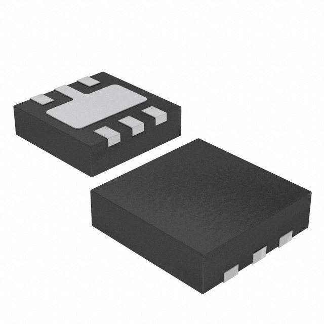
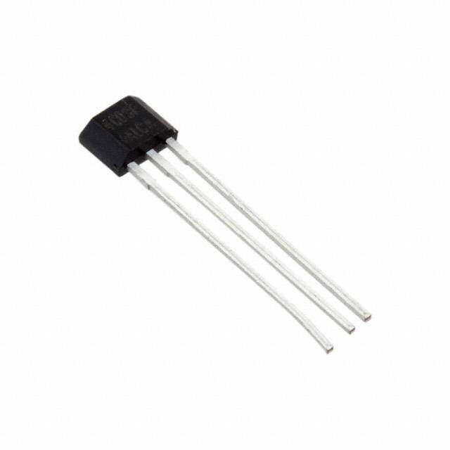
| 产品图片 |
|
| rohs | 符合RoHS无铅 / 符合限制有害物质指令(RoHS)规范要求 |
| 产品系列 | 电源管理 IC,低压差稳压器,Microchip Technology MCP1725-1202E/SN- |
| 数据手册 | http://www.microchip.com/mymicrochip/filehandler.aspx?ddocname=en520352 |
| 产品型号 | MCP1725-1202E/SN |
| PCN组件/产地 | http://www.microchip.com/mymicrochip/NotificationDetails.aspx?id=5774&print=view |
| PCN设计/规格 | http://www.microchip.com/mymicrochip/NotificationDetails.aspx?id=5576&print=viewhttp://www.microchip.com/mymicrochip/NotificationDetails.aspx?id=5704&print=view |
| PSRR/纹波抑制—典型值 | 60 dB |
| 产品培训模块 | http://www.digikey.cn/PTM/IndividualPTM.page?site=cn&lang=zhs&ptm=4201 |
| 产品目录页面 | |
| 产品种类 | 低压差稳压器 |
| 供应商器件封装 | 8-SOIC N |
| 其它名称 | MCP17251202ESN |
| 包装 | 管件 |
| 参考电压 | 0.41 V |
| 商标 | Microchip Technology |
| 回动电压—最大值 | 350 mV |
| 安装类型 | 表面贴装 |
| 安装风格 | SMD/SMT |
| 封装 | Tube |
| 封装/外壳 | 8-SOIC(0.154",3.90mm 宽) |
| 封装/箱体 | SOIC-8 Narrow |
| 工作温度 | -40°C ~ 125°C |
| 工厂包装数量 | 100 |
| 最大工作温度 | + 125 C |
| 最大输入电压 | 6 V |
| 最小工作温度 | - 40 C |
| 最小输入电压 | 2.3 V |
| 标准包装 | 100 |
| 电压-跌落(典型值) | 0.21V @ 500mA |
| 电压-输入 | 2.3 V ~ 6 V |
| 电压-输出 | 1.2V |
| 电压调节准确度 | 0.5 % |
| 电流-输出 | 500mA |
| 电流-限制(最小值) | - |
| 稳压器拓扑 | 正,固定式 |
| 稳压器数 | 1 |
| 线路调整率 | 0.05 %/V |
| 负载调节 | 0.5 % |
| 输入偏压电流—最大 | 0.12 mA |
| 输出电压 | 1.2 V |
| 输出电压容差 | 2 % |
| 输出电流 | 500 mA |
| 输出端数量 | 1 Output |
| 输出类型 | Fixed |


- 商务部:美国ITC正式对集成电路等产品启动337调查
- 曝三星4nm工艺存在良率问题 高通将骁龙8 Gen1或转产台积电
- 太阳诱电将投资9.5亿元在常州建新厂生产MLCC 预计2023年完工
- 英特尔发布欧洲新工厂建设计划 深化IDM 2.0 战略
- 台积电先进制程称霸业界 有大客户加持明年业绩稳了
- 达到5530亿美元!SIA预计今年全球半导体销售额将创下新高
- 英特尔拟将自动驾驶子公司Mobileye上市 估值或超500亿美元
- 三星加码芯片和SET,合并消费电子和移动部门,撤换高东真等 CEO
- 三星电子宣布重大人事变动 还合并消费电子和移动部门
- 海关总署:前11个月进口集成电路产品价值2.52万亿元 增长14.8%


PDF Datasheet 数据手册内容提取
MCP1725 500 mA, Low Voltage, Low Quiescent Current LDO Regulator Features Description • 500mA Output Current Capability The MCP1725 is a 500mA Low Dropout (LDO) linear • Input Operating Voltage Range: 2.3V to 6.0V regulator that provides high current and low output voltages in a very small package. The MCP1725 • Adjustable Output Voltage Range: 0.8V to 5.0V comes in a fixed (or adjustable) output voltage version, • Standard Fixed Output Voltages: with an output voltage range of 0.8V to 5.0V. The - 0.8V, 1.2V, 1.8V, 2.5V, 3.0V, 3.3V, 5.0V 500mA output current capability, combined with the • Other Fixed Output Voltage Options Available low output voltage capability, make the MCP1725 a Upon Request good choice for new sub-1.8V output voltage LDO • Low Dropout Voltage: 210mV typical at 500mA applications that have high current demands. • Typical Output Voltage Tolerance: 0.5% The MCP1725 is stable using ceramic output • Stable with 1.0µF Ceramic Output Capacitor capacitors that inherently provide lower output noise and reduce the size and cost of the entire regulator • Fast response to Load Transients solution. Only 1µF of output capacitance is needed to • Low Supply Current: 120µA (typical) stabilize the LDO. • Low Shutdown Supply Current: 0.1µA (typical) Using CMOS construction, the quiescent current • Adjustable Delay on Power Good Output consumed by the MCP1725 is typically less than • Short Circuit Current Limiting and 120µA over the entire input voltage range, making it Overtemperature Protection attractive for portable computing applications that • 2x3 DFN-8 and SOIC-8 Package Options demand high output current. When shut down, the quiescent current is reduced to less than 0.1µA. Applications The scaled-down output voltage is internally monitored • High-Speed Driver Chipset Power and a power good (PWRGD) output is provided when the output is within 92% of regulation (typical). An • Networking Backplane Cards external capacitor can be used on the C pin to DELAY • Notebook Computers adjust the delay from 200µs to 300ms. • Network Interface Cards The overtemperature and short circuit current-limiting • Palmtop Computers provide additional protection for the LDO during system • Video Graphics Adapters fault conditions. • 2.5V to 1.XV Regulators Package Types Adjustable (SOIC-8) Fixed (SOIC-8) Adjustable (2x3 DFN) Fixed (2x3 DFN) VIN 1 8 VOUT VIN 1 8 VOUT VIN 1 8 VOUT VIN 1 8 VOUT VIN 2 7 ADJ VIN 2 7 Sense VIN 2 7 ADJ VIN 2 7 Sense SHDN 3 6 CDELAY SHDN 3 6 CDELAY GND 4 5 PWRGD GND 4 5 PWRGD SHDN 3 6 CDELAY SHDN 3 6 CDELAY GND 4 5 PWRGD GND 4 5 PWRGD Note: DFN tab is at ground potential. © 2007 Microchip Technology Inc. DS22026B-page 1
MCP1725 Typical Application MCP1725 Fixed Output Voltage VIN = 2.3V to 2.8V 1 V V 8 VOUT = 1.8V @ 500mA IN OUT 2 V Sense 7 C1 IN C2 4.7µF 1µF 3 SHDN C 6 DELAY R 1 4 GND PWRGD 5 100kΩ C On 3 1000pF Off PWRGD MCP1725 Adjustable Output Voltage VIN = 2.3V to 2.8V 1 V V 8 VOUT = 1.2V @ 500mA IN OUT R 1 2 VIN ADJ 7 40kΩ C1 C2 4.7µF 1µF 3 SHDN C 6 DELAY R 3 4 GND PWRGD 5 100kΩ On R C 2 Off 10300pF 20kΩ PWRGD DS22026B-page 2 © 2007 Microchip Technology Inc.
MCP1725 Functional Block Diagram - Adjustable Output PMOS V V IN OUT Undervoltage Lock Out (UVLO) I SNS Cf Rf SHDN ADJ + Driver w/limit EA and SHDN Overtemperature – Sensing SHDN V REF VIN SHDN Reference Soft-Start PWRGD Comp T DELAY GND 92% of V REF C DELAY © 2007 Microchip Technology Inc. DS22026B-page 3
MCP1725 Functional Block Diagram - Fixed Output PMOS VIN VOUT Undervoltage Lock Out (UVLO) I SNS Cf Rf SHDN Sense + Driver w/limit EA and SHDN Overtemperature – Sensing SHDN V REF VIN SHDN Reference Soft-Start PWRGD Comp T DELAY GND 92% of V REF C DELAY DS22026B-page 4 © 2007 Microchip Technology Inc.
MCP1725 1.0 ELECTRICAL † Notice: Stresses above those listed under “Maximum CHARACTERISTICS Ratings” may cause permanent damage to the device. This is a stress rating only and functional operation of the device at those or any other conditions above those Absolute Maximum Ratings † indicated in the operational listings of this specification is not implied. Exposure to maximum rating conditions V .........................................................................6.5V IN for extended periods may affect device reliability. Maximum Voltage on Any Pin ........................................(GND – 0.3V) to (V + 0.3)V IN Maximum Power Dissipation.............Internally-Limited (Note6) Output Short Circuit Duration.....................Continuous Storage temperature..........................-65°C to +150°C Maximum Junction Temperature, T ................+150°C J ESD protection on all pins (HBM/MM).. ≥ 2kV; ≥ 200V AC/DC CHARACTERISTICS Electrical Specifications: Unless otherwise noted, V = V + V (Note1), V = 1.8V for Adjustable Output, IN OUT(MAX) DROPOUT(MAX) R I = 1mA, C = C = 4.7µF (X7R Ceramic), T = +25°C. OUT IN OUT A Boldface type applies for junction temperatures, T (Note7) of -40°C to +125°C J Parameters Sym Min Typ Max Units Conditions Input Operating Voltage V 2.3 6.0 V Note1 IN Input Quiescent Current I — 120 220 µA I = 0mA, V = Note1, q L IN V = 0.8V to 5.0V OUT Input Quiescent Current for I — 0.1 3 µA SHDN = GND SHDN SHDN Mode Maximum Output Current I 500 — — mA V = 2.3V to 6.0V OUT IN V = 0.8V to 5.0V, Note1 R Line Regulation ΔV / — ±0.05 ±0.16 %/V (Note1) ≤ V ≤ 6V OUT IN (V x ΔV ) OUT IN Load Regulation ΔV /V -1.0 ±0.5 1.0 % I = 1mA to 500mA, OUT OUT OUT (Note4) Output Short Circuit Current I — 1.2 — A R <0.1Ω, Peak Current OUT_SC LOAD Adjust Pin Characteristics (Adjustable Output Only) Adjust Pin Reference Voltage V 0.402 0.410 0.418 V V = 2.3V to V =6.0V, ADJ IN IN I = 1mA OUT Adjust Pin Leakage Current I -10 ±0.01 +10 nA V = 6.0V, V =0Vto6V ADJ IN ADJ Adjust Temperature Coefficient TCV — 40 — ppm/°C Note3 OUT Fixed-Output Characteristics (Fixed Output Only) Voltage Regulation V V - 2.5% V ±0.5% V + 2.5% V Note2 OUT R R R Note 1: The minimum V must meet two conditions: V ≥ 2.3V and V ≥ V + V IN IN IN OUT(MAX) DROPOUT(MAX). 2: V is the nominal regulator output voltage for the fixed cases. V = 1.2V, 1.8V, etc. V is the desired set point output R R R voltage for the adjustable cases. V = V ((R /R )+1). Figure4-1. R ADJ* 1 2 3: TCV = (V – V ) *106 / (V * ΔTemperature). V is the highest voltage measured over the OUT OUT-HIGH OUT-LOW R OUT-HIGH temperature range. V is the lowest voltage measured over the temperature range. OUT-LOW 4: Load regulation is measured at a constant junction temperature using low duty-cycle pulse testing. Load regulation is tested over a load range from 1mA to the maximum specified output current. 5: Dropout voltage is defined as the input-to-output voltage differential at which the output voltage drops 2% below its nominal value that was measured with an input voltage of V = V + V . OUT R DROPOUT(MAX) 6: The maximum allowable power dissipation is a function of ambient temperature, the maximum allowable junction temperature and the thermal resistance from junction to air. (i.e., T , T , θ ). Exceeding the maximum allowable power A J JA dissipation will cause the device operating junction temperature to exceed the maximum +150°C rating. Sustained junction temperatures above +150°C can impact device reliability. 7: The junction temperature is approximated by soaking the device under test at an ambient temperature equal to the desired junction temperature. The test time is small enough such that the rise in the junction temperature over the ambient temperature is not significant. © 2007 Microchip Technology Inc. DS22026B-page 5
MCP1725 AC/DC CHARACTERISTICS (CONTINUED) Electrical Specifications: Unless otherwise noted, V = V + V (Note1), V = 1.8V for Adjustable Output, IN OUT(MAX) DROPOUT(MAX) R I = 1mA, C = C = 4.7µF (X7R Ceramic), T = +25°C. OUT IN OUT A Boldface type applies for junction temperatures, T (Note7) of -40°C to +125°C J Parameters Sym Min Typ Max Units Conditions Dropout Characteristics Dropout Voltage V -V — 210 350 mV I = 500 mA, (Note5) IN OUT OUT V =2.3V IN(MIN) Power Good Characteristics PWRGD Input Voltage Operat- V 1.0 — 6.0 V T = +25°C PWRGD_VIN A ing Range 1.2 — 6.0 T = -40°C to +125°C A For V < 2.3V, I =100µA IN SINK PWRGD Threshold Voltage V — — — %V Falling Edge PWRGD_TH OUT (Referenced to V ) OUT 89 92 95 V < 2.5V Fixed, V = OUT OUT Adj. 90 92 94 V >= 2.5V Fixed OUT PWRGD Threshold Hysteresis V 1.0 2.0 3.0 %V PWRGD_HYS OUT PWRGD Output Voltage Low V — 0.2 0.4 V I = 1.2mA, PWRGD_L PWRGDSINK ADJ = 0V, SENSE = 0V PWRGD Leakage P _ — 1 — nA V = V = 6.0V WRGD LK PWRGD IN PWRGD Time Delay T Rising Edge PG R = 10kΩ PULLUP I CDELAY = 140nA (Typ) — 200 — µs C =OPEN DELAY 10 30 55 ms C =0.01µF DELAY — 300 — ms C =0.1µF DELAY Detect Threshold to PWRGD T — 200 — µs V or V = VDET-PWRGD ADJ SENSE Active Time Delay V + 20mV to PWRGD_TH V - 20mV PWRGD_TH Shutdown Input Logic High Input V 45 — — %V V = 2.3V to 6.0V SHDN-HIGH IN IN Logic Low Input V — — 15 %V V = 2.3V to 6.0V SHDN-LOW IN IN SHDN Input Leakage Current SHDN -0.1 ±0.001 +0.1 µA V =6V, SHDN =V , ILK IN IN SHDN = GND Note 1: The minimum V must meet two conditions: V ≥ 2.3V and V ≥ V + V IN IN IN OUT(MAX) DROPOUT(MAX). 2: V is the nominal regulator output voltage for the fixed cases. V = 1.2V, 1.8V, etc. V is the desired set point output R R R voltage for the adjustable cases. V = V ((R /R )+1). Figure4-1. R ADJ* 1 2 3: TCV = (V – V ) *106 / (V * ΔTemperature). V is the highest voltage measured over the OUT OUT-HIGH OUT-LOW R OUT-HIGH temperature range. V is the lowest voltage measured over the temperature range. OUT-LOW 4: Load regulation is measured at a constant junction temperature using low duty-cycle pulse testing. Load regulation is tested over a load range from 1mA to the maximum specified output current. 5: Dropout voltage is defined as the input-to-output voltage differential at which the output voltage drops 2% below its nominal value that was measured with an input voltage of V = V + V . OUT R DROPOUT(MAX) 6: The maximum allowable power dissipation is a function of ambient temperature, the maximum allowable junction temperature and the thermal resistance from junction to air. (i.e., T , T , θ ). Exceeding the maximum allowable power A J JA dissipation will cause the device operating junction temperature to exceed the maximum +150°C rating. Sustained junction temperatures above +150°C can impact device reliability. 7: The junction temperature is approximated by soaking the device under test at an ambient temperature equal to the desired junction temperature. The test time is small enough such that the rise in the junction temperature over the ambient temperature is not significant. DS22026B-page 6 © 2007 Microchip Technology Inc.
MCP1725 AC/DC CHARACTERISTICS (CONTINUED) Electrical Specifications: Unless otherwise noted, V = V + V (Note1), V = 1.8V for Adjustable Output, IN OUT(MAX) DROPOUT(MAX) R I = 1mA, C = C = 4.7µF (X7R Ceramic), T = +25°C. OUT IN OUT A Boldface type applies for junction temperatures, T (Note7) of -40°C to +125°C J Parameters Sym Min Typ Max Units Conditions AC Performance Output Delay From SHDN T — 100 — µs SHDN = GND to V OR IN V = GND to 95% V OUT R Output Noise e — 2.0 — µV/√Hz I = 200mA, f = 1kHz, N OUT C = 10µF (X7R Ceramic), OUT V = 2.5V OUT Power Supply Ripple Rejection PSRR — 60 — dB f = 100Hz, C = 10µF, OUT Ratio I = 10mA, OUT V = 30mV pk-pk, INAC C = 0µF IN Thermal Shutdown Temperature T — 150 — °C I = 100µA, V = 1.8V, SD OUT OUT V = 2.8V IN Thermal Shutdown Hysteresis ΔT — 10 — °C I = 100µA, V = 1.8V, SD OUT OUT V = 2.8V IN Note 1: The minimum V must meet two conditions: V ≥ 2.3V and V ≥ V + V IN IN IN OUT(MAX) DROPOUT(MAX). 2: V is the nominal regulator output voltage for the fixed cases. V = 1.2V, 1.8V, etc. V is the desired set point output R R R voltage for the adjustable cases. V = V ((R /R )+1). Figure4-1. R ADJ* 1 2 3: TCV = (V – V ) *106 / (V * ΔTemperature). V is the highest voltage measured over the OUT OUT-HIGH OUT-LOW R OUT-HIGH temperature range. V is the lowest voltage measured over the temperature range. OUT-LOW 4: Load regulation is measured at a constant junction temperature using low duty-cycle pulse testing. Load regulation is tested over a load range from 1mA to the maximum specified output current. 5: Dropout voltage is defined as the input-to-output voltage differential at which the output voltage drops 2% below its nominal value that was measured with an input voltage of V = V + V . OUT R DROPOUT(MAX) 6: The maximum allowable power dissipation is a function of ambient temperature, the maximum allowable junction temperature and the thermal resistance from junction to air. (i.e., T , T , θ ). Exceeding the maximum allowable power A J JA dissipation will cause the device operating junction temperature to exceed the maximum +150°C rating. Sustained junction temperatures above +150°C can impact device reliability. 7: The junction temperature is approximated by soaking the device under test at an ambient temperature equal to the desired junction temperature. The test time is small enough such that the rise in the junction temperature over the ambient temperature is not significant. TEMPERATURE SPECIFICATIONS Electrical Specifications: Unless otherwise indicated, all limits apply for V = 2.3V to 6.0V. IN Parameters Sym Min Typ Max Units Conditions Temperature Ranges Operating Junction Temperature Range T -40 — +125 °C Steady State J Maximum Junction Temperature T — — +150 °C Transient J Storage Temperature Range T -65 — +150 °C A Thermal Package Resistances Thermal Resistance, 8LD 2x3 DFN θ — 76 — °C/W 4-Layer JC51-7 JA θ — 26 — °C/W Standard Board with JC vias Thermal Resistance, 8LD SOIC θ — 163 — °C/W 4-Layer JC51-7 JA θ — 38.8 — °C/W Standard Board JC © 2007 Microchip Technology Inc. DS22026B-page 7
MCP1725 2.0 TYPICAL PERFORMANCE CURVES Note: The graphs and tables provided following this note are a statistical summary based on a limited number of samples and are provided for informational purposes only. The performance characteristics listed herein are not tested or guaranteed. In some graphs or tables, the data presented may be outside the specified operating range (e.g., outside specified power supply range) and therefore outside the warranted range. Note: Unless otherwise indicated, V = V + 0.5V or V = 2.3V (whichever is greater), I = 1mA, C = C = IN OUT IN OUT IN OUT 4.7µF Ceramic (X7R), SHDN = V , C = Open, Fixed Output Version, and T = +25°C. IN DELAY A Note: Junction Temperature (T ) is approximated by soaking the device under test to an ambient temperature equal to J the desired junction temperature. The test time is small enough such that the rise in Junction Temperature over the Ambient temperature is not significant. 150 0.12 IOUT = 0 mA VIN = 2.3V to 6.0V ent (µA) 113400 +90°C+130°C n (%/V) 00..0180 IOUT = 1 mA IOUT = 500 mA nt Curr 111200 gulatio 0.06 IOUT = 50 mA Quiesce 10900 0°C +25°C Line Re 00..0024 IOUT = 100 mA IOUT = 250 mA -45°C 80 0.00 2 3 4 5 6 -45 -20 5 30 55 80 105 130 Input Voltage (V) Temperature (°C) FIGURE 2-1: Quiescent Current vs. Input FIGURE 2-4: Line Regulation vs. Voltage (1.8V Adjustable). Temperature (1.8V Adjustable). 210 0.20 200 VOUT = 1.2V Adj 0.18 VOUT = 3.3V A) 190 %) 0.16 Current (µ 111678000 gulation ( 000...111024 VOUT = 1.8V VOUT = 0.8V Ground 111345000 VIN = 5.0V VIN = 3.3V VIN = 2.5V Load Re 0000....00002468 VOUT = 5V IOUT = 1.0 mA to 500 mA 120 0.00 0 100 200 300 400 500 -45 -20 5 30 55 80 105 130 Load Current (mA) Temperature (°C) FIGURE 2-2: Ground Current vs. Load FIGURE 2-5: Load Regulation vs. Current (1.2V Adjustable). Temperature (Adjustable Version). 150 0.412 IOUT = 0 mA IOUT = 1 mA A) 140 V) nt Current (µ 111123000 VIN = 5.0V VIN = 6.0V Pin Voltage ( 00..441101 VIN = 6.0V VIN = 5.0V Quiesce 10900 VIN = 2.3V VIN = 3.3V Adjust 0.409 VIN = 2.3V, 3.0V, 4.0V 80 0.408 -45 -20 5 30 55 80 105 130 -45 -20 5 30 55 80 105 130 Temperature (°C) Temperature (°C) FIGURE 2-3: Quiescent Current vs. FIGURE 2-6: Adjust Pin Voltage vs. Junction Temperature (1.8V Adjustable). Temperature. DS22026B-page 8 © 2007 Microchip Technology Inc.
MCP1725 Note: Unless otherwise indicated, V = V + 0.5V or V = 2.3V (whichever is greater), I = 1mA, IN OUT IN OUT C = C = 4.7µF Ceramic (X7R), SHDN = V , C = Open, Fixed Output Version, and T = +25°C. IN OUT IN DELAY A 0.25 150 IOUT = 0 mA VOUT = 5.0V A) 140 e (V) 0.20 nt (µ 130 +130°C Voltag 0.15 VOUT = 2.5V Curre 120 ut 0.10 nt 110 Dropo 0.05 Quiesce 10900 0°C +25°C +90°C -45°C 0.00 80 0 100 200 300 400 500 2 3 4 5 6 Load Current (mA) Input Voltage (V) FIGURE 2-7: Dropout Voltage vs. Load FIGURE 2-10: Quiescent Current vs. Input Current (Adjustable Version). Voltage (0.8V Fixed). 0.28 150 IOUT = 500 mA IOUT = 0 mA 0.26 A) 140 V) µ Voltage ( 00..2224 VOUT = 5.0V VOUT = 3.3V Current ( 112300 ut nt Dropo 00..1280 VOUT = 2.5V uiesce 110100 +135°C Q -45°C 0°C +25°C +90°C 0.16 90 -45 -20 5 30 55 80 105 130 3 3.5 4 4.5 5 5.5 6 Temperature (°C) Input Voltage (V) FIGURE 2-8: Dropout Voltage vs. FIGURE 2-11: Quiescent Current vs. Input Temperature (Adjustable Version). Voltage (2.5V Fixed). 35 210 Delay (ms) 33331234 VIN = 2.3V CIODUETL =AY 0 = m 0A.01 µF ent (µA) 117900 Time 2390 VIN = 5.0V d Curr 150 VOUT = 5.0V Good 2278 VIN = 3.0V Groun 130 VOUT = 2.5V er 26 ow 25 110 P -45 -20 5 30 55 80 105 130 0 100 200 300 400 500 Temperature (°C) Load Current (mA) FIGURE 2-9: Power Good (PWRGD) FIGURE 2-12: Ground Current vs. Load Time Delay vs. Temperature (Adjustable Current. Version). © 2007 Microchip Technology Inc. DS22026B-page 9
MCP1725 Note: Unless otherwise indicated, V = V + 0.5V or V = 2.3V (whichever is greater), I = 1mA, IN OUT IN OUT C = C = 4.7µF Ceramic (X7R), SHDN = V , C = Open, Fixed Output Version, and T = +25°C. IN OUT IN DELAY A 140 0.050 ent (µA) 112300 IOUT = 0 mA n (%/V) 000...000344505 IOUT = 1 mA VIN = 3V.0OVUT to= 26..50VV cent Curr 110100 VOUT = 2.5V Regulatio 00..002350 IOUT = 50 mA Quies 90 VOUT = 0.8V Line 00..001250 IOUT = 250 mA IOUT = 500 mA IOUT = 100 mA 80 0.010 -45 -20 5 30 55 80 105 130 -45 -20 5 30 55 80 105 130 Junction Temperature (°C) Temperature (°C) FIGURE 2-13: Quiescent Current vs. FIGURE 2-16: Line Regulation vs. Junction Temperature. Temperature (2.5V Fixed). 1.0 0.20 0.9 VOUT = 0.8V 0.18 IOUT = 1.0 mA to 500 mA 0.8 %) 0.16 VOUT = 0.8V 0.7 n ( 0.14 µA) 0.6 atio 0.12 VOUT = 1.2V I (SHDN 0000....2345 VIN = 6.0VVIN = 3.3V VIN = 2.3V oad Regul 000...001680 L 0.1 0.04 0.0 0.02 -45 -20 5 30 55 80 105 130 -45 -20 5 30 55 80 105 130 Temperature (°C) Temperature (°C) FIGURE 2-14: I vs. Temperature. FIGURE 2-17: Load Regulation vs. SHDN Temperature (V < 2.5V Fixed). OUT 0.10 0.00 gulation (%/V) 000000......000000456789 IOUT = 1IO0U0T m= A1 mA VIN = I2OV.U3OTV U=T t 5o=0 06 m..80AVV egulation (%) ----0000....21100505 VVOOUUTT == 52..05VV IOUT = 1.0 mA to 500 mA e Re 0.03 IOUT = 250 mA ad R -0.25 n 0.02 o Li 0.01 IOUT = 500 mA L -0.30 0.00 -0.35 -45 -20 5 30 55 80 105 130 -45 -20 5 30 55 80 105 130 Temperature (°C) Temperature (°C) FIGURE 2-15: Line Regulation vs. FIGURE 2-18: Load Regulation vs. Temperature (0.8V Fixed). Temperature (V ≥ 2.5V Fixed). OUT DS22026B-page 10 © 2007 Microchip Technology Inc.
MCP1725 Note: Unless otherwise indicated, V = V + 0.5V or V = 2.3V (whichever is greater), I = 1mA, IN OUT IN OUT C = C = 4.7µF Ceramic (X7R), SHDN = V , C = Open, Fixed Output Version, and T = +25°C. IN OUT IN DELAY A 0.25 opout Voltage (V) 000...112050 VOVUTO U=T 5=. 02V.5V oise (μV/Hz)(cid:165) 01.110 VVIONU =T =2 .03.V8V VVIONU =T =3 .23.V5V ILOACDC O=INU T2= 0= 10 10 m μμAFF Dr 0.05 N 0.01 0.00 0.001 0 100 200 300 400 500 0.01 0.1 1 10 100 1000 Load Current (mA) Frequency (kHz) FIGURE 2-19: Dropout Voltage vs. Load FIGURE 2-22: Output Noise Voltage Current. Density vs. Frequency. 0.28 0.26 ILOAD = 500 mA 0 -10 V) 0.24 ge ( 0.22 VOUT = 5.0V -20 olta 0.20 dB)-30 ut V 0.18 VOUT = 2.5V RR (-40 VR=1.2V Adj po 0.16 PS-50 COUT=4.7 μF ceramic X7R Dro 00..1124 -60 VCIINN==20. 5μVF -70 IOUT=10 mA 0.10 -80 -45 -20 5 30 55 80 105 130 0.01 0.1 1 10 100 1000 Temperature (°C) Frequency (kHz) FIGURE 2-20: Dropout Voltage vs. FIGURE 2-23: Power Supply Ripple Temperature. Rejection (PSRR) vs. Frequency (V = 1.2V OUT Adj.). 1.20 A) 1.10 IPEAK 0 ent ( 1.00 VOUT = 2.5V Fixed --2100 Curr 0.90 CIN= 3000 µF B)-30 uit 0.80 R (d-40 hort Circ 00..6700 ISTEADY STATE PSR--6500 VCVCRIOINN=U==T120=.. 225μV2VF AμFd jceramic X7R S -70 IOUT=10 mA 0.50 -80 3.0 3.5 4.0 4.5 5.0 5.5 6.0 0.01 0.1 1 10 100 1000 Input Voltage (V) Frequency (kHz) FIGURE 2-21: Short Circuit Current vs. FIGURE 2-24: Power Supply Ripple Input Voltage. Rejection (PSRR) vs. Frequency (V = 1.2V OUT Adj.). © 2007 Microchip Technology Inc. DS22026B-page 11
MCP1725 Note: Unless otherwise indicated, V = V + 0.5V or V = 2.3V (whichever is greater), I = 1mA, IN OUT IN OUT C = C = 4.7µF Ceramic (X7R), SHDN = V , C = Open, Fixed Output Version, and T = +25°C. IN OUT IN DELAY A 0 -10 -20 B)-30 d R (-40 R VR=2.5V Fixed PS-50 COUT=4.7 μF ceramic X7R -60 VIN=3.3V CIN=0 μF -70 IOUT=10 mA -80 0.01 0.1 1 10 100 1000 Frequency (KHz) FIGURE 2-25: Power Supply Ripple FIGURE 2-28: 2.5V (Adj.) Startup from Rejection (PSRR) vs. Frequency (V = 2.5V Shutdown. OUT Fixed). 0 -10 -20 B)-30 d R (-40 R VR=2.5V Fixed PS-50 COUT=22 μF ceramic X7R -60 VIN=3.3V CIN=0 μF -70 IOUT=10 mA -80 0.01 0.1 1 10 100 1000 Frequency (KHz) FIGURE 2-26: Power Supply Ripple FIGURE 2-29: Power Good (PWRGD) Rejection (PSRR) vs. Frequency (V = 2.5V Timing with Cdelay of 1000pF (2.5V Fixed). OUT Fixed). FIGURE 2-27: 2.5V (Adj.) Startup from V . FIGURE 2-30: Power Good (PWRGD) IN Timing with C of 0.01µF (2.5V Fixed). DELAY DS22026B-page 12 © 2007 Microchip Technology Inc.
MCP1725 Note: Unless otherwise indicated, V = V + 0.5V or V = 2.3V (whichever is greater), I = 1mA, IN OUT IN OUT C = C = 4.7µF Ceramic (X7R), SHDN = V , C = Open, Fixed Output Version, and T = +25°C. IN OUT IN DELAY A FIGURE 2-31: Dynamic Line Response FIGURE 2-33: Dynamic Load Response (5.0V Fixed). (2.5V Fixed, 1mA to 500mA). FIGURE 2-32: Dynamic Line Response FIGURE 2-34: Dynamic Load Response (2.5V Fixed). (2.5V Fixed, 10mA to 500mA). © 2007 Microchip Technology Inc. DS22026B-page 13
MCP1725 3.0 PIN DESCRIPTION The descriptions of the pins are listed in Table3-1. TABLE 3-1: PIN FUNCTION TABLE Adjustable Fixed Output Name Description Output 1 1 V Input Voltage Supply IN 2 2 V Input Voltage Supply IN 3 3 SHDN Shutdown Control Input (active-low) 4 4 GND Ground 5 5 PWRGD Power Good Output (open-drain) 6 6 C Power Good Delay Set-Point Input DELAY — 7 ADJ Voltage Sense Input (adjustable version) 7 — Sense Voltage Sense Input (fixed voltage version) 8 8 V Regulated Output Voltage OUT Exposed Pad Exposed Pad EP Exposed Pad of the DFN Package (ground potential) 3.1 Input Voltage Supply (V ) 3.4 Power Good Output (PWRGD) IN Connect the unregulated or regulated input voltage The PWRGD output is an open-drain output used to source to V . If the input voltage source is located indicate when the LDO output voltage is within 92% IN several inches away from the LDO, or the input source (typically) of its nominal regulation value. The PWRGD is a battery, it is recommended that an input capacitor threshold has a typical hysteresis value of 2%. The be used. A typical input capacitance value of 1µF to PWRGD output is typically delayed by 200µs (typical, 10µF should be sufficient for most applications. no capacitance on C pin) from the time the LDO DELAY output is within 92% + 3% (max hysteresis) of the 3.2 Shutdown Control Input (SHDN) regulated output value on power-up. This delay time is controlled by the C pin. DELAY The SHDN input is used to turn the LDO output voltage on and off. When the SHDN input is at a logic-high 3.5 Power Good Delay Set-Point Input level, the LDO output voltage is enabled. When the (C ) SHDN input is pulled to a logic-low level, the LDO DELAY output voltage is disabled. When the SHDN input is The C input sets the power-up delay time for the DELAY pulled low, the PWRGD output also goes low and the PWRGD output. By connecting an external capacitor LDO enters a low quiescent current shutdown state from the C pin to ground, the typical delay times DELAY where the typical quiescent current is 0.1µA. for the PWRGD output can be adjusted from 200µs (no capacitance) to 300ms (0.1µF capacitor). This allows 3.3 Ground (GND) for the optimal setting of the system reset time. Connect the GND pin of the LDO to a quiet circuit ground. This will help the LDO power supply rejection ratio and noise performance. The ground pin of the LDO only conducts the quiescent current of the LDO (typically 120µA), so a heavy trace is not required. For applications that have switching or noisy inputs, tie the GND pin to the return of the output capacitor. Ground planes help lower inductance and voltage spikes caused by fast transient load currents and are recommended for applications that are subjected to fast load transients. DS22026B-page 14 © 2007 Microchip Technology Inc.
MCP1725 3.6 Output Voltage Sense/Adjust 3.7 Regulated Output Voltage (V ) OUT Input (ADJ/Sense) The V pin(s) is the regulated output voltage of the OUT LDO. A minimum output capacitance of 1.0µF is 3.6.1 ADJ required for LDO stability. The MCP1725 is stable with For adjustable applications, the output voltage is ceramic, tantalum and aluminum-electrolytic connected to the ADJ input through a resistor divider capacitors. See Section4.3 “Output Capacitor” for that sets the output voltage regulation value. This output capacitor selection guidance. provides the user the capability to set the output voltage to any value they desire within the 0.8V to 5.0V 3.8 Exposed Pad (EP) range of the device. The 2x3 DFN package has an exposed pad on the 3.6.2 Sense bottom of the package. This pad should be soldered to the Printed Circuit Board (PCB) to aid in the removal of For fixed output voltage versions of the device, the heat from the package during operation. The exposed SENSE input is used to provide output voltage pad is at the ground potential of the LDO. feedback to the internal circuitry of the MCP1725. The SENSE pin typically improves load regulation by allowing the device to compensate for voltage drops due to packaging and circuit board layout. © 2007 Microchip Technology Inc. DS22026B-page 15
MCP1725 4.0 DEVICE OVERVIEW EQUATION 4-2: V –V The MCP1725 is a high output current, Low Dropout R = R ⎛----O----U----T------------A----D---J-⎞ 1 2⎝ V ⎠ (LDO) voltage regulator with an adjustable delay ADJ Where: power-good output and shutdown control input. The low dropout voltage of 210mV typical at 0.5A of current V = LDO Output Voltage OUT makes it ideal for battery-powered applications. Unlike V = ADJ Pin Voltage ADJ other high output current LDOs, the MCP1725 only (typically 0.41V) draws a maximum of 220µA of quiescent current. 4.1 LDO Output Voltage 4.2 Output Current and Current Limiting The MCP1725 LDO is available with either a fixed output voltage or an adjustable output voltage. The The MCP1725 LDO is tested and ensured to supply a output voltage range is 0.8V to 5.0V for both versions. minimum of 0.5A of output current. The MCP1725 has no minimum output load, so the output load current can 4.1.1 ADJUST INPUT go to 0mA and the LDO will continue to regulate the The adjustable version of the MCP1725 uses the ADJ output voltage to within tolerance. pin (pin 7) to get the output voltage feedback for output The MCP1725 also incorporates an output current limit. voltage regulation. This allows the user to set the If the output voltage falls below 0.7V due to an overload output voltage of the device with two external resistors. condition (usually represents a shorted load condition), The nominal voltage for ADJ is 0.41V. the output current is limited to 1.2A (typical). If the over- Figure4-1 shows the adjustable version of the load condition is a soft overload, the MCP1725 will MCP1725. Resistors R and R form the resistor supply higher load currents of up to 1A. The MCP1725 1 2 divider network necessary to set the output voltage. should not be operated in this condition continuously as With this configuration, the equation for setting V is: it may result in failure of the device. However, this does OUT allow for device usage in applications that have higher EQUATION 4-1: pulsed load currents having an average output current value of 0.5A or less. R +R VOUT = VADJ⎝⎛----1---R----------2-⎠⎞ Output overload conditions may also result in an over- Where: 2 temperature shutdown of the device. If the junction temperature rises above 150°C, the LDO will shut VOUT = LDO Output Voltage down the output voltage. See Section4.9 “Overtem- V = ADJ Pin Voltage perature Protection” for more information on ADJ (typically 0.41V) overtemperature shutdown. 4.3 Output Capacitor MCP1725-ADJ The MCP1725 requires a minimum output capacitance VIN 1 VIN VOUT 8 VOUT of 1µF for output voltage stability. Ceramic capacitors 4C.71µF 2 VIN ADJ 7 R1 C2 aenrev irroencmomenmtaeln rdoebdu sbtneecsasu qseu aolitfi etsh.e ir size, cost and 3 SHDN CDELAY 6 1µF 4 GND PWRGD 5 Aluminum-electrolytic and tantalum capacitors can be On used on the LDO output as well. The Equivalent Series Off 1000pCF3 R2 Resistance (ESR) of the electrolytic output capacitor must be no greater than 1 ohm. The output capacitor should be located as close to the LDO output as is FIGURE 4-1: Typical Adjustable Output practical. Ceramic materials X7R and X5R have low Voltage Application Circuit. temperature coefficients and are well within the acceptable ESR range required. A typical 1µF X7R The allowable resistance value range for resistor R is 2 0805 capacitor has an ESR of 50 milli-ohms. from 10kΩ to 200kΩ. Solving the equation for R 1 Larger LDO output capacitors can be used with the yields the following equation: MCP1725 to improve dynamic performance and power supply ripple rejection performance. A maximum of 22µF is recommended. Aluminum-electrolytic capacitors are not recommended for low-temperature applications of < -25°C. DS22026B-page 16 © 2007 Microchip Technology Inc.
MCP1725 4.4 Input Capacitor The power good output is an open-drain output that can be pulled up to any voltage that is equal to or less than Low input source impedance is necessary for the LDO the LDO input voltage. This output is capable of sinking output to operate properly. When operating from 1.2mA (V < 0.4V maximum). PWRGD batteries, or in applications with long lead length (> 10 inches) between the input source and the LDO, some input capacitance is recommended. A minimum of 1.0µF to 4.7µF is recommended for most VPWRGD_TH applications. For applications that have output step load VOUT requirements, the input capacitance of the LDO is very TPG important. The input capacitance provides the LDO with a good local low-impedance source to pull the VOH transient currents from in order to respond quickly to TVDET_PWRGD the output load step. For good step response performance, the input capacitor should be of PWRGD equivalent (or higher) value than the output capacitor. The capacitor should be placed as close to the input of VOL the LDO as is practical. Larger input capacitors will also help reduce any high-frequency noise on the input and output of the LDO and reduce the effects of any FIGURE 4-2: Power Good Timing. inductance that exists between the input source voltage and the input capacitance of the LDO. 4.5 Power Good Output (PWRGD) VIN TOR The PWRGD output is used to indicate when the output voltage of the LDO is within 92% (typical value, see 70µs 30µs Section1.0 “Electrical Characteristics” for Minimum and Maximum specifications) of its nominal regulation value. SHDN TPG As the output voltage of the LDO rises, the PWRGD output will be held low until the output voltage has exceeded the power good threshold plus the hysteresis value. Once this threshold has been exceeded, the VOUT power good time delay is started (shown as T in PG Section1.0 “Electrical Characteristics”). The power good time delay is adjustable via the C pin of the DELAY LDO (see Section4.6 “C Input”). By placing a DELAY PWRGD capacitor from the C pin to ground, the power DELAY good time delay can be adjusted from 200µs (no capacitance) to 300ms (0.1µF capacitor). After the time delay period, the PWRGD output will go high, indi- FIGURE 4-3: Power Good Timing from cating that the output voltage is stable and within Shutdown. regulation limits. If the output voltage of the LDO falls below the power good threshold, the power good output will transition low. The power good circuitry has a 170µs delay when detecting a falling output voltage, which helps to increase noise immunity of the power good output and avoid false triggering of the power good output during fast output transients. See Figure4-2 for power good timing characteristics. When the LDO is put into Shutdown mode using the SHDN input, the power good output is pulled low immediately, indicating that the output voltage will be out of regulation. The timing diagram for the power good output when using the shutdown input is shown in Figure4-3. © 2007 Microchip Technology Inc. DS22026B-page 17
MCP1725 4.6 C Input 4.7 Shutdown Input (SHDN) DELAY The C input is used to provide the power-up delay The SHDN input is an active-low input signal that turns DELAY timing for the power good output, as discussed in the the LDO on and off. The SHDN threshold is a previous section. By adding a capacitor from the percentage of the input voltage. The typical value of C pin to ground, the PWRGD power-up time this shutdown threshold is 30% of V , with minimum DELAY IN delay can be adjusted from 200µs (no capacitance on and maximum limits over the entire operating C ) to 300ms (0.1µF of capacitance on C ). temperature range of 45% and 15%, respectively. DELAY DELAY See Section1.0 “Electrical Characteristics” for The SHDN input will ignore low-going pulses (pulses C timing tolerances. DELAY meant to shut down the LDO) that are up to 400ns in Once the power good threshold (rising) has been pulse width. If the shutdown input is pulled low for more reached, the C pin charges the external capacitor than 400ns, the LDO will enter Shutdown mode. This DELAY to V . The charging current is 140nA (typical). The small bit of filtering helps to reject any system noise IN PWRGD output will transition high when the C pin spikes on the shutdown input signal. DELAY voltage has charged to 0.42V. If the output falls below On the rising edge of the SHDN input, the shutdown the power good threshold limit during the charging time circuitry has a 30µs delay before allowing the LDO between 0.0V and 0.42V on the C pin, the DELAY output to turn on. This delay helps to reject any false C pin voltage will be pulled to ground, thus reset- DELAY turn-on signals or noise on the SHDN input signal. After ting the timer. The C pin will be held low until the DELAY the 30µs delay, the LDO output enters its soft-start output voltage of the LDO has once again risen above period as it rises from 0V to its final regulation value. If the power good rising threshold. A timing diagram the SHDN input signal is pulled low during the 30µs showing C , PWRGD and V is shown in DELAY OUT delay period, the timer will be reset and the delay time Figure4-4. will start over again on the next rising edge of the SHDN input. The total time from the SHDN input going high (turn-on) to the LDO output being in regulation is typically 100µs. See Figure4-5 for a timing diagram of VOUT VPWRGD_TH the SHDN input. VIN (typ) TOR TPG CDELAY 400ns (typ) 70µs 30µs 0V CDELAY Threshold (0.42V) SHDN PWRGD VOUT FIGURE 4-4: C and PWRGD Timing DELAY Diagram. FIGURE 4-5: Shutdown Input Timing Diagram. DS22026B-page 18 © 2007 Microchip Technology Inc.
MCP1725 4.8 Dropout Voltage and 4.9 Overtemperature Protection Undervoltage Lockout The MCP1725 LDO has temperature-sensing circuitry Dropout voltage is defined as the input-to-output to prevent the junction temperature from exceeding voltage differential at which the output voltage drops approximately 150°C. If the LDO junction temperature 2% below the nominal value that was measured with a does reach 150°C, the LDO output will be turned off V + 0.6V differential applied. The MCP1725 LDO has until the junction temperature cools to approximately R a very low dropout voltage specification of 210mV 140°C, at which point the LDO output will automatically (typical) at 0.5A of output current. See Section1.0 resume normal operation. If the internal power “Electrical Characteristics” for maximum dropout dissipation continues to be excessive, the device will voltage specifications. again shut off. The junction temperature of the die is a function of power dissipation, ambient temperature and The MCP1725 LDO operates across an input voltage package thermal resistance. See Section5.0 “Appli- range of 2.3V to 6.0V and incorporates input Undervolt- cation Circuits/Issues” for more information on LDO age Lockout (UVLO) circuitry that keeps the LDO power dissipation and junction temperature. output voltage off until the input voltage reaches a minimum of 2.18V (typical) on the rising edge of the input voltage. As the input voltage falls, the LDO output will remain on until the input voltage level reaches 2.04V (typical). Since the MCP1725 LDO undervoltage lockout activates at 2.04V as the input voltage is falling, the dropout voltage specification does not apply for output voltages that are less than 1.9V. For high-current applications, voltage drops across the PCB traces must be taken into account. The trace resistances can cause significant voltage drops between the input voltage source and the LDO. For applications with input voltages near 2.3V, these PCB trace voltage drops can sometimes lower the input voltage enough to trigger a shutdown due to undervoltage lockout. © 2007 Microchip Technology Inc. DS22026B-page 19
MCP1725 5.0 APPLICATION CIRCUITS/ In addition to the LDO pass element power dissipation, ISSUES there is power dissipation within the MCP1725 as a result of quiescent or ground current. The power dissipation as a result of the ground current can be 5.1 Typical Application calculated using the following equation: The MCP1725 is used for applications that require high EQUATION 5-2: LDO output current and a power good output. P = V ×I I(GND) IN(MAX) VIN Where: MCP1725-2.5 VIN = 3.3V VOUT = 2.5V @ 0.5A P = Power dissipation due to the 1 VIN VOUT 8 I(GND quiescent current of the LDO 1C01µF 23 SVHINDNCSDeEnLAsYe 67 10kRΩ1 1C02µF VIN(MAX) = Maximum input voltage I = Current flowing in the V pin 4 GND PWRGD 5 VIN IN On with no LDO output current Off C3 (LDO quiescent current) 1000pF The total power dissipated within the MCP1725 is the sum of the power dissipated in the LDO pass device and the P(I ) term. Because of the CMOS PWRGD GND construction, the typical I for the MCP1725 is GND 120µA. Operating at 3.465V results in a power dissipa- FIGURE 5-1: Typical Application Circuit. tion of 0.42milli-Watts. For most applications, this is 5.1.1 APPLICATION CONDITIONS small compared to the LDO pass device power dissipation and can be neglected. Package Type = 2x3 DFN8 The maximum continuous operating junction Input Voltage Range = 3.3V ± 5% temperature specified for the MCP1725 is +125°C. To V maximum = 3.465V estimate the internal junction temperature of the IN MCP1725, the total internal power dissipation is V minimum = 3.135V IN multiplied by the thermal resistance from junction to V = 0.350V DROPOUT (max) ambient (Rθ ) of the device. The thermal resistance JA VOUT (typical) = 2.5V from junction to ambient for the 2x3 DFN package is I = 0.5A maximum estimated at 76°C/W. OUT P (typical) = 0.4W DISS EQUATION 5-3: Temperature Rise = 30.4°C T = P ×Rθ +T J(MAX) TOTAL JA AMAX 5.2 Power Calculations T = Maximum continuous junction J(MAX) temperature 5.2.1 POWER DISSIPATION P = Total device power dissipation The internal power dissipation within the MCP1725 is a TOTAL Rθ = Thermal resistance from junction to function of input voltage, output voltage, output current, JA ambient and quiescent current. Equation5-1 can be used to calculate the internal power dissipation for the LDO. T = Maximum ambient temperature AMAX EQUATION 5-1: P = (V –V )×I LDO IN(MAX)) OUT(MIN) OUT(MAX)) Where: P = LDO Pass device internal LDO power dissipation V = Maximum input voltage IN(MAX) V = LDO minimum output voltage OUT(MIN) DS22026B-page 20 © 2007 Microchip Technology Inc.
MCP1725 The maximum power dissipation capability for a 5.3 Typical Application package can be calculated given the junction-to- ambient thermal resistance and the maximum ambient Internal power dissipation, junction temperature rise, temperature for the application. Equation5-4 can be junction temperature and maximum power dissipation used to determine the package maximum internal is calculated in the following example. The power dissi- power dissipation. pation as a result of ground current is small enough to be neglected. EQUATION 5-4: EXAMPLE 5-1: POWER DISSIPATION (T –T ) P = ------J---(--M----A---X---)------------A---(--M----A---X---)--- EXAMPLE D(MAX) Rθ JA Package P = Maximum device power dissipation D(MAX) Package = 2x3 DFN TJ(MAX) = maximum continuous junction Type temperature Input Voltage T = maximum ambient temperature A(MAX) V = 3.3V ± 5% IN Rθ = Thermal resistance from junction to JA LDO Output Voltage and Current ambient V = 2.5V OUT I = 0.5A OUT EQUATION 5-5: Maximum Ambient Temperature T = P ×Rθ J(RISE) D(MAX) JA T = 60°C A(MAX) Internal Power Dissipation T = Rise in device junction temperature J(RISE) P = (V – V ) x over the ambient temperature LDO(MAX) IN(MAX) OUT(MIN) I P = Maximum device power dissipation OUT(MAX) D(MAX) P = ((3.3V x 1.05) – (2.5V x 0.975)) Rθ = Thermal resistance from junction to LDO JA x 0.5A ambient P = 0.51 Watts LDO EQUATION 5-6: 5.3.1 DEVICE JUNCTION TEMPERATURE RISE T = T +T J J(RISE) A The internal junction temperature rise is a function of T = Junction temperature internal power dissipation and the thermal resistance J from junction-to-ambient for the application. The T = Rise in device junction temperature J(RISE) thermal resistance from junction-to-ambient (Rθ ) is over the ambient temperature JA derived from an EIA/JEDEC standard for measuring T = Ambient temperature A thermal resistance for small surface-mount packages. The EIA/JEDEC specification is JESD51-7 “High Effective Thermal Conductivity Test Board for Leaded Surface-Mount Packages”. The standard describes the test method and board specifications for measuring the thermal resistance from junction to ambient. The actual thermal resistance for a particular application can vary depending on many factors such as copper area and thickness. Refer to AN792, “A Method to Determine How Much Power a SOT23 Can Dissipate in an Appli- cation” (DS00792), for more information regarding this subject. T = P x Rθ J(RISE) TOTAL JA TJRISE = 0.51 W x 76.0° C/W TJRISE = 38.8°C © 2007 Microchip Technology Inc. DS22026B-page 21
MCP1725 5.3.2 JUNCTION TEMPERATURE 5.4 C Calculations (typical) DELAY ESTIMATE ΔT C = I•------- To estimate the internal junction temperature, the ΔV calculated temperature rise is added to the ambient or Where: offset temperature. For this example, the worst-case junction temperature is estimated below: C = C Capacitor DELAY I = C charging current, DELAY TJ = TJRISE + TA(MAX) 140nA typical. TJ = 38.8°C + 60.0°C ΔT = time delay TJ = 98.8°C ΔV = CDELAY threshold voltage, 0.42V As you can see from the result, this application will be typical operating near around a junction temperature of 100°C. The PCB layout for this application is very C = I•Δ-----T-- = (---1---4---0---n----A----•-----Δ----T----)- = 333.3×10–09•ΔT important as it has a significant impact on the junction- ΔV 0.42V to-ambient thermal resistance (Rθ ) of the 2x3 DFN JA For a delay of 300ms, package, which is very important in this application. C = 333.3E-09 *.300 5.3.3 MAXIMUM PACKAGE POWER C = 100E-09µF (0.1µF) DISSIPATION AT 60°C AMBIENT TEMPERATURE 2x3 DFN (76°C/W Rθ ): JA P = (125°C – 60°C) / 76°C/W D(MAX) P = 0.855W D(MAX) SOIC8 (163°C/Watt Rθ ): JA P = (125°C – 60°C)/ 163°C/W D(MAX) P = 0.399W D(MAX) From this table, you can see the difference in maximum allowable power dissipation between the 2x3 DFN package and the 8-pin SOIC package. This difference is due to the exposed metal tab on the bottom of the DFN package. The exposed tab of the DFN package provides a very good thermal path from the die of the LDO to the PCB. The PCB then acts like a heatsink, providing more area to distribute the heat generated by the LDO. DS22026B-page 22 © 2007 Microchip Technology Inc.
MCP1725 6.0 PACKAGING INFORMATION 6.1 Package Marking Information 8-Lead DFN (2x3) Example: Standard Extended Temp XXX ABL YWW Voltage Voltage 750 Code Code NN Options * Options * 25 ABL 0.8 ABR 3.0 ABM 1.2 ABS 3.3 ABP 1.8 ABT 5.0 ABQ 2.5 ABU ADJ * Custom output voltages available upon request. Contact your local Microchip sales office for more information. 8-Lead SOIC (150 mil) Example: XXXXXXXX 250802E XXXXYYWW SN^e^30750 NNN 256 Legend: XX...X Customer-specific information Y Year code (last digit of calendar year) YY Year code (last 2 digits of calendar year) WW Week code (week of January 1 is week ‘01’) NNN Alphanumeric traceability code e3 Pb-free JEDEC designator for Matte Tin (Sn) * This package is Pb-free. The Pb-free JEDEC designator ( e 3 ) can be found on the outer packaging for this package. Note: In the event the full Microchip part number cannot be marked on one line, it will be carried over to the next line, thus limiting the number of available characters for customer-specific information. © 2007 Microchip Technology Inc. DS22026B-page 23
MCP1725 (cid:2)(cid:3)(cid:4)(cid:5)(cid:6)(cid:7)(cid:8)(cid:9)(cid:10)(cid:6)(cid:11)(cid:12)(cid:13)(cid:14)(cid:8)(cid:15)(cid:16)(cid:6)(cid:10)(cid:8)(cid:17)(cid:10)(cid:6)(cid:12)(cid:18)(cid:8)(cid:19)(cid:20)(cid:8)(cid:4)(cid:5)(cid:6)(cid:7)(cid:8)(cid:9)(cid:6)(cid:14)(cid:21)(cid:6)(cid:22)(cid:5)(cid:8)(cid:23)(cid:24)(cid:25)(cid:26)(cid:8)(cid:27)(cid:8)(cid:28)(cid:29)(cid:30)(cid:29)(cid:31) !(cid:8)""(cid:8)#(cid:20)(cid:7)$(cid:8)%(cid:15)(cid:17)(cid:19)& (cid:19)(cid:20)(cid:12)(cid:5)’ -(cid:23)(cid:18)(cid:7)(cid:17)(cid:26)(cid:14)(cid:7)(cid:19)(cid:23)(cid:9)(cid:17)(cid:7)(cid:24)(cid:10)(cid:18)(cid:18)(cid:14)(cid:6)(cid:17)(cid:7)(cid:30)(cid:11)(cid:24)(cid:28)(cid:11)(cid:29)(cid:14)(cid:7)(cid:13)(cid:18)(cid:11)(cid:25)(cid:5)(cid:6)(cid:29)(cid:9)(cid:21)(cid:7)(cid:30)(cid:12)(cid:14)(cid:11)(cid:9)(cid:14)(cid:7)(cid:9)(cid:14)(cid:14)(cid:7)(cid:17)(cid:26)(cid:14)(cid:7)$(cid:5)(cid:24)(cid:18)(cid:23)(cid:24)(cid:26)(cid:5)(cid:30)(cid:7)(cid:4)(cid:11)(cid:24)(cid:28)(cid:11)(cid:29)(cid:5)(cid:6)(cid:29)(cid:7)#(cid:30)(cid:14)(cid:24)(cid:5)(cid:16)(cid:5)(cid:24)(cid:11)(cid:17)(cid:5)(cid:23)(cid:6)(cid:7)(cid:12)(cid:23)(cid:24)(cid:11)(cid:17)(cid:14)(cid:13)(cid:7)(cid:11)(cid:17)(cid:7) (cid:26)(cid:17)(cid:17)(cid:30)*..(cid:25)(cid:25)(cid:25)(cid:3)(cid:19)(cid:5)(cid:24)(cid:18)(cid:23)(cid:24)(cid:26)(cid:5)(cid:30)(cid:3)(cid:24)(cid:23)(cid:19).(cid:30)(cid:11)(cid:24)(cid:28)(cid:11)(cid:29)(cid:5)(cid:6)(cid:29) D e b N N L K E E2 EXPOSEDPAD NOTE1 NOTE1 1 2 2 1 D2 TOPVIEW BOTTOMVIEW A NOTE2 A3 A1 /(cid:6)(cid:5)(cid:17)(cid:9) $0110$%+%,# !(cid:5)(cid:19)(cid:14)(cid:6)(cid:9)(cid:5)(cid:23)(cid:6)(cid:7)1(cid:5)(cid:19)(cid:5)(cid:17)(cid:9) $02 23$ $"4 2(cid:10)(cid:19)(cid:22)(cid:14)(cid:18)(cid:7)(cid:23)(cid:16)(cid:7)(cid:4)(cid:5)(cid:6)(cid:9) 2 5 (cid:4)(cid:5)(cid:17)(cid:24)(cid:26) (cid:14) 6(cid:3)’6(cid:7)(#) 3(cid:8)(cid:14)(cid:18)(cid:11)(cid:12)(cid:12)(cid:7)7(cid:14)(cid:5)(cid:29)(cid:26)(cid:17) " 6(cid:3)56 6(cid:3)86 (cid:2)(cid:3)66 #(cid:17)(cid:11)(cid:6)(cid:13)(cid:23)(cid:16)(cid:16)(cid:7) "(cid:2) 6(cid:3)66 6(cid:3)6(cid:27) 6(cid:3)6’ )(cid:23)(cid:6)(cid:17)(cid:11)(cid:24)(cid:17)(cid:7)+(cid:26)(cid:5)(cid:24)(cid:28)(cid:6)(cid:14)(cid:9)(cid:9) "(cid:31) 6(cid:3)(cid:27)6(cid:7),%- 3(cid:8)(cid:14)(cid:18)(cid:11)(cid:12)(cid:12)(cid:7)1(cid:14)(cid:6)(cid:29)(cid:17)(cid:26) ! (cid:27)(cid:3)66(cid:7)(#) 3(cid:8)(cid:14)(cid:18)(cid:11)(cid:12)(cid:12)(cid:7)9(cid:5)(cid:13)(cid:17)(cid:26) % (cid:31)(cid:3)66(cid:7)(#) %(cid:15)(cid:30)(cid:23)(cid:9)(cid:14)(cid:13)(cid:7)(cid:4)(cid:11)(cid:13)(cid:7)1(cid:14)(cid:6)(cid:29)(cid:17)(cid:26) !(cid:27) (cid:2)(cid:3)(cid:31)6 : (cid:2)(cid:3);’ %(cid:15)(cid:30)(cid:23)(cid:9)(cid:14)(cid:13)(cid:7)(cid:4)(cid:11)(cid:13)(cid:7)9(cid:5)(cid:13)(cid:17)(cid:26) %(cid:27) (cid:2)(cid:3)’6 : (cid:2)(cid:3)86 )(cid:23)(cid:6)(cid:17)(cid:11)(cid:24)(cid:17)(cid:7)9(cid:5)(cid:13)(cid:17)(cid:26) (cid:22) 6(cid:3)(cid:2)5 6(cid:3)(cid:27)’ 6(cid:3)(cid:31)6 )(cid:23)(cid:6)(cid:17)(cid:11)(cid:24)(cid:17)(cid:7)1(cid:14)(cid:6)(cid:29)(cid:17)(cid:26) 1 6(cid:3)(cid:31)6 6(cid:3) 6 6(cid:3)’6 )(cid:23)(cid:6)(cid:17)(cid:11)(cid:24)(cid:17)<(cid:17)(cid:23)<%(cid:15)(cid:30)(cid:23)(cid:9)(cid:14)(cid:13)(cid:7)(cid:4)(cid:11)(cid:13) = 6(cid:3)(cid:27)6 : : (cid:19)(cid:20)(cid:12)(cid:5)(cid:11)’ (cid:2)(cid:3) (cid:4)(cid:5)(cid:6)(cid:7)(cid:2)(cid:7)(cid:8)(cid:5)(cid:9)(cid:10)(cid:11)(cid:12)(cid:7)(cid:5)(cid:6)(cid:13)(cid:14)(cid:15)(cid:7)(cid:16)(cid:14)(cid:11)(cid:17)(cid:10)(cid:18)(cid:14)(cid:7)(cid:19)(cid:11)(cid:20)(cid:7)(cid:8)(cid:11)(cid:18)(cid:20)(cid:21)(cid:7)(cid:22)(cid:10)(cid:17)(cid:7)(cid:19)(cid:10)(cid:9)(cid:17)(cid:7)(cid:22)(cid:14)(cid:7)(cid:12)(cid:23)(cid:24)(cid:11)(cid:17)(cid:14)(cid:13)(cid:7)(cid:25)(cid:5)(cid:17)(cid:26)(cid:5)(cid:6)(cid:7)(cid:17)(cid:26)(cid:14)(cid:7)(cid:26)(cid:11)(cid:17)(cid:24)(cid:26)(cid:14)(cid:13)(cid:7)(cid:11)(cid:18)(cid:14)(cid:11)(cid:3) (cid:27)(cid:3) (cid:4)(cid:11)(cid:24)(cid:28)(cid:11)(cid:29)(cid:14)(cid:7)(cid:19)(cid:11)(cid:20)(cid:7)(cid:26)(cid:11)(cid:8)(cid:14)(cid:7)(cid:23)(cid:6)(cid:14)(cid:7)(cid:23)(cid:18)(cid:7)(cid:19)(cid:23)(cid:18)(cid:14)(cid:7)(cid:14)(cid:15)(cid:30)(cid:23)(cid:9)(cid:14)(cid:13)(cid:7)(cid:17)(cid:5)(cid:14)(cid:7)(cid:22)(cid:11)(cid:18)(cid:9)(cid:7)(cid:11)(cid:17)(cid:7)(cid:14)(cid:6)(cid:13)(cid:9)(cid:3) (cid:31)(cid:3) (cid:4)(cid:11)(cid:24)(cid:28)(cid:11)(cid:29)(cid:14)(cid:7)(cid:5)(cid:9)(cid:7)(cid:9)(cid:11)(cid:25)(cid:7)(cid:9)(cid:5)(cid:6)(cid:29)(cid:10)(cid:12)(cid:11)(cid:17)(cid:14)(cid:13)(cid:3) (cid:3) !(cid:5)(cid:19)(cid:14)(cid:6)(cid:9)(cid:5)(cid:23)(cid:6)(cid:5)(cid:6)(cid:29)(cid:7)(cid:11)(cid:6)(cid:13)(cid:7)(cid:17)(cid:23)(cid:12)(cid:14)(cid:18)(cid:11)(cid:6)(cid:24)(cid:5)(cid:6)(cid:29)(cid:7)(cid:30)(cid:14)(cid:18)(cid:7)"#$%(cid:7)&(cid:2) (cid:3)’$(cid:3) (#)* ((cid:11)(cid:9)(cid:5)(cid:24)(cid:7)!(cid:5)(cid:19)(cid:14)(cid:6)(cid:9)(cid:5)(cid:23)(cid:6)(cid:3)(cid:7)+(cid:26)(cid:14)(cid:23)(cid:18)(cid:14)(cid:17)(cid:5)(cid:24)(cid:11)(cid:12)(cid:12)(cid:20)(cid:7)(cid:14)(cid:15)(cid:11)(cid:24)(cid:17)(cid:7)(cid:8)(cid:11)(cid:12)(cid:10)(cid:14)(cid:7)(cid:9)(cid:26)(cid:23)(cid:25)(cid:6)(cid:7)(cid:25)(cid:5)(cid:17)(cid:26)(cid:23)(cid:10)(cid:17)(cid:7)(cid:17)(cid:23)(cid:12)(cid:14)(cid:18)(cid:11)(cid:6)(cid:24)(cid:14)(cid:9)(cid:3) ,%-* ,(cid:14)(cid:16)(cid:14)(cid:18)(cid:14)(cid:6)(cid:24)(cid:14)(cid:7)!(cid:5)(cid:19)(cid:14)(cid:6)(cid:9)(cid:5)(cid:23)(cid:6)(cid:21)(cid:7)(cid:10)(cid:9)(cid:10)(cid:11)(cid:12)(cid:12)(cid:20)(cid:7)(cid:25)(cid:5)(cid:17)(cid:26)(cid:23)(cid:10)(cid:17)(cid:7)(cid:17)(cid:23)(cid:12)(cid:14)(cid:18)(cid:11)(cid:6)(cid:24)(cid:14)(cid:21)(cid:7)(cid:16)(cid:23)(cid:18)(cid:7)(cid:5)(cid:6)(cid:16)(cid:23)(cid:18)(cid:19)(cid:11)(cid:17)(cid:5)(cid:23)(cid:6)(cid:7)(cid:30)(cid:10)(cid:18)(cid:30)(cid:23)(cid:9)(cid:14)(cid:9)(cid:7)(cid:23)(cid:6)(cid:12)(cid:20)(cid:3) $(cid:5)(cid:24)(cid:18)(cid:23)(cid:24)(cid:26)(cid:5)(cid:30)+(cid:14)(cid:24)(cid:26)(cid:6)(cid:23)(cid:12)(cid:23)(cid:29)(cid:20)!(cid:18)(cid:11)(cid:25)(cid:5)(cid:6)(cid:29))6 <(cid:2)(cid:27)(cid:31)( DS22026B-page 24 © 2007 Microchip Technology Inc.
MCP1725 (cid:2)(cid:3)(cid:4)(cid:5)(cid:6)(cid:7)(cid:8)(cid:9)(cid:10)(cid:6)(cid:11)(cid:12)(cid:13)(cid:14)(cid:8)("(cid:6)(cid:10)(cid:10)(cid:8))(cid:16)(cid:12)(cid:10)(cid:13)*(cid:5)(cid:8)(cid:23)((cid:19)(cid:26)(cid:8)(cid:27)(cid:8)(cid:19)(cid:6)++(cid:20),(cid:18)(cid:8)(cid:30) !(cid:31)(cid:8)""(cid:8)#(cid:20)(cid:7)$(cid:8)%()-(cid:25)& (cid:19)(cid:20)(cid:12)(cid:5)’ -(cid:23)(cid:18)(cid:7)(cid:17)(cid:26)(cid:14)(cid:7)(cid:19)(cid:23)(cid:9)(cid:17)(cid:7)(cid:24)(cid:10)(cid:18)(cid:18)(cid:14)(cid:6)(cid:17)(cid:7)(cid:30)(cid:11)(cid:24)(cid:28)(cid:11)(cid:29)(cid:14)(cid:7)(cid:13)(cid:18)(cid:11)(cid:25)(cid:5)(cid:6)(cid:29)(cid:9)(cid:21)(cid:7)(cid:30)(cid:12)(cid:14)(cid:11)(cid:9)(cid:14)(cid:7)(cid:9)(cid:14)(cid:14)(cid:7)(cid:17)(cid:26)(cid:14)(cid:7)$(cid:5)(cid:24)(cid:18)(cid:23)(cid:24)(cid:26)(cid:5)(cid:30)(cid:7)(cid:4)(cid:11)(cid:24)(cid:28)(cid:11)(cid:29)(cid:5)(cid:6)(cid:29)(cid:7)#(cid:30)(cid:14)(cid:24)(cid:5)(cid:16)(cid:5)(cid:24)(cid:11)(cid:17)(cid:5)(cid:23)(cid:6)(cid:7)(cid:12)(cid:23)(cid:24)(cid:11)(cid:17)(cid:14)(cid:13)(cid:7)(cid:11)(cid:17)(cid:7) (cid:26)(cid:17)(cid:17)(cid:30)*..(cid:25)(cid:25)(cid:25)(cid:3)(cid:19)(cid:5)(cid:24)(cid:18)(cid:23)(cid:24)(cid:26)(cid:5)(cid:30)(cid:3)(cid:24)(cid:23)(cid:19).(cid:30)(cid:11)(cid:24)(cid:28)(cid:11)(cid:29)(cid:5)(cid:6)(cid:29) D e N E E1 NOTE1 1 2 3 b h α h c A A2 φ A1 L L1 β /(cid:6)(cid:5)(cid:17)(cid:9) $0110$%+%,# !(cid:5)(cid:19)(cid:14)(cid:6)(cid:9)(cid:5)(cid:23)(cid:6)(cid:7)1(cid:5)(cid:19)(cid:5)(cid:17)(cid:9) $02 23$ $"4 2(cid:10)(cid:19)(cid:22)(cid:14)(cid:18)(cid:7)(cid:23)(cid:16)(cid:7)(cid:4)(cid:5)(cid:6)(cid:9) 2 5 (cid:4)(cid:5)(cid:17)(cid:24)(cid:26) (cid:14) (cid:2)(cid:3)(cid:27);(cid:7)(#) 3(cid:8)(cid:14)(cid:18)(cid:11)(cid:12)(cid:12)(cid:7)7(cid:14)(cid:5)(cid:29)(cid:26)(cid:17) " : : (cid:2)(cid:3);’ $(cid:23)(cid:12)(cid:13)(cid:14)(cid:13)(cid:7)(cid:4)(cid:11)(cid:24)(cid:28)(cid:11)(cid:29)(cid:14)(cid:7)+(cid:26)(cid:5)(cid:24)(cid:28)(cid:6)(cid:14)(cid:9)(cid:9) "(cid:27) (cid:2)(cid:3)(cid:27)’ : : #(cid:17)(cid:11)(cid:6)(cid:13)(cid:23)(cid:16)(cid:16)(cid:7)(cid:7)> "(cid:2) 6(cid:3)(cid:2)6 : 6(cid:3)(cid:27)’ 3(cid:8)(cid:14)(cid:18)(cid:11)(cid:12)(cid:12)(cid:7)9(cid:5)(cid:13)(cid:17)(cid:26) % ?(cid:3)66(cid:7)(#) $(cid:23)(cid:12)(cid:13)(cid:14)(cid:13)(cid:7)(cid:4)(cid:11)(cid:24)(cid:28)(cid:11)(cid:29)(cid:14)(cid:7)9(cid:5)(cid:13)(cid:17)(cid:26) %(cid:2) (cid:31)(cid:3)86(cid:7)(#) 3(cid:8)(cid:14)(cid:18)(cid:11)(cid:12)(cid:12)(cid:7)1(cid:14)(cid:6)(cid:29)(cid:17)(cid:26) ! (cid:3)86(cid:7)(#) )(cid:26)(cid:11)(cid:19)(cid:16)(cid:14)(cid:18)(cid:7)@(cid:23)(cid:30)(cid:17)(cid:5)(cid:23)(cid:6)(cid:11)(cid:12)A (cid:26) 6(cid:3)(cid:27)’ : 6(cid:3)’6 -(cid:23)(cid:23)(cid:17)(cid:7)1(cid:14)(cid:6)(cid:29)(cid:17)(cid:26) 1 6(cid:3) 6 : (cid:2)(cid:3)(cid:27); -(cid:23)(cid:23)(cid:17)(cid:30)(cid:18)(cid:5)(cid:6)(cid:17) 1(cid:2) (cid:2)(cid:3)6 (cid:7),%- -(cid:23)(cid:23)(cid:17)(cid:7)"(cid:6)(cid:29)(cid:12)(cid:14) (cid:2) 6B : 5B 1(cid:14)(cid:11)(cid:13)(cid:7)+(cid:26)(cid:5)(cid:24)(cid:28)(cid:6)(cid:14)(cid:9)(cid:9) (cid:24) 6(cid:3)(cid:2); : 6(cid:3)(cid:27)’ 1(cid:14)(cid:11)(cid:13)(cid:7)9(cid:5)(cid:13)(cid:17)(cid:26) (cid:22) 6(cid:3)(cid:31)(cid:2) : 6(cid:3)’(cid:2) $(cid:23)(cid:12)(cid:13)(cid:7)!(cid:18)(cid:11)(cid:16)(cid:17)(cid:7)"(cid:6)(cid:29)(cid:12)(cid:14)(cid:7)+(cid:23)(cid:30) (cid:3) ’B : (cid:2)’B $(cid:23)(cid:12)(cid:13)(cid:7)!(cid:18)(cid:11)(cid:16)(cid:17)(cid:7)"(cid:6)(cid:29)(cid:12)(cid:14)(cid:7)((cid:23)(cid:17)(cid:17)(cid:23)(cid:19) (cid:4) ’B : (cid:2)’B (cid:19)(cid:20)(cid:12)(cid:5)(cid:11)’ (cid:2)(cid:3) (cid:4)(cid:5)(cid:6)(cid:7)(cid:2)(cid:7)(cid:8)(cid:5)(cid:9)(cid:10)(cid:11)(cid:12)(cid:7)(cid:5)(cid:6)(cid:13)(cid:14)(cid:15)(cid:7)(cid:16)(cid:14)(cid:11)(cid:17)(cid:10)(cid:18)(cid:14)(cid:7)(cid:19)(cid:11)(cid:20)(cid:7)(cid:8)(cid:11)(cid:18)(cid:20)(cid:21)(cid:7)(cid:22)(cid:10)(cid:17)(cid:7)(cid:19)(cid:10)(cid:9)(cid:17)(cid:7)(cid:22)(cid:14)(cid:7)(cid:12)(cid:23)(cid:24)(cid:11)(cid:17)(cid:14)(cid:13)(cid:7)(cid:25)(cid:5)(cid:17)(cid:26)(cid:5)(cid:6)(cid:7)(cid:17)(cid:26)(cid:14)(cid:7)(cid:26)(cid:11)(cid:17)(cid:24)(cid:26)(cid:14)(cid:13)(cid:7)(cid:11)(cid:18)(cid:14)(cid:11)(cid:3) (cid:27)(cid:3) >(cid:7)#(cid:5)(cid:29)(cid:6)(cid:5)(cid:16)(cid:5)(cid:24)(cid:11)(cid:6)(cid:17)(cid:7))(cid:26)(cid:11)(cid:18)(cid:11)(cid:24)(cid:17)(cid:14)(cid:18)(cid:5)(cid:9)(cid:17)(cid:5)(cid:24)(cid:3) (cid:31)(cid:3) !(cid:5)(cid:19)(cid:14)(cid:6)(cid:9)(cid:5)(cid:23)(cid:6)(cid:9)(cid:7)!(cid:7)(cid:11)(cid:6)(cid:13)(cid:7)%(cid:2)(cid:7)(cid:13)(cid:23)(cid:7)(cid:6)(cid:23)(cid:17)(cid:7)(cid:5)(cid:6)(cid:24)(cid:12)(cid:10)(cid:13)(cid:14)(cid:7)(cid:19)(cid:23)(cid:12)(cid:13)(cid:7)(cid:16)(cid:12)(cid:11)(cid:9)(cid:26)(cid:7)(cid:23)(cid:18)(cid:7)(cid:30)(cid:18)(cid:23)(cid:17)(cid:18)(cid:10)(cid:9)(cid:5)(cid:23)(cid:6)(cid:9)(cid:3)(cid:7)$(cid:23)(cid:12)(cid:13)(cid:7)(cid:16)(cid:12)(cid:11)(cid:9)(cid:26)(cid:7)(cid:23)(cid:18)(cid:7)(cid:30)(cid:18)(cid:23)(cid:17)(cid:18)(cid:10)(cid:9)(cid:5)(cid:23)(cid:6)(cid:9)(cid:7)(cid:9)(cid:26)(cid:11)(cid:12)(cid:12)(cid:7)(cid:6)(cid:23)(cid:17)(cid:7)(cid:14)(cid:15)(cid:24)(cid:14)(cid:14)(cid:13)(cid:7)6(cid:3)(cid:2)’(cid:7)(cid:19)(cid:19)(cid:7)(cid:30)(cid:14)(cid:18)(cid:7)(cid:9)(cid:5)(cid:13)(cid:14)(cid:3) (cid:3) !(cid:5)(cid:19)(cid:14)(cid:6)(cid:9)(cid:5)(cid:23)(cid:6)(cid:5)(cid:6)(cid:29)(cid:7)(cid:11)(cid:6)(cid:13)(cid:7)(cid:17)(cid:23)(cid:12)(cid:14)(cid:18)(cid:11)(cid:6)(cid:24)(cid:5)(cid:6)(cid:29)(cid:7)(cid:30)(cid:14)(cid:18)(cid:7)"#$%(cid:7)&(cid:2) (cid:3)’$(cid:3) (#)* ((cid:11)(cid:9)(cid:5)(cid:24)(cid:7)!(cid:5)(cid:19)(cid:14)(cid:6)(cid:9)(cid:5)(cid:23)(cid:6)(cid:3)(cid:7)+(cid:26)(cid:14)(cid:23)(cid:18)(cid:14)(cid:17)(cid:5)(cid:24)(cid:11)(cid:12)(cid:12)(cid:20)(cid:7)(cid:14)(cid:15)(cid:11)(cid:24)(cid:17)(cid:7)(cid:8)(cid:11)(cid:12)(cid:10)(cid:14)(cid:7)(cid:9)(cid:26)(cid:23)(cid:25)(cid:6)(cid:7)(cid:25)(cid:5)(cid:17)(cid:26)(cid:23)(cid:10)(cid:17)(cid:7)(cid:17)(cid:23)(cid:12)(cid:14)(cid:18)(cid:11)(cid:6)(cid:24)(cid:14)(cid:9)(cid:3) ,%-* ,(cid:14)(cid:16)(cid:14)(cid:18)(cid:14)(cid:6)(cid:24)(cid:14)(cid:7)!(cid:5)(cid:19)(cid:14)(cid:6)(cid:9)(cid:5)(cid:23)(cid:6)(cid:21)(cid:7)(cid:10)(cid:9)(cid:10)(cid:11)(cid:12)(cid:12)(cid:20)(cid:7)(cid:25)(cid:5)(cid:17)(cid:26)(cid:23)(cid:10)(cid:17)(cid:7)(cid:17)(cid:23)(cid:12)(cid:14)(cid:18)(cid:11)(cid:6)(cid:24)(cid:14)(cid:21)(cid:7)(cid:16)(cid:23)(cid:18)(cid:7)(cid:5)(cid:6)(cid:16)(cid:23)(cid:18)(cid:19)(cid:11)(cid:17)(cid:5)(cid:23)(cid:6)(cid:7)(cid:30)(cid:10)(cid:18)(cid:30)(cid:23)(cid:9)(cid:14)(cid:9)(cid:7)(cid:23)(cid:6)(cid:12)(cid:20)(cid:3) $(cid:5)(cid:24)(cid:18)(cid:23)(cid:24)(cid:26)(cid:5)(cid:30)+(cid:14)(cid:24)(cid:26)(cid:6)(cid:23)(cid:12)(cid:23)(cid:29)(cid:20)!(cid:18)(cid:11)(cid:25)(cid:5)(cid:6)(cid:29))6 <6’;( © 2007 Microchip Technology Inc. DS22026B-page 25
MCP1725 NOTES: DS22026B-page 26 © 2007 Microchip Technology Inc.
MCP1725 APPENDIX A: REVISION HISTORY Revision B (December 2007) • Updated Temperature Specifications in Section1.0 “Electrical Characteristics”. • Updated Section6.0 “Packaging Information”. • Updated Templates. Revision A (December 2006) • Original Release of this Document. © 2007 Microchip Technology Inc. DS22026B-page 27
MCP1725 NOTES: DS22026B-page 28 © 2007 Microchip Technology Inc.
MCP1725 PRODUCT IDENTIFICATION SYSTEM To order or obtain information, e.g., on pricing or delivery, refer to the factory or the listed sales office. PART NO. XX X X X/ XX Examples: a) MCP1725-0802E/MC: 0.8V Low Dropout Device Output Feature Tolerance Temp. Package Regulator, Voltage Code 8LD DFN pkg. b) MCP1725T-1202E/MC: Tape and Reel, 1.2V Low Dropout Device: MCP1725: 500mA Low Dropout Regulator Regulator, MCP1725T: 500mA Low Dropout Regulator Tape and Reel 8LD DFN pkg. c) MCP1725-1802E/MC: 1.8V Low Dropout Voltage Regulator, Output Voltage *: 08 = 0.8V “Standard” 8LD DFN pkg. 12 = 1.2V “Standard” 18 = 1.8V “Standard” d) MCP1725T-2502E/MC: Tape and Reel, 25 = 2.5V “Standard” 2.5V Low Dropout 30 = 3.0V “Standard” Voltage Regulator, 33 = 3.3V “Standard” 8LD DFN pkg. 50 = 5.0V “Standard” e) MCP1725-3002E/MC: 3.0V Low Dropout *Contact factory for other output voltage options Voltage Regulator, Extra Feature Code: 0 = Fixed 8LD DFN pkg. f) MCP1725-3302E/MC: 3.3V Low Dropout Tolerance: 2 = 2.0% (Standard) Voltage Regulator, 8LD DFN pkg. Temperature: E = -40°C to +125°C g) MCP1725T-5002E/MC: Tape and Reel, 5.0V Low Dropout Voltage Regulator, Package Type: MC = Plastic Dual Flat No Lead (DFN) (2x3 Body), 8-lead 8LD DFN pkg. SN = Plastic Small Outline (150 mil Body), 8-lead h) MCP1725-ADJE/MC: ADJ Low Dropout Voltage Regulator, 8LD DFN pkg. i) MCP1725T-0802E/SN: Tape and Reel, 0.8V Low Dropout Voltage Regulator, 8LD SOIC pkg. j) MCP1725-1202E/SN: 1.2V Low Dropout Voltage Regulator, 8LD SOIC pkg. k) MCP1725T-1802E/SN: Tape and Reel, 1.8V Low Dropout Voltage Regulator, 8LD SOIC pkg. l) MCP1725-2502E/SN: 2.5V Low Dropout Voltage Regulator, 8LD SOIC pkg. m) MCP1725-3002E/SN: 3.0V Low Dropout Voltage Regulator, 8LD SOIC pkg. n) MCP1725-3302E/SN: 3.3V Low Dropout Voltage Regulator, 8LD SOIC pkg. o) MCP1725T-5002E/SN: Tape and Reel, 5.0V Low Dropout Voltage Regulator, 8LD SOIC pkg. p) MCP1725T-ADJE/SN: Tape and Reel, ADJ Low Dropout Voltage Regulator, 8LD SOIC pkg. © 2007 Microchip Technology Inc. DS22026B-page 29
MCP1725 NOTES: DS22026B-page 30 © 2007 Microchip Technology Inc.
Note the following details of the code protection feature on Microchip devices: • Microchip products meet the specification contained in their particular Microchip Data Sheet. • Microchip believes that its family of products is one of the most secure families of its kind on the market today, when used in the intended manner and under normal conditions. • There are dishonest and possibly illegal methods used to breach the code protection feature. All of these methods, to our knowledge, require using the Microchip products in a manner outside the operating specifications contained in Microchip’s Data Sheets. Most likely, the person doing so is engaged in theft of intellectual property. • Microchip is willing to work with the customer who is concerned about the integrity of their code. • Neither Microchip nor any other semiconductor manufacturer can guarantee the security of their code. Code protection does not mean that we are guaranteeing the product as “unbreakable.” Code protection is constantly evolving. We at Microchip are committed to continuously improving the code protection features of our products. Attempts to break Microchip’s code protection feature may be a violation of the Digital Millennium Copyright Act. If such acts allow unauthorized access to your software or other copyrighted work, you may have a right to sue for relief under that Act. Information contained in this publication regarding device Trademarks applications and the like is provided only for your convenience The Microchip name and logo, the Microchip logo, Accuron, and may be superseded by updates. It is your responsibility to dsPIC, KEELOQ, KEELOQ logo, microID, MPLAB, PIC, ensure that your application meets with your specifications. PICmicro, PICSTART, PROMATE, rfPIC and SmartShunt are MICROCHIP MAKES NO REPRESENTATIONS OR registered trademarks of Microchip Technology Incorporated WARRANTIES OF ANY KIND WHETHER EXPRESS OR in the U.S.A. and other countries. IMPLIED, WRITTEN OR ORAL, STATUTORY OR OTHERWISE, RELATED TO THE INFORMATION, AmpLab, FilterLab, Linear Active Thermistor, Migratable INCLUDING BUT NOT LIMITED TO ITS CONDITION, Memory, MXDEV, MXLAB, SEEVAL, SmartSensor and The QUALITY, PERFORMANCE, MERCHANTABILITY OR Embedded Control Solutions Company are registered FITNESS FOR PURPOSE. Microchip disclaims all liability trademarks of Microchip Technology Incorporated in the arising from this information and its use. Use of Microchip U.S.A. devices in life support and/or safety applications is entirely at Analog-for-the-Digital Age, Application Maestro, CodeGuard, the buyer’s risk, and the buyer agrees to defend, indemnify and dsPICDEM, dsPICDEM.net, dsPICworks, dsSPEAK, ECAN, hold harmless Microchip from any and all damages, claims, ECONOMONITOR, FanSense, FlexROM, fuzzyLAB, suits, or expenses resulting from such use. No licenses are In-Circuit Serial Programming, ICSP, ICEPIC, Mindi, MiWi, conveyed, implicitly or otherwise, under any Microchip MPASM, MPLAB Certified logo, MPLIB, MPLINK, PICkit, intellectual property rights. PICDEM, PICDEM.net, PICLAB, PICtail, PowerCal, PowerInfo, PowerMate, PowerTool, REAL ICE, rfLAB, Select Mode, Smart Serial, SmartTel, Total Endurance, UNI/O, WiperLock and ZENA are trademarks of Microchip Technology Incorporated in the U.S.A. and other countries. SQTP is a service mark of Microchip Technology Incorporated in the U.S.A. All other trademarks mentioned herein are property of their respective companies. © 2007, Microchip Technology Incorporated, Printed in the U.S.A., All Rights Reserved. Printed on recycled paper. Microchip received ISO/TS-16949:2002 certification for its worldwide headquarters, design and wafer fabrication facilities in Chandler and Tempe, Arizona; Gresham, Oregon and design centers in California and India. The Company’s quality system processes and procedures are for its PIC® MCUs and dsPIC® DSCs, KEELOQ® code hopping devices, Serial EEPROMs, microperipherals, nonvolatile memory and analog products. In addition, Microchip’s quality system for the design and manufacture of development systems is ISO 9001:2000 certified. © 2007 Microchip Technology Inc. DS22026B-page 31
WORLDWIDE SALES AND SERVICE AMERICAS ASIA/PACIFIC ASIA/PACIFIC EUROPE Corporate Office Asia Pacific Office India - Bangalore Austria - Wels 2355 West Chandler Blvd. Suites 3707-14, 37th Floor Tel: 91-80-4182-8400 Tel: 43-7242-2244-39 Chandler, AZ 85224-6199 Tower 6, The Gateway Fax: 91-80-4182-8422 Fax: 43-7242-2244-393 Tel: 480-792-7200 Harbour City, Kowloon India - New Delhi Denmark - Copenhagen Fax: 480-792-7277 Hong Kong Tel: 91-11-4160-8631 Tel: 45-4450-2828 Technical Support: Tel: 852-2401-1200 Fax: 91-11-4160-8632 Fax: 45-4485-2829 http://support.microchip.com Web Address: Fax: 852-2401-3431 India - Pune France - Paris www.microchip.com Australia - Sydney Tel: 91-20-2566-1512 Tel: 33-1-69-53-63-20 Tel: 61-2-9868-6733 Fax: 33-1-69-30-90-79 Fax: 91-20-2566-1513 Atlanta Fax: 61-2-9868-6755 Germany - Munich Duluth, GA Japan - Yokohama China - Beijing Tel: 49-89-627-144-0 Tel: 678-957-9614 Tel: 81-45-471- 6166 Tel: 86-10-8528-2100 Fax: 49-89-627-144-44 Fax: 678-957-1455 Fax: 81-45-471-6122 Fax: 86-10-8528-2104 Italy - Milan Boston Korea - Daegu Westborough, MA China - Chengdu Tel: 82-53-744-4301 Tel: 39-0331-742611 Tel: 774-760-0087 Tel: 86-28-8665-5511 Fax: 82-53-744-4302 Fax: 39-0331-466781 Fax: 774-760-0088 Fax: 86-28-8665-7889 Korea - Seoul Netherlands - Drunen Chicago China - Fuzhou Tel: 82-2-554-7200 Tel: 31-416-690399 Itasca, IL Tel: 86-591-8750-3506 Fax: 82-2-558-5932 or Fax: 31-416-690340 Tel: 630-285-0071 Fax: 86-591-8750-3521 82-2-558-5934 Spain - Madrid Fax: 630-285-0075 China - Hong Kong SAR Malaysia - Kuala Lumpur Tel: 34-91-708-08-90 Dallas Tel: 852-2401-1200 Tel: 60-3-6201-9857 Fax: 34-91-708-08-91 Addison, TX Fax: 852-2401-3431 Fax: 60-3-6201-9859 UK - Wokingham Tel: 972-818-7423 China - Nanjing Malaysia - Penang Tel: 44-118-921-5869 Fax: 972-818-2924 Tel: 86-25-8473-2460 Tel: 60-4-227-8870 Fax: 44-118-921-5820 Detroit Fax: 86-25-8473-2470 Fax: 60-4-227-4068 Farmington Hills, MI China - Qingdao Philippines - Manila Tel: 248-538-2250 Tel: 86-532-8502-7355 Tel: 63-2-634-9065 Fax: 248-538-2260 Fax: 86-532-8502-7205 Fax: 63-2-634-9069 Kokomo China - Shanghai Singapore Kokomo, IN Tel: 86-21-5407-5533 Tel: 65-6334-8870 Tel: 765-864-8360 Fax: 86-21-5407-5066 Fax: 65-6334-8850 Fax: 765-864-8387 China - Shenyang Taiwan - Hsin Chu Los Angeles Tel: 86-24-2334-2829 Tel: 886-3-572-9526 Mission Viejo, CA Fax: 86-24-2334-2393 Fax: 886-3-572-6459 Tel: 949-462-9523 Fax: 949-462-9608 China - Shenzhen Taiwan - Kaohsiung Tel: 86-755-8203-2660 Tel: 886-7-536-4818 Santa Clara Fax: 86-755-8203-1760 Fax: 886-7-536-4803 Santa Clara, CA China - Shunde Taiwan - Taipei Tel: 408-961-6444 Tel: 86-757-2839-5507 Tel: 886-2-2500-6610 Fax: 408-961-6445 Fax: 86-757-2839-5571 Fax: 886-2-2508-0102 Toronto China - Wuhan Thailand - Bangkok Mississauga, Ontario, Tel: 86-27-5980-5300 Tel: 66-2-694-1351 Canada Fax: 86-27-5980-5118 Fax: 66-2-694-1350 Tel: 905-673-0699 Fax: 905-673-6509 China - Xian Tel: 86-29-8833-7252 Fax: 86-29-8833-7256 10/05/07 DS22026B-page 32 © 2007 Microchip Technology Inc.
Mouser Electronics Authorized Distributor Click to View Pricing, Inventory, Delivery & Lifecycle Information: M icrochip: MCP1725-0802E/SN MCP1725-1202E/SN MCP1725-1802E/SN MCP1725-2502E/SN MCP1725-3002E/SN MCP1725-3302E/SN MCP1725-5002E/SN MCP1725-ADJE/SN MCP1725T-0802E/SN MCP1725T-1202E/SN MCP1725T-1802E/SN MCP1725T-2502E/SN MCP1725T-3002E/SN MCP1725T-3302E/SN MCP1725T-5002E/SN MCP1725T-ADJE/SN MCP1725-0802E/MC MCP1725-1202E/MC MCP1725-1802E/MC MCP1725-2502E/MC MCP1725-3002E/MC MCP1725-3302E/MC MCP1725-5002E/MC MCP1725-ADJE/MC MCP1725T-0802E/MC MCP1725T-1202E/MC MCP1725T-1802E/MC MCP1725T-2502E/MC MCP1725T-3002E/MC MCP1725T-3302E/MC MCP1725T-5002E/MC MCP1725T-ADJE/MC