ICGOO在线商城 > 集成电路(IC) > PMIC - 稳压器 - 线性 > BH25PB1WHFV-TR
 Datasheet下载
- 型号: BH25PB1WHFV-TR
- 制造商: ROHM Semiconductor
- 库位|库存: xxxx|xxxx
- 要求:
| 数量阶梯 | 香港交货 | 国内含税 |
| +xxxx | $xxxx | ¥xxxx |
查看当月历史价格
查看今年历史价格
BH25PB1WHFV-TR产品简介:
ICGOO电子元器件商城为您提供BH25PB1WHFV-TR由ROHM Semiconductor设计生产,在icgoo商城现货销售,并且可以通过原厂、代理商等渠道进行代购。 BH25PB1WHFV-TR价格参考¥2.01-¥7.58。ROHM SemiconductorBH25PB1WHFV-TR封装/规格:PMIC - 稳压器 - 线性, Linear Voltage Regulator IC Positive Fixed 1 Output 2.5V 150mA HVSOF5。您可以下载BH25PB1WHFV-TR参考资料、Datasheet数据手册功能说明书,资料中有BH25PB1WHFV-TR 详细功能的应用电路图电压和使用方法及教程。
BH25PB1WHFV-TR 是由罗姆半导体(Rohm Semiconductor)生产的 PMIC(电源管理集成电路),属于线性稳压器类别。该型号具有低功耗、高精度和小封装等特点,适用于多种便携式和低功耗应用场景。以下是其主要应用场景:

1. 可穿戴设备:
   BH25PB1WHFV-TR 的低功耗特性和紧凑封装使其非常适合用于智能手表、健康手环等可穿戴设备。这些设备通常需要高效的电源管理以延长电池寿命,同时对空间占用要求较高。

2. 物联网 (IoT) 设备:
   在智能家居、环境监测或工业传感器等 IoT 应用中,该芯片能够为微控制器和其他低功耗组件提供稳定的电压输出,确保系统在长时间运行中保持高效和稳定。

3. 便携式电子设备:
   包括蓝牙耳机、便携式扬声器和手持终端等设备,这些产品依赖于高效的电源管理来优化电池使用时间。BH25PB1WHFV-TR 的高效率和低噪声特性可以满足此类需求。

4. 消费类电子产品:
   例如遥控器、电子玩具和小型家用电器,这些设备通常需要一个简单且可靠的电源解决方案,而该型号的线性稳压器正好符合这一要求。

5. 医疗设备:
   在便携式医疗设备(如血糖仪、脉搏血氧仪)中,该芯片可以为敏感的测量电路提供干净的电源,减少噪声干扰,从而提高测量精度。

6. 无线通信模块:
   在 Zigbee、LoRa 或 NB-IoT 等无线通信模块中,BH25PB1WHFV-TR 可以为射频电路和基带处理器提供稳定的电源,支持长距离和低功耗通信。

总结来说,BH25PB1WHFV-TR 主要应用于需要高效、低功耗和小尺寸电源管理方案的场景,特别适合便携式、电池供电及对稳定性要求较高的设备。
| 参数 | 数值 |
| 产品目录 | 集成电路 (IC)半导体 |
| 描述 | IC REG LDO 2.5V 0.15A 5HVSOF低压差稳压器 2.5V CMOS LDO Regulator |
| 产品分类 | |
| 品牌 | ROHM Semiconductor |
| 产品手册 | |
| 产品图片 |
|
| rohs | 符合RoHS无铅 / 符合限制有害物质指令(RoHS)规范要求 |
| 产品系列 | 电源管理 IC,低压差稳压器,ROHM Semiconductor BH25PB1WHFV-TR- |
| 数据手册 | |
| 产品型号 | BH25PB1WHFV-TR |
| 产品种类 | 低压差稳压器 |
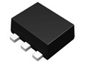
| 供应商器件封装 | 5-HVSOF |
| 其它名称 | BH25PB1WHFV-DKR |
| 包装 | Digi-Reel® |
| 商标 | ROHM Semiconductor |
| 回动电压—最大值 | 600 mV |
| 安装类型 | 表面贴装 |
| 安装风格 | SMD/SMT |
| 封装 | Reel |
| 封装/外壳 | 5-HVSOF |
| 封装/箱体 | HVSOF-5 |
| 工作温度 | -40°C ~ 85°C |
| 工厂包装数量 | 3000 |
| 最大功率耗散 | 0.41 W |
| 最大工作温度 | + 85 C |
| 最大输入电压 | 5.5 V |
| 最小工作温度 | - 40 C |
| 最小输入电压 | 1.7 V |
| 标准包装 | 1 |
| 特色产品 | http://www.digikey.com/product-highlights/cn/zh/rohm-cmos-ldo-regulators/2469 |
| 电压-跌落(典型值) | 0.315V @ 150mA |
| 电压-输入 | 最高 5.5V |
| 电压-输出 | 2.5V |
| 电压调节准确度 | 1 % |
| 电流-输出 | 150mA |
| 电流-限制(最小值) | 160mA |
| 稳压器拓扑 | 正,固定式 |
| 稳压器数 | 1 |
| 线路调整率 | 20 mV |
| 负载调节 | 10 mV |
| 输出电压 | 2.5 V |
| 输出电流 | 150 mA |
| 输出端数量 | 1 Output |
| 输出类型 | Fixed |


- 商务部:美国ITC正式对集成电路等产品启动337调查
- 曝三星4nm工艺存在良率问题 高通将骁龙8 Gen1或转产台积电
- 太阳诱电将投资9.5亿元在常州建新厂生产MLCC 预计2023年完工
- 英特尔发布欧洲新工厂建设计划 深化IDM 2.0 战略
- 台积电先进制程称霸业界 有大客户加持明年业绩稳了
- 达到5530亿美元!SIA预计今年全球半导体销售额将创下新高
- 英特尔拟将自动驾驶子公司Mobileye上市 估值或超500亿美元
- 三星加码芯片和SET,合并消费电子和移动部门,撤换高东真等 CEO
- 三星电子宣布重大人事变动 还合并消费电子和移动部门
- 海关总署:前11个月进口集成电路产品价值2.52万亿元 增长14.8%


PDF Datasheet 数据手册内容提取
CMOS LDO Regulators for Portable Equipments 1ch 150mA CMOS LDO Regulators BH□□PB1WHFV Series No.11020EBT05 ●Description The BH□□PB1WHFV regulator series can respond to changes in output current by switching to a state in which regulator characteristics are ideal. The regulators cut power consumption by lowering their own current consumption to approximately 2 A when the application is operating in the standby state. During normal-current operation it will automatically switch to high-speed operating mode. The IC's soft start function reduce the rush current that flows to the output capacitors during startup. The HVSOF5 package, which features excellent heat dissipation, contributes to space-saving application designs. ●Features 1) Automatic switching between low-consumption and high-speed modes 2) Built-in rush current prevention circuit 3) Low-voltage 1.7 V operation 4) High accuracy output voltage: ± 1% 5) Circuit current during low-consumption operation: 2 A 6) Stable with a ceramic capacitor (0.47 µF) 7) Built-in temperature and overcurrent protection circuits 8) Built-in output discharge during standby operation function 9) Ultra-small HVSOF5 power package ●Applications Battery-driven portable devices, etc. ●Product lineup 150 mA BH□□PB1WHFV Series Product name 1.2 1.5 1.8 2.5 2.8 2.9 3.0 3.1 3.3 Package BH□□PB1WHFV √ √ √ √ √ √ √ √ √ HVSOF5 Model name: BH□□PB1W□ a b Symbol Description Output voltage specification □□ Output voltage (V) □□ Output voltage (V) 12 1.2 V (Typ.) 29 2.9 V (Typ.) 15 1.5 V (Typ.) 30 3.0 V (Typ.) a 18 1.8 V (Typ.) 31 3.1 V (Typ.) 25 2.5 V (Typ.) 33 3.3 V (Typ.) 28 2.8 V (Typ.) b Package HFV: HVSOF5 www.rohm.com 1/10 2011.01 - Rev.B © 2011 ROHM Co., Ltd. All rights reserved.
BH□□PB1WHFV Series Technical Note ●Absolute maximum ratings (Ta = 25°C) Parameter Symbol Ratings Unit Power supply voltage VMAX −0.3 to +6.5 V Power dissipation Pd 410 *1 mW Operating temperature range Topr −40 to +85 °C Storage temperature range Tslg −55 to +125 °C Junction temperature Tjmax 125 °C *1: Reduced by 4.1 mW/°C over 25°C, when mounted on a glass epoxy board (70 mm 70 mm 1.6 mm) ●Recommended operating ranges (not to exceed Pd) Parameter Symbol Ratings Unit Power supply voltage VIN 1.7 to 5.5 V Output MAX current IMAX 0 to 150 mA ●Recommended operating conditions Ratings Parameter Symbol Unit Conditions Min. Typ. Max. The use of ceramic capacitors is Input capacitor CIN 0.33 *2 0.47 − µF recommended. The use of ceramic capacitors is Output capacitor CO 0.33 *2 0.47 − µF recommended. *2: Make sure that the output capacitor value is not kept lower than this specified level across a variety of temperature, DC bias characteristic. And also make sure that the capacitor value can not change as time progresses. www.rohm.com 2/10 2011.01 - Rev.B © 2011 ROHM Co., Ltd. All rights reserved.
BH□□PB1WHFV Series Technical Note ●Electrical characteristics (Unless otherwise specified, Ta = 25°C, VIN = VOUT + 1.0 V, STBY = 1.5 V, SEL = 0 V, CIN = 0.47 µF, CO = 0.47 µF) Limits Parameter Symbol Unit Conditions Min. Typ. Max.. 【Regulator】 VOUT1 VOUT1 - V VOUT≧2.5V,IOUT=0.1mA,SEL=1.5V Output voltage ×0.99 ×1.01 VOUT1 (high-speed mode) VOUT1 VOUT1 - V VOUT≦1.8V,IOUT=0.1mA,SEL=1.5V -0.025 +0.025 VOUT2 VOUT2 - V VOUT≧2.5V,IOUT=0.1mA,SEL=0V Output voltage ×0.97 ×1.038 VOUT2 (low-consumption mode) VOUT2 VOUT2 - V VOUT≦1.8V,IOUT=0.1mA,SEL=0V ×0.967 ×1.043 Circuit current IOUT=0mA, VIN pin ICC1 - 20 40 μA (high-speed mode) monitor,SEL=1.5V Circuit current ICC2 - 2 4 μA IOUT=0mA, VIN pin monitor, SEL=0V (low-consumption mode) Circuit current (STBY) ISTBY - - 1.0 μA STBY=0V Ripple rejection ratio VRR=-20dBv, fRR=1kHz, RR1 42 60 - dB (high-speed mode) IOUT=10mA, SEL=1.5V Dropout voltage 1 *1 VSAT1 - 100 200 mV VIN=VOUT×0.98,IOUT=50mA Dropout voltage 2 *1 VSAT2 - 210 400 mV VIN=VOUT×0.98,IOUT=100mA Dropout voltage 3 *1 VSAT3 - 315 600 mV VIN=VOUT×0.98,IOUT=150mA Line regulation 1 VDL1 - 2 20 mV VIN=VOUT+1V to 5.5V,IOUT=10mA (high-speed mode) Line regulation 2 VDL2 - 2 20 mV VIN=VOUT+1V to 5.5V,IOUT=100μA (low-consumption mode) Load regulation VDLO - 10 40 mV IOUT=10mA to 100mA 【Mode switch】 Current threshold ITH1 0.09 0.3 - mA SEL=0V IOUT=3mA⇒0mA sweep (low-consumption mode) Current threshold ITH2 - 1.2 2.2 mA SEL=0V IOUT=0mA⇒3mA sweep (high-speed mode) 【Over Current Protection 1】 Limit Current ILMAX 160 300 500 mA Vo=VOUT×0.90 Short current ISHORT 20 50 100 mA Vo=0V 【Stand-by block】 STBY pin sink current ISTB - 2 4 μA STBY=1.5V ON VSTBH 1.5 - VIN V STBY control voltage OFF VSTBL -0.3 - 0.3 V Discharge resistance at standby RDCG 1.5 2.2 3.0 kΩ STBY=0V 【SEL PIN】 Pull-down resistance of SEL pin RSEL 0.5 1.0 2.0 MΩ ON VSELH 1.5 - VIN V Fixed high speed mode SEL control voltage OFF VSELL -0.3 - 0.3 V Automatic switch mode * Note: This IC is not designed to be radiation-resistant. *3: Except at VOUT ≤ 1.5 V. ●Electrical characteristics of each output voltage Output Voltage Parameter Min. Typ. Max. Unit Conditions 70 120 − VCC = 1.7 V 1.2 V 150 − − VCC = 2.0 V Max. output 50 100 − VCC = 1.8 V 1.5 V mA current 150 − − VCC = 2.2 V 75 143 − VCC = VOUT + 0.3 V 1.8 V ≤ VOUT 150 − − VCC = VOUT + 0.6 V www.rohm.com 3/10 2011.01 - Rev.B © 2011 ROHM Co., Ltd. All rights reserved.
BH□□PB1WHFV Series Technical Note ●Typical characteristics 4.0 4.0 4.0 3.5 3.5 3.5 Output Voltage VOUT [V]11223.....05050 Output Voltage VOUT [V]11223.....05050 Output Voltage VOUT [V]11223.....05050 0.5 IO = 10 mA 0.5 IO = 10 mA 0.5 IO = 10 mA 0.0 0.0 0.0 0 1 Input2 Voltag3e VIN 4[V] 5 0 1 Inpu2t Voltag3e VIN [4V] 5 0 1 Inp2ut Volta3ge VIN 4 [V] 5 Fig.1 Output Voltage vs Input Voltage Fig.2 Output Voltage vs Input Voltage Fig.3 Output Voltage vs Input Voltage (BH12PB1WHFV) (BH30PB1WHFV) (BH33PB1WHFV) 70 3.5 400 60 IO = no load 3.0 IO = no load AT IO = no load S urrent IGND [μA]345000 SEL = 1.5 V Voltage VOUT [V]122...505 SEL = 1.5 V oltage difference V[mV]230000 SEL = 1.5 V GND C20 Output 1.0 Output V 100 10 SEL = 0 V 0.5 SEL = 0 V nput SEL = 0 V 0 0.0 I 0 0 1 2 3 4 5 0 100 200 300 400 0 50 100 150 Input Voltage VIN [V] Output Current IOUT [mA] Output Current IOUT [mA] (BH30PB1WHFV) (BH33PB1WHFV) Fig.6 GND Current vs-Input Voltage (BH12PB1WHFV) (BH33PB1WHFV) (BH30PB1WHFV) 3.5 3.5 3.5 3.0 3.0 3.0 UT [V]2.5 UT [V]2.5 UT [V]2.5 Output Voltage VO112...050 Output Voltage VO112...050 Output Voltage VO112...050 0.5 0.5 0.5 0.0 0.0 0.0 0 100 200 300 400 0 100 200 300 400 0 100 200 300 400 Output Current IOUT [mA] Output Current IOUT [mA] Output Current IOUT [mA] (BH30PB1WHFV) Fig.8 Output Voltage vs Output Current Fig.9 Output Voltage vs Output Current (BH12PB1WHFV) (BH30PB1WHFV) (BH33PB1WHFV) 3.5 400 400 T T Output Voltage VOUT [V] 11223.....05050 Output Voltage difference VOU[mV]123000000 Output Voltage difference VSA[mV]123000000 00..05 Input 0 Input 0 0 100 200 300 400 0 50 100 150 0 50 100 150 Output Current IOUT [mA] Output Current IOUT [mA] Output Current IOUT [mA] Fig.10 Dropout voltage vs Output Current Fig.11Dropout voltage vs Output Current Fig.12 Dropout voltage vs Output Current (BH18PB1WHFV) (BH30PB1WHFV) (BH33PB1WHFV) www.rohm.com 4/10 2011.01 - Rev.B © 2011 ROHM Co., Ltd. All rights reserved.
BH□□PB1WHFV Series Technical Note 3.2 4 6 A] µ Y[5 Output Voltage VOUT[V]233...901 Output Voltage VOUT[V]123 by Pin Sink Current ISTB234 and1 St 2.8 0 0 -50 -25 0 25 50 75 100 0.0 0.5 1.0 1.5 2.0 0.0 1.0 2.0 3.0 4.0 5.0 Temp[℃] VSTBY[V] VSTBY[V] Fig.13 Output Voltage vs Temperature Fig.14 Standby Pin Threshold Fig.15 Standby Pin Sink Current (BH30PB1WHFV) (BH30PB1WHFV) (BH30PB1WHFV) 80 80 70 70 B] B] SEL SEL = 0 V 1.5 1 V / div R.[d60 R.[d60 R. R. Ripple Rejection 345000 Ripple Rejection 345000 VOUT 50 mV / div Co = 0.47 µF Co = 0.47 µF 20 IO = 10 mA 20 IO = 10 mA IO = no load 10 ms / div 10 10 100 1 k 10 k 100 1 M 100 1 k 10 k 100 1 M Frequency f[Hz] Frequency f[Hz] Fig.16 Ripple Rejection Fig.17 Ripple Rejection Fig.18 Output Voltage Waveform (BH12PB1WHFV) (BH30PB1WHFV) During SEL Switching (BH30PB1WHFV) IOUT = 0 mA 10 mA IOUT = 1 mA 30 mA IOUT = 1 mA 100 50 mV / div 50 mV / div 100 mV / div VOUT VOUT VOUT SEL = 0 V (power-saving operation) 100 s / div SEL = 1.5 V 200 s / div 200 s / div Fig.19 Load Response (Co = 1.0 µF) Fig.20 Load Response (Co=1.0 µF) Fig.21 Load Response (Co=1.0 µF) (BH30PB1WHFV) (BH30PB1WHFV) (BH30PB1WHFV) 100 m 1 V / div Rss = 10 k, STBY STBY 1 V / div IO = no load e [sec]10 m s 1 V / div VOUT Tri e Co = 0.47 µF CCCooo === 201.. 24µ 7Fµ µFF Startup tim1.0µ VOUT Co = 10 µF 1 V / div 200 s / div 10 ms / div 100 µ 0.01µ 0.1 µ 1.0µ Slow start capacitance Css (F) Fig.22 Output Voltage Rise Time Fig.23 Output Voltage Fall Time Fig.24 Soft Start Rise Time (BH30PB1WHFV) (BH30PB1WHFV) (BH30PB1WHFV) www.rohm.com 5/10 2011.01 - Rev.B © 2011 ROHM Co., Ltd. All rights reserved.
BH□□PB1WHFV Series Technical Note ●Block diagram, recommended circuit diagram, and pin assignment table BH□□PB1WHFV PIN No. Symbol Function 1 STBY Output voltage on/off control(High: ON, Low: OFF) 2 GND Ground 3 VIN Power supply input 4 VOUT Voltage output Mode switching 5 SEL (High: Fix in high-speed mode Low: Automatic low-consumption mode switching) VIN 3 CH1 - - + Cin VOLTAGE OVTEHRE RCMUARLR E&NT VOUT GND REFERENCE PROTECTION 4 2 - Co - + CH2 SOFFT DISCHARGE Cin … 0.47 µF START Co … 0.47 µF STBY(R s s )( ) 1 COBLNOTCRKOL CMUORNRIETNOTR 5 SEL Css Fig.25 ●Auto Power-saving Function The IC incorporates a built-in auto power-saving function that 30 continuously monitors the output current and switches μA] Measurement conditions automatically between a low current consumption regulator D [ High-speed mode N 20 BH12PB1WHFV and a high-speed operation regulator. This function reduces G the regulator's own current consumption to approximately 1/10 ntI VCC = 2.2 V e or lower of normal levels when the output current falls below urr 10 VSEL = open, c approximately 300 A. D To operate only the high-speed operation regulator without GN 0 Low-consumption mode VSTBY = 1.5 V using the auto power-saving function, fix the SEL pin to high. 0 0.5 1 1.5 2 2.5 3 Output current IOUT [mA] Fig.26 Auto Power-Saving Function (Example) ●Power Dissipation (Pd) 1. Power Dissipation (Pd) 2. Power Dissipation/Heat Reduction (Pd) Power dissipation calculations include estimates of power HVSOF5 dissipation characteristics and internal IC power consumption, and 0.6 *Circuit design should be treated as guidelines. In the event that the IC is used in should allow a 410 mW an environment where this power dissipation is exceeded, the sufficient attendant rise in the junction temperature will trigger the thermal margin for the 0.4 temperature shutdown circuit, reducing the current capacity and otherwise range so that degrading the IC's design performance. Allow for sufficient margins W] PMAX < Pd. d[ so that this power dissipation is not exceeded during IC operation. P 0.2 Calculating the maximum internal IC power consumption (PMAX) 0 0 25 50 75 100 125 Ta[℃] PMAX = (VIN - VOUT) IOUT (MAX.) VIN : Input voltage Fig.27 HVSOF5 Power Dissipation VOUT : Output voltage vs Heat Reduction (Example) IOUT (MAX) : Max. output current www.rohm.com 6/10 2011.01 - Rev.B © 2011 ROHM Co., Ltd. All rights reserved.
BH□□PB1WHFV Series Technical Note ●Input Output capacitors It is recommended to insert bypass capacitors between input and GND pins, positioning them as close to the pins as possible. These capacitors will be used when the power supply impedance increases or when long wiring paths are used, so they should be checked once the IC has been mounted. Ceramic capacitors generally have temperature and DC bias characteristics. When selecting ceramic capacitors, use X5R or X7R, or better models that offer good temperature and DC bias characteristics and high tolerant voltages. Typical ceramic capacitor characteristics 120 100 120 50 V rated voltage Capacitance rate of change (%)124680000000 1ra0tVed v oltage 16 5V0 rVat eradt evdo lvtaogltea ge Capacitance rate of change (%)778899050505 1ra0t eVd voltag1e6 V rated voltage Capacitance rate of change (%)124680000000 Y5V XX57RR 0 1 DC bias 2Vdc (V) 3 4 0 1 DC bias 2Vdc (V) 3 4 -25 0 Tem2p5[℃] 50 75 Fig.28 Capacitance vs Bias Fig.29 Capacitance vs Bias Fig.30 Capacitance vs Temperature (Y5V) (X5R, X7R) (X5R, X7R, Y5V) ●Output capacitors Mounting input capacitor between input pin and GND(as close to pin as possible), and also output capacitor between output pin and GND(as close to pin as possible) is recommended. The input capacitor reduces the output impedance of the voltage supply source connected to the VCC. The higher value the output capacitor goes the more stable the whole operation becomes. This leads to high load transient response. Please confirm the whole operation on actual application board. Generally, ceramic capacitor has wide range of tolerance, temperature coefficient, and DC bias characteristic. And also its value goes lower as time progresses. Please choose ceramic capacitors after obtaining more detailed data by asking capacitor makers. BH□□PB1WHFV 100 10 Ω) SR ( 1 Stable region E COUT = 0.47 µF Ta = +25°C 0.1 0.01 0 50 100 150 Output Current Io (mA) Fig.31 Stable Operation Region (Example) www.rohm.com 7/10 2011.01 - Rev.B © 2011 ROHM Co., Ltd. All rights reserved.
BH□□PB1WHFV Series Technical Note ●Notes for use 1. Absolute maximum ratings An excess in the absolute maximum ratings, such as supply voltage, temperature range of operating conditions, etc., can break down the devices, thus making impossible to identify breaking mode, such as a short circuit or an open circuit. If any over rated values will expect to exceed the absolute maximum ratings, consider adding circuit protection devices, such as fuses. 2. Thermal design Use a thermal design that allows for a sufficient margin in light of the power dissipation (Pd) in actual operating conditions. 3. Inter-pin shorts and mounting errors Use caution when positioning the IC for mounting on printed circuit boards. The IC may be damaged if there is any connection error or if pins are shorted together. 4. Thermal shutdown circuit (TSD) The IC incorporates a built-in thermal shutdown circuit (TSD circuit). The thermal shutdown circuit is designed only to shut the IC off to prevent runaway thermal operation. It is not designed to protect the IC or guarantee its operation. Do not continue to use the IC after operating this circuit or use the IC in an environment where the operation of this circuit is assumed. 5. Ground wiring patterns The power supply and ground lines must be as short and thick as possible to reduce line impedance. Fluctuating voltage on the power ground line may damage the device. 6. Overcurrent protection circuit The IC incorporates a built-in overcurrent protection circuit that operates according to the output current capacity. This circuit serves to protect the IC from damage when the load is shorted. The protection circuit is designed to limit current flow by not latching in the event of a large and instantaneous current flow originating from a large capacitor or other component. These protection circuits are effective in preventing damage due to sudden and unexpected accidents. However, the IC should not be used in applications characterized by the continuous operation or transitioning of the protection circuits. At the time of thermal designing, keep in mind that the current capability has negative characteristics to temperatures. 7. Actions in strong electromagnetic field Use caution when using the IC in the presence of a strong electromagnetic field as doing so may cause the IC to malfunction. 8. Back current In applications where the IC may be exposed to back current flow, it is recommended to create a path to dissipate this current by inserting a bypass diode between the VIN and VOUT pins. Back current VIN OUT STBY GND Fig.32 Example Bypass Diode Connection 9. I/O voltage difference Using the IC in automatic switching mode when the I/O voltage differential becomes saturated (VIN - VOUT < 150 mV) may result in a large output noise level. If the noise level becomes problematic, use the IC with the SEL pin in the high state when the voltage differential is saturated. 10. GND Voltage The potential of GND pin must be minimum potential in all operating conditions. www.rohm.com 8/10 2011.01 - Rev.B © 2011 ROHM Co., Ltd. All rights reserved.
BH□□PB1WHFV Series Technical Note 11. Preventing Rush Current By attaching the Rss and Css time constants to the STBY pin, sudden rises in the regulator output voltage can be prevented, dampening the flow of rush current to the output capacitors. The larger the time constant used, the greater the resulting reduction. However, large time constants also result in longer startup times, so the constant should be selected after considering the conditions in which the IC is to be used. 100 Rss = 10 k IO = no load Trise [sec]10 間me 起動時Startup ti1.0 m 100 0.01 0.1 1.0 Slow sFtarret qcuaepnaccyit af[nHcze] Css (F) Fig.33 VOUT Startup Time vs CSS Capacitance (Reference) 12. Regarding input Pin of the IC (Fig.34) This monolithic IC contains P+ isolation and P substrate layers between adjacent elements in order to keep them isolated. P-N junctions are formed at the intersection of these P layers with the N layers of other elements, creating a parasitic diode or transistor. For example, the relation between each potential is as follows: When GND > Pin A and GND > Pin B, the P-N junction operates as a parasitic diode. When GND > Pin B, the P-N junction operates as a parasitic transistor. Parasitic diodes can occur inevitable in the structure of the IC. The operation of parasitic diodes can result in mutual interference among circuits, operational faults, or physical damage. Accordingly, methods by which parasitic diodes operate, such as applying a voltage that is lower than the GND (P substrate) voltage to an input pin, should not be used. Resistor Transistor (NPN) Pin A Pin B B Pin B C E Pin A B C N N P+ N N P+ P P+ N Parasitic P P+ N E element Parasitic P substrate P substrate element GND GND GND GND Parasitic element Parasitic element Other adjacent elements Fig.34 www.rohm.com 9/10 2011.01 - Rev.B © 2011 ROHM Co., Ltd. All rights reserved.
BH□□PB1WHFV Series Technical Note ●Ordering part number B H 3 0 P B 1 W H F V - T R Part No. Output voltage Series Shutdown Package Packaging and forming specification 12: 1.2 V PB1:Auto power- switch HFV : HVSOF5 TR: Embossed tape and reel 15: 1.5 V saving type W : Includes 18: 1.8 V switch 25: 2.5 V 28: 2.8 V 29: 2.9 V 30: 3.0 V 31: 3.1 V 33: 3.3 V HVSOF5 <Tape and Reel information> 1.6±0.05 (0.8) Tape Embossed carrier tape ±1.60.05 ±1.20.05X 1.28 include BURR)(0.05) 1.150±20.4035 (0.91) (0.41) 34(02.31)5 0.0.2MAX13±0.05 QDofiu rfeaecnettdiiotyn 3T(0RTre0he0elp odcnirs ethcetio lenf tis h tahned 1 apnind oyfo pur opduull cot uist tah1te pt htianep uep opne rt hrieg hritg whth heann ydou hold ) A M ( X S A M 0.6 +0.03–0.02 0.5 0.1 S 0.02 0.22±0.05 0.08M Direction of feed (Unit : mm) Reel ∗ Order quantity needs to be multiple of the minimum quantity. www.rohm.com 10/10 2011.01 - Rev.B © 2011 ROHM Co., Ltd. All rights reserved.
DDaattaasshheeeett Notice Precaution on using ROHM Products 1. Our Products are designed and manufactured for application in ordinary electronic equipments (such as AV equipment, OA equipment, telecommunication equipment, home electronic appliances, amusement equipment, etc.). If you intend to use our Products in devices requiring extremely high reliability (such as medical equipment (Note 1), transport equipment, traffic equipment, aircraft/spacecraft, nuclear power controllers, fuel controllers, car equipment including car accessories, safety devices, etc.) and whose malfunction or failure may cause loss of human life, bodily injury or serious damage to property (“Specific Applications”), please consult with the ROHM sales representative in advance. Unless otherwise agreed in writing by ROHM in advance, ROHM shall not be in any way responsible or liable for any damages, expenses or losses incurred by you or third parties arising from the use of any ROHM’s Products for Specific Applications. (Note1) Medical Equipment Classification of the Specific Applications JAPAN USA EU CHINA CLASSⅢ CLASSⅡb CLASSⅢ CLASSⅢ CLASSⅣ CLASSⅢ 2. ROHM designs and manufactures its Products subject to strict quality control system. However, semiconductor products can fail or malfunction at a certain rate. Please be sure to implement, at your own responsibilities, adequate safety measures including but not limited to fail-safe design against the physical injury, damage to any property, which a failure or malfunction of our Products may cause. The following are examples of safety measures: [a] Installation of protection circuits or other protective devices to improve system safety [b] Installation of redundant circuits to reduce the impact of single or multiple circuit failure 3. Our Products are designed and manufactured for use under standard conditions and not under any special or extraordinary environments or conditions, as exemplified below. Accordingly, ROHM shall not be in any way responsible or liable for any damages, expenses or losses arising from the use of any ROHM’s Products under any special or extraordinary environments or conditions. If you intend to use our Products under any special or extraordinary environments or conditions (as exemplified below), your independent verification and confirmation of product performance, reliability, etc, prior to use, must be necessary: [a] Use of our Products in any types of liquid, including water, oils, chemicals, and organic solvents [b] Use of our Products outdoors or in places where the Products are exposed to direct sunlight or dust [c] Use of our Products in places where the Products are exposed to sea wind or corrosive gases, including Cl2, H2S, NH3, SO2, and NO2 [d] Use of our Products in places where the Products are exposed to static electricity or electromagnetic waves [e] Use of our Products in proximity to heat-producing components, plastic cords, or other flammable items [f] Sealing or coating our Products with resin or other coating materials [g] Use of our Products without cleaning residue of flux (even if you use no-clean type fluxes, cleaning residue of flux is recommended); or Washing our Products by using water or water-soluble cleaning agents for cleaning residue after soldering [h] Use of the Products in places subject to dew condensation 4. The Products are not subject to radiation-proof design. 5. Please verify and confirm characteristics of the final or mounted products in using the Products. 6. In particular, if a transient load (a large amount of load applied in a short period of time, such as pulse. is applied, confirmation of performance characteristics after on-board mounting is strongly recommended. Avoid applying power exceeding normal rated power; exceeding the power rating under steady-state loading condition may negatively affect product performance and reliability. 7. De-rate Power Dissipation (Pd) depending on Ambient temperature (Ta). When used in sealed area, confirm the actual ambient temperature. 8. Confirm that operation temperature is within the specified range described in the product specification. 9. ROHM shall not be in any way responsible or liable for failure induced under deviant condition from what is defined in this document. Precaution for Mounting / Circuit board design 1. When a highly active halogenous (chlorine, bromine, etc.) flux is used, the residue of flux may negatively affect product performance and reliability. 2. In principle, the reflow soldering method must be used; if flow soldering method is preferred, please consult with the ROHM representative in advance. For details, please refer to ROHM Mounting specification Notice - GE Rev.002 © 2014 ROHM Co., Ltd. All rights reserved.
DDaattaasshheeeett Precautions Regarding Application Examples and External Circuits 1. If change is made to the constant of an external circuit, please allow a sufficient margin considering variations of the characteristics of the Products and external components, including transient characteristics, as well as static characteristics. 2. You agree that application notes, reference designs, and associated data and information contained in this document are presented only as guidance for Products use. Therefore, in case you use such information, you are solely responsible for it and you must exercise your own independent verification and judgment in the use of such information contained in this document. ROHM shall not be in any way responsible or liable for any damages, expenses or losses incurred by you or third parties arising from the use of such information. Precaution for Electrostatic This Product is electrostatic sensitive product, which may be damaged due to electrostatic discharge. Please take proper caution in your manufacturing process and storage so that voltage exceeding the Products maximum rating will not be applied to Products. Please take special care under dry condition (e.g. Grounding of human body / equipment / solder iron, isolation from charged objects, setting of Ionizer, friction prevention and temperature / humidity control). Precaution for Storage / Transportation 1. Product performance and soldered connections may deteriorate if the Products are stored in the places where: [a] the Products are exposed to sea winds or corrosive gases, including Cl2, H2S, NH3, SO2, and NO2 [b] the temperature or humidity exceeds those recommended by ROHM [c] the Products are exposed to direct sunshine or condensation [d] the Products are exposed to high Electrostatic 2. Even under ROHM recommended storage condition, solderability of products out of recommended storage time period may be degraded. It is strongly recommended to confirm solderability before using Products of which storage time is exceeding the recommended storage time period. 3. Store / transport cartons in the correct direction, which is indicated on a carton with a symbol. Otherwise bent leads may occur due to excessive stress applied when dropping of a carton. 4. Use Products within the specified time after opening a humidity barrier bag. Baking is required before using Products of which storage time is exceeding the recommended storage time period. Precaution for Product Label QR code printed on ROHM Products label is for ROHM’s internal use only. Precaution for Disposition When disposing Products please dispose them properly using an authorized industry waste company. Precaution for Foreign Exchange and Foreign Trade act Since our Products might fall under controlled goods prescribed by the applicable foreign exchange and foreign trade act, please consult with ROHM representative in case of export. Precaution Regarding Intellectual Property Rights 1. All information and data including but not limited to application example contained in this document is for reference only. ROHM does not warrant that foregoing information or data will not infringe any intellectual property rights or any other rights of any third party regarding such information or data. ROHM shall not be in any way responsible or liable for infringement of any intellectual property rights or other damages arising from use of such information or data.: 2. No license, expressly or implied, is granted hereby under any intellectual property rights or other rights of ROHM or any third parties with respect to the information contained in this document. Other Precaution 1. This document may not be reprinted or reproduced, in whole or in part, without prior written consent of ROHM. 2. The Products may not be disassembled, converted, modified, reproduced or otherwise changed without prior written consent of ROHM. 3. In no event shall you use in any way whatsoever the Products and the related technical information contained in the Products or this document for any military purposes, including but not limited to, the development of mass-destruction weapons. 4. The proper names of companies or products described in this document are trademarks or registered trademarks of ROHM, its affiliated companies or third parties. Notice - GE Rev.002 © 2014 ROHM Co., Ltd. All rights reserved.
DDaattaasshheeeett General Precaution 1. Before you use our Products, you are requested to carefully read this document and fully understand its contents. ROHM shall not be in any way responsible or liable for failure, malfunction or accident arising from the use of a ny ROHM’s Products against warning, caution or note contained in this document. 2. All information contained in this document is current as of the issuing date and subj ect to change without any prior notice. Before purchasing or using ROHM’s Products, please confirm the latest information with a ROHM sale s representative. 3. The information contained in this document is provided on an “as is” basis and ROHM does not warrant that all information contained in this document is accurate an d/or error-free. ROHM shall not be in any way responsible or liable for any damages, expenses or losses incurred by you or third parties resulting from inaccuracy or errors of or concerning such information. Notice – WE Rev.001 © 2014 ROHM Co., Ltd. All rights reserved.