ICGOO在线商城 > 集成电路(IC) > 嵌入式 - 微控制器 > MC9S08QG4CPBE
 Datasheet下载
- 型号: MC9S08QG4CPBE
- 制造商: Freescale Semiconductor
- 库位|库存: xxxx|xxxx
- 要求:
| 数量阶梯 | 香港交货 | 国内含税 |
| +xxxx | $xxxx | ¥xxxx |
查看当月历史价格
查看今年历史价格
MC9S08QG4CPBE产品简介:
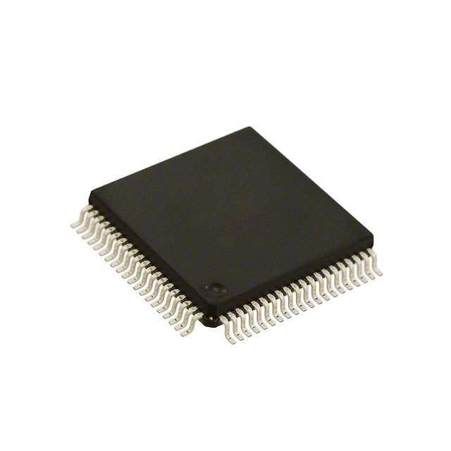
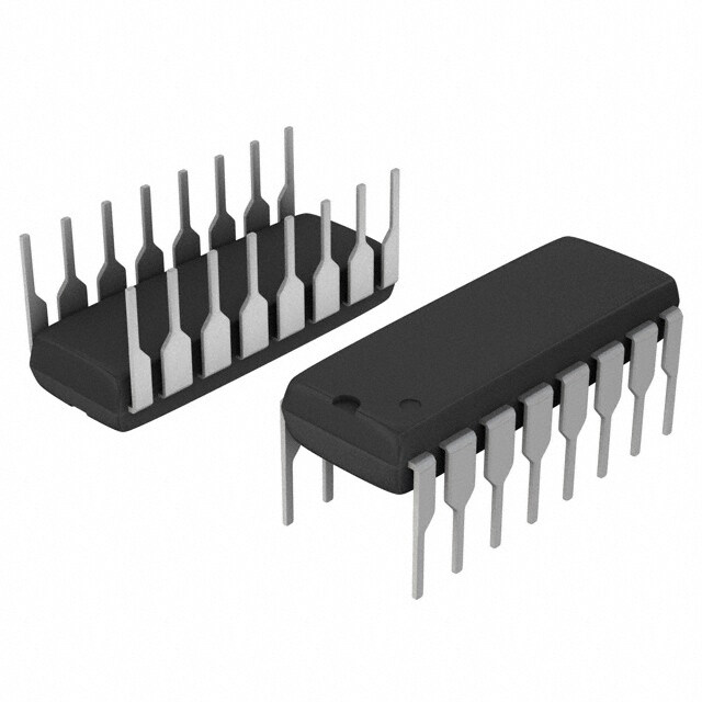
ICGOO电子元器件商城为您提供MC9S08QG4CPBE由Freescale Semiconductor设计生产,在icgoo商城现货销售,并且可以通过原厂、代理商等渠道进行代购。 MC9S08QG4CPBE价格参考。Freescale SemiconductorMC9S08QG4CPBE封装/规格:嵌入式 - 微控制器, S08 微控制器 IC S08 8-位 20MHz 4KB(4K x 8) 闪存 16-DIP。您可以下载MC9S08QG4CPBE参考资料、Datasheet数据手册功能说明书,资料中有MC9S08QG4CPBE 详细功能的应用电路图电压和使用方法及教程。
型号为MC9S08QG4CPBE的嵌入式微控制器由NXP USA Inc.生产,属于低成本、低功耗的8位微控制器系列。该芯片主要面向对成本敏感且功能相对简单的嵌入式控制应用。

其典型应用场景包括:

1. 消费类电子产品:如小家电(电饭煲、微波炉、风扇等)中的控制面板,实现按键输入、LED显示和简单逻辑控制。

2. 工业控制:用于传感器信号采集、开关控制、电机控制等基础自动化任务,例如在小型泵、风扇或继电器控制系统中使用。

3. 汽车电子:适用于车身控制模块(如车窗、门锁、灯光控制)等对性能要求不高的场合。

4. 智能仪表:如电表、水表、燃气表等,用于数据采集与显示控制。

5. 家用安防设备:如门禁控制器、简易报警系统等。

MC9S08QG4CPBE具有4KB Flash存储器和128B RAM,适合运行轻量级程序,配合其低功耗特性,适合电池供电或对能效有要求的应用场景。其封装为20引脚DIP或SOIC,易于焊接和集成,适合中小规模批量生产。
| 参数 | 数值 |
| 产品目录 | 集成电路 (IC)半导体 |
| 描述 | IC MCU 8BIT 4KB FLASH 16DIP8位微控制器 -MCU CONSUMER ROO 9S08QG |
| EEPROM容量 | - |
| 产品分类 | |
| I/O数 | 12 |
| 品牌 | Freescale Semiconductor |
| 产品手册 | |
| 产品图片 |
|
| rohs | 符合RoHS无铅 / 符合限制有害物质指令(RoHS)规范要求 |
| 产品系列 | 嵌入式处理器和控制器,微控制器 - MCU,8位微控制器 -MCU,Freescale Semiconductor MC9S08QG4CPBES08 |
| 数据手册 | |
| 产品型号 | MC9S08QG4CPBE |
| PCN设计/规格 | http://cache.freescale.com/files/shared/doc/pcn/PCN15684.htm |
| RAM容量 | 256 x 8 |
| 产品培训模块 | http://www.digikey.cn/PTM/IndividualPTM.page?site=cn&lang=zhs&ptm=2193http://www.digikey.cn/PTM/IndividualPTM.page?site=cn&lang=zhs&ptm=3378 |
| 产品目录页面 | |
| 产品种类 | 8位微控制器 -MCU |
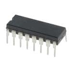
| 供应商器件封装 | 16-DIP |
| 包装 | 管件 |
| 单位重量 | 1.081 g |
| 可编程输入/输出端数量 | 12 |
| 商标 | Freescale Semiconductor |
| 处理器系列 | MC9S08 |
| 外设 | LVD,POR,PWM,WDT |
| 安装风格 | Through Hole |
| 定时器数量 | 1 Timer |
| 封装 | Tube |
| 封装/外壳 | 16-DIP(0.300",7.62mm) |
| 封装/箱体 | PDIP-16 |
| 工作温度 | -40°C ~ 85°C |
| 工作电源电压 | 1.8 V to 3.6 V |
| 工厂包装数量 | 25 |
| 振荡器类型 | 内部 |
| 接口类型 | I2C, SCI, SPI |
| 数据RAM大小 | 256 V |
| 数据总线宽度 | 8 bit |
| 数据转换器 | A/D 8x10b |
| 最大工作温度 | + 85 C |
| 最大时钟频率 | 20 MHz |
| 最小工作温度 | - 40 C |
| 标准包装 | 3,000 |
| 核心 | S08 |
| 核心处理器 | S08 |
| 核心尺寸 | 8-位 |
| 片上ADC | Yes |
| 电压-电源(Vcc/Vdd) | 1.8 V ~ 3.6 V |
| 电源电压-最大 | 3.6 V |
| 电源电压-最小 | 1.8 V |
| 程序存储器大小 | 4 kB |
| 程序存储器类型 | 闪存 |
| 程序存储容量 | 4KB(4K x 8) |
| 系列 | S08QG |
| 输入/输出端数量 | 12 I/O |
| 连接性 | I²C, SCI, SPI |
| 速度 | 20MHz |


PDF Datasheet 数据手册内容提取
Freescale Semiconductor Document Number: QFN_Addendum Rev. 0, 07/2014 Addendum Addendum for New QFN Package Migration This addendum provides the changes to the 98A case outline numbers for products covered in this book. Case outlines were changed because of the migration from gold wire to copper wire in some packages. See the table below for the old (gold wire) package versus the new (copper wire) package. To view the new drawing, go to Freescale.com and search on the new 98A package number for your device. For more information about QFN package use, see EB806: Electrical Connection Recommendations for the Exposed Pad on QFN and DFN Packages. ©Freescale Semiconductor, Inc., 2014. All rights reserved.
Original (gold wire) Current (copper wire) Part Number Package Description package document number package document number MC68HC908JW32 48 QFN 98ARH99048A 98ASA00466D MC9S08AC16 MC9S908AC60 MC9S08AC128 MC9S08AW60 MC9S08GB60A MC9S08GT16A MC9S08JM16 MC9S08JM60 MC9S08LL16 MC9S08QE128 MC9S08QE32 MC9S08RG60 MCF51CN128 MC9RS08LA8 48 QFN 98ARL10606D 98ASA00466D MC9S08GT16A 32 QFN 98ARH99035A 98ASA00473D MC9S908QE32 32 QFN 98ARE10566D 98ASA00473D MC9S908QE8 32 QFN 98ASA00071D 98ASA00736D MC9S08JS16 24 QFN 98ARL10608D 98ASA00734D MC9S08QB8 MC9S08QG8 24 QFN 98ARL10605D 98ASA00474D MC9S08SH8 24 QFN 98ARE10714D 98ASA00474D MC9RS08KB12 24 QFN 98ASA00087D 98ASA00602D MC9S08QG8 16 QFN 98ARE10614D 98ASA00671D MC9RS08KB12 8 DFN 98ARL10557D 98ASA00672D MC9S08QG8 MC9RS08KA2 6 DFN 98ARL10602D 98ASA00735D Addendum for New QFN Package Migration, Rev. 0 2 Freescale Semiconductor
MC9S08QG8 MC9S08QG4 Data Sheet HCS08 Microcontrollers MC9S08QG8 Rev. 5 11/2009 freescale.com
None
MC9S08QG8/4 Features 8-Bit HCS08 Central Processor Unit (CPU) Peripherals • 20-MHz HCS08 CPU (central processor unit) • ADC — 8-channel, 10-bit analog-to-digital • HC08 instruction set with added BGND instruction converter with automatic compare function, • Background debugging system asynchronous clock source, temperature sensor, and internal bandgap reference channel; ADC is • Breakpoint capability to allow single breakpoint hardware triggerable using the RTI counter setting during in-circuit debugging (plus two more breakpoints in on-chip debug module) • ACMP — Analog comparator module with option to compare to internal reference; output can be • Debug module containing two comparators and nine optionally routed to TPM module trigger modes. Eight deep FIFO for storing change-of-flow addresses and event-only data • SCI — Serial communications interface module Debug module supports both tag and force with option for 13-bit break capabilities breakpoints • SPI — Serial peripheral interface module • Support for up to 32 interrupt/reset sources • IIC — Inter-integrated circuit bus module • TPM— 2-channel timer/pulse-width modulator; Memory Options each channel can be used for input capture, output compare, buffered edge-aligned PWM, or buffered • FLASH read/program/erase over full operating center-aligned PWM voltage and temperature • MTIM — 8-bit modulo timer module with 8-bit • MC9S08QG8 — 8 Kbytes FLASH, 512 bytes RAM prescaler MC9S08QG4 — 4 Kbytes FLASH, 256 bytes RAM • KBI — 8-pin keyboard interrupt module with software Power-Saving Modes selectable polarity on edge or edge/level modes Input/Output • Wait plus three stops Clock Source Options • 12 general-purpose input/output (I/O) pins, one input-only pin and one output-only pin; outputs • ICS — Internal clock source module containing a 10mA each, 60 mA max for package frequency-locked-loop (FLL) controlled by internal • Software selectable pullups on ports when used as or external reference; precision trimming of internal input reference allows 0.2% resolution and 2% deviation • Software selectable slew rate control and drive over temperature and voltage; supports bus strength on ports when used as output frequencies from 1 MHz to 10 MHz • Internal pullup on RESET and IRQ pins to reduce • XOSC — Low-power oscillator module with customer system cost software selectable crystal or ceramic resonator range, 31.25 kHz to 38.4 kHz or 1 MHz to 16 MHz, Development Support and supports external clock source input up to 20MHz • Single-wire background debug interface • On-chip, in-circuit emulation (ICE) with real-time System Protection bus capture • Watchdog computer operating properly (COP) reset Package Options with option to run from dedicated 1-kHz internal clock source or bus clock • 24-pin quad flat no lead (QFN) package • Low-voltage detection with reset or interrupt • 16-pin plastic dual in-line package (PDIP) — • Illegal opcode detection with reset MC9S08QG8 only • Illegal address detection with reset • 16-pin quad flat no lead (QFN) package • FLASH block protect • 16-pin thin shrink small outline package (TSSOP) • 8-pin dual flat no lead (DFN) package • 8-pin PDIP — MC9S08QG4 only • 8-pin narrow body small outline integrated circuit (SOIC) package
None
MC9S08QG8 Data Sheet Covers MC9S08QG8 MC9S08QG4 MC9S08QG8 Rev. 5 11/2009 Freescale™ and the Freescale logo are trademarks of Freescale Semiconductor, Inc. ©Freescale Semiconductor, Inc., 2007-2009. All rights reserved.
Revision History To provide the most up-to-date information, the revision of our documents on the World Wide Web will be the most current. Your printed copy may be an earlier revision. To verify you have the latest information available, refer to: http://freescale.com/ The following revision history table summarizes changes contained in this document. Rev Revision Description of Changes No. Date Previous version was 1.01; revision numbering will increment by integers from now on. Clarified PTA5 pullup behavior note; clarified that FCDIV is write once after reset; 2 Draft A 06/08/2006 expanded FPROT/NVPROT register description added note for servicing the COP if the COP is enabled during an erase function; added requirements for using ACMP0 in ACMP introduction; added factory trim value section to ICS introduction; debug section added to Development Support chapter; updated RTI period and added RTI graph to control timing section; other minor grammar edits. Added 24-pin QFN package and updated the A-5. DC Characteristics table Supply 3 10/2007 Voltage row. Incorporated core team markups from shared review. See Project Sync issue 4 2/2008 #3313 for archive. Added new part number information for the maskset revision 4. 5 11/2009 Corrected bit 0 of KBISC register in the Table4-2. ©Freescale Semiconductor, Inc., 2007-2008. All rights reserved.
This product incorporates SuperFlash® Technology licensed from SST.
MC9S08QG8 and MC9S08QG4 Data Sheet, Rev. 5 8 Freescale Semiconductor PRELIMINARY
List of Chapters Chapter Title Page Chapter 1 Device Overview......................................................................19 Chapter 2 External Signal Description....................................................23 Chapter 3 Modes of Operation.................................................................33 Chapter 4 Memory Map and Register Definition ....................................39 Chapter 5 Resets, Interrupts, and General System Control..................59 Chapter 6 Parallel Input/Output Control..................................................77 Chapter 7 Central Processor Unit (S08CPUV2)......................................87 Chapter 8 Analog Comparator (S08ACMPV2) ......................................107 Chapter 9 Analog-to-Digital Converter (S08ADC10V1)........................115 Chapter 10 Internal Clock Source (S08ICSV1)........................................143 Chapter 11 Inter-Integrated Circuit (S08IICV1).......................................155 Chapter 12 Keyboard Interrupt (S08KBIV2)............................................173 Chapter 13 Modulo Timer (S08MTIMV1)..................................................181 Chapter 14 Serial Communications Interface (S08SCIV3).....................191 Chapter 15 Serial Peripheral Interface (S08SPIV3) ................................211 Chapter 16 Timer/Pulse-Width Modulator (S08TPMV2).........................227 Chapter 17 Development Support ...........................................................243 Appendix A Electrical Characteristics......................................................265 Appendix B Ordering Information and Mechanical Drawings................289 MC9S08QG8 and MC9S08QG4 Data Sheet, Rev. 5 Freescale Semiconductor 7
None
Contents Section Number Title Page Chapter 1 Device Overview 1.1 Introduction..................................................................................................................................... 19 1.1.1 Devices in the MC9S08QG8/4 Series...............................................................................19 1.1.2 MCU Block Diagram.........................................................................................................20 Chapter 2 External Signal Description 2.1 Device Pin Assignment................................................................................................................... 23 2.2 Recommended System Connections............................................................................................... 25 2.2.1 Power.................................................................................................................................26 2.2.2 Oscillator (XOSC).............................................................................................................27 2.2.3 Reset (Input Only).............................................................................................................27 2.2.4 Background / Mode Select (BKGD/MS)...........................................................................28 2.2.5 General-Purpose I/O and Peripheral Ports.........................................................................28 Chapter 3 Modes of Operation 3.1 Introduction..................................................................................................................................... 33 3.2 Features........................................................................................................................................... 33 3.3 Run Mode........................................................................................................................................ 33 3.4 Active Background Mode............................................................................................................... 33 3.5 Wait Mode....................................................................................................................................... 34 3.6 Stop Modes...................................................................................................................................... 35 3.6.1 Stop3 Mode........................................................................................................................35 3.6.2 Stop2 Mode........................................................................................................................36 3.6.3 Stop1 Mode........................................................................................................................37 3.6.4 On-Chip Peripheral Modules in Stop Modes.....................................................................37 Chapter 4 Memory Map and Register Definition 4.1 MC9S08QG8/4 Memory Map........................................................................................................ 39 4.2 Reset and Interrupt Vector Assignments......................................................................................... 40 4.3 Register Addresses and Bit Assignments........................................................................................ 41 4.4 RAM................................................................................................................................................ 45 4.5 FLASH............................................................................................................................................ 46 4.5.1 Features..............................................................................................................................47 MC9S08QG8 and MC9S08QG4 Data Sheet, Rev. 5 Freescale Semiconductor 9
Section Number Title Page 4.5.2 Program and Erase Times..................................................................................................47 4.5.3 Program and Erase Command Execution..........................................................................48 4.5.4 Burst Program Execution...................................................................................................49 4.5.5 Access Errors.....................................................................................................................51 4.5.6 FLASH Block Protection...................................................................................................51 4.5.7 Vector Redirection.............................................................................................................52 4.6 Security............................................................................................................................................ 52 4.7 FLASH Registers and Control Bits................................................................................................. 54 4.7.1 FLASH Clock Divider Register (FCDIV).........................................................................54 4.7.2 FLASH Options Register (FOPT and NVOPT).................................................................55 4.7.3 FLASH Configuration Register (FCNFG)........................................................................56 4.7.4 FLASH Protection Register (FPROT and NVPROT).......................................................56 4.7.5 FLASH Status Register (FSTAT).......................................................................................57 4.7.6 FLASH Command Register (FCMD)................................................................................58 Chapter 5 Resets, Interrupts, and General System Control 5.1 Introduction..................................................................................................................................... 59 5.2 Features........................................................................................................................................... 59 5.3 MCU Reset...................................................................................................................................... 59 5.4 Computer Operating Properly (COP) Watchdog............................................................................. 60 5.5 Interrupts......................................................................................................................................... 61 5.5.1 Interrupt Stack Frame........................................................................................................62 5.5.2 External Interrupt Request Pin (IRQ)................................................................................62 5.5.3 Interrupt Vectors, Sources, and Local Masks ....................................................................63 5.6 Low-Voltage Detect (LVD) System................................................................................................ 65 5.6.1 Power-On Reset Operation................................................................................................65 5.6.2 LVD Reset Operation.........................................................................................................65 5.6.3 LVD Interrupt Operation....................................................................................................65 5.6.4 Low-Voltage Warning (LVW)............................................................................................65 5.7 Real-Time Interrupt (RTI)............................................................................................................... 65 5.8 Reset, Interrupt, and System Control Registers and Control Bits................................................... 66 5.8.1 Interrupt Pin Request Status and Control Register (IRQSC).............................................67 5.8.2 System Reset Status Register (SRS)..................................................................................68 5.8.3 System Background Debug Force Reset Register (SBDFR).............................................69 5.8.4 System Options Register 1 (SOPT1).................................................................................70 5.8.5 System Options Register 2 (SOPT2).................................................................................71 5.8.6 System Device Identification Register (SDIDH, SDIDL).................................................72 5.8.7 System Real-Time Interrupt Status and Control Register (SRTISC).................................73 5.8.8 System Power Management Status and Control 1 Register (SPMSC1)............................74 5.8.9 System Power Management Status and Control 2 Register (SPMSC2)............................75 5.8.10 System Power Management Status and Control 3 Register (SPMSC3)............................76 MC9S08QG8 and MC9S08QG4 Data Sheet, Rev. 5 10 Freescale Semiconductor
Section Number Title Page Chapter 6 Parallel Input/Output Control 6.1 Port Data and Data Direction.......................................................................................................... 77 6.2 Pin Control — Pullup, Slew Rate, and Drive Strength................................................................... 78 6.3 Pin Behavior in Stop Modes............................................................................................................ 79 6.4 Parallel I/O Registers...................................................................................................................... 79 6.4.1 Port A Registers.................................................................................................................79 6.4.2 Port A Control Registers....................................................................................................80 6.4.3 Port B Registers.................................................................................................................83 6.4.4 Port B Control Registers....................................................................................................84 Chapter 7 Central Processor Unit (S08CPUV2) 7.1 Introduction..................................................................................................................................... 87 7.1.1 Features..............................................................................................................................87 7.2 Programmer’s Model and CPU Registers....................................................................................... 88 7.2.1 Accumulator (A)................................................................................................................88 7.2.2 Index Register (H:X).........................................................................................................88 7.2.3 Stack Pointer (SP)..............................................................................................................89 7.2.4 Program Counter (PC).......................................................................................................89 7.2.5 Condition Code Register (CCR)........................................................................................89 7.3 Addressing Modes........................................................................................................................... 91 7.3.1 Inherent Addressing Mode (INH)......................................................................................91 7.3.2 Relative Addressing Mode (REL).....................................................................................91 7.3.3 Immediate Addressing Mode (IMM).................................................................................91 7.3.4 Direct Addressing Mode (DIR).........................................................................................91 7.3.5 Extended Addressing Mode (EXT)...................................................................................92 7.3.6 Indexed Addressing Mode.................................................................................................92 7.4 Special Operations........................................................................................................................... 93 7.4.1 Reset Sequence..................................................................................................................93 7.4.2 Interrupt Sequence.............................................................................................................93 7.4.3 Wait Mode Operation.........................................................................................................94 7.4.4 Stop Mode Operation.........................................................................................................94 7.4.5 BGND Instruction..............................................................................................................95 7.5 HCS08 Instruction Set Summary.................................................................................................... 96 Chapter 8 Analog Comparator (S08ACMPV2) 8.1 Introduction................................................................................................................................... 107 8.1.1 ACMP Configuration Information...................................................................................107 8.1.2 ACMP/TPM Configuration Information.........................................................................107 8.1.3 Features............................................................................................................................109 MC9S08QG8 and MC9S08QG4 Data Sheet, Rev. 5 Freescale Semiconductor 11
Section Number Title Page 8.1.4 Modes of Operation.........................................................................................................109 8.1.5 Block Diagram.................................................................................................................109 8.2 External Signal Description.......................................................................................................... 111 8.3 Register Definition........................................................................................................................ 111 8.3.1 ACMP Status and Control Register (ACMPSC).............................................................112 8.4 Functional Description.................................................................................................................. 113 Chapter 9 Analog-to-Digital Converter (S08ADC10V1) 9.1 Introduction................................................................................................................................... 115 9.1.1 Module Configurations....................................................................................................117 9.1.2 Features............................................................................................................................119 9.1.3 Block Diagram.................................................................................................................119 9.2 External Signal Description.......................................................................................................... 120 9.2.1 Analog Power (V )...................................................................................................121 DDAD 9.2.2 Analog Ground (V )..................................................................................................121 SSAD 9.2.3 Voltage Reference High (V )....................................................................................121 REFH 9.2.4 Voltage Reference Low (V ).....................................................................................121 REFL 9.2.5 Analog Channel Inputs (ADx).........................................................................................121 9.3 Register Definition........................................................................................................................ 121 9.3.1 Status and Control Register 1 (ADCSC1).......................................................................121 9.3.2 Status and Control Register 2 (ADCSC2).......................................................................123 9.3.3 Data Result High Register (ADCRH)..............................................................................124 9.3.4 Data Result Low Register (ADCRL)...............................................................................124 9.3.5 Compare Value High Register (ADCCVH).....................................................................125 9.3.6 Compare Value Low Register (ADCCVL)......................................................................125 9.3.7 Configuration Register (ADCCFG).................................................................................125 9.3.8 Pin Control 1 Register (APCTL1)...................................................................................127 9.3.9 Pin Control 2 Register (APCTL2)...................................................................................128 9.3.10 Pin Control 3 Register (APCTL3)...................................................................................129 9.4 Functional Description.................................................................................................................. 130 9.4.1 Clock Select and Divide Control.....................................................................................130 9.4.2 Input Select and Pin Control............................................................................................131 9.4.3 Hardware Trigger.............................................................................................................131 9.4.4 Conversion Control..........................................................................................................131 9.4.5 Automatic Compare Function..........................................................................................134 9.4.6 MCU Wait Mode Operation.............................................................................................134 9.4.7 MCU Stop3 Mode Operation...........................................................................................134 9.4.8 MCU Stop1 and Stop2 Mode Operation..........................................................................135 9.5 Initialization Information.............................................................................................................. 135 9.5.1 ADC Module Initialization Example ..............................................................................135 9.6 Application Information................................................................................................................ 137 MC9S08QG8 and MC9S08QG4 Data Sheet, Rev. 5 12 Freescale Semiconductor
Section Number Title Page 9.6.1 External Pins and Routing...............................................................................................137 9.6.2 Sources of Error...............................................................................................................139 Chapter 10 Internal Clock Source (S08ICSV1) 10.1 Introduction................................................................................................................................... 143 10.1.1 Module Configuration......................................................................................................143 10.1.2 Factory Trim Value..........................................................................................................143 10.1.3 Features............................................................................................................................145 10.1.4 Modes of Operation.........................................................................................................145 10.1.5 Block Diagram.................................................................................................................146 10.2 External Signal Description.......................................................................................................... 147 10.3 Register Definition........................................................................................................................ 147 10.3.1 ICS Control Register 1 (ICSC1)......................................................................................147 10.3.2 ICS Control Register 2 (ICSC2)......................................................................................148 10.3.3 ICS Trim Register (ICSTRM)..........................................................................................149 10.3.4 ICS Status and Control (ICSSC)......................................................................................149 10.4 Functional Description.................................................................................................................. 150 10.4.1 Operational Modes...........................................................................................................150 10.4.2 Mode Switching...............................................................................................................152 10.4.3 Bus Frequency Divider....................................................................................................152 10.4.4 Low Power Bit Usage......................................................................................................153 10.4.5 Internal Reference Clock.................................................................................................153 10.4.6 Optional External Reference Clock.................................................................................153 10.4.7 Fixed Frequency Clock....................................................................................................153 Chapter 11 Inter-Integrated Circuit (S08IICV1) 11.1 Introduction................................................................................................................................... 155 11.1.1 Module Configuration......................................................................................................155 11.1.2 Features............................................................................................................................157 11.1.3 Modes of Operation.........................................................................................................157 11.1.4 Block Diagram.................................................................................................................158 11.2 External Signal Description.......................................................................................................... 158 11.2.1 SCL — Serial Clock Line................................................................................................158 11.2.2 SDA — Serial Data Line.................................................................................................158 11.3 Register Definition........................................................................................................................ 158 11.3.1 IIC Address Register (IICA)............................................................................................159 11.3.2 IIC Frequency Divider Register (IICF)...........................................................................159 11.3.3 IIC Control Register (IICC).............................................................................................162 11.3.4 IIC Status Register (IICS)................................................................................................163 11.3.5 IIC Data I/O Register (IICD)...........................................................................................164 MC9S08QG8 and MC9S08QG4 Data Sheet, Rev. 5 Freescale Semiconductor 13
Section Number Title Page 11.4 Functional Description.................................................................................................................. 165 11.4.1 IIC Protocol......................................................................................................................165 11.5 Resets............................................................................................................................................ 168 11.6 Interrupts....................................................................................................................................... 168 11.6.1 Byte Transfer Interrupt.....................................................................................................169 11.6.2 Address Detect Interrupt..................................................................................................169 11.6.3 Arbitration Lost Interrupt.................................................................................................169 11.7 Initialization/Application Information.......................................................................................... 170 Chapter 12 Keyboard Interrupt (S08KBIV2) 12.1 Introduction................................................................................................................................... 173 12.1.1 Features............................................................................................................................175 12.1.2 Modes of Operation.........................................................................................................175 12.1.3 Block Diagram.................................................................................................................175 12.2 External Signal Description.......................................................................................................... 176 12.3 Register Definition........................................................................................................................ 176 12.3.1 KBI Status and Control Register (KBISC)......................................................................176 12.3.2 KBI Pin Enable Register (KBIPE)...................................................................................177 12.3.3 KBI Edge Select Register (KBIES).................................................................................177 12.4 Functional Description.................................................................................................................. 178 12.4.1 Edge Only Sensitivity......................................................................................................178 12.4.2 Edge and Level Sensitivity..............................................................................................178 12.4.3 KBI Pullup/Pulldown Resistors.......................................................................................179 12.4.4 KBI Initialization.............................................................................................................179 Chapter 13 Modulo Timer (S08MTIMV1) 13.1 Introduction................................................................................................................................... 181 13.1.1 MTIM/TPM Configuration Information..........................................................................181 13.1.2 Features............................................................................................................................183 13.1.3 Modes of Operation.........................................................................................................183 13.1.4 Block Diagram.................................................................................................................184 13.2 External Signal Description.......................................................................................................... 184 13.3 Register Definition........................................................................................................................ 184 13.3.1 MTIM Status and Control Register (MTIMSC)..............................................................186 13.3.2 MTIM Clock Configuration Register (MTIMCLK)........................................................187 13.3.3 MTIM Counter Register (MTIMCNT)............................................................................188 13.3.4 MTIM Modulo Register (MTIMMOD)...........................................................................188 13.4 Functional Description.................................................................................................................. 189 13.4.1 MTIM Operation Example..............................................................................................190 MC9S08QG8 and MC9S08QG4 Data Sheet, Rev. 5 14 Freescale Semiconductor
Section Number Title Page Chapter 14 Serial Communications Interface (S08SCIV3) 14.1 Introduction................................................................................................................................... 191 14.1.1 Features............................................................................................................................194 14.1.2 Modes of Operation.........................................................................................................194 14.1.3 Block Diagram.................................................................................................................195 14.2 Register Definition........................................................................................................................ 197 14.2.1 SCI Baud Rate Registers (SCIBDH, SCIBHL)...............................................................197 14.2.2 SCI Control Register 1 (SCIC1)......................................................................................198 14.2.3 SCI Control Register 2 (SCIC2)......................................................................................199 14.2.4 SCI Status Register 1 (SCIS1).........................................................................................200 14.2.5 SCI Status Register 2 (SCIS2).........................................................................................202 14.2.6 SCI Control Register 3 (SCIC3)......................................................................................202 14.2.7 SCI Data Register (SCID)................................................................................................203 14.3 Functional Description.................................................................................................................. 204 14.3.1 Baud Rate Generation......................................................................................................204 14.3.2 Transmitter Functional Description.................................................................................204 14.3.3 Receiver Functional Description.....................................................................................206 14.3.4 Interrupts and Status Flags...............................................................................................207 14.4 Additional SCI Functions.............................................................................................................. 208 14.4.1 8- and 9-Bit Data Modes..................................................................................................208 14.4.2 Stop Mode Operation.......................................................................................................209 14.4.3 Loop Mode.......................................................................................................................209 14.4.4 Single-Wire Operation.....................................................................................................209 Chapter 15 Serial Peripheral Interface (S08SPIV3) 15.1 Introduction................................................................................................................................... 211 15.1.1 Features............................................................................................................................213 15.1.2 Block Diagrams...............................................................................................................213 15.1.3 SPI Baud Rate Generation...............................................................................................215 15.2 External Signal Description.......................................................................................................... 216 15.2.1 SPSCK — SPI Serial Clock.............................................................................................216 15.2.2 MOSI — Master Data Out, Slave Data In.......................................................................216 15.2.3 MISO — Master Data In, Slave Data Out.......................................................................216 15.2.4 SS — Slave Select...........................................................................................................216 15.3 Modes of Operation....................................................................................................................... 217 15.3.1 SPI in Stop Modes...........................................................................................................217 15.4 Register Definition........................................................................................................................ 217 15.4.1 SPI Control Register 1 (SPIC1).......................................................................................217 15.4.2 SPI Control Register 2 (SPIC2).......................................................................................218 15.4.3 SPI Baud Rate Register (SPIBR).....................................................................................219 MC9S08QG8 and MC9S08QG4 Data Sheet, Rev. 5 Freescale Semiconductor 15
Section Number Title Page 15.4.4 SPI Status Register (SPIS)...............................................................................................220 15.4.5 SPI Data Register (SPID)................................................................................................221 15.5 Functional Description.................................................................................................................. 222 15.5.1 SPI Clock Formats...........................................................................................................222 15.5.2 SPI Interrupts...................................................................................................................225 15.5.3 Mode Fault Detection......................................................................................................225 Chapter 16 Timer/Pulse-Width Modulator (S08TPMV2) 16.1 Introduction................................................................................................................................... 227 16.1.1 ACMP/TPM Configuration Information.........................................................................227 16.1.2 MTIM/TPM Configuration Information..........................................................................227 16.1.3 Features............................................................................................................................229 16.1.4 Block Diagram.................................................................................................................229 16.2 External Signal Description.......................................................................................................... 231 16.2.1 External TPM Clock Sources..........................................................................................231 16.2.2 TPMCHn — TPM Channel n I/O Pins............................................................................231 16.3 Register Definition........................................................................................................................ 231 16.3.1 Timer Status and Control Register (TPMSC)..................................................................232 16.3.2 Timer Counter Registers (TPMCNTH:TPMCNTL)........................................................233 16.3.3 Timer Counter Modulo Registers (TPMMODH:TPMMODL).......................................234 16.3.4 Timer Channel n Status and Control Register (TPMCnSC)............................................235 16.3.5 Timer Channel Value Registers (TPMCnVH:TPMCnVL)..............................................236 16.4 Functional Description.................................................................................................................. 237 16.4.1 Counter.............................................................................................................................237 16.4.2 Channel Mode Selection..................................................................................................238 16.4.3 Center-Aligned PWM Mode............................................................................................240 16.5 TPM Interrupts.............................................................................................................................. 241 16.5.1 Clearing Timer Interrupt Flags........................................................................................241 16.5.2 Timer Overflow Interrupt Description.............................................................................241 16.5.3 Channel Event Interrupt Description...............................................................................242 16.5.4 PWM End-of-Duty-Cycle Events....................................................................................242 Chapter 17 Development Support 17.1 Introduction................................................................................................................................... 243 17.1.1 Module Configuration......................................................................................................243 17.1.2 Features............................................................................................................................244 17.2 Background Debug Controller (BDC).......................................................................................... 244 17.2.1 BKGD Pin Description....................................................................................................245 17.2.2 Communication Details...................................................................................................246 17.2.3 BDC Commands..............................................................................................................248 MC9S08QG8 and MC9S08QG4 Data Sheet, Rev. 5 16 Freescale Semiconductor
Section Number Title Page 17.2.4 BDC Hardware Breakpoint..............................................................................................251 17.3 On-Chip Debug System (DBG).................................................................................................... 252 17.3.1 Comparators A and B......................................................................................................252 17.3.2 Bus Capture Information and FIFO Operation................................................................252 17.3.3 Change-of-Flow Information...........................................................................................253 17.3.4 Tag vs. Force Breakpoints and Triggers..........................................................................253 17.3.5 Trigger Modes..................................................................................................................254 17.3.6 Hardware Breakpoints.....................................................................................................256 17.4 Register Definition........................................................................................................................ 256 17.4.1 BDC Registers and Control Bits......................................................................................256 17.4.2 System Background Debug Force Reset Register (SBDFR)...........................................258 17.4.3 DBG Registers and Control Bits......................................................................................259 Appendix A Electrical Characteristics A.1 Introduction....................................................................................................................................265 A.2 Absolute Maximum Ratings...........................................................................................................265 A.3 Thermal Characteristics..................................................................................................................266 A.4 ESD Protection and Latch-Up Immunity.......................................................................................268 A.5 DC Characteristics..........................................................................................................................269 A.6 Supply Current Characteristics.......................................................................................................272 A.7 External Oscillator (XOSC) and Internal Clock Source (ICS) Characteristics..............................274 A.8 AC Characteristics..........................................................................................................................276 A.8.1 Control Timing................................................................................................................276 A.8.2 TPM/MTIM Module Timing...........................................................................................277 A.8.3 SPI Timing.......................................................................................................................278 A.9 Analog Comparator (ACMP) Electricals.......................................................................................282 A.10 ADC Characteristics.......................................................................................................................282 A.11 FLASH Specifications....................................................................................................................285 A.12 EMC Performance..........................................................................................................................286 A.12.1 Radiated Emissions..........................................................................................................286 A.12.2 Conducted Transient Susceptibility.................................................................................286 Appendix B Ordering Information and Mechanical Drawings B.1 Ordering Information.....................................................................................................................289 B.1.1 Device Numbering Scheme.............................................................................................289 B.2 Mechanical Drawings.....................................................................................................................289 MC9S08QG8 and MC9S08QG4 Data Sheet, Rev. 5 Freescale Semiconductor 17
Section Number Title Page MC9S08QG8 and MC9S08QG4 Data Sheet, Rev. 5 18 Freescale Semiconductor
Chapter 1 Device Overview 1.1 Introduction The MC9S08QG8 is a member of the low-cost, high-performance HCS08 Family of 8-bit microcontroller units (MCUs). All MCUs in the family use the enhanced HCS08 core and are available with a variety of modules, memory sizes, memory types, and package types. Refer to Table 1-1 for features associated with each device in this series. 1.1.1 Devices in the MC9S08QG8/4 Series Table 1-1 summarizes the features available in the MC9S08QG8/4 series of MCUs. Table1-1. Devices in the MC9S08QG8/4 Series Device Feature MC9S08QG8 MC9S08QG4 Package 24-Pin 16-Pin 8-Pin 24-Pin 16-Pin 8-Pin FLASH 8K 4K RAM 512 256 XOSC yes yes no yes yes no ICS yes yes ACMP yes yes ADC 8-ch 8-ch 4-ch 8-ch 8-ch 4-ch DBG yes yes yes yes IIC yes yes IRQ yes yes KBI 8-pin 8-pin 4-pin 8-pin 8-pin 4-pin MTIM yes yes SCI yes yes no yes yes no SPI yes yes no yes yes no TPM 2-ch 2-ch 1-ch 2-ch 2-ch 1-ch 12 I/O 12 I/O 4 I/O 12 I/O 12 I/O 4 I/O 1 Output 1 Output only 1 Output only 1 Output only 1 Output only 1 Output only I/O pins only 1 Input only 1 Input only 1 Input only 1 Input only 1 Input only 1 Input only 24 QFN 16 PDIP 8 DFN 24 QFN 16 QFN 8 DFN Package 16 QFN 8 SOIC 16 TSSOP 8 PDIP Types 16 TSSOP 8 SOIC MC9S08QG8 and MC9S08QG4 Data Sheet, Rev. 5 Freescale Semiconductor 19
Chapter1 Device Overview 1.1.2 MCU Block Diagram BKGD/MS IRQ HCS08 CORE DEBUG MODULE (DBG) CPU BDC TCLK PTA5//IRQ/TCLK/RESET 8-BIT MODULO TIMER HCS08 SYSTEM CONTROL MODULE (MTIM) PTA4/ACMPO/BKGD/MS SCL RESETS AND INTERRUPTS PTA3/KBIP3/SCL/ADP3 MODES OF OPERATION SDA A IIC MODULE (IIC) T PTA2/KBIP2/SDA/ADP2 POWER MANAGEMENT R O P 4 RTI COP 8-BIT KEYBOARD IRQ LVD INTERRUPT MODULE (KBI) 4 ACMPO ACMP– ANALOG COMPARATOR PTA1/KBIP1/ADP1/ACMP– USER FLASH (ACMP) ACMP+ PTA0/KBIP0/TPMCH0/ADP0/ACMP+ (MC9S08QG8 = 8192 BYTES) (MC9S08QG4 = 4096 BYTES) 4 10-BIT ANALOG-TO-DIGITAL PTB7/SCL/EXTAL USER RAM CONVERTER (ADC) 4 PTB6/SDA/XTAL (MC9S08QG8 = 512 BYTES) TPMCH0 (MC9S08QG4 = 256 BYTES) 16-BIT TIMER/PWM TPMCH1 MODULE (TPM) 16-MHz INTERNAL CLOCK SS SOURCE (ICS) PTB5/TPMCH1/SS MISO B SERIAL PERIPHERAL T PTB4/MISO LOW-POWER OSCILLATOR INTERFACE MODULE (SPI) MOSI OR PTB3/KBIP7/MOSI/ADP7 31.25 kHz to 38.4 kHz SPSCK P PTB2/KBIP6/SPSCK/ADP6 1 MHz to 16 MHz (XOSC) TxD PTB1/KBIP5/TxD/ADP5 SERIAL COMMUNICATIONS RxD PTB0/KBIP4/RxD/ADP4 VSS INTERFACE MODULE (SCI) VOLTAGE REGULATOR V DD EXTAL XTAL V DDA V SSA V REFH V REFL NOTES: 1 Not all pins or pin functions are available on all devices; see Table1-1 for available functions on each device. 2 Port pins are software configurable with pullup device if input port. 3 Port pins are software configurable for output drive strength. 4 Port pins are software configurable for output slew rate control. 5 IRQ contains a software configurable (IRQPDD) pullup device if PTA5 enabled as IRQ pin function (IRQPE=1). 6 RESET contains integrated pullup device if PTA5 enabled as reset pin function (RSTPE = 1). 7 PTA4 contains integrated pullup device if BKGD enabled (BKGDPE = 1). 8 SDA and SCL pin locations can be repositioned under software control (IICPS), defaults on PTA2 and PTA3. 9 When pin functions as KBI (KBIPEn = 1) and associated pin is configured to enable the pullup device, KBEDGn can be used to reconfigure the pullup as a pulldown device. Figure1-1. MC9S08QG8/4 Block Diagram MC9S08QG8 and MC9S08QG4 Data Sheet, Rev. 5 20 Freescale Semiconductor
Chapter1 Device Overview Table 1-2 provides the functional versions of the on-chip modules. Table1-2. Versions of On-Chip Modules Module Version Analog Comparator (ACMP) 2 Analog-to-Digital Converter (ADC) 1 Central Processing Unit (CPU) 2 IIC Module (IIC) 1 Internal Clock Source (ICS) 1 Keyboard Interrupt (KBI) 2 Modulo Timer (MTIM) 1 Serial Communications Interface (SCI) 3 Serial Peripheral Interface (SPI) 3 Timer Pulse-Width Modulator (TPM) 2 Low-Power Oscillator (XOSC) 1 Debug Module (DBG) 2 System Clock Distribution Figure 1-2 shows a simplified clock connection diagram. Some modules in the MCU have selectable clock inputs as shown. The clock inputs to the modules indicate the clock(s) that are used to drive the module function. All memory mapped registers associated with the modules are clocked with BUSCLK. EXTAL XTAL TCLK SYSTEM CONTROL TPM MTIM IIC SCI SPI XOSC LOGIC ICSFFE ICSFFCLK ÷2 FIXED FREQ CLOCK (XCLK) ICS ICSOUT BUSCLK ÷2 ICSLCLK** 1-kHz COP ICSERCLK* BDC CPU ADC FLASH RTI ADC has min and max FLASH has frequency frequency requirements. requirements for See the ADC chapter program and and erase operation. AppendixA, “Electrical See AppendixA, * ICSERCLK requires XOSC module. Characteristics.” “Electrical ** ICSLCLK is the alternate BDC clock source for the MC9S08QG8/4. Characteristics.” Figure1-2. System Clock Distribution Diagram MC9S08QG8 and MC9S08QG4 Data Sheet, Rev. 5 Freescale Semiconductor 21
Chapter1 Device Overview MC9S08QG8 and MC9S08QG4 Data Sheet, Rev. 5 22 Freescale Semiconductor
Chapter 2 External Signal Description This section describes signals that connect to package pins. It includes pinout diagrams, table of signal properties, and detailed discussions of signals. 2.1 Device Pin Assignment The following figures show the pin assignments for the available packages. Refer to Table1-1 to see which package types are available for each device in the series. PTA5/IRQ/TCLK/RESET 1 8 PTA0/KBIP0/TPMCH0/ADP0/ACMP+ PTA4/ACMPO/BKGD/MS 2 7 PTA1/KBIP1/ADP1/ACMP– VDD 3 6 PTA2/KBIP2/SDA/ADP2 VSS 4 5 PTA3/KBIP3/SCL/ADP3 8-PIN ASSIGNMENT PDIP/SOIC PTA5/IRQ/TCLK/RESET 1 8 PTA0/KBIP0/TPMCH0/ADP0/ACMP+ PTA4/ACMPO/BKGD/MS 2 7 PTA1/KBIP1/ADP1/ACMP– VDD 3 6 PTA2/KBIP2/SDA/ADP2 V SS 4 5 PTA3/KBIP3/SCL/ADP3 8-PIN ASSIGNMENT DFN Figure2-1. 8-Pin Packages MC9S08QG8 and MC9S08QG4 Data Sheet, Rev. 5 Freescale Semiconductor 23
Chapter2 External Signal Description PTA5/IRQ/TCLK/RESET 1 16 PTA0/KBIP0/TPMCH0/ADP0/ACMP+ PTA4/ACMPO/BKGD/MS 2 15 PTA1/KBIP1/ADP1/ACMP– VDD 3 14 PTA2/KBIP2/SDA/ADP2 VSS 4 13 PTA3/KBIP3/SCL/ADP3 PTB7/SCL/EXTAL 5 12 PTB0/KBIP4/RxD/ADP4 PTB6/SDA/XTAL 6 11 PTB1/KBIP5/TxD/ADP5 PTB5/TPMCH1/SS 7 10 PTB2/KBIP6/SPSCK/ADP6 PTB4/MISO 8 9 PTB3/KBIP7/MOSI/ADP7 16-PIN ASSIGNMENT PDIP PTA5/IRQ/TCLK/RESET 1 16 PTA0/KBIP0/TPMCH0/ADP0/ACMP+ PTA4/ACMPO/BKGD/MS 2 15 PTA1/KBIP1/ADP1/ACMP– VDD 3 14 PTA2/KBIP2/SDA/ADP2 VSS 4 13 PTA3/KBIP3/SCL/ADP3 PTB7/SCL/EXTAL 5 12 PTB0/KBIP4/RxD/ADP4 PTB6/SDA/XTAL 6 11 PTB1/KBIP5/TxD/ADP5 PTB5/TPMCH1/SS 7 10 PTB2/KBIP6/SPSCK/ADP6 PTB4/MISO 8 9 PTB3/KBIP7/MOSI/ADP7 16-PIN ASSIGNMENT TSSOP + P M C A 0/ P D A 2 3 MCH0/ ACMP– A/ADP L/ADP P 1/ D C T P S S 0/ AD 2/ 3/ BIP P1/ BIP BIP K BI K K TA0/ TA1/K TA2/ TA3/ P P P P 6 5 4 3 1 1 1 1 PTA5/IRQ/TCLK/RESET 1 12 PTB0/KBIP4/RxD/ADP4 PTA4/ACMPO/BKGD/MS 2 11 PTB1/KBIP5/TxD/ADP5 VDD 3 10 PTB2/KBIP6/SPSCK/ADP6 VSS 4 9 PTB3/KBIP7/MOSI/ADP7 5 6 7 8 L L S O PTB7/SCL/EXTA PTB6/SDA/XTA PTB5/TPMCH1/S PTB4/MIS 16-PIN ASSIGNMENT QFN Figure2-2. 16-Pin Packages MC9S08QG8 and MC9S08QG4 Data Sheet, Rev. 5 24 Freescale Semiconductor
Chapter2 External Signal Description + P M C A 0/ P D T A SE H0/ E R C K/ PM Pin 1 indicator TCL 0/T Q/ BIP R K 5/I 0/ A A TC C C T C PN N N P N 2423 22 21 20 19 PTA4/ACMP0/BKGD/MS 1 18 PTA1/KBIP1/ADP1/ACMP‚ VDD 2 17 PTA2/KBIP2/SDA/ADP2 MC9S08QG8/4 VSS 3 16 PTA3/KBIP3/SCL/ADP3 PTB7/SCL/EXTAL 4 15 PTB0/KBIP4/RxD/ADP4 PTB6/SDA/XTAL 5 14 PTB1/KBIP5/TxD/ADP5 PTB5/TPMCH1/SS 6 13 PTB2/KBIP6/SPSCK/ADP6 7 8 9 10 11 12 CC C O C 7 NN N S N P MI AD B4/ SI/ T O P M 7/ P BI K 3/ B T P Figure2-3. 24-Pin Packages 2.2 Recommended System Connections Figure 2-4 shows pin connections that are common to almost all MC9S08QG8/4 application systems. MC9S08QG8 and MC9S08QG4 Data Sheet, Rev. 5 Freescale Semiconductor 25
Chapter2 External Signal Description MC9S08QG8/4 SYSTEM VDD POWER PTA0/KBIP0/TPMCH0/ADP0/ACMP+ V + CBLK + CBY DD PTA1/KBIP1/ADP1/ACMP– 3 V PORT PTA2/KBIP2/SDA/ADP2 10 μF 0.1 μF A PTA3/KBIP3/SCL/ADP3 V SS PTA4/ACMPO/BKGD/MS PTA5/IRQ/TCLK/RESET NOTE 1 R F R S I/O AND XTAL NOTE 2 C1 X1 C2 PERIPHERAL INTERFACE TO EXTAL NOTE 2 APPLICATION SYSTEM BACKGROUND HEADER VDD BKGD PTB0/KBIP4/RxD/ADP4 PTB1/KBIP5/TxD/ADP5 V PTB2/KBIP6/SPSCK/ADP6 DD PORT PTB3/KBIP7/MOSI/ADP7 ASYNCHRONOUS B INTERRUPT 4.7 kΩ–10 kΩ PTB4/MISO INPUT RESET/IRQ PTB5/TPMCH1/SS 0.1 μF PTB6/SDA/XTAL OPTIONAL PTB7/SCL/EXTAL MANUAL RESET NOTES: 1. Not required if using the internal clock option. 2. XTAL is the same pin as PTB6; EXTAL the same pin as PTB7. 3. The RESET pin can only be used to reset into user mode; you can not enter BDM using the RESET pin. BDM can be entered by holding MS low during POR or writing a 1 to BDFR in SBDFR with MS low after issuing the BDM command. 4. IRQ feature has optional internal pullup device. 5. RC filter on RESET/IRQ pin recommended for noisy environments. Figure2-4. Basic System Connections 2.2.1 Power V and V are the primary power supply pins for the MCU. This voltage source supplies power to all DD SS I/O buffer circuitry, ACMP and ADC modules, and to an internal voltage regulator. The internal voltage regulator provides a regulated lower-voltage source to the CPU and other internal circuitry of the MCU. Typically, application systems have two separate capacitors across the power pins: a bulk electrolytic capacitor, such as a 10-μF tantalum capacitor, to provide bulk charge storage for the overall system, and a bypass capacitor, such as a 0.1-μF ceramic capacitor, located as near to the MCU power pins as practical to suppress high-frequency noise. MC9S08QG8 and MC9S08QG4 Data Sheet, Rev. 5 26 Freescale Semiconductor
Chapter2 External Signal Description 2.2.2 Oscillator (XOSC) Out of reset, the MCU uses an internally generated clock provided by the internal clock source (ICS) module. The internal frequency is nominally 16-MHz and the default ICS settings will provide for a 8-MHz bus out of reset. For more information on the ICS, see Chapter10, “Internal Clock Source (S08ICSV1).” The oscillator module (XOSC) in this MCU is a Pierce oscillator that can accommodate a crystal or ceramic resonator in either of two frequency ranges selected by the RANGE bit in ICSC2. Rather than a crystal or ceramic resonator, an external clock source can be connected to the EXTAL input pin. Refer to Figure 2-4 for the following discussion. R (when used) and R should be low-inductance S F resistors such as carbon composition resistors. Wire-wound resistors, and some metal film resistors, have too much inductance. C1 and C2 normally should be high-quality ceramic capacitors that are specifically designed for high-frequency applications. R is used to provide a bias path to keep the EXTAL input in its linear range during crystal startup, and its F value is not generally critical. Typical systems use 1MΩ to 10MΩ. Higher values are sensitive to humidity, and lower values reduce gain and (in extreme cases) could prevent startup. C1 and C2 are typically in the 5-pF to 25-pF range and are chosen to match the requirements of a specific crystal or resonator. Be sure to take into account printed circuit board (PCB) capacitance and MCU pin capacitance when sizing C1 and C2. The crystal manufacturer typically specifies a load capacitance which is the series combination of C1 and C2, which are usually the same size. As a first-order approximation, use 10pF as an estimate of combined pin and PCB capacitance for each oscillator pin (EXTAL and XTAL). 2.2.3 Reset (Input Only) After a power-on reset (POR), the PTA5/IRQ/TCLK/RESET pin defaults to a general-purpose input port pin, PTA5. Setting RSTPE in SOPT1 configures the pin to be the RESET input pin. After configured as RESET, the pin will remain RESET until the next POR. The RESET pin can be used to reset the MCU from an external source when the pin is driven low. When enabled as the RESET pin (RSTPE = 1), an internal pullup device is automatically enabled. NOTE This pin does not contain a clamp diode to V and should not be driven DD above V . DD The voltage measured on the internally pulled-up RESET pin will not be pulled to V . The internal gates connected to this pin are pulled to V . DD DD The RESET pullup should not be used to pull up components external to the MCU. NOTE In EMC-sensitive applications, an external RC filter is recommended on the RESET pin, if enabled. See Figure2-4 for an example. MC9S08QG8 and MC9S08QG4 Data Sheet, Rev. 5 Freescale Semiconductor 27
Chapter2 External Signal Description 2.2.4 Background / Mode Select (BKGD/MS) During a power-on-reset (POR) or background debug force reset (see 5.8.3, “System Background Debug Force Reset Register (SBDFR),” for more information), the PTA4/ACMPO/BKGD/MS pin functions as a mode select pin. Immediately after any reset, the pin functions as the background pin and can be used for background debug communication. When enabled as the BKGD/MS pin (BKGDPE = 1), an internal pullup device is automatically enabled. The background debug communication function is enabled when BKGDPE in SOPT1 is set. BKGDPE is set following any reset of the MCU and must be cleared to use the PTA4/ACMPO/BKGD/MS pin’s alternative pin functions. If nothing is connected to this pin, the MCU will enter normal operating mode at the rising edge of the internal reset after a POR or force BDC reset. If a debug system is connected to the 6-pin standard background debug header, it can hold BKGD/MS low during a POR or immediately after issuing a background debug force reset, which will force the MCU to active background mode. The BKGD pin is used primarily for background debug controller (BDC) communications using a custom protocol that uses 16 clock cycles of the target MCU’s BDC clock per bit time. The target MCU’s BDC clock could be as fast as the maximum bus clock rate, so there must never be any significant capacitance connected to the BKGD/MS pin that could interfere with background serial communications. Although the BKGD pin is a pseudo open-drain pin, the background debug communication protocol provides brief, actively driven, high speedup pulses to ensure fast rise times. Small capacitances from cables and the absolute value of the internal pullup device play almost no role in determining rise and fall times on the BKGD pin. 2.2.5 General-Purpose I/O and Peripheral Ports The MC9S08QG8/4 series of MCUs support up to 12 general-purpose I/O pins, 1 input-only pin, and 1 output-only pin, which are shared with on-chip peripheral functions (timers, serial I/O, ADC, keyboard interrupts, etc.). On each MC9S08QG8/4 device, there is one input-only and one output-only port pin. When a port pin is configured as a general-purpose output or a peripheral uses the port pin as an output, software can select one of two drive strengths and enable or disable slew rate control. When a port pin is configured as a general-purpose input or a peripheral uses the port pin as an input, software can enable a pullup device. For information about controlling these pins as general-purpose I/O pins, see the Chapter 6, “Parallel Input/Output Control.” For information about how and when on-chip peripheral systems use these pins, see the appropriate chapter referenced in Table 2-2. Immediately after reset, all pins that are not output-only are configured as high-impedance general-purpose inputs with internal pullup devices disabled. After reset, the output-only port function is not enabled but is configured for low output drive strength with slew rate control enabled. The PTA4 pin defaults to BKGD/MS on any reset. MC9S08QG8 and MC9S08QG4 Data Sheet, Rev. 5 28 Freescale Semiconductor
Chapter2 External Signal Description NOTE To avoid extra current drain from floating input pins, the reset initialization routine in the application program must either enable on-chip pullup devices or change the direction of unused pins to outputs so the pins do not float. When using the 8-pin devices, the user must either enable on-chip pullup devices or change the direction of non-bonded out port B pins to outputs so the pins do not float. 2.2.5.1 Pin Control Registers To select drive strength or enable slew rate control or pullup devices, the user writes to the appropriate pin control register located in the high page register block of the memory map. The pin control registers operate independently of the parallel I/O registers and allow control of a port on an individual pin basis. 2.2.5.1.1 Internal Pullup Enable An internal pullup device can be enabled for each port pin by setting the corresponding bit in one of the pullup enable registers (PTxPEn). The pullup device is disabled if the pin is configured as an output by the parallel I/O control logic or any shared peripheral function, regardless of the state of the corresponding pullup enable register bit. The pullup device is also disabled if the pin is controlled by an analog function. The KBI module, when enabled for rising edge detection, causes an enabled internal pull device to be configured as a pulldown. 2.2.5.2 Output Slew Rate Control Slew rate control can be enabled for each port pin by setting the corresponding bit in one of the slew rate control registers (PTxSEn). When enabled, slew control limits the rate at which an output can transition in order to reduce EMC emissions. Slew rate control has no effect on pins that are configured as inputs. 2.2.5.3 Output Drive Strength Select An output pin can be selected to have high output drive strength by setting the corresponding bit in one of the drive strength select registers (PTxDSn). When high drive is selected, a pin is capable of sourcing and sinking greater current. Even though every I/O pin can be selected as high drive, the user must ensure that the total current source and sink limits for the chip are not exceeded. Drive strength selection is intended to affect the DC behavior of I/O pins. However, the AC behavior is also affected. High drive allows a pin to drive a greater load with the same switching speed as a low drive enabled pin into a smaller load. Because of this, the EMC emissions may be affected by enabling pins as high drive. MC9S08QG8 and MC9S08QG4 Data Sheet, Rev. 5 Freescale Semiconductor 29
Chapter2 External Signal Description Table2-1. Pin Sharing Priority Priority Pin Number Lowest Highest 24-pin 16-pin 8-pin Port Pin Alt 1 Alt 2 Alt 3 Alt 4 24 1 1 PTA51 IRQ TCLK RESET 1 2 2 PTA4 ACMPO BKGD MS 2 3 3 VDD 3 4 4 VSS 4 5 — PTB7 SCL2 EXTAL 5 6 — PTB6 SDA2 XTAL 6 7 — PTB5 TPMCH1 SS 10 8 — PTB4 MISO 12 9 — PTB3 KBIP7 MOSI ADP7 13 10 — PTB2 KBIP6 SPSCK ADP6 14 11 — PTB1 KBIP5 TxD ADP5 15 12 — PTB0 KBIP4 RxD ADP4 16 13 5 PTA3 KBIP3 SCL2 ADP3 17 14 6 PTA2 KBIP2 SDA2 ADP2 18 15 7 PTA1 KBIP1 ADP13 ACMP–3 20 16 8 PTA0 KBIP0 TPMCH0 ADP03 ACMP+3 1 Pin does not contain a clamp diode to V and should not be driven above V . The DD DD voltage measured on the internally pulled-up RESET pin will not be pulled to V . The DD internal gates connected to this pin are pulled to V . DD 2 IIC pins can be repositioned using IICPS in SOPT2; default reset locations are on PTA2 and PTA3. 3 If ACMP and ADC are both enabled, both will have access to the pin. Table2-2. Pin Function Reference Signal Function Example(s) Reference Port Pins PTAx, PTBx Chapter6, “Parallel Input/Output Control” Analog comparator ACMPO, ACMP–, ACMP+ Chapter8, “Analog Comparator (S08ACMPV2)” Serial peripheral interface SS, MISO, MOSI, SPSCK Chapter15, “Serial Peripheral Interface (S08SPIV3) Keyboard interrupts KBIPx Chapter12, “Keyboard Interrupt (S08KBIV2)” Timer/PWM TCLK, TPMCHx Chapter16, “Timer/Pulse-Width Modulator (S08TPMV2)” Inter-integrated circuit SCL, SDA Chapter11, “Inter-Integrated Circuit (S08IICV1)” Serial communications interface TxD, RxD Chapter14, “Serial Communications Interface (S08SCIV3) Oscillator/clocking EXTAL, XTAL Chapter10, “Internal Clock Source (S08ICSV1)” Analog-to-digital ADPx Chapter9, “Analog-to-Digital Converter (S08ADC10V1)” Power/core BKGD/MS, V , V Chapter2, “External Signal Description” DD SS Reset and interrupts RESET, IRQ Chapter5, “Resets, Interrupts, and General System Control” MC9S08QG8 and MC9S08QG4 Data Sheet, Rev. 5 30 Freescale Semiconductor
Chapter2 External Signal Description NOTE When an alternative function is first enabled, it is possible to get a spurious edge to the module. User software should clear out any associated flags before interrupts are enabled. Table2-1 shows the priority if multiple modules are enabled. The highest priority module will have control over the pin. Selecting a higher priority pin function with a lower priority function already enabled can cause spurious edges to the lower priority module. It is recommended that all modules that share a pin be disabled before enabling anther module. MC9S08QG8 and MC9S08QG4 Data Sheet, Rev. 5 Freescale Semiconductor 31
Chapter2 External Signal Description MC9S08QG8 and MC9S08QG4 Data Sheet, Rev. 5 32 Freescale Semiconductor
Chapter 3 Modes of Operation 3.1 Introduction The operating modes of the MC9S08QG8/4 are described in this section. Entry into each mode, exit from each mode, and functionality while in each mode are described. 3.2 Features • Active background mode for code development • Wait mode: — CPU halts operation to conserve power — System clocks running — Full voltage regulation is maintained • Stop modes: CPU and bus clocks stopped — Stop1: Full powerdown of internal circuits for maximum power savings — Stop2: Partial powerdown of internal circuits; RAM contents retained — Stop3: All internal circuits powered for fast recovery; RAM and register contents are retained 3.3 Run Mode Run is the normal operating mode for the MC9S08QG8/4. This mode is selected upon the MCU exiting reset if the BKGD/MS pin is high. In this mode, the CPU executes code from internal memory with execution beginning at the address fetched from memory at 0xFFFE:0xFFFF after reset. 3.4 Active Background Mode The active background mode functions are managed through the background debug controller (BDC) in the HCS08 core. The BDC, together with the on-chip debug module (DBG), provides the means for analyzing MCU operation during software development. Active background mode is entered in any of five ways: • When the BKGD/MS pin is low during POR or immediately after issuing a background debug force reset (see 5.8.3, “System Background Debug Force Reset Register (SBDFR)”) • When a BACKGROUND command is received through the BKGD pin • When a BGND instruction is executed • When encountering a BDC breakpoint • When encountering a DBG breakpoint MC9S08QG8 and MC9S08QG4 Data Sheet, Rev. 5 Freescale Semiconductor 33
Chapter3 Modes of Operation After entering active background mode, the CPU is held in a suspended state waiting for serial background commands rather than executing instructions from the user application program. Background commands are of two types: • Non-intrusive commands, defined as commands that can be issued while the user program is running. Non-intrusive commands can be issued through the BKGD pin while the MCU is in run mode; non-intrusive commands can also be executed when the MCU is in the active background mode. Non-intrusive commands include: — Memory access commands — Memory-access-with-status commands — BDC register access commands — The BACKGROUND command • Active background commands, which can only be executed while the MCU is in active background mode. Active background commands include commands to: — Read or write CPU registers — Trace one user program instruction at a time — Leave active background mode to return to the user application program (GO) The active background mode is used to program a bootloader or user application program into the FLASH program memory before the MCU is operated in run mode for the first time. When the MC9S08QG8/4 is shipped from the Freescale factory, the FLASH program memory is erased by default unless specifically noted, so there is no program that could be executed in run mode until the FLASH memory is initially programmed. The active background mode can also be used to erase and reprogram the FLASH memory after it has been previously programmed. For additional information about the active background mode, refer to the Development Support chapter. 3.5 Wait Mode Wait mode is entered by executing a WAIT instruction. Upon execution of the WAIT instruction, the CPU enters a low-power state in which it is not clocked. The I bit in the condition code register (CCR) is cleared when the CPU enters wait mode, enabling interrupts. When an interrupt request occurs, the CPU exits wait mode and resumes processing, beginning with the stacking operations leading to the interrupt service routine. While the MCU is in wait mode, there are some restrictions on which background debug commands can be used. Only the BACKGROUND command and memory-access-with-status commands are available while the MCU is in wait mode. The memory-access-with-status commands do not allow memory access, but they report an error indicating that the MCU is in either stop or wait mode. The BACKGROUND command can be used to wake the MCU from wait mode and enter active background mode. MC9S08QG8 and MC9S08QG4 Data Sheet, Rev. 5 34 Freescale Semiconductor
Chapter3 Modes of Operation 3.6 Stop Modes One of three stop modes is entered upon execution of a STOP instruction when STOPE in SOPT1 is set. In any stop mode, the bus and CPU clocks are halted. The ICS module can be configured to leave the reference clocks running. See Chapter10, “Internal Clock Source (S08ICSV1),” for more information. Table 3-1 shows all of the control bits that affect stop mode selection and the mode selected under various conditions. The selected mode is entered following the execution of a STOP instruction. Table3-1. Stop Mode Selection STOPE ENBDM 1 LVDE LVDSE PDC PPDC Stop Mode 0 x x x x Stop modes disabled; illegal opcode reset if STOP instruction executed 1 1 x x x Stop3 with BDM enabled 2 1 0 Both bits must be 1 x x Stop3 with voltage regulator active 1 0 Either bit a 0 0 x Stop3 1 0 Either bit a 0 1 1 Stop2 1 0 Either bit a 0 1 0 Stop1 1 ENBDM is located in the BDCSCR which is only accessible through BDC commands; see Section17.4.1.1, “BDC Status and Control Register (BDCSCR)”. 2 When in Stop3 mode with BDM enabled, the S will be near R levels because internal clocks are enabled. IDD IDD 3.6.1 Stop3 Mode Stop3 mode is entered by executing a STOP instruction under the conditions as shown in Table 3-1. The states of all of the internal registers and logic, RAM contents, and I/O pin states are maintained. Stop3 can be exited by asserting RESET, or by an interrupt from one of the following sources: the real-time interrupt (RTI), LVD, ADC, IRQ, or the KBI. If stop3 is exited by means of the RESET pin, then the MCU is reset and operation will resume after taking the reset vector. Exit by means of one of the internal interrupt sources results in the MCU taking the appropriate interrupt vector. 3.6.1.1 LVD Enabled in Stop Mode The LVD system is capable of generating either an interrupt or a reset when the supply voltage drops below the LVD voltage. If the LVD is enabled in stop (LVDE and LVDSE bits in SPMSC1 both set) at the time the CPU executes a STOP instruction, then the voltage regulator remains active during stop mode. For the ADC to operate the LVD must be left enabled when entering stop3. 3.6.1.2 Active BDM Enabled in Stop Mode Entry into the active background mode from run mode is enabled if ENBDM in BDCSCR is set. This register is described in Chapter 17, “Development Support.” If ENBDM is set when the CPU executes a MC9S08QG8 and MC9S08QG4 Data Sheet, Rev. 5 Freescale Semiconductor 35
Chapter3 Modes of Operation STOP instruction, the system clocks to the background debug logic remain active when the MCU enters stop mode. Because of this, background debug communication remains possible. In addition, the voltage regulator does not enter its low-power standby state but maintains full internal regulation. Most background commands are not available in stop mode. The memory-access-with-status commands do not allow memory access, but they report an error indicating that the MCU is in either stop or wait mode. The BACKGROUND command can be used to wake the MCU from stop and enter active background mode if the ENBDM bit is set. After entering background debug mode, all background commands are available. 3.6.2 Stop2 Mode Stop2 mode is entered by executing a STOP instruction under the conditions as shown in Table 3-1. Most of the internal circuitry of the MCU is powered off in stop2 as in stop1 with the exception of the RAM. Upon entering stop2, all I/O pin control signals are latched so that the pins retain their states during stop2. Exit from stop2 is performed by asserting the wake-up pin (PTA5) on the MCU. NOTE PTA5/IRQ/TCLK/RESET always functions as an active-low wakeup input when the MCU is in stop2, regardless of how the pin is configured before entering stop2. The pullup is not automatically enabled. To use the internal pullup, set the PTAPE5 bit in the PTAPE register In addition, the real-time interrupt (RTI) can wake the MCU from stop2, if enabled. Upon wake-up from stop2 mode, the MCU starts up as from a power-on reset (POR): • All module control and status registers are reset • The LVD reset function is enabled and the MCU remains in the reset state if V is below the LVD DD trip point (low trip point selected due to POR) • The CPU takes the reset vector In addition to the above, upon waking up from stop2, the PPDF bit in SPMSC2 is set. This flag is used to direct user code to go to a stop2 recovery routine. PPDF remains set and the I/O pin states remain latched until a 1 is written to PPDACK in SPMSC2. To maintain I/O states for pins that were configured as general-purpose I/O before entering stop2, the user must restore the contents of the I/O port registers, which have been saved in RAM, to the port registers before writing to the PPDACK bit. If the port registers are not restored from RAM before writing to PPDACK, then the pins will switch to their reset states when PPDACK is written. For pins that were configured as peripheral I/O, the user must reconfigure the peripheral module that interfaces to the pin before writing to the PPDACK bit. If the peripheral module is not enabled before writing to PPDACK, the pins will be controlled by their associated port control registers when the I/O latches are opened. MC9S08QG8 and MC9S08QG4 Data Sheet, Rev. 5 36 Freescale Semiconductor
Chapter3 Modes of Operation 3.6.3 Stop1 Mode Stop1 mode is entered by executing a STOP instruction under the conditions as shown in Table 3-1. Most of the internal circuitry of the MCU is powered off in stop1, providing the lowest possible standby current. Upon entering stop1, all I/O pins automatically transition to their default reset states. Exit from stop1 is performed by asserting the wake-up pin (PTA5) on the MCU. NOTE PTA5/IRQ/TCLK/RESET always functions as an active-low wakeup input when the MCU is in stop2, regardless of how the pin is configured before entering stop2. The pullup is not automatically enabled. To use the internal pullup, set the PTAPE5 bit in the PTAPE register In addition, the real-time interrupt (RTI) can wake the MCU from stop1 if enabled. Upon wake-up from stop1 mode, the MCU starts up as from a power-on reset (POR): • All module control and status registers are reset • The LVD reset function is enabled and the MCU remains in the reset state if V is below the LVD DD trip point (low trip point selected due to POR) • The CPU takes the reset vector In addition to the above, upon waking up from stop1, the PDF bit in SPMSC2 is set. This flag is used to direct user code to go to a stop1 recovery routine. PDF remains set until a 1 is written to PPDACK in SPMSC2. 3.6.4 On-Chip Peripheral Modules in Stop Modes When the MCU enters any stop mode, system clocks to the internal peripheral modules are stopped. Even in the exception case (ENBDM = 1), where clocks to the background debug logic continue to operate, clocks to the peripheral systems are halted to reduce power consumption. Refer to Section3.6.3, “Stop1 Mode,” Section3.6.2, “Stop2 Mode,” and Section3.6.1, “Stop3 Mode,” for specific information on system behavior in stop modes. Table3-2. Stop Mode Behavior Mode Peripheral Stop1 Stop2 Stop3 CPU Off Off Standby RAM Off Standby Standby FLASH Off Off Standby Parallel Port Registers Off Off Standby ADC Off Off Optionally On1 ACMP Off Off Standby ICS Off Off Optionally On2 IIC Off Off Standby MC9S08QG8 and MC9S08QG4 Data Sheet, Rev. 5 Freescale Semiconductor 37
Chapter3 Modes of Operation Table3-2. Stop Mode Behavior (continued) Mode Peripheral Stop1 Stop2 Stop3 MTIM Off Off Standby SCI Off Off Standby SPI Off Off Standby TPM Off Off Standby Voltage Regulator Off Standby Standby XOSC Off Off Optionally On3 I/O Pins Hi-Z States Held States Held 1 Requires the asynchronous ADC clock and LVD to be enabled, else in standby. 2 IRCLKEN and IREFSTEN set in ICSC1, else in standby. 3 ERCLKEN and EREFSTEN set in ICSC2, else in standby. For high frequency range (RANGE in ICSC2 set) requires the LVD to also be enabled in stop3. MC9S08QG8 and MC9S08QG4 Data Sheet, Rev. 5 38 Freescale Semiconductor
Chapter 4 Memory Map and Register Definition 4.1 MC9S08QG8/4 Memory Map As shown in Figure4-1, on-chip memory in the MC9S08QG8/4 series of MCUs consists of RAM, FLASH program memory for nonvolatile data storage, and I/O and control/status registers. The registers are divided into these groups: • Direct-page registers (0x0000 through 0x005F) • High-page registers (0x1800 through 0x184F) • Nonvolatile registers (0xFFB0 through 0xFFBF) 0x0000 0x0000 DIRECT PAGE REGISTERS DIRECT PAGE REGISTERS 0x005F 0x005F 0x0060 0x0060 RAM RAM 256 BYTES 0x015F 512 BYTES 0x0160 RESERVED 0x025F 0x025F 256 BYTES 0x0260 UNIMPLEMENTED 0x0260 UNIMPLEMENTED 0x17FF 5536 BYTES 0x17FF 5536 BYTES 0x1800 0x1800 HIGH PAGE REGISTERS HIGH PAGE REGISTERS 0x184F 0x184F 0x1850 0x1850 UNIMPLEMENTED UNIMPLEMENTED 51,120 BYTES 51,120 BYTES 0xDFFF 0xDFFF 0xE000 0xE000 RESERVED FLASH 4096 BYTES 0xEFFF 8192 BYTES 0xF000 FLASH 4096 BYTES 0xFFFF 0xFFFF MC9S08QG8 MC9S08QG4 Figure4-1. MC9S08QG8/4 Memory Map MC9S08QG8 and MC9S08QG4 Data Sheet, Rev. 5 Freescale Semiconductor 39
Chapter4 Memory Map and Register Definition 4.2 Reset and Interrupt Vector Assignments Table 4-1 shows address assignments for reset and interrupt vectors. The vector names shown in this table are the labels used in the Freescale Semiconductor-provided equate file for the MC9S08QG8/4. Table4-1. Reset and Interrupt Vectors Address Vector Vector Name (High:Low) 0xFFC0:FFC1 Unused Vector Space (available for user program) 0xFFCE:FFCF 0xFFD0:FFD1 RTI Vrti 0xFFD2:FFD3 Reserved — 0xFFD4:FFD5 Reserved — 0xFFD6:FFD7 ACMP Vacmp 0xFFD8:FFD9 ADC Conversion Vadc 0xFFDA:FFDB KBI Interrupt Vkeyboard 0xFFDC:FFDD IIC Viic 0xFFDE:FFDF SCI Transmit Vscitx 0xFFE0:FFE1 SCI Receive Vscirx 0xFFE2:FFE3 SCI Error Vscierr 0xFFE4:FFE5 SPI Vspi 0xFFE6:FFE7 MTIM Overflow Vmtim 0xFFE8:FFE9 Reserved — 0xFFEA:FFEB Reserved — 0xFFEC:FFED Reserved — 0xFFEE:FFEF Reserved — 0xFFF0:FFF1 TPM Overflow Vtpmovf 0xFFF2:FFF3 TPM Channel 1 Vtpmch1 0xFFF4:FFF5 TPM Channel 0 Vtpmch0 0xFFF6:FFF7 Reserved — 0xFFF8:FFF9 Low Voltage Detect Vlvd 0xFFFA:FFFB IRQ Virq 0xFFFC:FFFD SWI Vswi 0xFFFE:FFFF Reset Vreset MC9S08QG8 and MC9S08QG4 Data Sheet, Rev. 5 40 Freescale Semiconductor
Chapter4 Memory Map and Register Definition 4.3 Register Addresses and Bit Assignments The registers in the MC9S08QG8/4 are divided into these groups: • Direct-page registers are located in the first 96 locations in the memory map; these are accessible with efficient direct addressing mode instructions. • High-page registers are used much less often, so they are located from 0x1800 and above in the memory map. This leaves more room in the direct page for more frequently used registers and RAM. • The nonvolatile register area consists of a block of 16locations in FLASH memory at 0xFFB0–0xFFBF. Nonvolatile register locations include: — NVPROT and NVOPT are loaded into working registers at reset. — An 8-byte backdoor comparison key that optionally allows a user to gain controlled access to secure memory. Because the nonvolatile register locations are FLASH memory, they must be erased and programmed like other FLASH memory locations. Direct-page registers can be accessed with efficient direct addressing mode instructions. Bit manipulation instructions can be used to access any bit in any direct-page register. Table 4-2 is a summary of all user-accessible direct-page registers and control bits. The direct page registers in Table 4-2 can use the more efficient direct addressing mode that requires only the lower byte of the address. Because of this, the lower byte of the address in column one is shown in bold text. In Table 4-3 and Table4-4, the whole address in column one is shown in bold. In Table 4-2, Table 4-3, and Table 4-4, the register names in column two are shown in bold to set them apart from the bit names to the right. Cells that are not associated with named bits are shaded. A shaded cell with a 0 indicates this unused bit always reads as a 0. Shaded cells with dashes indicate unused or reserved bit locations that could read as 1s or 0s. Table4-2. Direct-Page Register Summary Address Register Name Bit 7 6 5 4 3 2 1 Bit 0 0x0000 PTAD 0 0 PTAD5 PTAD4 PTAD3 PTAD2 PTAD1 PTAD0 0x0001 PTADD 0 0 PTADD5 PTADD4 PTADD3 PTADD2 PTADD1 PTADD0 0x0002 PTBD PTBD7 PTBD6 PTBD5 PTBD4 PTBD3 PTBD2 PTBD1 PTBD0 0x0003 PTBDD PTBDD7 PTBDD6 PTBDD5 PTBDD4 PTBDD3 PTBDD2 PTBDD1 PTBDD0 0x0004– — — — — — — — — Reserved 0x000B — — — — — — — — 0x000C KBISC 0 0 0 0 KBF KBACK KBIE KBMOD 0x000D KBIPE KBIPE7 KBIPE6 KBIPE5 KBIPE4 KBIPE3 KBIPE2 KBIPE1 KBIPE0 0x000E KBIES KBEDG7 KBEDG6 KBEDG5 KBEDG4 KBEDG3 KBEDG2 KBEDG1 KBEDG0 0x000F IRQSC 0 IRQPDD 0 IRQPE IRQF IRQACK IRQIE IRQMOD 0x0010 ADCSC1 COCO AIEN ADCO ADCH 0x0011 ADCSC2 ADACT ADTRG ACFE ACFGT — — — — 0x0012 ADCRH 0 0 0 0 0 0 ADR9 ADR8 0x0013 ADCRL ADR7 ADR6 ADR5 ADR4 ADR3 ADR2 ADR1 ADR0 MC9S08QG8 and MC9S08QG4 Data Sheet, Rev. 5 Freescale Semiconductor 41
Chapter4 Memory Map and Register Definition Table4-2. Direct-Page Register Summary (continued) Address Register Name Bit 7 6 5 4 3 2 1 Bit 0 0x0014 ADCCVH 0 0 0 0 0 0 ADCV9 ADCV8 0x0015 ADCCVL ADCV7 ADCV6 ADCV5 ADCV4 ADCV3 ADCV2 ADCV1 ADCV0 0x0016 ADCCFG ADLPC ADIV ADLSMP MODE ADICLK 0x0017 APCTL1 ADPC7 ADPC6 ADPC5 ADPC4 ADPC3 ADPC2 ADPC1 ADPC0 0x0018 Reserved 0 0 0 0 0 0 0 0 0x0019 Reserved 0 0 0 0 0 0 0 0 0x001A ACMPSC ACME ACBGS ACF ACIE ACO ACOPE ACMOD 0x001B– — — — — — — — — Reserved 0x001F — — — — — — — — 0x0020 SCIBDH 0 0 0 SBR12 SBR11 SBR10 SBR9 SBR8 0x0021 SCIBDL SBR7 SBR6 SBR5 SBR4 SBR3 SBR2 SBR1 SBR0 0x0022 SCIC1 LOOPS SCISWAI RSRC M WAKE ILT PE PT 0x0023 SCIC2 TIE TCIE RIE ILIE TE RE RWU SBK 0x0024 SCIS1 TDRE TC RDRF IDLE OR NF FE PF 0x0025 SCIS2 0 0 0 0 0 BRK13 0 RAF 0x0026 SCIC3 R8 T8 TXDIR TXINV ORIE NEIE FEIE PEIE 0x0027 SCID Bit 7 6 5 4 3 2 1 Bit 0 0x0028 SPIC1 SPIE SPE SPTIE MSTR CPOL CPHA SSOE LSBFE 0x0029 SPIC2 0 0 0 MODFEN BIDIROE 0 SPISWAI SPC0 0x002A SPIBR 0 SPPR2 SPPR1 SPPR0 0 SPR2 SPR1 SPR0 0x002B SPIS SPRF 0 SPTEF MODF 0 0 0 0 0x002C Reserved 0 0 0 0 0 0 0 0 0x002D SPID Bit 7 6 5 4 3 2 1 Bit 0 0x002E Reserved — — — — — — — — 0x002F Reserved — — — — — — — — 0x0030 IICA ADDR 0 0x0031 IICF MULT ICR 0x0032 IICC IICEN IICIE MST TX TXAK RSTA 0 0 0x0033 IICS TCF IAAS BUSY ARBL 0 SRW IICIF RXAK 0x0034 IICD DATA 0x0035 Reserved — — — — — — — — 0x0036 Reserved — — — — — — — — 0x0037 Reserved — — — — — — — — 0x0038 ICSC1 CLKS RDIV IREFS IRCLKEN IREFSTEN 0x0039 ICSC2 BDIV RANGE HGO LP EREFS ERCLKEN EREFSTEN 0x003A ICSTRM TRIM 0x003B ICSSC 0 0 0 0 CLKST OSCINIT FTRIM 0x003C MTIMSC TOF TOIE TRST TSTP 0 0 0 0 0x003D MTIMCLK 0 0 CLKS PS 0x003E MTIMCNT COUNT MC9S08QG8 and MC9S08QG4 Data Sheet, Rev. 5 42 Freescale Semiconductor
Chapter4 Memory Map and Register Definition Table4-2. Direct-Page Register Summary (continued) Address Register Name Bit 7 6 5 4 3 2 1 Bit 0 0x003F MTIMMOD MOD 0x0040 TPMSC TOF TOIE CPWMS CLKSB CLKSA PS2 PS1 PS0 0x0041 TPMCNTH Bit 15 14 13 12 11 10 9 Bit 8 0x0042 TPMCNTL Bit 7 6 5 4 3 2 1 Bit 0 0x0043 TPMMODH Bit 15 14 13 12 11 10 9 Bit 8 0x0044 TPMMODL Bit 7 6 5 4 3 2 1 Bit 0 0x0045 TPMC0SC CH0F CH0IE MS0B MS0A ELS0B ELS0A 0 0 0x0046 TPMC0VH Bit 15 14 13 12 11 10 9 Bit 8 0x0047 TPMC0VL Bit 7 6 5 4 3 2 1 Bit 0 0x0048 TPMC1SC CH1F CH1IE MS1B MS1A ELS1B ELS1A 0 0 0x0049 TPMC1VH Bit 15 14 13 12 11 10 9 Bit 8 0x004A TPMC1VL Bit 7 6 5 4 3 2 1 Bit 0 0x004B– — — — — — — — — Reserved 0x005F — — — — — — — — High-page registers, shown in Table 4-3, are accessed much less often than other I/O and control registers so they have been located outside the direct addressable memory space, starting at 0x1800. Table4-3. High-Page Register Summary Address Register Name Bit 7 6 5 4 3 2 1 Bit 0 0x1800 SRS POR PIN COP ILOP ILAD 0 LVD 0 0x1801 SBDFR 0 0 0 0 0 0 0 BDFR 0x1802 SOPT1 COPE COPT STOPE — 0 0 BKGDPE RSTPE 0x1803 SOPT2 COPCLKS 0 0 0 0 0 IICPS ACIC 0x1804 Reserved — — — — — — — — 0x1805 Reserved — — — — — — — — 0x1806 SDIDH — — — — ID11 ID10 ID9 ID8 0x1807 SDIDL ID7 ID6 ID5 ID4 ID3 ID2 ID1 ID0 0x1808 SRTISC RTIF RTIACK RTICLKS RTIE 0 RTIS 0x1809 SPMSC1 LVDF LVDACK LVDIE LVDRE LVDSE LVDE 0 BGBE 0x180A SPMSC2 0 0 0 PDF PPDF PPDACK PDC PPDC 0x180B Reserved — — — — — — — — 0x180C SPMSC3 LVWF LVWACK LVDV LVWV — — — — 0x180D– — — — — — — — — Reserved 0x180F — — — — — — — — 0x1810 DBGCAH Bit 15 14 13 12 11 10 9 Bit 8 0x1811 DBGCAL Bit 7 6 5 4 3 2 1 Bit 0 0x1812 DBGCBH Bit 15 14 13 12 11 10 9 Bit 8 0x1813 DBGCBL Bit 7 6 5 4 3 2 1 Bit 0 0x1814 DBGFH Bit 15 14 13 12 11 10 9 Bit 8 0x1815 DBGFL Bit 7 6 5 4 3 2 1 Bit 0 MC9S08QG8 and MC9S08QG4 Data Sheet, Rev. 5 Freescale Semiconductor 43
Chapter4 Memory Map and Register Definition Table4-3. High-Page Register Summary (continued) Address Register Name Bit 7 6 5 4 3 2 1 Bit 0 0x1816 DBGC DBGEN ARM TAG BRKEN RWA RWAEN RWB RWBEN 0x1817 DBGT TRGSEL BEGIN 0 0 TRG3 TRG2 TRG1 TRG0 0x1818 DBGS AF BF ARMF 0 CNT3 CNT2 CNT1 CNT0 0x1819– — — — — — — — — Reserved 0x181F — — — — — — — — 0x1820 FCDIV DIVLD PRDIV8 DIV 0x1821 FOPT KEYEN FNORED 0 0 0 0 SEC01 SEC00 0x1822 Reserved — — — — — — — — 0x1823 FCNFG 0 0 KEYACC 0 0 0 0 0 0x1824 FPROT FPS FPDIS 0x1825 FSTAT FCBEF FCCF FPVIOL FACCERR 0 FBLANK 0 0 0x1826 FCMD FCMD 0x1827– — — — — — — — — Reserved 0x183F — — — — — — — — 0x1840 PTAPE 0 0 PTAPE5 PTAPE4 PTAPE3 PTAPE2 PTAPE1 PTAPE0 0x1841 PTASE 0 0 PTASE5 PTASE4 PTASE3 PTASE2 PTASE1 PTASE0 0x1842 PTADS 0 0 PTADS5 PTADS4 PTADS3 PTADS2 PTADS1 PTADS0 0x1843 Reserved — — — — — — — — 0x1844 PTBPE PTBPE7 PTBPE6 PTBPE5 PTBPE4 PTBPE3 PTBPE2 PTBPE1 PTBPE0 0x1845 PTBSE PTBSE7 PTBSE6 PTBSE5 PTBSE4 PTBSE3 PTBSE2 PTBSE1 PTBSE0 0x1846 PTBDS PTBDS7 PTBDS6 PTBDS5 PTBDS4 PTBDS3 PTBDS2 PTBDS1 PTBDS0 0x1847 Reserved — — — — — — — — Nonvolatile FLASH registers, shown in Table4-4, are located in the FLASH memory. These registers include an 8-byte backdoor key that optionally can be used to gain access to secure memory resources. During reset events, the contents of NVPROT and NVOPT in the nonvolatile register area of the FLASH memory are transferred into corresponding FPROT and FOPT working registers in the high-page registers to control security and block protection options. MC9S08QG8 and MC9S08QG4 Data Sheet, Rev. 5 44 Freescale Semiconductor
Chapter4 Memory Map and Register Definition Table4-4. Nonvolatile Register Summary Address Register Name Bit 7 6 5 4 3 2 1 Bit 0 0xFFAE Reserved for 0 0 0 0 0 0 0 FTRIM Storage of FTRIM 0xFFAF Reserved for TRIM Storage of ICSTRM 0xFFB0 – NVBACKKEY 8-Byte Comparison Key 0xFFB7 0xFFB8 – Unused — — — — — — — — 0xFFBC — — — — — — — — 0xFFBD NVPROT FPS FPDIS 0xFFBE Unused — — — — — — — — 0xFFBF NVOPT KEYEN FNORED 0 0 0 0 SEC01 SEC00 Provided the key enable (KEYEN) bit is 1, the 8-byte comparison key can be used to temporarily disengage memory security. This key mechanism can be accessed only through user code running in secure memory. (A security key cannot be entered directly through background debug commands.) This security key can be disabled completely by programming the KEYEN bit to 0. If the security key is disabled, the only way to disengage security is by mass erasing the FLASH if needed (normally through the background debug interface) and verifying that FLASH is blank. To avoid returning to secure mode after the next reset, program the security bits (SEC01:SEC00) to the unsecured state (1:0). 4.4 RAM The MC9S08QG8/4 includes static RAM. The locations in RAM below 0x0100 can be accessed using the more efficient direct addressing mode, and any single bit in this area can be accessed with the bit manipulation instructions (BCLR, BSET, BRCLR, and BRSET). Locating the most frequently accessed program variables in this area of RAM is preferred. The RAM retains data when the MCU is in low-power wait, stop2, or stop3 mode. At power-on or after wakeup from stop1, the contents of RAM are uninitialized. RAM data is unaffected by any reset provided that the supply voltage does not drop below the minimum value for RAM retention (V ). RAM For compatibility with M68HC05 MCUs, the HCS08 resets the stack pointer to 0x00FF. In the MC9S08QG8/4, it is usually best to reinitialize the stack pointer to the top of the RAM so the direct page RAM can be used for frequently accessed RAM variables and bit-addressable program variables. Include the following 2-instruction sequence in your reset initialization routine (where RamLast is equated to the highest address of the RAM in the Freescale Semiconductor-provided equate file). LDHX #RamLast+1 ;point one past RAM TXS ;SP<-(H:X-1) When security is enabled, the RAM is considered a secure memory resource and is not accessible through BDM or through code executing from non-secure memory. See Section4.6, “Security,” for a detailed description of the security feature. The RAM array is not automatically initialized out of reset. MC9S08QG8 and MC9S08QG4 Data Sheet, Rev. 5 Freescale Semiconductor 45
Chapter4 Memory Map and Register Definition 4.5 FLASH The FLASH memory is intended primarily for program storage. In-circuit programming allows the operating program to be loaded into the FLASH memory after final assembly of the application product. It is possible to program the entire array through the single-wire background debug interface. Because no special voltages are needed for FLASH erase and programming operations, in-application programming is also possible through other software-controlled communication paths. For a more detailed discussion of in-circuit and in-application programming, refer to the HCS08 Family Reference Manual, Volume I, Freescale Semiconductor document order number HCS08RMv1/D. MC9S08QG8 and MC9S08QG4 Data Sheet, Rev. 5 46 Freescale Semiconductor
Chapter4 Memory Map and Register Definition 4.5.1 Features Features of the FLASH memory include: • FLASH size — MC9S08QG8: 8,192 bytes (16 pages of 512 bytes each) — MC9S08QG4: 4,096 bytes (8 pages of 512 bytes each) • Single power supply program and erase • Command interface for fast program and erase operation • Up to 100,000 program/erase cycles at typical voltage and temperature • Flexible block protection • Security feature for FLASH and RAM • Auto power-down for low-frequency read accesses 4.5.2 Program and Erase Times Before any program or erase command can be accepted, the FLASH clock divider register (FCDIV) must be written to set the internal clock for the FLASH module to a frequency (f ) between 150kHz and FCLK 200kHz (see Section4.7.1, “FLASH Clock Divider Register (FCDIV)”). This register can be written only once, so normally this write is done during reset initialization. FCDIV cannot be written if the access error flag, FACCERR in FSTAT, is set. The user must ensure that FACCERR is not set before writing to the FCDIV register. One period of the resulting clock (1/f ) is used by the command processor to time FCLK program and erase pulses. An integer number of these timing pulses are used by the command processor to complete a program or erase command. Table 4-5 shows program and erase times. The bus clock frequency and FCDIV determine the frequency of FCLK (f ). The time for one cycle of FCLK is t = 1/f . The times are shown as a number FCLK FCLK FCLK of cycles of FCLK and as an absolute time for the case where t =5μs. Program and erase times FCLK shown include overhead for the command state machine and enabling and disabling of program and erase voltages. Table4-5. Program and Erase Times Parameter Cycles of FCLK Time if FCLK=200kHz Byte program 9 45μs Byte program (burst) 4 20μs1 Page erase 4000 20ms Mass erase 20,000 100ms 1 Excluding start/end overhead NOTE If the COP is enabled during an erase function, make sure the COP is serviced during the erase command execution. MC9S08QG8 and MC9S08QG4 Data Sheet, Rev. 5 Freescale Semiconductor 47
Chapter4 Memory Map and Register Definition 4.5.3 Program and Erase Command Execution The steps for executing any of the commands are listed below. The FCDIV register must be initialized and any error flags cleared before beginning command execution. The command execution steps are: 1. Write a data value to an address in the FLASH array. The address and data information from this write is latched into the FLASH interface. This write is a required first step in any command sequence. For erase and blank check commands, the value of the data is not important. For page erase commands, the address may be any address in the 512-byte page of FLASH to be erased. For mass erase and blank check commands, the address can be any address in the FLASH memory. Whole pages of 512bytes are the smallest block of FLASH that may be erased. NOTE Do not program any byte in the FLASH more than once after a successful erase operation. Reprogramming bits to a byte that is already programmed is not allowed without first erasing the page in which the byte resides or mass erasing the entire FLASH memory. Programming without first erasing may disturb data stored in the FLASH. 2. Write the command code for the desired command to FCMD. The five valid commands are blank check (0x05), byte program (0x20), burst program (0x25), page erase (0x40), and mass erase (0x41). The command code is latched into the command buffer. 3. Write a 1 to the FCBEF bit in FSTAT to clear FCBEF and launch the command (including its address and data information). A partial command sequence can be aborted manually by writing a 0 to FCBEF any time after the write to the memory array and before writing the 1 that clears FCBEF and launches the complete command. Aborting a command in this way sets the FACCERR access error flag, which must be cleared before starting a new command. A strictly monitored procedure must be obeyed or the command will not be accepted. This minimizes the possibility of any unintended changes to the FLASH memory contents. The command complete flag (FCCF) indicates when a command is complete. The command sequence must be completed by clearing FCBEF to launch the command. Figure 4-2 is a flowchart for executing all of the commands except for burst programming. The FCDIV register must be initialized before using any FLASH commands. This must be done only once following a reset. MC9S08QG8 and MC9S08QG4 Data Sheet, Rev. 5 48 Freescale Semiconductor
Chapter4 Memory Map and Register Definition WRITE TO FCDIV (Note 1) Note 1: Required only once after reset. FLASH PROGRAM AND ERASE FLOW START 0 FACCERR ? 1 CLEAR ERROR WRITE TO FLASH TO BUFFER ADDRESS AND DATA WRITE COMMAND TO FCMD WRITE 1 TO FCBEF Note 2: Wait at least four bus cycles TO LAUNCH COMMAND before checking FCBEF or FCCF. AND CLEAR FCBEF (Note 2) FPVIOL OR YES ERROR EXIT FACCERR ? NO 0 FCCF ? 1 DONE Figure4-2. FLASH Program and Erase Flowchart 4.5.4 Burst Program Execution The burst program command is used to program sequential bytes of data in less time than would be required using the standard program command. This is possible because the high voltage to the FLASH array does not need to be disabled between program operations. Ordinarily, when a program or erase command is issued, an internal charge pump associated with the FLASH memory must be enabled to supply high voltage to the array. Upon completion of the command, the charge pump is turned off. When a burst program command is issued, the charge pump is enabled and then remains enabled after completion of the burst program operation if these two conditions are met: • The next burst program command has been queued before the current program operation has completed. • The next sequential address selects a byte on the same physical row as the current byte being programmed. A row of FLASH memory consists of 64 bytes. A byte within a row is selected by addresses A5 through A0. A new row begins when addresses A5 through A0 are all zero. MC9S08QG8 and MC9S08QG4 Data Sheet, Rev. 5 Freescale Semiconductor 49
Chapter4 Memory Map and Register Definition The first byte of a series of sequential bytes being programmed in burst mode will take the same amount of time to program as a byte programmed in standard mode. Subsequent bytes will program in the burst program time provided that the conditions above are met. In the case the next sequential address is the beginning of a new row, the program time for that byte will be the standard time instead of the burst time. This is because the high voltage to the array must be disabled and then enabled again. If a new burst command has not been queued before the current command completes, then the charge pump will be disabled and high voltage removed from the array. Note 1: Required only once after reset. WRITE TO FCDIV (Note 1) FLASH BURST START PROGRAM FLOW 0 FACCERR ? 1 CLEAR ERROR 0 FCBEF ? 1 WRITE TO FLASH TO BUFFER ADDRESS AND DATA WRITE COMMAND (0x25) TO FCMD WRITE 1 TO FCBEF Note 2: Wait at least four bus cycles before TO LAUNCH COMMAND checking FCBEF or FCCF. AND CLEAR FCBEF (Note 2) FPVIO OR YES ERROR EXIT FACCERR ? NO YES NEW BURST COMMAND ? NO 0 FCCF ? 1 DONE Figure4-3. FLASH Burst Program Flowchart MC9S08QG8 and MC9S08QG4 Data Sheet, Rev. 5 50 Freescale Semiconductor
Chapter4 Memory Map and Register Definition 4.5.5 Access Errors An access error occurs whenever the command execution protocol is violated. Any of the following specific actions will cause the access error flag (FACCERR) in FSTAT to be set. FACCERR must be cleared by writing a 1 to FACCERR in FSTAT before any command can be processed. • Writing to a FLASH address before the internal FLASH clock frequency has been set by writing to the FCDIV register • Writing to a FLASH address while FCBEF is not set (A new command cannot be started until the command buffer is empty.) • Writing a second time to a FLASH address before launching the previous command (There is only one write to FLASH for every command.) • Writing a second time to FCMD before launching the previous command (There is only one write to FCMD for every command.) • Writing to any FLASH control register other than FCMD after writing to a FLASH address • Writing any command code other than the five allowed codes (0x05, 0x20, 0x25, 0x40, or 0x41) to FCMD • Writing any FLASH control register other than the write to FSTAT (to clear FCBEF and launch the command) after writing the command to FCMD • The MCU enters stop mode while a program or erase command is in progress (The command is aborted.) • Writing the byte program, burst program, or page erase command code (0x20, 0x25, or 0x40) with a background debug command while the MCU is secured (The background debug controller can only do blank check and mass erase commands when the MCU is secure.) • Writing 0 to FCBEF to cancel a partial command 4.5.6 FLASH Block Protection The block protection feature prevents the protected region of FLASH from program or erase changes. Block protection is controlled through the FLASH protection register (FPROT). When enabled, block protection begins at any 512 byte boundary below the last address of FLASH, 0xFFFF. (See Section4.7.4, “FLASH Protection Register (FPROT and NVPROT)”). After exit from reset, FPROT is loaded with the contents of the NVPROT location, which is in the nonvolatile register block of the FLASH memory. FPROT cannot be changed directly from application software so a runaway program cannot alter the block protection settings. Because NVPROT is within the last 512 bytes of FLASH, if any amount of memory is protected, NVPROT is itself protected and cannot be altered (intentionally or unintentionally) by the application software. FPROT can be written through background debug commands, which allows a way to erase and reprogram a protected FLASH memory. The block protection mechanism is illustrated in Figure 4-4. The FPS bits are used as the upper bits of the last address of unprotected memory. This address is formed by concatenating FPS7:FPS1 with logic 1 bits as shown. For example, to protect the last 1536 bytes of memory (addresses 0xFA00 through 0xFFFF), the FPS bits must be set to 1111 100, which results in the value 0xF9FF as the last address of unprotected memory. In addition to programming the FPS bits to the appropriate value, FPDIS (bit 0 of NVPROT) MC9S08QG8 and MC9S08QG4 Data Sheet, Rev. 5 Freescale Semiconductor 51
Chapter4 Memory Map and Register Definition must be programmed to logic 0 to enable block protection. Therefore the value 0xF8 must be programmed into NVPROT to protect addresses 0xFA00 through 0xFFFF. FPS7 FPS6 FPS5 FPS4 FPS3 FPS2 FPS1 1 1 1 1 1 1 1 1 1 A15 A14 A13 A12 A11 A10 A9 A8 A7 A6 A5 A4 A3 A2 A1 A0 Figure4-4. Block Protection Mechanism One use for block protection is to block protect an area of FLASH memory for a bootloader program. This bootloader program then can be used to erase the rest of the FLASH memory and reprogram it. Because the bootloader is protected, it remains intact even if MCU power is lost in the middle of an erase and reprogram operation. 4.5.7 Vector Redirection Whenever any block protection is enabled, the reset and interrupt vectors will be protected. Vector redirection allows users to modify interrupt vector information without unprotecting bootloader and reset vector space. Vector redirection is enabled by programming the FNORED bit in the NVOPT register located at address 0xFFBF to zero. For redirection to occur, at least some portion but not all of the FLASH memory must be block protected by programming the NVPROT register located at address 0xFFBD. All of the interrupt vectors (memory locations 0xFFC0–0xFFFD) are redirected, though the reset vector (0xFFFE:FFFF) is not. For example, if 512 bytes of FLASH are protected, the protected address region is from 0xFE00 through 0xFFFF. The interrupt vectors (0xFFC0–0xFFFD) are redirected to the locations 0xFDC0–0xFDFD. Now, if an SPI interrupt is taken for instance, the values in the locations 0xFDE0:FDE1 are used for the vector instead of the values in the locations 0xFFE0:FFE1. This allows the user to reprogram the unprotected portion of the FLASH with new program code including new interrupt vector values while leaving the protected area, which includes the default vector locations, unchanged. 4.6 Security The MC9S08QG8/4 includes circuitry to prevent unauthorized access to the contents of FLASH and RAM memory. When security is engaged, FLASH and RAM are considered secure resources. Direct-page registers, high-page registers, and the background debug controller are considered unsecured resources. Programs executing within secure memory have normal access to any MCU memory locations and resources. Attempts to access a secure memory location with a program executing from an unsecured memory space or through the background debug interface are blocked (writes are ignored and reads return all 0s). Security is engaged or disengaged based on the state of two nonvolatile register bits (SEC01:SEC00) in the FOPT register. During reset, the contents of the nonvolatile location NVOPT are copied from FLASH into the working FOPT register in high-page register space. A user engages security by programming the NVOPT location which can be done at the same time the FLASH memory is programmed. The 1:0 state disengages security and the other three combinations engage security. Notice the erased state (1:1) makes MC9S08QG8 and MC9S08QG4 Data Sheet, Rev. 5 52 Freescale Semiconductor
Chapter4 Memory Map and Register Definition the MCU secure. During development, whenever the FLASH is erased, it is good practice to immediately program the SEC00 bit to 0 in NVOPT so SEC01:SEC00= 1:0. This would allow the MCU to remain unsecured after a subsequent reset. The on-chip debug module cannot be enabled while the MCU is secure. The separate background debug controller can still be used for background memory access commands, but the MCU cannot enter active background mode except by holding BKGD/MS low at the rising edge of reset. A user can choose to allow or disallow a security unlocking mechanism through an 8-byte backdoor security key. If the nonvolatile KEYEN bit in NVOPT/FOPT is 0, the backdoor key is disabled and there is no way to disengage security without completely erasing all FLASH locations. If KEYEN is 1, a secure user program can temporarily disengage security by: 1. Writing 1 to KEYACC in the FCNFG register. This makes the FLASH module interpret writes to the backdoor comparison key locations (NVBACKKEY through NVBACKKEY+7) as values to be compared against the key rather than as the first step in a FLASH program or erase command. 2. Writing the user-entered key values to the NVBACKKEY through NVBACKKEY+7 locations. These writes must be done in order starting with the value for NVBACKKEY and ending with NVBACKKEY+7. STHX should not be used for these writes because these writes cannot be done on adjacent bus cycles. User software normally would get the key codes from outside the MCU system through a communication interface such as a serial I/O. 3. Writing 0 to KEYACC in the FCNFG register. If the 8-byte key that was just written matches the key stored in the FLASH locations, SEC01:SEC00 are automatically changed to 1:0 and security will be disengaged until the next reset. The security key can be written only from secure memory (either RAM or FLASH), so it cannot be entered through background commands without the cooperation of a secure user program. The backdoor comparison key (NVBACKKEY through NVBACKKEY+7) is located in FLASH memory locations in the nonvolatile register space so users can program these locations exactly as they would program any other FLASH memory location. The nonvolatile registers are in the same 512-byte block of FLASH as the reset and interrupt vectors, so block protecting that space also block protects the backdoor comparison key. Block protects cannot be changed from user application programs, so if the vector space is block protected, the backdoor security key mechanism cannot permanently change the block protect, security settings, or the backdoor key. Security can always be disengaged through the background debug interface by taking these steps: 1. Disable any block protections by writing FPROT. FPROT can be written only with background debug commands, not from application software. 2. Mass erase FLASH if necessary. 3. Blank check FLASH. Provided FLASH is completely erased, security is disengaged until the next reset. To avoid returning to secure mode after the next reset, program NVOPT so SEC01:SEC00=1:0. MC9S08QG8 and MC9S08QG4 Data Sheet, Rev. 5 Freescale Semiconductor 53
Chapter4 Memory Map and Register Definition 4.7 FLASH Registers and Control Bits The FLASH module has six 8-bit registers in the high-page register space. Two locations (NVOPT, NVPROT) in the nonvolatile register space in FLASH memory are copied into corresponding high-page control registers (FOPT, FPROT) at reset. There is also an 8-byte comparison key in FLASH memory. Refer to Table4-3 and Table 4-4 for the absolute address assignments for all FLASH registers. This section refers to registers and control bits only by their names. A Freescale Semiconductor-provided equate or header file normally is used to translate these names into the appropriate absolute addresses. 4.7.1 FLASH Clock Divider Register (FCDIV) Bit 7 of this register is a read-only status flag. Bits 6:0 may be read at any time but can be written only one time. Before any erase or programming operations are possible, write to this register to set the frequency of the clock for the nonvolatile memory system within acceptable limits. 7 6 5 4 3 2 1 0 R DIVLD PRDIV8 DIV W Reset 0 0 0 0 0 0 0 0 = Unimplemented or Reserved Figure4-5. FLASH Clock Divider Register (FCDIV) Table4-6. FCDIV Register Field Descriptions Field Description 7 Divisor Loaded Status Flag — When set, this read-only status flag indicates that the FCDIV register has been DIVLD written since reset. Reset clears this bit and the first write to this register causes this bit to become set regardless of the data written. 0 FCDIV has not been written since reset; erase and program operations disabled for FLASH. 1 FCDIV has been written since reset; erase and program operations enabled for FLASH. 6 Prescale (Divide) FLASH Clock by 8 PRDIV8 0 Clock input to the FLASH clock divider is the bus rate clock. 1 Clock input to the FLASH clock divider is the bus rate clock divided by8. 5:0 Divisor for FLASH Clock Divider — The FLASH clock divider divides the bus rate clock (or the bus rate clock DIV divided by 8 if PRDIV8=1) by the value in the 6-bit DIV field plus one. The resulting frequency of the internal FLASH clock must fall within the range of 200kHz to 150kHz for proper FLASH operations. Program/Erase timing pulses are one cycle of this internal FLASH clock which corresponds to a range of 5μs to 6.7μs. The automated programming logic uses an integer number of these pulses to complete an erase or program operation. See Equation4-1 and Equation4-2. if PRDIV8=0 — f = f ÷ (DIV + 1) Eqn.4-1 FCLK Bus if PRDIV8=1 — f = f ÷ (8 × (DIV + 1)) Eqn.4-2 FCLK Bus Table 4-7 shows the appropriate values for PRDIV8 and DIV for selected bus frequencies. MC9S08QG8 and MC9S08QG4 Data Sheet, Rev. 5 54 Freescale Semiconductor
Chapter4 Memory Map and Register Definition Table4-7. FLASH Clock Divider Settings PRDIV8 DIV Program/Erase Timing Pulse f f Bus (Binary) (Decimal) FCLK (5μs Min, 6.7 μs Max) 20 MHz 1 12 192.3 kHz 5.2μs 10 MHz 0 49 200 kHz 5μs 8 MHz 0 39 200 kHz 5μs 4 MHz 0 19 200 kHz 5μs 2 MHz 0 9 200 kHz 5μs 1 MHz 0 4 200 kHz 5μs 200 kHz 0 0 200 kHz 5μs 150 kHz 0 0 150 kHz 6.7μs 4.7.2 FLASH Options Register (FOPT and NVOPT) During reset, the contents of the nonvolatile location NVOPT are copied from FLASH into FOPT. To change the value in this register, erase and reprogram the NVOPT location in FLASH memory as usual and then issue a new MCU reset. 7 6 5 4 3 2 1 0 R KEYEN FNORED 0 0 0 0 SEC01 SEC00 W Reset This register is loaded from nonvolatile location NVOPT during reset. = Unimplemented or Reserved Figure4-6. FLASH Options Register (FOPT) Table4-8. FOPT Register Field Descriptions Field Description 7 Backdoor Key Mechanism Enable — When this bit is 0, the backdoor key mechanism cannot be used to KEYEN disengage security. The backdoor key mechanism is accessible only from user (secured) firmware. BDM commands cannot be used to write key comparison values that would unlock the backdoor key. For more detailed information about the backdoor key mechanism, refer to Section4.6, “Security.” 0 No backdoor key access allowed. 1 If user firmware writes an 8-byte value that matches the nonvolatile backdoor key (NVBACKKEY through NVBACKKEY+7 in that order), security is temporarily disengaged until the next MCU reset. 6 Vector Redirection Disable — When this bit is 1, then vector redirection is disabled. FNORED 0 Vector redirection enabled. 1 Vector redirection disabled. 1:0 Security State Code — This 2-bit field determines the security state of the MCU as shown in Table4-9. When SEC0[1:0] the MCU is secure, the contents of RAM and FLASH memory cannot be accessed by instructions from any unsecured source including the background debug interface. SEC01:SEC00 changes to 1:0 after successful backdoor key entry or a successful blank check of FLASH. For more detailed information about security, refer to Section4.6, “Security.” MC9S08QG8 and MC9S08QG4 Data Sheet, Rev. 5 Freescale Semiconductor 55
Chapter4 Memory Map and Register Definition Table4-9. Security States1 SEC01:SEC00 Description 0:0 secure 0:1 secure 1:0 unsecured 1:1 secure 1 SEC01:SEC00 changes to 1:0 after successful backdoor key entry or a successful blank check of FLASH. 4.7.3 FLASH Configuration Register (FCNFG) 7 6 5 4 3 2 1 0 R 0 0 0 0 0 0 0 KEYACC W Reset 0 0 0 0 0 0 0 0 = Unimplemented or Reserved Figure4-7. FLASH Configuration Register (FCNFG) Table4-10. FCNFG Register Field Descriptions Field Description 5 Enable Writing of Access Key — This bit enables writing of the backdoor comparison key. For more detailed KEYACC information about the backdoor key mechanism, refer to Section4.6, “Security.” 0 Writes to 0xFFB0–0xFFB7 are interpreted as the start of a FLASH programming or erase command. 1 Writes to NVBACKKEY (0xFFB0–0xFFB7) are interpreted as comparison key writes. 4.7.4 FLASH Protection Register (FPROT and NVPROT) During reset, the contents of the nonvolatile location NVPROT are copied from FLASH into FPROT. This register can be read at any time. If FPDIS = 0, protection can be increased, i.e., a smaller value of FPS can be written. If FPDIS = 1, writes do not change protection. 7 6 5 4 3 2 1 0 R FPS(1) FPDIS(1) W Reset This register is loaded from nonvolatile location NVPROT during reset. 1 Background commands can be used to change the contents of these bits in FPROT. Figure4-8. FLASH Protection Register (FPROT) MC9S08QG8 and MC9S08QG4 Data Sheet, Rev. 5 56 Freescale Semiconductor
Chapter4 Memory Map and Register Definition Table4-11. FPROT Register Field Descriptions Field Description 7:1 FLASH Protect Select Bits — When FPDIS=0, this 7-bit field determines the ending address of unprotected FPS FLASH locations at the high address end of the FLASH. Protected FLASH locations cannot be erased or programmed. 0 FLASH Protection Disable FPDIS 0 FLASH block specified by FPS7:FPS1 is block protected (program or erase not allowed). 1 No FLASH block is protected. 4.7.5 FLASH Status Register (FSTAT) 7 6 5 4 3 2 1 0 R FCCF 0 FBLANK 0 0 FCBEF FPVIOL FACCERR W Reset 1 1 0 0 0 0 0 0 = Unimplemented or Reserved Figure4-9. FLASH Status Register (FSTAT) Table4-12. FSTAT Register Field Descriptions Field Description 7 FLASH Command Buffer Empty Flag — The FCBEF bit is used to launch commands. It also indicates that the FCBEF command buffer is empty so that a new command sequence can be executed when performing burst programming. The FCBEF bit is cleared by writing a 1 to it or when a burst program command is transferred to the array for programming. Only burst program commands can be buffered. 0 Command buffer is full (not ready for additional commands). 1 A new burst program command can be written to the command buffer. 6 FLASH Command Complete Flag — FCCF is set automatically when the command buffer is empty and no FCCF command is being processed. FCCF is cleared automatically when a new command is started (by writing 1 to FCBEF to register a command). Writing to FCCF has no meaning or effect. 0 Command in progress 1 All commands complete 5 Protection Violation Flag — FPVIOL is set automatically when FCBEF is cleared to register a command that FPVIOL attempts to erase or program a location in a protected block (the erroneous command is ignored). FPVIOL is cleared by writing a 1 to FPVIOL. 0 No protection violation. 1 An attempt was made to erase or program a protected location. MC9S08QG8 and MC9S08QG4 Data Sheet, Rev. 5 Freescale Semiconductor 57
Chapter4 Memory Map and Register Definition Table4-12. FSTAT Register Field Descriptions (continued) Field Description 4 Access Error Flag — FACCERR is set automatically when the proper command sequence is not obeyed exactly FACCERR (the erroneous command is ignored), if a program or erase operation is attempted before the FCDIV register has been initialized, or if the MCU enters stop while a command was in progress. For a more detailed discussion of the exact actions that are considered access errors, see Section4.5.5, “Access Errors.” FACCERR is cleared by writing a 1 to FACCERR. Writing a 0 to FACCERR has no meaning or effect. 0 No access error. 1 An access error has occurred. 2 FLASH Verified as All Blank (erased) Flag — FBLANK is set automatically at the conclusion of a blank check FBLANK command if the entire FLASH array was verified to be erased. FBLANK is cleared by clearing FCBEF to write a new valid command. Writing to FBLANK has no meaning or effect. 0 After a blank check command is completed and FCCF=1, FBLANK=0 indicates the FLASH array is not completely erased. 1 After a blank check command is completed and FCCF=1, FBLANK=1 indicates the FLASH array is completely erased (all 0xFF). 4.7.6 FLASH Command Register (FCMD) Only five command codes are recognized in normal user modes as shown in Table 4-13. Refer to Section4.5.3, “Program and Erase Command Execution,” for a detailed discussion of FLASH programming and erase operations. 7 6 5 4 3 2 1 0 R 0 0 0 0 0 0 0 0 W FCMD Reset 0 0 0 0 0 0 0 0 Figure4-10. FLASH Command Register (FCMD) Table4-13. FLASH Commands Command FCMD Equate File Label Blank check 0x05 mBlank Byte program 0x20 mByteProg Byte program — burst mode 0x25 mBurstProg Page erase (512 bytes/page) 0x40 mPageErase Mass erase (all FLASH) 0x41 mMassErase All other command codes are illegal and generate an access error. It is not necessary to perform a blank check command after a mass erase operation. The blank check command is only required as part of the security unlocking mechanism. MC9S08QG8 and MC9S08QG4 Data Sheet, Rev. 5 58 Freescale Semiconductor
Chapter 5 Resets, Interrupts, and General System Control 5.1 Introduction This section discusses basic reset and interrupt mechanisms and the various sources of reset and interrupts in the MC9S08QG8/4. Some interrupt sources from peripheral modules are discussed in greater detail within other sections of this data sheet. This section gathers basic information about all reset and interrupt sources in one place for easy reference. A few reset and interrupt sources, including the computer operating properly (COP) watchdog and real-time interrupt (RTI), are not part of on-chip peripheral systems with their own chapters but are part of the system control logic. 5.2 Features Reset and interrupt features include: • Multiple sources of reset for flexible system configuration and reliable operation • Reset status register (SRS) to indicate source of most recent reset • Separate interrupt vectors for each module (reduces polling overhead) (see Table5-2) 5.3 MCU Reset Resetting the MCU provides a way to start processing from a known set of initial conditions. During reset, most control and status registers are forced to initial values and the program counter is loaded from the reset vector (0xFFFE:0xFFFF). On-chip peripheral modules are disabled and I/O pins are initially configured as general-purpose, high-impedance inputs with pullup devices disabled. The I bit in the condition code register (CCR) is set to block maskable interrupts so the user program has a chance to initialize the stack pointer (SP) and system control settings. SP is forced to 0x00FF at reset. The MC9S08QG8/4 has the following sources for reset: • External pin reset (PIN) — enabled using RSTPE in SOPT1 • Power-on reset (POR) • Low-voltage detect (LVD) • Computer operating properly (COP) timer • Illegal opcode detect (ILOP) • Illegal address detect (ILAD) • Background debug force reset Each of these sources, with the exception of the background debug force reset, has an associated bit in the system reset status register. MC9S08QG8 and MC9S08QG4 Data Sheet, Rev. 5 Freescale Semiconductor 59
Chapter5 Resets, Interrupts, and General System Control 5.4 Computer Operating Properly (COP) Watchdog The COP watchdog is intended to force a system reset when the application software fails to execute as expected. To prevent a system reset from the COP timer (when it is enabled), application software must reset the COP counter periodically. If the application program gets lost and fails to reset the COP counter before it times out, a system reset is generated to force the system back to a known starting point. After any reset, the COPE becomes set in SOPT1 enabling the COP watchdog (see Section5.8.4, “System Options Register 1 (SOPT1),” for additional information). If the COP watchdog is not used in an application, it can be disabled by clearing COPE. The COP counter is reset by writing any value to the address of SRS. This write does not affect the data in the read-only SRS. Instead, the act of writing to this address is decoded and sends a reset signal to the COP counter. The COPCLKS bit in SOPT2 (see Section5.8.5, “System Options Register 2 (SOPT2),” for additional information) selects the clock source used for the COP timer. The clock source options are either the bus clock or an internal 1-kHz clock source. With each clock source, there is an associated short and long time-out controlled by COPT in SOPT1. Table5-1 summaries the control functions of the COPCLKS and COPT bits. The COP watchdog defaults to operation from the 1-kHz clock source and the associated long time-out (28 cycles). Table5-1. COP Configuration Options Control Bits Clock Source COP Overflow Count COPCLKS COPT 0 0 ~1 kHz 25 cycles (32 ms)1 0 1 ~1 kHz 28 cycles (256 ms)1 1 0 Bus 213 cycles 1 1 Bus 218 cycles 1 Values are shown in this column based on t =1ms. See t in the appendix RTI RTI SectionA.8.1, “Control Timing,” for the tolerance of this value. Even if the application will use the reset default settings of COPE, COPCLKS, and COPT, the user must write to the write-once SOPT1 and SOPT2 registers during reset initialization to lock in the settings. That way, they cannot be changed accidentally if the application program gets lost. The initial writes to SOPT1 and SOPT2 will reset the COP counter. The write to SRS that services (clears) the COP counter must not be placed in an interrupt service routine (ISR) because the ISR could continue to be executed periodically even if the main application program fails. In background debug mode, the COP counter will not increment. When the bus clock source is selected, the COP counter does not increment while the system is in stop mode. The COP counter resumes as soon as the MCU exits stop mode. MC9S08QG8 and MC9S08QG4 Data Sheet, Rev. 5 60 Freescale Semiconductor
Chapter5 Resets, Interrupts, and General System Control When the 1-kHz clock source is selected, the COP counter is re-initialized to zero upon entry to stop mode. The COP counter begins from zero after the MCU exits stop mode. 5.5 Interrupts Interrupts provide a way to save the current CPU status and registers, execute an interrupt service routine (ISR), and then restore the CPU status so processing resumes where it was before the interrupt. Other than the software interrupt (SWI), which is a program instruction, interrupts are caused by hardware events such as an edge on the IRQ pin or a timer-overflow event. The debug module can also generate an SWI under certain circumstances. If an event occurs in an enabled interrupt source, an associated read-only status flag will become set. The CPU will not respond until and unless the local interrupt enable is a 1 to enable the interrupt. The I bit in the CCR is 0 to allow interrupts. The global interrupt mask (I bit) in the CCR is initially set after reset, which masks (prevents) all maskable interrupt sources. The user program initializes the stack pointer and performs other system setup before clearing the I bit to allow the CPU to respond to interrupts. When the CPU receives a qualified interrupt request, it completes the current instruction before responding to the interrupt. The interrupt sequence obeys the same cycle-by-cycle sequence as the SWI instruction and consists of: • Saving the CPU registers on the stack • Setting the I bit in the CCR to mask further interrupts • Fetching the interrupt vector for the highest-priority interrupt that is currently pending • Filling the instruction queue with the first three bytes of program information starting from the address fetched from the interrupt vector locations While the CPU is responding to the interrupt, the I bit is automatically set to avoid the possibility of another interrupt interrupting the ISR itself (this is called nesting of interrupts). Normally, the I bit is restored to 0 when the CCR is restored from the value stacked on entry to the ISR. In rare cases, the I bit can be cleared inside an ISR (after clearing the status flag that generated the interrupt) so that other interrupts can be serviced without waiting for the first service routine to finish. This practice is not recommended for anyone other than the most experienced programmers because it can lead to subtle program errors that are difficult to debug. The interrupt service routine ends with a return-from-interrupt (RTI) instruction which restores the CCR, A, X, and PC registers to their pre-interrupt values by reading the previously saved information from the stack. NOTE For compatibility with M68HC08 devices, the H register is not automatically saved and restored. It is good programming practice to push H onto the stack at the start of the interrupt service routine (ISR) and restore it immediately before the RTI that is used to return from the ISR. When two or more interrupts are pending when the I bit is cleared, the highest priority source is serviced first (see Table 5-2). MC9S08QG8 and MC9S08QG4 Data Sheet, Rev. 5 Freescale Semiconductor 61
Chapter5 Resets, Interrupts, and General System Control 5.5.1 Interrupt Stack Frame Figure 5-1 shows the content and organization of a stack frame. Before the interrupt, the stack pointer (SP) points at the next available byte location on the stack. The current values of CPU registers are stored on the stack starting with the low-order byte of the program counter (PCL) and ending with the CCR. After stacking, the SP points at the next available location on the stack, which is the address that is one less than the address where the CCR was saved. The PC value that is stacked is the address of the instruction in the main program that would have executed next if the interrupt had not occurred. UNSTACKING TOWARD LOWER ADDRESSES ORDER 7 0 SP AFTER INTERRUPT STACKING 5 1 CONDITION CODE REGISTER 4 2 ACCUMULATOR 3 3 INDEX REGISTER (LOW BYTE X)* 2 4 PROGRAM COUNTER HIGH SP BEFORE 1 5 PROGRAM COUNTER LOW THE INTERRUPT ² ² STACKING TOWARD HIGHER ADDRESSES ORDER ² * High byte (H) of index register is not automatically stacked. Figure5-1. Interrupt Stack Frame When an RTI instruction is executed, these values are recovered from the stack in reverse order. As part of the RTI sequence, the CPU fills the instruction pipeline by reading three bytes of program information, starting from the PC address recovered from the stack. The status flag causing the interrupt must be acknowledged (cleared) before returning from the ISR. Typically, the flag is cleared at the beginning of the ISR so that if another interrupt is generated by this same source, it will be registered so it can be serviced after completion of the current ISR. 5.5.2 External Interrupt Request Pin (IRQ) External interrupts are managed by the IRQ status and control register, IRQSC. When the IRQ function is enabled, synchronous logic monitors the pin for edge-only or edge-and-level events. When the MCU is in stop mode and system clocks are shut down, a separate asynchronous path is used so the IRQ (if enabled) can wake the MCU. 5.5.2.1 Pin Configuration Options The IRQ pin enable (IRQPE) control bit in IRQSC must be 1 for the IRQ pin to act as the interrupt request (IRQ) input. As an IRQ input, the user can choose whether the pin detects edges-only or edges and levels (IRQMOD), and whether an event causes an interrupt or only sets the IRQF flag, which can be polled by software. MC9S08QG8 and MC9S08QG4 Data Sheet, Rev. 5 62 Freescale Semiconductor
Chapter5 Resets, Interrupts, and General System Control The IRQ pin, when enabled, defaults to use an internal pullup device (IRQPDD = 0). If the user desires to use an external pullup, the IRQPDD can be written to a 1 to turn off the internal device. BIH and BIL instructions may be used to detect the level on the IRQ pin when the pin is configured to act as the IRQ input. NOTE This pin does not contain a clamp diode to V and should not be driven DD above V . DD The voltage measured on the internally pulled-up IRQ pin will not be pulled to V . The internal gates connected to this pin are pulled to V . The IRQ DD DD pullup should not be used to pull up components external to the MCU. The internal gates connected to this pin are pulled all the way to V . DD 5.5.2.2 Edge and Level Sensitivity The IRQMOD control bit reconfigures the detection logic so it detects edge events and pin levels. In this edge detection mode, the IRQF status flag becomes set when an edge is detected (when the IRQ pin changes from the deasserted to the asserted level), but the flag is continuously set (and cannot be cleared) as long as the IRQ pin remains at the asserted level. 5.5.3 Interrupt Vectors, Sources, and Local Masks Table 5-2 provides a summary of all interrupt sources. Higher-priority sources are located toward the bottom of the table. The high-order byte of the address for the interrupt service routine is located at the first address in the vector address column, and the low-order byte of the address for the interrupt service routine is located at the next higher address. When an interrupt condition occurs, an associated flag bit becomes set. If the associated local interrupt enable is 1, an interrupt request is sent to the CPU. Within the CPU, if the global interrupt mask (I bit in the CCR) is 0, the CPU will finish the current instruction; stack the PCL, PCH, X, A, and CCR CPU registers; set the I bit; and then fetch the interrupt vector for the highest priority pending interrupt. Processing then continues in the interrupt service routine. MC9S08QG8 and MC9S08QG4 Data Sheet, Rev. 5 Freescale Semiconductor 63
Chapter5 Resets, Interrupts, and General System Control Table5-2. Vector Summary Vector Vector Address Vector Module Source Enable Description Priority Number (High:Low) Name Lower 31 0xFFC0:FFC1 Unused Vector Space through through (available for user program) 24 0xFFCE:FFCF System 23 0xFFD0:FFD1 Vrti RTIF RTIE Real-time interrupt control 22 0xFFD2:FFD3 — — — — — 21 0xFFD4:FFD5 — — — — — 20 0xFFD6:FFD7 Vacmp ACMP ACF ACIE ACMP 19 0xFFD8:FFD9 Vadc ADC COCO AIEN ADC 18 0xFFDA:FFDB Vkeyboard KBI KBF KBIE Keyboard pins 17 0xFFDC:FFDD Viic IIC IICIF IICIE IIC control TDRE TIE 16 0xFFDE:FFDF Vscitx SCI SCI transmit TC TCIE IDLE ILIE 15 0xFFE0:FFE1 Vscirx SCI SCI receive RDRF RIE OR ORIE NF NFIE 14 0xFFE2:FFE3 Vscierr SCI SCI error FE FEIE PF PFIE SPIF SPIE 13 0xFFE4:FFE5 Vspi SPI MODF SPIE SPI SPTEF SPTIE 12 0xFFE6:FFE7 Vmtim MTIM TOF TOIE MTIM 11 0xFFE8:FFE9 — — — — — 10 0xFFEA:FFEB — — — — — 9 0xFFEC:FFED — — — — — 8 0xFFEE:FFEF — — — — — 7 0xFFF0:FFF1 Vtpmovf TPM TOF TOIE TPM overflow 6 0xFFF2:FFF3 Vtpmch1 TPM CH1F CH1IE TPM channel 1 5 0xFFF4:FFF5 Vtpmch0 TPM CH0F CH0IE TPM channel 0 4 0xFFF6:FFF7 — — — — — System 3 0xFFF8:FFF9 Vlvd LVDF LVDIE Low-voltage detect control 2 0xFFFA:FFFB Virq IRQ IRQF IRQIE IRQ pin SWI 1 0xFFFC:FFFD Vswi CPU — Software interrupt Instruction COP COPE Watchdog timer Higher LVD LVDRE Low-voltage detect System RESET pin RSTPE External pin 0 0xFFFE:FFFF Vreset control Illegal opcode — Illegal opcode Illegal address — Illegal address POR — power-on-reset MC9S08QG8 and MC9S08QG4 Data Sheet, Rev. 5 64 Freescale Semiconductor
Chapter5 Resets, Interrupts, and General System Control 5.6 Low-Voltage Detect (LVD) System The MC9S08QG8/4 includes a system to protect against low voltage conditions to protect memory contents and control MCU system states during supply voltage variations. The system is comprised of a power-on reset (POR) circuit and a LVD circuit with a user selectable trip voltage, either high (V ) or LVDH low (V ). The LVD circuit is enabled when LVDE in SPMSC1 is high and the trip voltage is selected LVDL by LVDV in SPMSC3. The LVD is disabled upon entering any of the stop modes unless LVDSE is set in SPMSC1. If LVDSE and LVDE are both set, then the MCU cannot enter stop1 or stop2, and the current consumption in stop3 with the LVD enabled will be greater. 5.6.1 Power-On Reset Operation When power is initially applied to the MCU, or when the supply voltage drops below the V level, the POR POR circuit will cause a reset condition. As the supply voltage rises, the LVD circuit will hold the MCU in reset until the supply has risen above the V level. Both the POR bit and the LVD bit in SRS are set LVDL following a POR. 5.6.2 LVD Reset Operation The LVD can be configured to generate a reset upon detection of a low voltage condition by setting LVDRE to 1. After an LVD reset has occurred, the LVD system will hold the MCU in reset until the supply voltage has risen above the level determined by LVDV. The LVD bit in the SRS register is set following either an LVD reset or POR. 5.6.3 LVD Interrupt Operation When a low voltage condition is detected and the LVD circuit is configured using SPMSC1 for interrupt operation (LVDE set, LVDIE set, and LVDRE clear), then LVDF in SPMSC1 will be set and an LVD interrupt request will occur. 5.6.4 Low-Voltage Warning (LVW) The LVD system has a low voltage warning flag to indicate to the user that the supply voltage is approaching, but is above, the LVD voltage. The LVW does not have an interrupt associated with it. There are two user selectable trip voltages for the LVW, one high (V ) and one low (V ). The trip LVWH LVWL voltage is selected by LVWV in SPMSC3. 5.7 Real-Time Interrupt (RTI) The real-time interrupt function can be used to generate periodic interrupts. The RTI can accept two sources of clocks, the 1-kHz internal clock or an external clock if available. External clock input requires the XOSC module; consult Table 1-1 to see if your MCU contains this module. The RTICLKS bit in SRTISC is used to select the RTI clock source. Either RTI clock source can be used when the MCU is in run, wait or stop3 mode. When using the external oscillator in stop3, it must be enabled in stop (EREFSTEN = 1) and configured for low frequency operation MC9S08QG8 and MC9S08QG4 Data Sheet, Rev. 5 Freescale Semiconductor 65
Chapter5 Resets, Interrupts, and General System Control (RANGE = 0). Only the internal 1-kHz clock source can be selected to wake the MCU from stop1 or stop2 modes. The SRTISC register includes a read-only status flag, a write-only acknowledge bit, and a 3-bit control value (RTIS) used to select one of seven wakeup periods. The RTI has a local interrupt enable, RTIE, to allow masking of the real-time interrupt. The RTI can be disabled by writing each bit of RTIS to 0s, and no interrupts will be generated. See Section5.8.7, “System Real-Time Interrupt Status and Control Register (SRTISC),” for detailed information about this register. 5.8 Reset, Interrupt, and System Control Registers and Control Bits One 8-bit register in the direct page register space and eight 8-bit registers in the high-page register space are related to reset and interrupt systems. Refer to the direct-page register summary in Chapter4, “Memory Map and Register Definition,” for the absolute address assignments for all registers. This section refers to registers and control bits only by their names. A Freescale-provided equate or header file is used to translate these names into the appropriate absolute addresses. Some control bits in the SOPT1, SOPT2, and SPMSC2 registers are related to modes of operation. Although brief descriptions of these bits are provided here, the related functions are discussed in greater detail in Chapter3, “Modes of Operation.” MC9S08QG8 and MC9S08QG4 Data Sheet, Rev. 5 66 Freescale Semiconductor
Chapter5 Resets, Interrupts, and General System Control 5.8.1 Interrupt Pin Request Status and Control Register (IRQSC) This direct page register includes status and control bits, which are used to configure the IRQ function, report status, and acknowledge IRQ events. 1 7 6 5 4 3 2 1 0 R 0 IRQF 0 IRQPDD 0 IRQPE IRQIE IRQMOD W IRQACK Reset 0 0 0 0 0 0 0 0 = Unimplemented or Reserved Figure5-2. Interrupt Request Status and Control Register (IRQSC) 1 Bit 5 is a reserved bit that must always be written to 0. Table5-3. IRQSC Register Field Descriptions Field Description 6 Interrupt Request (IRQ) Pull Device Disable — This read/write control bit is used to disable the internal pullup IRQPDD device when the IRQ pin is enabled (IRQPE = 1) allowing for an external device to be used. 0 IRQ pull device enabled if IRQPE = 1. 1 IRQ pull device disabled if IRQPE = 1. 4 IRQ Pin Enable — This read/write control bit enables the IRQ pin function. When this bit is set the IRQ pin can IRQPE be used as an interrupt request. 0 IRQ pin function is disabled. 1 IRQ pin function is enabled. 3 IRQ Flag — This read-only status bit indicates when an interrupt request event has occurred. IRQF 0 No IRQ request. 1 IRQ event detected. 2 IRQ Acknowledge — This write-only bit is used to acknowledge interrupt request events (write 1 to clear IRQF). IRQACK Writing 0 has no meaning or effect. Reads always return 0. If edge-and-level detection is selected (IRQMOD=1), IRQF cannot be cleared while the IRQ pin remains at its asserted level. 1 IRQ Interrupt Enable — This read/write control bit determines whether IRQ events generate an interrupt IRQIE request. 0 Interrupt request when IRQF set is disabled (use polling). 1 Interrupt requested whenever IRQF=1. 0 IRQ Detection Mode — This read/write control bit selects either edge-only detection or edge-and-level IRQMOD detection. See Section5.5.2.2, “Edge and Level Sensitivity,” for more details. 0 IRQ event on falling edges only. 1 IRQ event on falling edges and low levels. MC9S08QG8 and MC9S08QG4 Data Sheet, Rev. 5 Freescale Semiconductor 67
Chapter5 Resets, Interrupts, and General System Control 5.8.2 System Reset Status Register (SRS) This high page register includes read-only status flags to indicate the source of the most recent reset. When a debug host forces reset by writing 1 to BDFR in the SBDFR register, all of the status bits in SRS will be cleared. Writing any value to this register address clears the COP watchdog timer without affecting the contents of this register. The reset state of these bits depends on what caused the MCU to reset. 7 6 5 4 3 2 1 0 R POR PIN COP ILOP ILAD 0 LVD 0 W Writing any value to SRS address clears COP watchdog timer. POR: 1 0 0 0 0 0 1 0 LVD: u(1) 0 0 0 0 0 1 0 Any other 0 Note (2) Note (2) Note (2) Note (2) 0 0 0 reset: Figure5-3. System Reset Status (SRS) 1 u = unaffected 2 Any of these reset sources that are active at the time of reset entry will cause the corresponding bit(s) to be set; bits corresponding to sources that are not active at the time of reset entry will be cleared. Table5-4. SRS Register Field Descriptions Field Description 7 Power-On Reset — Reset was caused by the power-on detection logic. Because the internal supply voltage was POR ramping up at the time, the low-voltage reset (LVD) status bit is also set to indicate that the reset occurred while the internal supply was below the LVD threshold. 0 Reset not caused by POR. 1 POR caused reset. 6 External Reset Pin — Reset was caused by an active-low level on the external reset pin. PIN 0 Reset not caused by external reset pin. 1 Reset came from external reset pin. 5 Computer Operating Properly (COP) Watchdog — Reset was caused by the COP watchdog timer timing out. COP This reset source can be blocked by COPE=0. 0 Reset not caused by COP timeout. 1 Reset caused by COP timeout. 4 Illegal Opcode — Reset was caused by an attempt to execute an unimplemented or illegal opcode. The STOP ILOP instruction is considered illegal if stop is disabled by STOPE=0 in the SOPT1 register. The BGND instruction is considered illegal if active background mode is disabled by ENBDM=0 in the BDCSC register. 0 Reset not caused by an illegal opcode. 1 Reset caused by an illegal opcode. 3 Illegal Address — Reset was caused by an attempt to access either data or an instruction at an unimplemented ILAD memory address. 0 Reset not caused by an illegal address 1 Reset caused by an illegal address 1 Low Voltage Detect — If the LVDRE bit is set and the supply drops below the LVD trip voltage, an LVD reset will LVD occur. This bit is also set by POR. 0 Reset not caused by LVD trip or POR. 1 Reset caused by LVD trip or POR. MC9S08QG8 and MC9S08QG4 Data Sheet, Rev. 5 68 Freescale Semiconductor
Chapter5 Resets, Interrupts, and General System Control 5.8.3 System Background Debug Force Reset Register (SBDFR) This high page register contains a single write-only control bit. A serial background command such as WRITE_BYTE must be used to write to SBDFR. Attempts to write this register from a user program are ignored. Reads always return 0x00. 7 6 5 4 3 2 1 0 R 0 0 0 0 0 0 0 0 W BDFR1 Reset: 0 0 0 0 0 0 0 0 = Unimplemented or Reserved Figure5-4. System Background Debug Force Reset Register (SBDFR) 1 BDFR is writable only through serial background debug commands, not from user programs. Table5-5. SBDFR Register Field Descriptions Field Description 0 Background Debug Force Reset — A serial background command such as WRITE_BYTE can be used to allow BDFR an external debug host to force a target system reset. Writing 1 to this bit forces an MCU reset. This bit cannot be written from a user program. To enter user mode, PTA4/ACMPO/BKGD/MS must be high immediately after issuing WRITE_BYTE command. To enter BDM, PTA4/ACMPO/BKGD/MS must be low immediately after issuing WRITE_BYTE command. See TableA-9., “Control Timing,” for more information. MC9S08QG8 and MC9S08QG4 Data Sheet, Rev. 5 Freescale Semiconductor 69
Chapter5 Resets, Interrupts, and General System Control 5.8.4 System Options Register 1 (SOPT1) This high page register is a write-once register so only the first write after reset is honored. It can be read at any time. Any subsequent attempt to write to SOPT1 (intentionally or unintentionally) is ignored to avoid accidental changes to these sensitive settings. SOPT1 must be written during the user reset initialization program to set the desired controls even if the desired settings are the same as the reset settings. 1 7 6 5 4 3 2 1 0 R 0 0 COPE COPT STOPE BKGDPE RSTPE W Reset: 1 1 0 1 0 0 1 u(2) POR: 1 1 0 1 0 0 1 0 LVD: 1 1 0 1 0 0 1 0 = Unimplemented or Reserved Figure5-5. System Options Register 1 (SOPT1) 1 Bit 4 is reserved; writes will change the value but will have no effect on this MCU. 2 u = unaffected Table5-6. SOPT1 Register Field Descriptions Field Description 7 COP Watchdog Enable — This write-once bit selects whether the COP watchdog is enabled. COPE 0 COP watchdog timer disabled. 1 COP watchdog timer enabled (force reset on timeout). 6 COP Watchdog Timeout — This write-once bit selects the timeout period of the COP. COPT along with COPT COPCLKS in SOPT2 defines the COP timeout period. 0 Short timeout period selected. 1 Long timeout period selected. 5 Stop Mode Enable — This write-once bit is used to enable stop mode. If stop mode is disabled and a user STOPE program attempts to execute a STOP instruction, an illegal opcode reset is forced. 0 Stop mode disabled. 1 Stop mode enabled. 1 Background Debug Mode Pin Enable — This write-once bit when set enables the PTA4/ACMPO/BKGD/MS BKGDPE pin to function as BKGD/MS. When clear, the pin functions as one of its output only alternative functions. This pin defaults to the BKGD/MS function following any MCU reset. 0 PTA4/ACMPO/BKGD/MS pin functions as PTA4 or ACMPO. 1 PTA4/ACMPO/BKGD/MS pin functions as BKGD/MS. 0 RESET Pin Enable — This write-once bit when set enables the PTA5/IRQ/TCLK/RESET pin to function as RSTPE RESET. When clear, the pin functions as one of its input only alternative functions. This pin defaults to its input-only port function following an MCU POR. When RSTPE is set, an internal pullup device is enabled on RESET. 0 PTA5/IRQ/TCLK/RESET pin functions as PTA5, IRQ, or TCLK. 1 PTA5/IRQ/TCLK/RESET pin functions as RESET. MC9S08QG8 and MC9S08QG4 Data Sheet, Rev. 5 70 Freescale Semiconductor
Chapter5 Resets, Interrupts, and General System Control 5.8.5 System Options Register 2 (SOPT2) This high page register contains bits to configure MCU specific features on the MC9S08QG8/4 devices. 7 6 5 4 3 2 1 0 R 0 0 0 0 0 COPCLKS1 IICPS ACIC W Reset: 0 0 0 0 0 0 0 0 = Unimplemented or Reserved Figure5-6. System Options Register 2 (SOPT2) 1 This bit can be written only one time after reset. Additional writes are ignored. Table5-7. SOPT2 Register Field Descriptions Field Description 7 COP Watchdog Clock Select — This write-once bit selects the clock source of the COP watchdog. COPCLKS 0 Internal 1-kHz clock is source to COP. 1 Bus clock is source to COP. 1 IIC Pin Select— This bit selects the location of the SDA and SCL pins of the IIC module. IICPS 0 SDA on PTA2, SCL on PTA3. 1 SDA on PTB6, SCL on PTB7. 0 Analog Comparator to Input Capture Enable— This bit connects the output of ACMP to TPM input channel0. ACIC 0 ACMP output not connected to TPM input channel 0. 1 ACMP output connected to TPM input channel 0. MC9S08QG8 and MC9S08QG4 Data Sheet, Rev. 5 Freescale Semiconductor 71
Chapter5 Resets, Interrupts, and General System Control 5.8.6 System Device Identification Register (SDIDH, SDIDL) These high page read-only registers are included so host development systems can identify the HCS08 derivative and revision number. This allows the development software to recognize where specific memory blocks, registers, and control bits are located in a target MCU. 7 6 5 4 3 2 1 0 R ID11 ID10 ID9 ID8 W Reset: — — — — 0 0 0 0 = Unimplemented or Reserved Figure5-7. System Device Identification Register — High (SDIDH) Table5-8. SDIDH Register Field Descriptions Field Description 7:4 Bits 7:4 are reserved. Reading these bits will result in an indeterminate value; writes have no effect. Reserved 3:0 Part Identification Number — Each derivative in the HCS08 Family has a unique identification number. The ID[11:8] MC9S08QG8 is hard coded to the value 0x009. See also ID bits in Table5-9. 7 6 5 4 3 2 1 0 R ID7 ID6 ID5 ID4 ID3 ID2 ID1 ID0 W Reset: 0 0 0 0 1 0 0 1 = Unimplemented or Reserved Figure5-8. System Device Identification Register — Low (SDIDL) Table5-9. SDIDL Register Field Descriptions Field Description 7:0 Part Identification Number — Each derivative in the HCS08 Family has a unique identification number. The ID[7:0] MC9S08QG8 is hard coded to the value 0x009. See also ID bits in Table5-8. MC9S08QG8 and MC9S08QG4 Data Sheet, Rev. 5 72 Freescale Semiconductor
Chapter5 Resets, Interrupts, and General System Control 5.8.7 System Real-Time Interrupt Status and Control Register (SRTISC) This high page register contains status and control bits for the RTI. 7 6 5 4 3 2 1 0 R RTIF 0 0 RTICLKS RTIE RTIS W RTIACK Reset: 0 0 0 0 0 0 0 0 = Unimplemented or Reserved Figure5-9. System RTI Status and Control Register (SRTISC) Table5-10. SRTISC Register Field Descriptions Field Description 7 Real-Time Interrupt Flag — This read-only status bit indicates the periodic wakeup timer has timed out. RTIF 0 Periodic wakeup timer not timed out. 1 Periodic wakeup timer timed out. 6 Real-Time Interrupt Acknowledge — This write-only bit is used to acknowledge real-time interrupt request RTIACK (write 1 to clear RTIF). Writing 0 has no meaning or effect. Reads always return 0. 5 Real-Time Interrupt Clock Select — This read/write bit selects the clock source for the real-time interrupt. RTICLKS 0 Real-time interrupt request clock source is internal 1-kHz oscillator. 1 Real-time interrupt request clock source is external clock. 4 Real-Time Interrupt Enable — This read-write bit enables real-time interrupts. RTIE 0 Real-time interrupts disabled. 1 Real-time interrupts enabled. 2:0 Real-Time Interrupt Delay Selects — These read/write bits select the period for the RTI. See Table5-11. RTIS Table5-11. Real-Time Interrupt Period Using External Clock Source RTIS2:RTIS1:RTIS0 Using Internal 1-kHz Clock Source1 2 Period = t 3 ext 0:0:0 Disable RTI Disable RTI 0:0:1 8 ms t x 256 ext 0:1:0 32 ms t x 1024 ext 0:1:1 64 ms t x 2048 ext 1:0:0 128 ms t x 4096 ext 1:0:1 256 ms t x 8192 ext 1:1:0 512 ms t x 16384 ext 1:1:1 1.024 s t x 32768 ext 1 Values are shown in this column based on t =1ms. See t in the appendix SectionA.8.1, “Control Timing,” for the RTI RTI tolerance of this value. 2 The initial RTI timeout period will be up to one 1-kHz clock period less than the time specified. 3 t is the period of the external crystal frequency. ext MC9S08QG8 and MC9S08QG4 Data Sheet, Rev. 5 Freescale Semiconductor 73
Chapter5 Resets, Interrupts, and General System Control 5.8.8 System Power Management Status and Control 1 Register (SPMSC1) This high page register contains status and control bits to support the low voltage detect function and to enable the bandgap voltage reference for use by the ADC module. To configure the low voltage detect trip voltage, see Table 5-14 for the LVDV bit description in SPMSC3. 1 7 6 5 4 3 2 1 0 R LVDF 0 0 LVDIE LVDRE2 LVDSE LVDE 2 BGBE W LVDACK Reset: 0 0 0 1 1 1 0 0 = Unimplemented or Reserved Figure5-10. System Power Management Status and Control 1 Register (SPMSC1) 1 Bit 1 is a reserved bit that must always be written to 0. 2 This bit can be written only one time after reset. Additional writes are ignored. Table5-12. SPMSC1 Register Field Descriptions Field Description 7 Low-Voltage Detect Flag — Provided LVDE = 1, this read-only status bit indicates a low-voltage detect event. LVDF 6 Low-Voltage Detect Acknowledge — This write-only bit is used to acknowledge low voltage detection errors LVDACK (write 1 to clear LVDF). Reads always return 0. 5 Low-Voltage Detect Interrupt Enable — This bit enables hardware interrupt requests for LVDF. LVDIE 0 Hardware interrupt disabled (use polling). 1 Request a hardware interrupt when LVDF = 1. 4 Low-Voltage Detect Reset Enable — This write-once bit enables LVDF events to generate a hardware reset LVDRE (provided LVDE = 1). 0 LVDF does not generate hardware resets. 1 Force an MCU reset when LVDF = 1. 3 Low-Voltage Detect Stop Enable — Provided LVDE = 1, this read/write bit determines whether the low-voltage LVDSE detect function operates when the MCU is in stop mode. 0 Low-voltage detect disabled during stop mode. 1 Low-voltage detect enabled during stop mode. 2 Low-Voltage Detect Enable — This write-once bit enables low-voltage detect logic and qualifies the operation LVDE of other bits in this register. 0 LVD logic disabled. 1 LVD logic enabled. 0 Bandgap Buffer Enable — This bit enables an internal buffer for the bandgap voltage reference for use by the BGBE ADC module on one of its internal channels or as a voltage reference for ACMP module. 0 Bandgap buffer disabled. 1 Bandgap buffer enabled. MC9S08QG8 and MC9S08QG4 Data Sheet, Rev. 5 74 Freescale Semiconductor
Chapter5 Resets, Interrupts, and General System Control 5.8.9 System Power Management Status and Control 2 Register (SPMSC2) This high page register contains status and control bits to configure the stop mode behavior of the MCU. See Section3.6, “Stop Modes,” for more information on stop modes. 7 6 5 4 3 2 1 0 R 0 0 0 PDF PPDF 0 PDC1 PPDC1 W PPDACK Reset: 0 0 0 0 0 0 0 0 = Unimplemented or Reserved Figure5-11. System Power Management Status and Control 2 Register (SPMSC2) 1 This bit can be written only one time after reset. Additional writes are ignored. Table5-13. SPMSC2 Register Field Descriptions Field Description 4 Power Down Flag — This read-only status bit indicates the MCU has recovered from stop1 mode. PDF 0 MCU has not recovered from stop1 mode. 1 MCU recovered from stop1 mode. 3 Partial Power Down Flag — This read-only status bit indicates that the MCU has recovered from stop2 mode. PPDF 0 MCU has not recovered from stop2 mode. 1 MCU recovered from stop2 mode. 2 Partial Power Down Acknowledge — Writing a 1 to PPDACK clears the PPDF and the PDF bits. PPDACK 1 Power Down Control — The PDC bit controls entry into the power down (stop2 and stop1) modes. PDC 0 Power down modes are disabled. 1 Power down modes are enabled. 0 Partial Power Down Control — The PPDC bit controls which power down mode is selected. PPDC 0 Stop1 full power down mode enabled if PDC set. 1 Stop2 partial power down mode enabled if PDC set. MC9S08QG8 and MC9S08QG4 Data Sheet, Rev. 5 Freescale Semiconductor 75
Chapter5 Resets, Interrupts, and General System Control 5.8.10 System Power Management Status and Control 3 Register (SPMSC3) This high page register is used to report the status of the low voltage warning function and to select the low voltage detect trip voltage. 7 6 5 4 3 2 1 0 R LVWF 0 0 0 0 0 LVDV LVWV W LVWACK POR: 01 0 0 0 0 0 0 0 LVD: 01 0 U U 0 0 0 0 Any other 01 0 U U 0 0 0 0 reset: = Unimplemented or Reserved U= Unaffected by reset Figure5-12. System Power Management Status and Control 3 Register (SPMSC3) 1 LVWF will be set in the case when V transitions below the trip point or after reset and V is already below V . Supply Supply LVW Table5-14. SPMSC3 Register Field Descriptions Field Description 7 Low-Voltage Warning Flag — The LVWF bit indicates the low voltage warning status. LVWF 0 Low voltage warning not present. 1 Low voltage warning is present or was present. 6 Low-Voltage Warning Acknowledge — The LVWF bit indicates the low voltage warning status. Writing a 1 to LVWACK LVWACK clears LVWF to a 0 if a low voltage warning is not present. 5 Low-Voltage Detect Voltage Select — The LVDV bit selects the LVD trip point voltage (V ). LVD LVDV 0 Low trip point selected (V = V ). LVD LVDL 1 High trip point selected (V = V ). LVD LVDH 4 Low-Voltage Warning Voltage Select — The LVWV bit selects the LVW trip point voltage (V ). LVW LVWV 0 Low trip point selected (V = V ). LVW LVWL 1 High trip point selected (V = V ). LVW LVWH MC9S08QG8 and MC9S08QG4 Data Sheet, Rev. 5 76 Freescale Semiconductor
Chapter 6 Parallel Input/Output Control This section explains software controls related to parallel input/output (I/O) and pin control. The MC9S08QG8 has two parallel I/O ports which include a total of 12 I/O pins, one output-only pin and one input-only pin. See SectionChapter2, “External Signal Description,” for more information about pin assignments and external hardware considerations of these pins. Not all pins are available on all devices of the MC9S08QG8/4 Family; see Table 1-1 for the number of general-purpose pins available on your device. All of these I/O pins are shared with on-chip peripheral functions as shown in Table2-2. The peripheral modules have priority over the I/Os so that when a peripheral is enabled, the I/O functions associated with the shared pins are disabled. After reset, the shared peripheral functions are disabled so that the pins are controlled by the I/O. All of the I/Os are configured as inputs (PTxDDn=0) with pullup devices disabled (PTxPEn = 0), except for output-only pin PTA4 which defaults to the BKGD/MS pin. NOTE Not all general-purpose I/O pins are available on all packages. To avoid extra current drain from floating input pins, the user reset initialization routine in the application program must either enable on-chip pullup devices or change the direction of unconnected pins to outputs so the pins do not float. 6.1 Port Data and Data Direction Reading and writing of parallel I/Os is performed through the port data registers. The direction, either input or output, is controlled through the port data direction registers. The parallel I/O port function for an individual pin is illustrated in the block diagram shown in Figure 6-1. MC9S08QG8 and MC9S08QG4 Data Sheet, Rev. 5 Freescale Semiconductor 77
Chapter6 Parallel Input/Output Control PTxDDn Output Enable D Q PTxDn D Q Output Data 1 Port Read Data 0 Synchronizer Input Data BUSCLK Figure6-1. Parallel I/O Block Diagram The data direction control bit (PTxDDn) determines whether the output buffer for the associated pin is enabled, and also controls the source for port data register reads. The input buffer for the associated pin is always enabled unless the pin is enabled as an analog function or is an output-only pin. When a shared digital function is enabled for a pin, the output buffer is controlled by the shared function. However, the data direction register bit will continue to control the source for reads of the port data register. When a shared analog function is enabled for a pin, both the input and output buffers are disabled. A value of 0 is read for any port data bit where the bit is an input (PTxDDn = 0) and the input buffer is disabled. In general, whenever a pin is shared with both an alternate digital function and an analog function, the analog function has priority such that if both the digital and analog functions are enabled, the analog function controls the pin. It is a good programming practice to write to the port data register before changing the direction of a port pin to become an output. This ensures that the pin will not be driven momentarily with an old data value that happened to be in the port data register. 6.2 Pin Control — Pullup, Slew Rate, and Drive Strength Associated with the parallel I/O ports is a set of registers located in the high page register space that operate independently of the parallel I/O registers. These registers are used to control pullups, slew rate, and drive strength for the pins. MC9S08QG8 and MC9S08QG4 Data Sheet, Rev. 5 78 Freescale Semiconductor
Chapter6 Parallel Input/Output Control 6.3 Pin Behavior in Stop Modes Pin behavior following execution of a STOP instruction depends on the stop mode that is entered. An explanation of pin behavior for the various stop modes follows: • In stop1 mode, all internal registers including parallel I/O control and data registers are powered off. Each of the pins assumes its default reset state (output buffer and internal pullup disabled). Upon exit from stop1, all pins must be re-configured the same as if the MCU had been reset by POR. • Stop2 mode is a partial power-down mode, whereby latches maintain the pin state as before the STOP instruction was executed. CPU register status and the state of I/O registers must be saved in RAM before the STOP instruction is executed to place the MCU in stop2 mode. Upon recovery from stop2 mode, before accessing any I/O, the user must examine the state of the PPDF bit in the SPMSC2 register. If the PPDF bit is 0, I/O must be initialized as if a power on reset had occurred. If the PPDF bit is 1, I/O data previously stored in RAM, before the STOP instruction was executed, and peripherals previously enabled will require being initialized and restored to their pre-stop condition. The user must then write a 1 to the PPDACK bit in the SPMSC2 register. Access of pins is now permitted again in the user application program. • In stop3 mode, all pin states are maintained because internal logic stays powered up. Upon recovery, all pin functions are the same as before entering stop3. 6.4 Parallel I/O Registers 6.4.1 Port A Registers This section provides information about the registers associated with the parallel I/O ports. Refer to tables in Chapter4, “Memory Map and Register Definition,” for the absolute address assignments for all parallel I/O. This section refers to registers and control bits only by their names. A Freescale Semiconductor-provided equate or header file normally is used to translate these names into the appropriate absolute addresses. 6.4.1.1 Port A Data (PTAD) 7 6 5 4 3 2 1 0 R 0 0 PTAD51 PTAD42 PTAD3 PTAD2 PTAD1 PTAD0 W Reset: 0 0 0 0 0 0 0 0 Figure6-2. Port A Data Register (PTAD) 1 Reads of bit PTAD5 always return the pin value of PTA5, regardless of the value stored in bit PTADD5. 2 Reads of bit PTAD4 always return the contents of PTAD4, regardless of the value stored in bit PTADD4. MC9S08QG8 and MC9S08QG4 Data Sheet, Rev. 5 Freescale Semiconductor 79
Chapter6 Parallel Input/Output Control Table6-1. PTAD Register Field Descriptions Field Description 5:0 Port A Data Register Bits — For port A pins that are inputs, reads return the logic level on the pin. For port A PTAD[5:0] pins that are configured as outputs, reads return the last value written to this register. Writes are latched into all bits of this register. For port A pins that are configured as outputs, the logic level is driven out the corresponding MCU pin. Reset forces PTAD to all 0s, but these 0s are not driven out the corresponding pins because reset also configures all port pins as high-impedance inputs with pullups disabled. 6.4.1.2 Port A Data Direction (PTADD) 7 6 5 4 3 2 1 0 R 0 0 PTADD51 PTADD42 PTADD3 PTADD2 PTADD1 PTADD0 W Reset: 0 0 0 0 0 0 0 0 Figure6-3. Port A Data Direction Register (PTADD) 1 PTADD5 has no effect on the input-only PTA5 pin. 2 PTADD4 has no effect on the output-only PTA4 pin. Table6-2. PTADD Register Field Descriptions Field Description 5:0 Data Direction for Port A Bits — These read/write bits control the direction of port A pins and what is read for PTADD[5:0] PTAD reads. 0 Input (output driver disabled) and reads return the pin value. 1 Output driver enabled for port A bit n and PTAD reads return the contents of PTADn. 6.4.2 Port A Control Registers The pins associated with port A are controlled by the registers in this section. These registers control the pin pullup, slew rate, and drive strength of the port A pins independent of the parallel I/O register. MC9S08QG8 and MC9S08QG4 Data Sheet, Rev. 5 80 Freescale Semiconductor
Chapter6 Parallel Input/Output Control 6.4.2.1 Port A Internal Pullup Enable (PTAPE) An internal pullup device can be enabled for each port pin by setting the corresponding bit in the pullup enable register (PTAPEn). The pullup device is disabled if the pin is configured as an output by the parallel I/O control logic or any shared peripheral function regardless of the state of the corresponding pullup enable register bit. The pullup device is also disabled if the pin is controlled by an analog function. 7 6 5 4 3 2 1 0 R 0 0 PTAPE5 PTAPE41 PTAPE3 PTAPE2 PTAPE1 PTAPE0 W Reset: 0 0 0 0 0 0 0 0 Figure6-4. Internal Pullup Enable for Port A Register (PTAPE) 1 PTAPE4 has no effect on the output-only PTA4 pin. Table6-3. PTAPE Register Field Descriptions Field Description 5:0 Internal Pullup Enable for Port A Bits — Each of these control bits determines if the internal pullup device is PTAPE[5:0] enabled for the associated PTA pin. For port A pins that are configured as outputs, these bits have no effect and the internal pullup devices are disabled. 0 Internal pullup device disabled for port A bit n. 1 Internal pullup device enabled for port A bit n. 6.4.2.2 Port A Slew Rate Enable (PTASE) Slew rate control can be enabled for each port pin by setting the corresponding bit in the slew rate control register (PTASEn). When enabled, slew control limits the rate at which an output can transition to reduce EMC emissions. Slew rate control has no effect on pins which are configured as inputs. 7 6 5 4 3 2 1 0 R 0 0 PTASE51 PTASE4 PTASE3 PTASE2 PTASE1 PTASE0 W Reset: 0 0 1 1 1 1 1 1 Figure6-6. Slew Rate Enable for Port A Register (PTASE) 1 PTASE5 has no effect on the input-only PTA5 pin. Table6-4. PTASE Register Field Descriptions Field Description 5:0 Output Slew Rate Enable for Port A Bits — Each of these control bits determines if the output slew rate control PTASE[5:0] is enabled for the associated PTA pin. For port A pins that are configured as inputs, these bits have no effect. 0 Output slew rate control disabled for port A bit n. 1 Output slew rate control enabled for port A bit n. MC9S08QG8 and MC9S08QG4 Data Sheet, Rev. 5 Freescale Semiconductor 81
Chapter6 Parallel Input/Output Control 6.4.2.3 Port A Drive Strength Select (PTADS) An output pin can be selected to have high output drive strength by setting the corresponding bit in the drive strength select register (PTADS). When high drive is selected, a pin is capable of sourcing and sinking greater current. Even though every I/O pin can be selected as high drive, the user must ensure that the total current source and sink limits for the chip are not exceeded. Drive strength selection is intended to affect the DC behavior of I/O pins. However, the AC behavior is also affected. High drive allows a pin to drive a greater load with the same switching speed as a low drive enabled pin into a smaller load. Because of this the EMC emissions may be affected by enabling pins as high drive. 6.4.2.4 Port A Drive Strength Select (PTADS) 7 6 5 4 3 2 1 0 R 0 0 PTADS51 PTADS4 PTADS3 PTADS2 PTADS1 PTADS0 W Reset: 0 0 0 0 0 0 0 0 Figure6-8. Drive Strength Selection for Port A Register (PTADS) 1 PTADS5 has no effect on the input-only PTA5 pin. Table6-5. PTADS Register Field Descriptions Field Description 5:0 Output Drive Strength Selection for Port A Bits — Each of these control bits selects between low and high PTADS[5:0] output drive for the associated PTA pin. For port A pins that are configured as inputs, these bits have no effect. 0 Low output drive strength selected for port A bit n. 1 High output drive strength selected for port A bit n. MC9S08QG8 and MC9S08QG4 Data Sheet, Rev. 5 82 Freescale Semiconductor
Chapter6 Parallel Input/Output Control 6.4.3 Port B Registers This section provides information about the registers associated with the parallel I/O ports. Refer to tables in Chapter4, “Memory Map and Register Definition,” for the absolute address assignments for all parallel I/O. This section refers to registers and control bits only by their names. A Freescale Semiconductor-provided equate or header file normally is used to translate these names into the appropriate absolute addresses. 6.4.3.1 Port B Data (PTBD) 7 6 5 4 3 2 1 0 R PTBD7 PTBD6 PTBD5 PTBD4 PTBD3 PTBD2 PTBD1 PTBD0 W Reset: 0 0 0 0 0 0 0 0 Figure6-10. Port B Data Register (PTBD) Table6-6. PTBD Register Field Descriptions Field Description 7:0 Port B Data Register Bits — For port B pins that are inputs, reads return the logic level on the pin. For port B PTBD[7:0] pins that are configured as outputs, reads return the last value written to this register. Writes are latched into all bits of this register. For port B pins that are configured as outputs, the logic level is driven out the corresponding MCU pin. Reset forces PTBD to all 0s, but these 0s are not driven out the corresponding pins because reset also configures all port pins as high-impedance inputs with pullups disabled. 6.4.3.2 Port B Data Direction (PTBDD) 7 6 5 4 3 2 1 0 R PTBDD7 PTBDD6 PTBDD5 PTBDD4 PTBDD3 PTBDD2 PTBDD1 PTBDD0 W Reset: 0 0 0 0 0 0 0 0 Figure6-11. Data Direction for Port B (PTBDD) Table6-7. PTBDD Register Field Descriptions Field Description 7:0 Data Direction for Port B Bits — These read/write bits control the direction of port B pins and what is read for PTBDD[7:0] PTBD reads. 0 Input (output driver disabled) and reads return the pin value. 1 Output driver enabled for port B bit n and PTBD reads return the contents of PTBDn. MC9S08QG8 and MC9S08QG4 Data Sheet, Rev. 5 Freescale Semiconductor 83
Chapter6 Parallel Input/Output Control 6.4.4 Port B Control Registers The pins associated with port B are controlled by the registers in this section. These registers control the pin pullup, slew rate, and drive strength of the port B pins independent of the parallel I/O register. 6.4.4.1 Port B Internal Pullup Enable (PTBPE) An internal pullup device can be enabled for each port pin by setting the corresponding bit in the pullup enable register (PTBPEn). The pullup device is disabled if the pin is configured as an output by the parallel I/O control logic or any shared peripheral function regardless of the state of the corresponding pullup enable register bit. The pullup device is also disabled if the pin is controlled by an analog function. 7 6 5 4 3 2 1 0 R PTBPE7 PTBPE6 PTBPE5 PTBPE4 PTBPE3 PTBPE2 PTBPE1 PTBPE0 W Reset: 0 0 0 0 0 0 0 0 Figure6-12. Internal Pullup Enable for Port B Register (PTBPE) Table6-8. PTBPE Register Field Descriptions Field Description 7:0 Internal Pullup Enable for Port B Bits — Each of these control bits determines if the internal pullup device is PTBPE[7:0] enabled for the associated PTB pin. For port B pins that are configured as outputs, these bits have no effect and the internal pullup devices are disabled. 0 Internal pullup device disabled for port B bit n. 1 Internal pullup device enabled for port B bit n. 6.4.4.2 Port B Slew Rate Enable (PTBSE) Slew rate control can be enabled for each port pin by setting the corresponding bit in the slew rate control register (PTBSEn). When enabled, slew control limits the rate at which an output can transition in order to reduce EMC emissions. Slew rate control has no effect on pins which are configured as input. 7 6 5 4 3 2 1 0 R PTBSE7 PTBSE6 PTBSE5 PTBSE4 PTBSE3 PTBSE2 PTBSE1 PTBSE0 W Reset: 1 1 1 1 1 1 1 1 Figure6-14. Slew Rate Enable for Port B Register (PTBSE) Table6-9. PTBSE Register Field Descriptions Field Description 7:0 Output Slew Rate Enable for Port B Bits — Each of these control bits determines if the output slew rate control PTBSE[7:0] is enabled for the associated PTB pin. For port B pins that are configured as inputs, these bits have no effect. 0 Output slew rate control disabled for port B bit n. 1 Output slew rate control enabled for port B bit n. MC9S08QG8 and MC9S08QG4 Data Sheet, Rev. 5 84 Freescale Semiconductor
Chapter6 Parallel Input/Output Control 6.4.4.3 Port B Drive Strength Select (PTBDS) An output pin can be selected to have high output drive strength by setting the corresponding bit in the drive strength select register (PTBDSn). When high drive is selected, a pin is capable of sourcing and sinking greater current. Even though every I/O pin can be selected as high drive, the user must ensure that the total current source and sink limits for the chip are not exceeded. Drive strength selection is intended to affect the DC behavior of I/O pins. However, the AC behavior is also affected. High drive allows a pin to drive a greater load with the same switching speed as a low drive enabled pin into a smaller load. Because of this the EMC emissions may be affected by enabling pins as high drive. 7 6 5 4 3 2 1 0 R PTBDS7 PTBDS6 PTBDS5 PTBDS4 PTBDS3 PTBDS2 PTBDS1 PTBDS0 W Reset: 0 0 0 0 0 0 0 0 Figure6-16. Drive Strength Selection for Port B Register (PTBDS) Table6-10. PTBDS Register Field Descriptions Field Description 7:0 Output Drive Strength Selection for Port B Bits — Each of these control bits selects between low and high PTBDS[7:0] output drive for the associated PTB pin. For port B pins that are configured as inputs, these bits have no effect. 0 Low output drive strength selected for port B bit n. 1 High output drive strength selected for port B bit n. MC9S08QG8 and MC9S08QG4 Data Sheet, Rev. 5 Freescale Semiconductor 85
Chapter6 Parallel Input/Output Control MC9S08QG8 and MC9S08QG4 Data Sheet, Rev. 5 86 Freescale Semiconductor
Chapter 7 Central Processor Unit (S08CPUV2) 7.1 Introduction This section provides summary information about the registers, addressing modes, and instruction set of the CPU of the HCS08 Family. For a more detailed discussion, refer to the HCS08 Family Reference Manual, volume 1, Freescale Semiconductor document order number HCS08RMV1/D. The HCS08 CPU is fully source- and object-code-compatible with the M68HC08 CPU. Several instructions and enhanced addressing modes were added to improve C compiler efficiency and to support a new background debug system which replaces the monitor mode of earlier M68HC08 microcontrollers (MCU). 7.1.1 Features Features of the HCS08 CPU include: • Object code fully upward-compatible with M68HC05 and M68HC08 Families • All registers and memory are mapped to a single 64-Kbyte address space • 16-bit stack pointer (any size stack anywhere in 64-Kbyte address space) • 16-bit index register (H:X) with powerful indexed addressing modes • 8-bit accumulator (A) • Many instructions treat X as a second general-purpose 8-bit register • Seven addressing modes: — Inherent — Operands in internal registers — Relative — 8-bit signed offset to branch destination — Immediate — Operand in next object code byte(s) — Direct — Operand in memory at 0x0000–0x00FF — Extended — Operand anywhere in 64-Kbyte address space — Indexed relative to H:X — Five submodes including auto increment — Indexed relative to SP — Improves C efficiency dramatically • Memory-to-memory data move instructions with four address mode combinations • Overflow, half-carry, negative, zero, and carry condition codes support conditional branching on the results of signed, unsigned, and binary-coded decimal (BCD) operations • Efficient bit manipulation instructions • Fast 8-bit by 8-bit multiply and 16-bit by 8-bit divide instructions • STOP and WAIT instructions to invoke low-power operating modes MC9S08QG8 and MC9S08QG4 Data Sheet, Rev. 5 Freescale Semiconductor 87
Chapter7 Central Processor Unit (S08CPUV2) 7.2 Programmer’s Model and CPU Registers Figure 7-1 shows the five CPU registers. CPU registers are not part of the memory map. 7 0 ACCUMULATOR A 16-BIT INDEX REGISTER H:X H INDEX REGISTER (HIGH) INDEX REGISTER (LOW) X 15 8 7 0 STACK POINTER SP 15 0 PROGRAM COUNTER PC 7 0 CONDITION CODE REGISTER V 1 1 H I N Z C CCR CARRY ZERO NEGATIVE INTERRUPT MASK HALF-CARRY (FROM BIT 3) TWO’S COMPLEMENT OVERFLOW Figure7-1. CPU Registers 7.2.1 Accumulator (A) The A accumulator is a general-purpose 8-bit register. One operand input to the arithmetic logic unit (ALU) is connected to the accumulator and the ALU results are often stored into the A accumulator after arithmetic and logical operations. The accumulator can be loaded from memory using various addressing modes to specify the address where the loaded data comes from, or the contents of A can be stored to memory using various addressing modes to specify the address where data from A will be stored. Reset has no effect on the contents of the A accumulator. 7.2.2 Index Register (H:X) This 16-bit register is actually two separate 8-bit registers (H and X), which often work together as a 16-bit address pointer where H holds the upper byte of an address and X holds the lower byte of the address. All indexed addressing mode instructions use the full 16-bit value in H:X as an index reference pointer; however, for compatibility with the earlier M68HC05 Family, some instructions operate only on the low-order 8-bit half (X). Many instructions treat X as a second general-purpose 8-bit register that can be used to hold 8-bit data values. X can be cleared, incremented, decremented, complemented, negated, shifted, or rotated. Transfer instructions allow data to be transferred from A or transferred to A where arithmetic and logical operations can then be performed. For compatibility with the earlier M68HC05 Family, H is forced to 0x00 during reset. Reset has no effect on the contents of X. MC9S08QG8 and MC9S08QG4 Data Sheet, Rev. 5 88 Freescale Semiconductor
Chapter7 Central Processor Unit (S08CPUV2) 7.2.3 Stack Pointer (SP) This 16-bit address pointer register points at the next available location on the automatic last-in-first-out (LIFO) stack. The stack may be located anywhere in the 64-Kbyte address space that has RAM and can be any size up to the amount of available RAM. The stack is used to automatically save the return address for subroutine calls, the return address and CPU registers during interrupts, and for local variables. The AIS (add immediate to stack pointer) instruction adds an 8-bit signed immediate value to SP. This is most often used to allocate or deallocate space for local variables on the stack. SP is forced to 0x00FF at reset for compatibility with the earlier M68HC05 Family. HCS08 programs normally change the value in SP to the address of the last location (highest address) in on-chip RAM during reset initialization to free up direct page RAM (from the end of the on-chip registers to 0x00FF). The RSP (reset stack pointer) instruction was included for compatibility with the M68HC05 Family and is seldom used in new HCS08 programs because it only affects the low-order half of the stack pointer. 7.2.4 Program Counter (PC) The program counter is a 16-bit register that contains the address of the next instruction or operand to be fetched. During normal program execution, the program counter automatically increments to the next sequential memory location every time an instruction or operand is fetched. Jump, branch, interrupt, and return operations load the program counter with an address other than that of the next sequential location. This is called a change-of-flow. During reset, the program counter is loaded with the reset vector that is located at 0xFFFE and 0xFFFF. The vector stored there is the address of the first instruction that will be executed after exiting the reset state. 7.2.5 Condition Code Register (CCR) The 8-bit condition code register contains the interrupt mask (I) and five flags that indicate the results of the instruction just executed. Bits 6 and 5 are set permanently to 1. The following paragraphs describe the functions of the condition code bits in general terms. For a more detailed explanation of how each instruction sets the CCR bits, refer to the HCS08 Family Reference Manual, volume 1, Freescale Semiconductor document order number HCS08RMv1. MC9S08QG8 and MC9S08QG4 Data Sheet, Rev. 5 Freescale Semiconductor 89
Chapter7 Central Processor Unit (S08CPUV2) 7 0 CONDITION CODE REGISTER V 1 1 H I N Z C CCR CARRY ZERO NEGATIVE INTERRUPT MASK HALF-CARRY (FROM BIT 3) TWO’S COMPLEMENT OVERFLOW Figure7-2. Condition Code Register Table7-1. CCR Register Field Descriptions Field Description 7 Two’s Complement Overflow Flag — The CPU sets the overflow flag when a two’s complement overflow occurs. V The signed branch instructions BGT, BGE, BLE, and BLT use the overflow flag. 0 No overflow 1 Overflow 4 Half-Carry Flag — The CPU sets the half-carry flag when a carry occurs between accumulator bits 3 and 4 during H an add-without-carry (ADD) or add-with-carry (ADC) operation. The half-carry flag is required for binary-coded decimal (BCD) arithmetic operations. The DAA instruction uses the states of the H and C condition code bits to automatically add a correction value to the result from a previous ADD or ADC on BCD operands to correct the result to a valid BCD value. 0 No carry between bits 3 and 4 1 Carry between bits 3 and 4 3 Interrupt Mask Bit — When the interrupt mask is set, all maskable CPU interrupts are disabled. CPU interrupts I are enabled when the interrupt mask is cleared. When a CPU interrupt occurs, the interrupt mask is set automatically after the CPU registers are saved on the stack, but before the first instruction of the interrupt service routine is executed. Interrupts are not recognized at the instruction boundary after any instruction that clears I (CLI or TAP). This ensures that the next instruction after a CLI or TAP will always be executed without the possibility of an intervening interrupt, provided I was set. 0 Interrupts enabled 1 Interrupts disabled 2 Negative Flag — The CPU sets the negative flag when an arithmetic operation, logic operation, or data N manipulation produces a negative result, setting bit7 of the result. Simply loading or storing an 8-bit or 16-bit value causes N to be set if the most significant bit of the loaded or stored value was 1. 0 Non-negative result 1 Negative result 1 Zero Flag — The CPU sets the zero flag when an arithmetic operation, logic operation, or data manipulation Z produces a result of 0x00 or 0x0000. Simply loading or storing an 8-bit or 16-bit value causes Z to be set if the loaded or stored value was all 0s. 0 Non-zero result 1 Zero result 0 Carry/Borrow Flag — The CPU sets the carry/borrow flag when an addition operation produces a carry out of bit C 7 of the accumulator or when a subtraction operation requires a borrow. Some instructions — such as bit test and branch, shift, and rotate — also clear or set the carry/borrow flag. 0 No carry out of bit 7 1 Carry out of bit 7 MC9S08QG8 and MC9S08QG4 Data Sheet, Rev. 5 90 Freescale Semiconductor
Chapter7 Central Processor Unit (S08CPUV2) 7.3 Addressing Modes Addressing modes define the way the CPU accesses operands and data. In the HCS08, all memory, status and control registers, and input/output (I/O) ports share a single 64-Kbyte linear address space so a 16-bit binary address can uniquely identify any memory location. This arrangement means that the same instructions that access variables in RAM can also be used to access I/O and control registers or nonvolatile program space. Some instructions use more than one addressing mode. For instance, move instructions use one addressing mode to specify the source operand and a second addressing mode to specify the destination address. Instructions such as BRCLR, BRSET, CBEQ, and DBNZ use one addressing mode to specify the location of an operand for a test and then use relative addressing mode to specify the branch destination address when the tested condition is true. For BRCLR, BRSET, CBEQ, and DBNZ, the addressing mode listed in the instruction set tables is the addressing mode needed to access the operand to be tested, and relative addressing mode is implied for the branch destination. 7.3.1 Inherent Addressing Mode (INH) In this addressing mode, operands needed to complete the instruction (if any) are located within CPU registers so the CPU does not need to access memory to get any operands. 7.3.2 Relative Addressing Mode (REL) Relative addressing mode is used to specify the destination location for branch instructions. A signed 8-bit offset value is located in the memory location immediately following the opcode. During execution, if the branch condition is true, the signed offset is sign-extended to a 16-bit value and is added to the current contents of the program counter, which causes program execution to continue at the branch destination address. 7.3.3 Immediate Addressing Mode (IMM) In immediate addressing mode, the operand needed to complete the instruction is included in the object code immediately following the instruction opcode in memory. In the case of a 16-bit immediate operand, the high-order byte is located in the next memory location after the opcode, and the low-order byte is located in the next memory location after that. 7.3.4 Direct Addressing Mode (DIR) In direct addressing mode, the instruction includes the low-order eight bits of an address in the direct page (0x0000–0x00FF). During execution a 16-bit address is formed by concatenating an implied 0x00 for the high-order half of the address and the direct address from the instruction to get the 16-bit address where the desired operand is located. This is faster and more memory efficient than specifying a complete 16-bit address for the operand. MC9S08QG8 and MC9S08QG4 Data Sheet, Rev. 5 Freescale Semiconductor 91
Chapter7 Central Processor Unit (S08CPUV2) 7.3.5 Extended Addressing Mode (EXT) In extended addressing mode, the full 16-bit address of the operand is located in the next two bytes of program memory after the opcode (high byte first). 7.3.6 Indexed Addressing Mode Indexed addressing mode has seven variations including five that use the 16-bit H:X index register pair and two that use the stack pointer as the base reference. 7.3.6.1 Indexed, No Offset (IX) This variation of indexed addressing uses the 16-bit value in the H:X index register pair as the address of the operand needed to complete the instruction. 7.3.6.2 Indexed, No Offset with Post Increment (IX+) This variation of indexed addressing uses the 16-bit value in the H:X index register pair as the address of the operand needed to complete the instruction. The index register pair is then incremented (H:X =H:X+ 0x0001) after the operand has been fetched. This addressing mode is only used for MOV and CBEQ instructions. 7.3.6.3 Indexed, 8-Bit Offset (IX1) This variation of indexed addressing uses the 16-bit value in the H:X index register pair plus an unsigned 8-bit offset included in the instruction as the address of the operand needed to complete the instruction. 7.3.6.4 Indexed, 8-Bit Offset with Post Increment (IX1+) This variation of indexed addressing uses the 16-bit value in the H:X index register pair plus an unsigned 8-bit offset included in the instruction as the address of the operand needed to complete the instruction. The index register pair is then incremented (H:X= H:X+ 0x0001) after the operand has been fetched. This addressing mode is used only for the CBEQ instruction. 7.3.6.5 Indexed, 16-Bit Offset (IX2) This variation of indexed addressing uses the 16-bit value in the H:X index register pair plus a 16-bit offset included in the instruction as the address of the operand needed to complete the instruction. 7.3.6.6 SP-Relative, 8-Bit Offset (SP1) This variation of indexed addressing uses the 16-bit value in the stack pointer (SP) plus an unsigned 8-bit offset included in the instruction as the address of the operand needed to complete the instruction. MC9S08QG8 and MC9S08QG4 Data Sheet, Rev. 5 92 Freescale Semiconductor
Chapter7 Central Processor Unit (S08CPUV2) 7.3.6.7 SP-Relative, 16-Bit Offset (SP2) This variation of indexed addressing uses the 16-bit value in the stack pointer (SP) plus a 16-bit offset included in the instruction as the address of the operand needed to complete the instruction. 7.4 Special Operations The CPU performs a few special operations that are similar to instructions but do not have opcodes like other CPU instructions. In addition, a few instructions such as STOP and WAIT directly affect other MCU circuitry. This section provides additional information about these operations. 7.4.1 Reset Sequence Reset can be caused by a power-on-reset (POR) event, internal conditions such as the COP (computer operating properly) watchdog, or by assertion of an external active-low reset pin. When a reset event occurs, the CPU immediately stops whatever it is doing (the MCU does not wait for an instruction boundary before responding to a reset event). For a more detailed discussion about how the MCU recognizes resets and determines the source, refer to the Resets, Interrupts, and System Configuration chapter. The reset event is considered concluded when the sequence to determine whether the reset came from an internal source is done and when the reset pin is no longer asserted. At the conclusion of a reset event, the CPU performs a 6-cycle sequence to fetch the reset vector from 0xFFFE and 0xFFFF and to fill the instruction queue in preparation for execution of the first program instruction. 7.4.2 Interrupt Sequence When an interrupt is requested, the CPU completes the current instruction before responding to the interrupt. At this point, the program counter is pointing at the start of the next instruction, which is where the CPU should return after servicing the interrupt. The CPU responds to an interrupt by performing the same sequence of operations as for a software interrupt (SWI) instruction, except the address used for the vector fetch is determined by the highest priority interrupt that is pending when the interrupt sequence started. The CPU sequence for an interrupt is: 1. Store the contents of PCL, PCH, X, A, and CCR on the stack, in that order. 2. Set the I bit in the CCR. 3. Fetch the high-order half of the interrupt vector. 4. Fetch the low-order half of the interrupt vector. 5. Delay for one free bus cycle. 6. Fetch three bytes of program information starting at the address indicated by the interrupt vector to fill the instruction queue in preparation for execution of the first instruction in the interrupt service routine. After the CCR contents are pushed onto the stack, the I bit in the CCR is set to prevent other interrupts while in the interrupt service routine. Although it is possible to clear the I bit with an instruction in the MC9S08QG8 and MC9S08QG4 Data Sheet, Rev. 5 Freescale Semiconductor 93
Chapter7 Central Processor Unit (S08CPUV2) interrupt service routine, this would allow nesting of interrupts (which is not recommended because it leads to programs that are difficult to debug and maintain). For compatibility with the earlier M68HC05 MCUs, the high-order half of the H:X index register pair (H) is not saved on the stack as part of the interrupt sequence. The user must use a PSHH instruction at the beginning of the service routine to save H and then use a PULH instruction just before the RTI that ends the interrupt service routine. It is not necessary to save H if you are certain that the interrupt service routine does not use any instructions or auto-increment addressing modes that might change the value of H. The software interrupt (SWI) instruction is like a hardware interrupt except that it is not masked by the global I bit in the CCR and it is associated with an instruction opcode within the program so it is not asynchronous to program execution. 7.4.3 Wait Mode Operation The WAIT instruction enables interrupts by clearing the I bit in the CCR. It then halts the clocks to the CPU to reduce overall power consumption while the CPU is waiting for the interrupt or reset event that will wake the CPU from wait mode. When an interrupt or reset event occurs, the CPU clocks will resume and the interrupt or reset event will be processed normally. If a serial BACKGROUND command is issued to the MCU through the background debug interface while the CPU is in wait mode, CPU clocks will resume and the CPU will enter active background mode where other serial background commands can be processed. This ensures that a host development system can still gain access to a target MCU even if it is in wait mode. 7.4.4 Stop Mode Operation Usually, all system clocks, including the crystal oscillator (when used), are halted during stop mode to minimize power consumption. In such systems, external circuitry is needed to control the time spent in stop mode and to issue a signal to wake up the target MCU when it is time to resume processing. Unlike the earlier M68HC05 and M68HC08 MCUs, the HCS08 can be configured to keep a minimum set of clocks running in stop mode. This optionally allows an internal periodic signal to wake the target MCU fromstop mode. When a host debug system is connected to the background debug pin (BKGD) and the ENBDM control bit has been set by a serial command through the background interface (or because the MCU was reset into active background mode), the oscillator is forced to remain active when the MCU enters stop mode. In this case, if a serial BACKGROUND command is issued to the MCU through the background debug interface while the CPU is in stop mode, CPU clocks will resume and the CPU will enter active background mode where other serial background commands can be processed. This ensures that a host development system can still gain access to a target MCU even if it is in stop mode. Recovery from stop mode depends on the particular HCS08 and whether the oscillator was stopped in stop mode. Refer to the Modes of Operation chapter for more details. MC9S08QG8 and MC9S08QG4 Data Sheet, Rev. 5 94 Freescale Semiconductor
Chapter7 Central Processor Unit (S08CPUV2) 7.4.5 BGND Instruction The BGND instruction is new to the HCS08 compared to the M68HC08. BGND would not be used in normal user programs because it forces the CPU to stop processing user instructions and enter the active background mode. The only way to resume execution of the user program is through reset or by a host debug system issuing a GO, TRACE1, or TAGGO serial command through the background debug interface. Software-based breakpoints can be set by replacing an opcode at the desired breakpoint address with the BGND opcode. When the program reaches this breakpoint address, the CPU is forced to active background mode rather than continuing the user program. MC9S08QG8 and MC9S08QG4 Data Sheet, Rev. 5 Freescale Semiconductor 95
Chapter7 Central Processor Unit (S08CPUV2) 7.5 HCS08 Instruction Set Summary Table 7-2 provides a summary of the HCS08 instruction set in all possible addressing modes. The table shows operand construction, execution time in internal bus clock cycles, and cycle-by-cycle details for each addressing mode variation of each instruction. Table7-2. . Instruction Set Summary (Sheet 1 of 9) s Affect SFoourrmce Operation AddresMode Object Code Cycles CyDce-btayi-lCsyc VHonI CNC ZR C ADC #opr8i IMM A9 ii 2 pp ADC opr8a DIR B9 dd 3 rpp ADC opr16a EXT C9 hh ll 4 prpp ADC oprx16,X Add with Carry IX2 D9 ee ff 4 prpp (cid:166) (cid:166) – (cid:166) (cid:166) (cid:166) ADC oprx8,X A ← (A) + (M) + (C) IX1 E9 ff 3 rpp ADC ,X IX F9 3 rfp ADC oprx16,SP SP2 9E D9 ee ff 5 pprpp ADC oprx8,SP SP1 9E E9 ff 4 prpp ADD #opr8i IMM AB ii 2 pp ADD opr8a DIR BB dd 3 rpp ADD opr16a EXT CB hh ll 4 prpp ADD oprx16,X Add without Carry IX2 DB ee ff 4 prpp (cid:166) (cid:166) – (cid:166) (cid:166) (cid:166) ADD oprx8,X A ← (A) + (M) IX1 EB ff 3 rpp ADD ,X IX FB 3 rfp ADD oprx16,SP SP2 9E DB ee ff 5 pprpp ADD oprx8,SP SP1 9E EB ff 4 prpp Add Immediate Value (Signed) to AIS #opr8i StackPointer IMM A7 ii 2 pp – – – – – – SP ← (SP) + (M) Add Immediate Value (Signed) to AIX #opr8i IndexRegister (H:X) IMM AF ii 2 pp – – – – – – H:X ← (H:X) + (M) AND #opr8i IMM A4 ii 2 pp AND opr8a DIR B4 dd 3 rpp AND opr16a EXT C4 hh ll 4 prpp AND oprx16,X Logical AND IX2 D4 ee ff 4 prpp 0 – – (cid:166) (cid:166) – AND oprx8,X A ← (A) & (M) IX1 E4 ff 3 rpp AND ,X IX F4 3 rfp AND oprx16,SP SP2 9E D4 ee ff 5 pprpp AND oprx8,SP SP1 9E E4 ff 4 prpp ASL opr8a Arithmetic Shift Left DIR 38 dd 5 rfwpp ASLA INH 48 1 p ASLX INH 58 1 p C 0 (cid:166) – – (cid:166) (cid:166) (cid:166) ASL oprx8,X IX1 68 ff 5 rfwpp b7 b0 ASL ,X IX 78 4 rfwp ASL oprx8,SP (Same as LSL) SP1 9E 68 ff 6 prfwpp ASR opr8a DIR 37 dd 5 rfwpp ASRA Arithmetic Shift Right INH 47 1 p ASRX INH 57 1 p (cid:166) – – (cid:166) (cid:166) (cid:166) ASR oprx8,X C IX1 67 ff 5 rfwpp ASR ,X b7 b0 IX 77 4 rfwp ASR oprx8,SP SP1 9E 67 ff 6 prfwpp Branch if Carry Bit Clear BCC rel REL 24 rr 3 ppp – – – – – – (if C = 0) MC9S08QG8 and MC9S08QG4 Data Sheet, Rev. 5 96 Freescale Semiconductor
Chapter7 Central Processor Unit (S08CPUV2) Table7-2. . Instruction Set Summary (Sheet 2 of 9) s Affect SFoourrmce Operation AddresMode Object Code Cycles CyDce-btayi-lCsyc VHonI CNC ZR C DIR (b0) 11 dd 5 rfwpp DIR (b1) 13 dd 5 rfwpp DIR (b2) 15 dd 5 rfwpp Clear Bit n in Memory DIR (b3) 17 dd 5 rfwpp BCLR n,opr8a – – – – – – (Mn ← 0) DIR (b4) 19 dd 5 rfwpp DIR (b5) 1B dd 5 rfwpp DIR (b6) 1D dd 5 rfwpp DIR (b7) 1F dd 5 rfwpp Branch if Carry Bit Set (if C = 1) BCS rel REL 25 rr 3 ppp – – – – – – (Same as BLO) BEQ rel Branch if Equal (if Z = 1) REL 27 rr 3 ppp – – – – – – Branch if Greater Than or Equal To BGE rel REL 90 rr 3 ppp – – – – – – (if N ⊕ V = 0) (Signed) Enter active background if ENBDM=1 BGND Waits for and processes BDM commands INH 82 5+ fp...ppp – – – – – – until GO, TRACE1, or TAGGO Branch if Greater Than (if Z | (N ⊕ V) = 0) BGT rel REL 92 rr 3 ppp – – – – – – (Signed) BHCC rel Branch if Half Carry Bit Clear (if H = 0) REL 28 rr 3 ppp – – – – – – BHCS rel Branch if Half Carry Bit Set (if H = 1) REL 29 rr 3 ppp – – – – – – BHI rel Branch if Higher (if C | Z = 0) REL 22 rr 3 ppp – – – – – – Branch if Higher or Same (if C = 0) BHS rel REL 24 rr 3 ppp – – – – – – (Same as BCC) BIH rel Branch if IRQ Pin High (if IRQ pin = 1) REL 2F rr 3 ppp – – – – – – BIL rel Branch if IRQ Pin Low (if IRQ pin = 0) REL 2E rr 3 ppp – – – – – – BIT #opr8i IMM A5 ii 2 pp BIT opr8a DIR B5 dd 3 rpp BIT opr16a EXT C5 hh ll 4 prpp Bit Test BIT oprx16,X IX2 D5 ee ff 4 prpp (A) & (M) 0 – – (cid:166) (cid:166) – BIT oprx8,X IX1 E5 ff 3 rpp (CCR Updated but Operands Not Changed) BIT ,X IX F5 3 rfp BIT oprx16,SP SP2 9E D5 ee ff 5 pprpp BIT oprx8,SP SP1 9E E5 ff 4 prpp Branch if Less Than or Equal To BLE rel REL 93 rr 3 ppp – – – – – – (if Z | (N ⊕ V) = 1) (Signed) BLO rel Branch if Lower (if C = 1) (Same as BCS) REL 25 rr 3 ppp – – – – – – BLS rel Branch if Lower or Same (if C | Z = 1) REL 23 rr 3 ppp – – – – – – BLT rel Branch if Less Than (if N ⊕ V = 1) (Signed) REL 91 rr 3 ppp – – – – – – BMC rel Branch if Interrupt Mask Clear (if I = 0) REL 2C rr 3 ppp – – – – – – BMI rel Branch if Minus (if N = 1) REL 2B rr 3 ppp – – – – – – BMS rel Branch if Interrupt Mask Set (if I = 1) REL 2D rr 3 ppp – – – – – – BNE rel Branch if Not Equal (if Z = 0) REL 26 rr 3 ppp – – – – – – BPL rel Branch if Plus (if N = 0) REL 2A rr 3 ppp – – – – – – MC9S08QG8 and MC9S08QG4 Data Sheet, Rev. 5 Freescale Semiconductor 97
Chapter7 Central Processor Unit (S08CPUV2) Table7-2. . Instruction Set Summary (Sheet 3 of 9) s Affect SFoourrmce Operation AddresMode Object Code Cycles CyDce-btayi-lCsyc VHonI CNC ZR C BRA rel Branch Always (if I = 1) REL 20 rr 3 ppp – – – – – – DIR (b0) 01 dd rr 5 rpppp DIR (b1) 03 dd rr 5 rpppp DIR (b2) 05 dd rr 5 rpppp DIR (b3) 07 dd rr 5 rpppp BRCLR n,opr8a,rel Branch if Bit n in Memory Clear (if (Mn) = 0) – – – – – (cid:166) DIR (b4) 09 dd rr 5 rpppp DIR (b5) 0B dd rr 5 rpppp DIR (b6) 0D dd rr 5 rpppp DIR (b7) 0F dd rr 5 rpppp BRN rel Branch Never (if I = 0) REL 21 rr 3 ppp – – – – – – DIR (b0) 00 dd rr 5 rpppp DIR (b1) 02 dd rr 5 rpppp DIR (b2) 04 dd rr 5 rpppp DIR (b3) 06 dd rr 5 rpppp BRSET n,opr8a,rel Branch if Bit n in Memory Set (if (Mn) = 1) – – – – – (cid:166) DIR (b4) 08 dd rr 5 rpppp DIR (b5) 0A dd rr 5 rpppp DIR (b6) 0C dd rr 5 rpppp DIR (b7) 0E dd rr 5 rpppp DIR (b0) 10 dd 5 rfwpp DIR (b1) 12 dd 5 rfwpp DIR (b2) 14 dd 5 rfwpp DIR (b3) 16 dd 5 rfwpp BSET n,opr8a Set Bit n in Memory (Mn ← 1) – – – – – – DIR (b4) 18 dd 5 rfwpp DIR (b5) 1A dd 5 rfwpp DIR (b6) 1C dd 5 rfwpp DIR (b7) 1E dd 5 rfwpp Branch to Subroutine PC ← (PC) + $0002 BSR rel push (PCL); SP ← (SP) – $0001 REL AD rr 5 ssppp – – – – – – push (PCH); SP ← (SP) – $0001 PC ← (PC) + rel CBEQ opr8a,rel Compare and... Branch if (A) = (M) DIR 31 dd rr 5 rpppp CBEQA #opr8i,rel Branch if (A) = (M) IMM 41 ii rr 4 pppp CBEQX #opr8i,rel Branch if (X) = (M) IMM 51 ii rr 4 pppp – – – – – – CBEQ oprx8,X+,rel Branch if (A) = (M) IX1+ 61 ff rr 5 rpppp CBEQ ,X+,rel Branch if (A) = (M) IX+ 71 rr 5 rfppp CBEQ oprx8,SP,rel Branch if (A) = (M) SP1 9E 61 ff rr 6 prpppp CLC Clear Carry Bit (C ← 0) INH 98 1 p – – – – – 0 CLI Clear Interrupt Mask Bit (I ← 0) INH 9A 1 p – – 0 – – – CLR opr8a Clear M ← $00 DIR 3F dd 5 rfwpp CLRA A ← $00 INH 4F 1 p CLRX X ← $00 INH 5F 1 p CLRH H ← $00 INH 8C 1 p 0 – – 0 1 – CLR oprx8,X M ← $00 IX1 6F ff 5 rfwpp CLR ,X M ← $00 IX 7F 4 rfwp CLR oprx8,SP M ← $00 SP1 9E 6F ff 6 prfwpp MC9S08QG8 and MC9S08QG4 Data Sheet, Rev. 5 98 Freescale Semiconductor
Chapter7 Central Processor Unit (S08CPUV2) Table7-2. . Instruction Set Summary (Sheet 4 of 9) s Affect SFoourrmce Operation AddresMode Object Code Cycles CyDce-btayi-lCsyc VHonI CNC ZR C CMP #opr8i IMM A1 ii 2 pp CMP opr8a DIR B1 dd 3 rpp CMP opr16a EXT C1 hh ll 4 prpp Compare Accumulator with Memory CMP oprx16,X IX2 D1 ee ff 4 prpp A – M (cid:166) – – (cid:166) (cid:166) (cid:166) CMP oprx8,X IX1 E1 ff 3 rpp (CCR Updated But Operands Not Changed) CMP ,X IX F1 3 rfp CMP oprx16,SP SP2 9E D1 ee ff 5 pprpp CMP oprx8,SP SP1 9E E1 ff 4 prpp COM opr8a Complement M ← (M)= $FF – (M) DIR 33 dd 5 rfwpp COMA (One’s Complement) A ← (A) = $FF – (A) INH 43 1 p COMX X ← (X) = $FF – (X) INH 53 1 p 0 – – (cid:166) (cid:166) 1 COM oprx8,X M ← (M) = $FF – (M) IX1 63 ff 5 rfwpp COM ,X M ← (M) = $FF – (M) IX 73 4 rfwp COM oprx8,SP M ← (M) = $FF – (M) SP1 9E 63 ff 6 prfwpp CPHX opr16a EXT 3E hh ll 6 prrfpp Compare Index Register (H:X) with Memory CPHX #opr16i IMM 65 jj kk 3 ppp (H:X) – (M:M + $0001) (cid:166) – – (cid:166) (cid:166) (cid:166) CPHX opr8a DIR 75 dd 5 rrfpp (CCR Updated But Operands Not Changed) CPHX oprx8,SP SP1 9E F3 ff 6 prrfpp CPX #opr8i IMM A3 ii 2 pp CPX opr8a DIR B3 dd 3 rpp CPX opr16a Compare X (Index Register Low) with EXT C3 hh ll 4 prpp CPX oprx16,X Memory IX2 D3 ee ff 4 prpp (cid:166) – – (cid:166) (cid:166) (cid:166) CPX oprx8,X X – M IX1 E3 ff 3 rpp CPX ,X (CCR Updated But Operands Not Changed) IX F3 3 rfp CPX oprx16,SP SP2 9E D3 ee ff 5 pprpp CPX oprx8,SP SP1 9E E3 ff 4 prpp Decimal Adjust Accumulator DAA INH 72 1 p U – – (cid:166) (cid:166) (cid:166) After ADD or ADC of BCD Values DBNZ opr8a,rel DIR 3B dd rr 7 rfwpppp DBNZA rel INH 4B rr 4 fppp Decrement A, X, or M and Branch if Not Zero DBNZX rel INH 5B rr 4 fppp (if (result) ≠ 0) – – – – – – DBNZ oprx8,X,rel IX1 6B ff rr 7 rfwpppp DBNZX Affects X Not H DBNZ ,X,rel IX 7B rr 6 rfwppp DBNZ oprx8,SP,rel SP1 9E 6B ff rr 8 prfwpppp DEC opr8a Decrement M ← (M) – $01 DIR 3A dd 5 rfwpp DECA A ← (A) – $01 INH 4A 1 p DECX X ← (X) – $01 INH 5A 1 p (cid:166) – – (cid:166) (cid:166) – DEC oprx8,X M ← (M) – $01 IX1 6A ff 5 rfwpp DEC ,X M ← (M) – $01 IX 7A 4 rfwp DEC oprx8,SP M ← (M) – $01 SP1 9E 6A ff 6 prfwpp Divide DIV INH 52 6 fffffp – – – – (cid:166) (cid:166) A ← (H:A)÷(X); H ← Remainder EOR #opr8i Exclusive OR Memory with Accumulator IMM A8 ii 2 pp EOR opr8a A ← (A ⊕ M) DIR B8 dd 3 rpp EOR opr16a EXT C8 hh ll 4 prpp EOR oprx16,X IX2 D8 ee ff 4 prpp 0 – – (cid:166) (cid:166) – EOR oprx8,X IX1 E8 ff 3 rpp EOR ,X IX F8 3 rfp EOR oprx16,SP SP2 9E D8 ee ff 5 pprpp EOR oprx8,SP SP1 9E E8 ff 4 prpp MC9S08QG8 and MC9S08QG4 Data Sheet, Rev. 5 Freescale Semiconductor 99
Chapter7 Central Processor Unit (S08CPUV2) Table7-2. . Instruction Set Summary (Sheet 5 of 9) s Affect SFoourrmce Operation AddresMode Object Code Cycles CyDce-btayi-lCsyc VHonI CNC ZR C INC opr8a Increment M ← (M) + $01 DIR 3C dd 5 rfwpp INCA A ← (A) + $01 INH 4C 1 p INCX X ← (X) + $01 INH 5C 1 p (cid:166) – – (cid:166) (cid:166) – INC oprx8,X M ← (M) + $01 IX1 6C ff 5 rfwpp INC ,X M ← (M) + $01 IX 7C 4 rfwp INC oprx8,SP M ← (M) + $01 SP1 9E 6C ff 6 prfwpp JMP opr8a DIR BC dd 3 ppp JMP opr16a EXT CC hh ll 4 pppp Jump JMP oprx16,X IX2 DC ee ff 4 pppp – – – – – – PC ← Jump Address JMP oprx8,X IX1 EC ff 3 ppp JMP ,X IX FC 3 ppp JSR opr8a Jump to Subroutine DIR BD dd 5 ssppp JSR opr16a PC ← (PC) + n (n = 1, 2, or 3) EXT CD hh ll 6 pssppp JSR oprx16,X Push (PCL); SP ← (SP) – $0001 IX2 DD ee ff 6 pssppp – – – – – – JSR oprx8,X Push (PCH); SP ← (SP) – $0001 IX1 ED ff 5 ssppp JSR ,X PC ← Unconditional Address IX FD 5 ssppp LDA #opr8i IMM A6 ii 2 pp LDA opr8a DIR B6 dd 3 rpp LDA opr16a EXT C6 hh ll 4 prpp LDA oprx16,X Load Accumulator from Memory IX2 D6 ee ff 4 prpp 0 – – (cid:166) (cid:166) – LDA oprx8,X A ← (M) IX1 E6 ff 3 rpp LDA ,X IX F6 3 rfp LDA oprx16,SP SP2 9E D6 ee ff 5 pprpp LDA oprx8,SP SP1 9E E6 ff 4 prpp LDHX #opr16i IMM 45 jj kk 3 ppp LDHX opr8a DIR 55 dd 4 rrpp LDHX opr16a EXT 32 hh ll 5 prrpp Load Index Register (H:X) LDHX ,X IX 9E AE 5 prrfp 0 – – (cid:166) (cid:166) – H:X ← (M:M + $0001) LDHX oprx16,X IX2 9E BE ee ff 6 pprrpp LDHX oprx8,X IX1 9E CE ff 5 prrpp LDHX oprx8,SP SP1 9E FE ff 5 prrpp LDX #opr8i IMM AE ii 2 pp LDX opr8a DIR BE dd 3 rpp LDX opr16a EXT CE hh ll 4 prpp LDX oprx16,X Load X (Index Register Low) from Memory IX2 DE ee ff 4 prpp 0 – – (cid:166) (cid:166) – LDX oprx8,X X ← (M) IX1 EE ff 3 rpp LDX ,X IX FE 3 rfp LDX oprx16,SP SP2 9E DE ee ff 5 pprpp LDX oprx8,SP SP1 9E EE ff 4 prpp LSL opr8a Logical Shift Left DIR 38 dd 5 rfwpp LSLA INH 48 1 p LSLX C 0 INH 58 1 p (cid:166) – – (cid:166) (cid:166) (cid:166) LSL oprx8,X IX1 68 ff 5 rfwpp b7 b0 LSL ,X IX 78 4 rfwp LSL oprx8,SP (Same as ASL) SP1 9E 68 ff 6 prfwpp LSR opr8a DIR 34 dd 5 rfwpp Logical Shift Right LSRA INH 44 1 p LSRX INH 54 1 p (cid:166) – – 0 (cid:166) (cid:166) LSR oprx8,X 0 C IX1 64 ff 5 rfwpp LSR ,X b7 b0 IX 74 4 rfwp LSR oprx8,SP SP1 9E 64 ff 6 prfwpp MC9S08QG8 and MC9S08QG4 Data Sheet, Rev. 5 100 Freescale Semiconductor
Chapter7 Central Processor Unit (S08CPUV2) Table7-2. . Instruction Set Summary (Sheet 6 of 9) s Affect SFoourrmce Operation AddresMode Object Code Cycles CyDce-btayi-lCsyc VHonI CNC ZR C MOV opr8a,opr8a Move DIR/DIR 4E dd dd 5 rpwpp MOV opr8a,X+ (M) ← (M) DIR/IX+ 5E dd 5 rfwpp destination source 0 – – (cid:166) (cid:166) – MOV #opr8i,opr8a In IX+/DIR and DIR/IX+ Modes, IMM/DIR 6E ii dd 4 pwpp MOV ,X+,opr8a H:X ← (H:X) + $0001 IX+/DIR 7E dd 5 rfwpp Unsigned multiply MUL INH 42 5 ffffp – 0 – – – 0 X:A ← (X) × (A) NEG opr8a Negate M ← – (M) = $00 – (M) DIR 30 dd 5 rfwpp NEGA (Two’s Complement) A ← – (A) = $00 – (A) INH 40 1 p NEGX X ← – (X) = $00 – (X) INH 50 1 p (cid:166) – – (cid:166) (cid:166) (cid:166) NEG oprx8,X M ← – (M) = $00 – (M) IX1 60 ff 5 rfwpp NEG ,X M ← – (M) = $00 – (M) IX 70 4 rfwp NEG oprx8,SP M ← – (M) = $00 – (M) SP1 9E 60 ff 6 prfwpp NOP No Operation — Uses 1 Bus Cycle INH 9D 1 p – – – – – – Nibble Swap Accumulator NSA INH 62 1 p – – – – – – A ← (A[3:0]:A[7:4]) ORA #opr8i IMM AA ii 2 pp ORA opr8a DIR BA dd 3 rpp ORA opr16a EXT CA hh ll 4 prpp ORA oprx16,X Inclusive OR Accumulator and Memory IX2 DA ee ff 4 prpp 0 – – (cid:166) (cid:166) – ORA oprx8,X A ← (A) | (M) IX1 EA ff 3 rpp ORA ,X IX FA 3 rfp ORA oprx16,SP SP2 9E DA ee ff 5 pprpp ORA oprx8,SP SP1 9E EA ff 4 prpp Push Accumulator onto Stack PSHA INH 87 2 sp – – – – – – Push (A); SP ← (SP) – $0001 Push H (Index Register High) onto Stack PSHH INH 8B 2 sp – – – – – – Push (H); SP ← (SP) – $0001 Push X (Index Register Low) onto Stack PSHX INH 89 2 sp – – – – – – Push (X); SP ← (SP) – $0001 Pull Accumulator from Stack PULA INH 86 3 ufp – – – – – – SP ← (SP + $0001); Pull (A) Pull H (Index Register High) from Stack PULH INH 8A 3 ufp – – – – – – SP ← (SP + $0001); Pull (H) Pull X (Index Register Low) from Stack PULX INH 88 3 ufp – – – – – – SP ← (SP + $0001); Pull (X) ROL opr8a Rotate Left through Carry DIR 39 dd 5 rfwpp ROLA INH 49 1 p ROLX INH 59 1 p (cid:166) – – (cid:166) (cid:166) (cid:166) ROL oprx8,X C IX1 69 ff 5 rfwpp ROL ,X b7 b0 IX 79 4 rfwp ROL oprx8,SP SP1 9E 69 ff 6 prfwpp ROR opr8a Rotate Right through Carry DIR 36 dd 5 rfwpp RORA INH 46 1 p RORX INH 56 1 p ROR oprx8,X C IX1 66 ff 5 rfwpp (cid:166) – – (cid:166) (cid:166) (cid:166) ROR ,X b7 b0 IX 76 4 rfwp ROR oprx8,SP SP1 9E 66 ff 6 prfwpp MC9S08QG8 and MC9S08QG4 Data Sheet, Rev. 5 Freescale Semiconductor 101
Chapter7 Central Processor Unit (S08CPUV2) Table7-2. . Instruction Set Summary (Sheet 7 of 9) s Affect SFoourrmce Operation AddresMode Object Code Cycles CyDce-btayi-lCsyc VHonI CNC ZR C Reset Stack Pointer (Low Byte) RSP SPL ← $FF INH 9C 1 p – – – – – – (High Byte Not Affected) Return from Interrupt SP ← (SP) + $0001; Pull (CCR) SP ← (SP) + $0001; Pull (A) RTI INH 80 9 uuuuufppp (cid:166) (cid:166) (cid:166) (cid:166) (cid:166) (cid:166) SP ← (SP) + $0001; Pull (X) SP ← (SP) + $0001; Pull (PCH) SP ← (SP) + $0001; Pull (PCL) Return from Subroutine RTS SP ← SP + $0001; Pull (PCH) INH 81 5 ufppp – – – – – – SP ← SP + $0001; Pull (PCL) SBC #opr8i IMM A2 ii 2 pp SBC opr8a DIR B2 dd 3 rpp SBC opr16a EXT C2 hh ll 4 prpp SBC oprx16,X Subtract with Carry IX2 D2 ee ff 4 prpp (cid:166) – – (cid:166) (cid:166) (cid:166) SBC oprx8,X A ← (A) – (M) – (C) IX1 E2 ff 3 rpp SBC ,X IX F2 3 rfp SBC oprx16,SP SP2 9E D2 ee ff 5 pprpp SBC oprx8,SP SP1 9E E2 ff 4 prpp Set Carry Bit SEC INH 99 1 p – – – – – 1 (C ← 1) Set Interrupt Mask Bit SEI INH 9B 1 p – – 1 – – – (I ← 1) STA opr8a DIR B7 dd 3 wpp STA opr16a EXT C7 hh ll 4 pwpp STA oprx16,X IX2 D7 ee ff 4 pwpp Store Accumulator in Memory STA oprx8,X IX1 E7 ff 3 wpp 0 – – (cid:166) (cid:166) – M ← (A) STA ,X IX F7 2 wp STA oprx16,SP SP2 9E D7 ee ff 5 ppwpp STA oprx8,SP SP1 9E E7 ff 4 pwpp STHX opr8a DIR 35 dd 4 wwpp Store H:X (Index Reg.) STHX opr16a EXT 96 hh ll 5 pwwpp 0 – – (cid:166) (cid:166) – (M:M + $0001) ← (H:X) STHX oprx8,SP SP1 9E FF ff 5 pwwpp Enable Interrupts: Stop Processing STOP Refer to MCU Documentation INH 8E 2 fp... – – 0 – – – I bit ← 0; Stop Processing STX opr8a DIR BF dd 3 wpp STX opr16a EXT CF hh ll 4 pwpp STX oprx16,X Store X (Low 8 Bits of Index Register) IX2 DF ee ff 4 pwpp STX oprx8,X in Memory IX1 EF ff 3 wpp 0 – – (cid:166) (cid:166) – STX ,X M ← (X) IX FF 2 wp STX oprx16,SP SP2 9E DF ee ff 5 ppwpp STX oprx8,SP SP1 9E EF ff 4 pwpp MC9S08QG8 and MC9S08QG4 Data Sheet, Rev. 5 102 Freescale Semiconductor
Chapter7 Central Processor Unit (S08CPUV2) Table7-2. . Instruction Set Summary (Sheet 8 of 9) s Affect SFoourrmce Operation AddresMode Object Code Cycles CyDce-btayi-lCsyc VHonI CNC ZR C SUB #opr8i IMM A0 ii 2 pp SUB opr8a DIR B0 dd 3 rpp SUB opr16a EXT C0 hh ll 4 prpp SUB oprx16,X Subtract IX2 D0 ee ff 4 prpp (cid:166) – – (cid:166) (cid:166) (cid:166) SUB oprx8,X A ← (A) – (M) IX1 E0 ff 3 rpp SUB ,X IX F0 3 rfp SUB oprx16,SP SP2 9E D0 ee ff 5 pprpp SUB oprx8,SP SP1 9E E0 ff 4 prpp Software Interrupt PC ← (PC) + $0001 Push (PCL); SP ← (SP) – $0001 Push (PCH); SP ← (SP) – $0001 Push (X); SP ← (SP) – $0001 SWI INH 83 11 sssssvvfppp – – 1 – – – Push (A); SP ← (SP) – $0001 Push (CCR); SP ← (SP) – $0001 I ← 1; PCH ← Interrupt Vector High Byte PCL ← Interrupt Vector Low Byte Transfer Accumulator to CCR TAP INH 84 1 p (cid:166) (cid:166) (cid:166) (cid:166) (cid:166) (cid:166) CCR ← (A) Transfer Accumulator to X (Index Register TAX Low) INH 97 1 p – – – – – – X ← (A) Transfer CCR to Accumulator TPA INH 85 1 p – – – – – – A ← (CCR) TST opr8a Test for Negative or Zero (M) – $00 DIR 3D dd 4 rfpp TSTA (A) – $00 INH 4D 1 p TSTX (X) – $00 INH 5D 1 p 0 – – (cid:166) (cid:166) – TST oprx8,X (M) – $00 IX1 6D ff 4 rfpp TST ,X (M) – $00 IX 7D 3 rfp TST oprx8,SP (M) – $00 SP1 9E 6D ff 5 prfpp Transfer SP to Index Reg. TSX INH 95 2 fp – – – – – – H:X ← (SP) + $0001 Transfer X (Index Reg. Low) to Accumulator TXA INH 9F 1 p – – – – – – A ← (X) MC9S08QG8 and MC9S08QG4 Data Sheet, Rev. 5 Freescale Semiconductor 103
Chapter7 Central Processor Unit (S08CPUV2) Table7-2. . Instruction Set Summary (Sheet 9 of 9) s Affect SFoourrmce Operation AddresMode Object Code Cycles CyDce-btayi-lCsyc VHonI CNC ZR C Transfer Index Reg. to SP TXS INH 94 2 fp – – – – – – SP ← (H:X) – $0001 Enable Interrupts; Wait for Interrupt WAIT INH 8F 2+ fp... – – 0 – – – I bit ← 0; Halt CPU Source Form: Everything in the source forms columns, except expressions in italic characters, is literal information which must appear in the assembly source file exactly as shown. The initial 3- to 5-letter mnemonic and the characters (# , ( ) and +) are always a literal characters. n Any label or expression that evaluates to a single integer in the range 0-7. opr8i Any label or expression that evaluates to an 8-bit immediate value. opr16i Any label or expression that evaluates to a 16-bit immediate value. opr8a Any label or expression that evaluates to an 8-bit direct-page address ($00xx). opr16a Any label or expression that evaluates to a 16-bit address. oprx8 Any label or expression that evaluates to an unsigned 8-bit value, used for indexed addressing. oprx16 Any label or expression that evaluates to a 16-bit value, used for indexed addressing. rel Any label or expression that refers to an address that is within –128 to +127 locations from the start of the next instruction. Operation Symbols: Addressing Modes: A Accumulator DIR Direct addressing mode CCR Condition code register EXT Extended addressing mode H Index register high byte IMM Immediate addressing mode M Memory location INH Inherent addressing mode n Any bit IX Indexed, no offset addressing mode opr Operand (one or two bytes) IX1 Indexed, 8-bit offset addressing mode PC Program counter IX2 Indexed, 16-bit offset addressing mode PCH Program counter high byte IX+ Indexed, no offset, post increment addressing mode PCL Program counter low byte IX1+ Indexed, 8-bit offset, post increment addressing mode rel Relative program counter offset byte REL Relative addressing mode SP Stack pointer SP1 Stack pointer, 8-bit offset addressing mode SPL Stack pointer low byte SP2 Stack pointer 16-bit offset addressing mode X Index register low byte Cycle-by-Cycle Codes: & Logical AND f Free cycle. This indicates a cycle where the CPU | Logical OR ⊕ Logical EXCLUSIVE OR does not require use of the system buses. An f cycle is always one cycle of the system bus clock ( ) Contents of and is always a read cycle. + Add p Progryam fetch; read from next consecutive – Subtract, Negation (two’s complement) location in program memory × Multiply r Read 8-bit operand ÷ Divide s Push (write) one byte onto stack # Immediate value u Pop (read) one byte from stack ← Loaded with v Read vector from $FFxx (high byte first) : Concatenated with w Write 8-bit operand CCR Bits: CCR Effects: V Overflow bit (cid:166) Set or cleared H Half-carry bit – Not affected I Interrupt mask U Undefined N Negative bit Z Zero bit C Carry/borrow bit MC9S08QG8 and MC9S08QG4 Data Sheet, Rev. 5 104 Freescale Semiconductor
Chapter7 Central Processor Unit (S08CPUV2) Table7-3. Opcode Map (Sheet 1 of 2) Bit-Manipulation Branch Read-Modify-Write Control Register/Memory 00 5 10 5 20 3 30 5 40 1 50 1 60 5 70 4 80 9 90 3 A0 2 B0 3 C0 4 D0 4 E0 3 F0 3 BRSET0 BSET0 BRA NEG NEGA NEGX NEG NEG RTI BGE SUB SUB SUB SUB SUB SUB 3 DIR 2 DIR 2 REL 2 DIR 1 INH 1 INH 2 IX1 1 IX 1 INH 2 REL 2 IMM 2 DIR 3 EXT 3 IX2 2 IX1 1 IX 01 5 11 5 21 3 31 5 41 4 51 4 61 5 71 5 81 6 91 3 A1 2 B1 3 C1 4 D1 4 E1 3 F1 3 BRCLR0 BCLR0 BRN CBEQ CBEQA CBEQX CBEQ CBEQ RTS BLT CMP CMP CMP CMP CMP CMP 3 DIR 2 DIR 2 REL 3 DIR 3 IMM 3 IMM 3 IX1+ 2 IX+ 1 INH 2 REL 2 IMM 2 DIR 3 EXT 3 IX2 2 IX1 1 IX 02 5 12 5 22 3 32 5 42 5 52 6 62 1 72 1 82 5+ 92 3 A2 2 B2 3 C2 4 D2 4 E2 3 F2 3 BRSET1 BSET1 BHI LDHX MUL DIV NSA DAA BGND BGT SBC SBC SBC SBC SBC SBC 3 DIR 2 DIR 2 REL 3 EXT 1 INH 1 INH 1 INH 1 INH 1 INH 2 REL 2 IMM 2 DIR 3 EXT 3 IX2 2 IX1 1 IX 03 5 13 5 23 3 33 5 43 1 53 1 63 5 73 4 83 11 93 3 A3 2 B3 3 C3 4 D3 4 E3 3 F3 3 BRCLR1 BCLR1 BLS COM COMA COMX COM COM SWI BLE CPX CPX CPX CPX CPX CPX 3 DIR 2 DIR 2 REL 2 DIR 1 INH 1 INH 2 IX1 1 IX 1 INH 2 REL 2 IMM 2 DIR 3 EXT 3 IX2 2 IX1 1 IX 04 5 14 5 24 3 34 5 44 1 54 1 64 5 74 4 84 1 94 2 A4 2 B4 3 C4 4 D4 4 E4 3 F4 3 BRSET2 BSET2 BCC LSR LSRA LSRX LSR LSR TAP TXS AND AND AND AND AND AND 3 DIR 2 DIR 2 REL 2 DIR 1 INH 1 INH 2 IX1 1 IX 1 INH 1 INH 2 IMM 2 DIR 3 EXT 3 IX2 2 IX1 1 IX 05 5 15 5 25 3 35 4 45 3 55 4 65 3 75 5 85 1 95 2 A5 2 B5 3 C5 4 D5 4 E5 3 F5 3 BRCLR2 BCLR2 BCS STHX LDHX LDHX CPHX CPHX TPA TSX BIT BIT BIT BIT BIT BIT 3 DIR 2 DIR 2 REL 2 DIR 3 IMM 2 DIR 3 IMM 2 DIR 1 INH 1 INH 2 IMM 2 DIR 3 EXT 3 IX2 2 IX1 1 IX 06 5 16 5 26 3 36 5 46 1 56 1 66 5 76 4 86 3 96 5 A6 2 B6 3 C6 4 D6 4 E6 3 F6 3 BRSET3 BSET3 BNE ROR RORA RORX ROR ROR PULA STHX LDA LDA LDA LDA LDA LDA 3 DIR 2 DIR 2 REL 2 DIR 1 INH 1 INH 2 IX1 1 IX 1 INH 3 EXT 2 IMM 2 DIR 3 EXT 3 IX2 2 IX1 1 IX 07 5 17 5 27 3 37 5 47 1 57 1 67 5 77 4 87 2 97 1 A7 2 B7 3 C7 4 D7 4 E7 3 F7 2 BRCLR3 BCLR3 BEQ ASR ASRA ASRX ASR ASR PSHA TAX AIS STA STA STA STA STA 3 DIR 2 DIR 2 REL 2 DIR 1 INH 1 INH 2 IX1 1 IX 1 INH 1 INH 2 IMM 2 DIR 3 EXT 3 IX2 2 IX1 1 IX 08 5 18 5 28 3 38 5 48 1 58 1 68 5 78 4 88 3 98 1 A8 2 B8 3 C8 4 D8 4 E8 3 F8 3 BRSET4 BSET4 BHCC LSL LSLA LSLX LSL LSL PULX CLC EOR EOR EOR EOR EOR EOR 3 DIR 2 DIR 2 REL 2 DIR 1 INH 1 INH 2 IX1 1 IX 1 INH 1 INH 2 IMM 2 DIR 3 EXT 3 IX2 2 IX1 1 IX 09 5 19 5 29 3 39 5 49 1 59 1 69 5 79 4 89 2 99 1 A9 2 B9 3 C9 4 D9 4 E9 3 F9 3 BRCLR4 BCLR4 BHCS ROL ROLA ROLX ROL ROL PSHX SEC ADC ADC ADC ADC ADC ADC 3 DIR 2 DIR 2 REL 2 DIR 1 INH 1 INH 2 IX1 1 IX 1 INH 1 INH 2 IMM 2 DIR 3 EXT 3 IX2 2 IX1 1 IX 0A 5 1A 5 2A 3 3A 5 4A 1 5A 1 6A 5 7A 4 8A 3 9A 1 AA 2 BA 3 CA 4 DA 4 EA 3 FA 3 BRSET5 BSET5 BPL DEC DECA DECX DEC DEC PULH CLI ORA ORA ORA ORA ORA ORA 3 DIR 2 DIR 2 REL 2 DIR 1 INH 1 INH 2 IX1 1 IX 1 INH 1 INH 2 IMM 2 DIR 3 EXT 3 IX2 2 IX1 1 IX 0B 5 1B 5 2B 3 3B 7 4B 4 5B 4 6B 7 7B 6 8B 2 9B 1 AB 2 BB 3 CB 4 DB 4 EB 3 FB 3 BRCLR5 BCLR5 BMI DBNZ DBNZA DBNZX DBNZ DBNZ PSHH SEI ADD ADD ADD ADD ADD ADD 3 DIR 2 DIR 2 REL 3 DIR 2 INH 2 INH 3 IX1 2 IX 1 INH 1 INH 2 IMM 2 DIR 3 EXT 3 IX2 2 IX1 1 IX 0C 5 1C 5 2C 3 3C 5 4C 1 5C 1 6C 5 7C 4 8C 1 9C 1 BC 3 CC 4 DC 4 EC 3 FC 3 BRSET6 BSET6 BMC INC INCA INCX INC INC CLRH RSP JMP JMP JMP JMP JMP 3 DIR 2 DIR 2 REL 2 DIR 1 INH 1 INH 2 IX1 1 IX 1 INH 1 INH 2 DIR 3 EXT 3 IX2 2 IX1 1 IX 0D 5 1D 5 2D 3 3D 4 4D 1 5D 1 6D 4 7D 3 9D 1 AD 5 BD 5 CD 6 DD 6 ED 5 FD 5 BRCLR6 BCLR6 BMS TST TSTA TSTX TST TST NOP BSR JSR JSR JSR JSR JSR 3 DIR 2 DIR 2 REL 2 DIR 1 INH 1 INH 2 IX1 1 IX 1 INH 2 REL 2 DIR 3 EXT 3 IX2 2 IX1 1 IX 0E 5 1E 5 2E 3 3E 6 4E 5 5E 5 6E 4 7E 5 8E 2+ 9E AE 2 BE 3 CE 4 DE 4 EE 3 FE 3 BRSET7 BSET7 BIL CPHX MOV MOV MOV MOV STOP Page 2 LDX LDX LDX LDX LDX LDX 3 DIR 2 DIR 2 REL 3 EXT 3 DD 2 DIX+ 3 IMD 2 IX+D 1 INH 2 IMM 2 DIR 3 EXT 3 IX2 2 IX1 1 IX 0F 5 1F 5 2F 3 3F 5 4F 1 5F 1 6F 5 7F 4 8F 2+ 9F 1 AF 2 BF 3 CF 4 DF 4 EF 3 FF 2 BRCLR7 BCLR7 BIH CLR CLRA CLRX CLR CLR WAIT TXA AIX STX STX STX STX STX 3 DIR 2 DIR 2 REL 2 DIR 1 INH 1 INH 2 IX1 1 IX 1 INH 1 INH 2 IMM 2 DIR 3 EXT 3 IX2 2 IX1 1 IX INH Inherent REL Relative SP1 Stack Pointer, 8-Bit Offset IMM Immediate IX Indexed, No Offset SP2 Stack Pointer, 16-Bit Offset DIR Direct IX1 Indexed, 8-Bit Offset IX+ Indexed, No Offset with EXT Extended IX2 Indexed, 16-Bit Offset Post Increment DD DIR to DIR IMD IMM to DIR IX1+ Indexed, 1-Byte Offset with IX+D IX+ to DIR DIX+ DIR to IX+ Post Increment Opcode in Hexadecimal F0 3 HCS08 Cycles SUB Instruction Mnemonic Number of Bytes 1 IX Addressing Mode MC9S08QG8 and MC9S08QG4 Data Sheet, Rev. 5 Freescale Semiconductor 105
Chapter7 Central Processor Unit (S08CPUV2) Table7-3. Opcode Map (Sheet 2 of 2) Bit-Manipulation Branch Read-Modify-Write Control Register/Memory 9E60 6 9ED0 5 9EE0 4 NEG SUB SUB 3 SP1 4 SP2 3 SP1 9E61 6 9ED1 5 9EE1 4 CBEQ CMP CMP 4 SP1 4 SP2 3 SP1 9ED2 5 9EE2 4 SBC SBC 4 SP2 3 SP1 9E63 6 9ED3 5 9EE3 4 9EF3 6 COM CPX CPX CPHX 3 SP1 4 SP2 3 SP1 3 SP1 9E64 6 9ED4 5 9EE4 4 LSR AND AND 3 SP1 4 SP2 3 SP1 9ED5 5 9EE5 4 BIT BIT 4 SP2 3 SP1 9E66 6 9ED6 5 9EE6 4 ROR LDA LDA 3 SP1 4 SP2 3 SP1 9E67 6 9ED7 5 9EE7 4 ASR STA STA 3 SP1 4 SP2 3 SP1 9E68 6 9ED8 5 9EE8 4 LSL EOR EOR 3 SP1 4 SP2 3 SP1 9E69 6 9ED9 5 9EE9 4 ROL ADC ADC 3 SP1 4 SP2 3 SP1 9E6A 6 9EDA 5 9EEA 4 DEC ORA ORA 3 SP1 4 SP2 3 SP1 9E6B 8 9EDB 5 9EEB 4 DBNZ ADD ADD 4 SP1 4 SP2 3 SP1 9E6C 6 INC 3 SP1 9E6D 5 TST 3 SP1 9EAE 5 9EBE 6 9ECE 5 9EDE 5 9EEE 4 9EFE 5 LDHX LDHX LDHX LDX LDX LDHX 2 IX 4 IX2 3 IX1 4 SP2 3 SP1 3 SP1 9E6F 6 9EDF 5 9EEF 4 9EFF 5 CLR STX STX STHX 3 SP1 4 SP2 3 SP1 3 SP1 INH Inherent REL Relative SP1 Stack Pointer, 8-Bit Offset IMM Immediate IX Indexed, No Offset SP2 Stack Pointer, 16-Bit Offset DIR Direct IX1 Indexed, 8-Bit Offset IX+ Indexed, No Offset with EXT Extended IX2 Indexed, 16-Bit Offset Post Increment DD DIR to DIR IMD IMM to DIR IX1+ Indexed, 1-Byte Offset with IX+D IX+ to DIR DIX+ DIR to IX+ Post Increment Note: All Sheet 2 Opcodes are Preceded by the Page 2 Prebyte (9E) Prebyte (9E) and Opcode in Hexadecimal 9E60 6 HCS08 Cycles NEG Instruction Mnemonic Number of Bytes 3 SP1 Addressing Mode MC9S08QG8 and MC9S08QG4 Data Sheet, Rev. 5 106 Freescale Semiconductor
Chapter 8 Analog Comparator (S08ACMPV2) 8.1 Introduction The analog comparator module (ACMP) provides a circuit for comparing two analog input voltages or for comparing one analog input voltage to an internal reference voltage. The comparator circuit is designed to operate across the full range of the supply voltage (rail-to-rail operation). Figure 8-1 shows the MC9S08QG8/4 block diagram with the ACMP highlighted. 8.1.1 ACMP Configuration Information When using the bandgap reference voltage for input to ACMP+, the user must enable the bandgap buffer by setting BGBE =1 in SPMSC1; see Section5.8.8, “System Power Management Status and Control 1 Register (SPMSC1)”. For the value of the bandgap voltage reference see SectionA.5, “DC Characteristics”. To use ACMPO, the BKGDPE bit in SOPT1 must be cleared. This will disable the background debug mode and on-chip ICE. 8.1.2 ACMP/TPM Configuration Information The ACMP module can be configured to connect the output of the analog comparator to TPM input capture channel 0 by setting ACIC in SOPT2. With ACIC set, the TPMCH0 pin is not available externally regardless of the configuration of the TPM module. MC9S08QG8 and MC9S08QG4 Data Sheet, Rev. 5 Freescale Semiconductor 107
Chapter8 Analog Comparator (S08ACMPV2) BKGD/MS IRQ HCS08 CORE DEBUG MODULE (DBG) CPU BDC TCLK PTA5//IRQ/TCLK/RESET 8-BIT MODULO TIMER HCS08 SYSTEM CONTROL MODULE (MTIM) PTA4/ACMPO/BKGD/MS SCL RESETS AND INTERRUPTS PTA3/KBIP3/SCL/ADP3 MODES OF OPERATION SDA A IIC MODULE (IIC) T PTA2/KBIP2/SDA/ADP2 POWER MANAGEMENT R O P 4 RTI COP 8-BIT KEYBOARD IRQ LVD INTERRUPT MODULE (KBI) 4 ACMPO ACMP– ANALOG COMPARATOR PTA1/KBIP1/ADP1/ACMP– USER FLASH (ACMP) ACMP+ PTA0/KBIP0/TPMCH0/ADP0/ACMP+ (MC9S08QG8 = 8192 BYTES) (MC9S08QG4 = 4096 BYTES) 4 10-BIT ANALOG-TO-DIGITAL PTB7/SCL/EXTAL USER RAM CONVERTER (ADC) 4 PTB6/SDA/XTAL (MC9S08QG8 = 512 BYTES) TPMCH0 (MC9S08QG4 = 256 BYTES) 16-BIT TIMER/PWM TPMCH1 MODULE (TPM) 16-MHz INTERNAL CLOCK SS SOURCE (ICS) PTB5/TPMCH1/SS MISO B SERIAL PERIPHERAL T PTB4/MISO LOW-POWER OSCILLATOR INTERFACE MODULE (SPI) MOSI OR PTB3/KBIP7/MOSI/ADP7 31.25 kHz to 38.4 kHz SPSCK P PTB2/KBIP6/SPSCK/ADP6 1 MHz to 16 MHz (XOSC) TxD PTB1/KBIP5/TxD/ADP5 SERIAL COMMUNICATIONS RxD PTB0/KBIP4/RxD/ADP4 V INTERFACE MODULE (SCI) SS VOLTAGE REGULATOR VDD EXTAL XTAL V DDA V SSA V REFH V REFL NOTES: 1 Not all pins or pin functions are available on all devices, see Table1-1 for available functions on each device. 2 Port pins are software configurable with pullup device if input port. 3 Port pins are software configurable for output drive strength. 4 Port pins are software configurable for output slew rate control. 5 IRQ contains a software configurable (IRQPDD) pullup device if PTA5 enabled as IRQ pin function (IRQPE=1). 6 RESET contains integrated pullup device if PTA5 enabled as reset pin function (RSTPE = 1). 7 PTA4 contains integrated pullup device if BKGD enabled (BKGDPE = 1). 8 SDA and SCL pin locations can be repositioned under software control (IICPS), defaults on PTA2 and PTA3. 9 When pin functions as KBI (KBIPEn = 1) and associated pin is configured to enable the pullup device, KBEDGn can be used to reconfigure the pullup as a pulldown device. Figure8-1. MC9S08QG8/4 Block Diagram Highlighting ACMP Block and Pins MC9S08QG8 and MC9S08QG4 Data Sheet, Rev. 5 108 Freescale Semiconductor
Analog Comparator (S08ACMPV2) 8.1.3 Features The ACMP has the following features: • Full rail-to-rail supply operation. • Less than 40 mV of input offset. • Less than 15 mV of hysteresis. • Selectable interrupt on rising edge, falling edge, or either rising or falling edges of comparator output. • Option to compare to fixed internal bandgap reference voltage. • Option to allow comparator output to be visible on a pin, ACMPO. 8.1.4 Modes of Operation This section defines the ACMP operation in wait, stop, and background debug modes. 8.1.4.1 ACMP in Wait Mode The ACMP continues to run in wait mode if enabled before executing the WAIT instruction. Therefore, the ACMP can be used to bring the MCU out of wait mode if the ACMP interrupt, ACIE, is enabled. For lowest possible current consumption, the ACMP should be disabled by software if not required as an interrupt source during wait mode. 8.1.4.2 ACMP in Stop Modes The ACMP is disabled in all stop modes, regardless of the settings before executing the STOP instruction. Therefore, the ACMP cannot be used as a wake up source from stop modes. During either stop1 or stop2 mode, the ACMP module will be fully powered down. Upon wake-up from stop1 or stop2 mode, the ACMP module will be in the reset state. During stop3 mode, clocks to the ACMP module are halted. No registers are affected. In addition, the ACMP comparator circuit will enter a low power state. No compare operation will occur while in stop3. If stop3 is exited with a reset, the ACMP will be put into its reset state. If stop3 is exited with an interrupt, the ACMP continues from the state it was in when stop3 was entered. 8.1.4.3 ACMP in Active Background Mode When the microcontroller is in active background mode, the ACMP will continue to operate normally. 8.1.5 Block Diagram The block diagram for the analog comparator module is shown Figure 8-2. MC9S08QG8 and MC9S08QG4 Data Sheet, Rev. 5 Freescale Semiconductor 109
Analog Comparator (S08ACMPV2) Internal Bus Internal Reference ACMP INTERRUPT ACIE REQUEST ACBGS Status & Control ACME ACF Register ACOPE D F O C M A ACMP+ AC set + Interrupt Control – ACMP– Comparator ACMPO Figure8-2. Analog Comparator (ACMP) Block Diagram MC9S08QG8 and MC9S08QG4 Data Sheet, Rev. 5 110 Freescale Semiconductor
Analog Comparator (S08ACMPV2) 8.2 External Signal Description The ACMP has two analog input pins, ACMP+ and ACMP– and one digital output pin ACMPO. Each of these pins can accept an input voltage that varies across the full operating voltage range of the MCU. As shown in Figure 8-2, the ACMP– pin is connected to the inverting input of the comparator, and the ACMP+ pin is connected to the comparator non-inverting input if ACBGS is a 0. As shown in Figure8-2, the ACMPO pin can be enabled to drive an external pin. The signal properties of ACMP are shown in Table 8-1. Table8-1. Signal Properties Signal Function I/O ACMP– Inverting analog input to the ACMP. I (Minus input) ACMP+ Non-inverting analog input to the ACMP. I (Positive input) ACMPO Digital output of the ACMP. O 8.3 Register Definition The ACMP includes one register: • An 8-bit status and control register Refer to the direct-page register summary in the memory section of this data sheet for the absolute address assignments for all ACMP registers.This section refers to registers and control bits only by their names and relative address offsets. Some MCUs may have more than one ACMP, so register names include placeholder characters to identify which ACMP is being referenced. MC9S08QG8 and MC9S08QG4 Data Sheet, Rev. 5 Freescale Semiconductor 111
Analog Comparator (S08ACMPV2) 8.3.1 ACMP Status and Control Register (ACMPSC) ACMPSC contains the status flag and control bits which are used to enable and configure the ACMP. 7 6 5 4 3 2 1 0 R ACO ACME ACBGS ACF ACIE ACOPE ACMOD W Reset: 0 0 0 0 0 0 0 0 = Unimplemented Figure8-3. ACMP Status and Control Register Table8-2. ACMP Status and Control Register Field Descriptions Field Description 7 Analog Comparator Module Enable — ACME enables the ACMP module. ACME 0 ACMP not enabled 1 ACMP is enabled 6 Analog Comparator Bandgap Select — ACBGS is used to select between the bandgap reference voltage or ACBGS the ACMP+ pin as the input to the non-inverting input of the analog comparatorr. 0 External pin ACMP+ selected as non-inverting input to comparator 1 Internal reference select as non-inverting input to comparator 5 Analog Comparator Flag — ACF is set when a compare event occurs. Compare events are defined by ACMOD. ACF ACF is cleared by writing a one to ACF. 0 Compare event has not occurred 1 Compare event has occurred 4 Analog Comparator Interrupt Enable — ACIE enables the interrupt from the ACMP. When ACIE is set, an ACIE interrupt will be asserted when ACF is set. 0 Interrupt disabled 1 Interrupt enabled 3 Analog Comparator Output — Reading ACO will return the current value of the analog comparator output. ACO ACO is reset to a 0 and will read as a 0 when the ACMP is disabled (ACME = 0). 2 Analog Comparator Output Pin Enable — ACOPE is used to enable the comparator output to be placed onto ACOPE the external pin, ACMPO. 0 Analog comparator output not available on ACMPO 1 Analog comparator output is driven out on ACMPO 1:0 Analog Comparator Mode — ACMOD selects the type of compare event which sets ACF. ACMOD 00 Encoding 0 — Comparator output falling edge 01 Encoding 1 — Comparator output rising edge 10 Encoding 2 — Comparator output falling edge 11 Encoding 3 — Comparator output rising or falling edge MC9S08QG8 and MC9S08QG4 Data Sheet, Rev. 5 112 Freescale Semiconductor
Analog Comparator (S08ACMPV2) 8.4 Functional Description The analog comparator can be used to compare two analog input voltages applied to ACMP+ and ACMP–; or it can be used to compare an analog input voltage applied to ACMP– with an internal bandgap reference voltage. ACBGS is used to select between the bandgap reference voltage or the ACMP+ pin as the input to the non-inverting input of the analog comparator. The comparator output is high when the non-inverting input is greater than the inverting input, and is low when the non-inverting input is less than the inverting input. ACMOD is used to select the condition which will cause ACF to be set. ACF can be set on a rising edge of the comparator output, a falling edge of the comparator output, or either a rising or a falling edge (toggle). The comparator output can be read directly through ACO. The comparator output can be driven onto the ACMPO pin using ACOPE. MC9S08QG8 and MC9S08QG4 Data Sheet, Rev. 5 Freescale Semiconductor 113
Analog Comparator (S08ACMPV2) MC9S08QG8 and MC9S08QG4 Data Sheet, Rev. 5 114 Freescale Semiconductor
Chapter 9 Analog-to-Digital Converter (S08ADC10V1) 9.1 Introduction The 10-bit analog-to-digital converter (ADC) is a successive approximation ADC designed for operation within an integrated microcontroller system-on-chip. Figure 9-1 shows the MC9S08QG8/4 with the ADC module and pins highlighted. MC9S08QG8 and MC9S08QG4 Data Sheet, Rev. 5 Freescale Semiconductor 115
Chapter9 Analog-to-Digital Converter (S08ADC10V1) BKGD/MS IRQ HCS08 CORE DEBUG MODULE (DBG) CPU BDC TCLK PTA5//IRQ/TCLK/RESET 8-BIT MODULO TIMER HCS08 SYSTEM CONTROL MODULE (MTIM) PTA4/ACMPO/BKGD/MS SCL RESETS AND INTERRUPTS PTA3/KBIP3/SCL/ADP3 MODES OF OPERATION SDA A IIC MODULE (IIC) T PTA2/KBIP2/SDA/ADP2 POWER MANAGEMENT R O P 4 RTI COP 8-BIT KEYBOARD IRQ LVD INTERRUPT MODULE (KBI) 4 ACMPO ACMP– ANALOG COMPARATOR PTA1/KBIP1/ADP1/ACMP– USER FLASH (ACMP) ACMP+ PTA0/KBIP0/TPMCH0/ADP0/ACMP+ (MC9S08QG8 = 8192 BYTES) (MC9S08QG4 = 4096 BYTES) 4 10-BIT ANALOG-TO-DIGITAL PTB7/SCL/EXTAL USER RAM CONVERTER (ADC) 4 PTB6/SDA/XTAL (MC9S08QG8 = 512 BYTES) TPMCH0 (MC9S08QG4 = 256 BYTES) 16-BIT TIMER/PWM TPMCH1 MODULE (TPM) 16-MHz INTERNAL CLOCK SS SOURCE (ICS) PTB5/TPMCH1/SS MISO B SERIAL PERIPHERAL T PTB4/MISO MOSI R LOW-POWER OSCILLATOR INTERFACE MODULE (SPI) O PTB3/KBIP7/MOSI/ADP7 31.25 kHz to 38.4 kHz SPSCK P PTB2/KBIP6/SPSCK/ADP6 1 MHz to 16 MHz (XOSC) TxD PTB1/KBIP5/TxD/ADP5 SERIAL COMMUNICATIONS RxD PTB0/KBIP4/RxD/ADP4 V INTERFACE MODULE (SCI) SS VOLTAGE REGULATOR VDD EXTAL XTAL V DDA V SSA V REFH V REFL NOTES: 1 Not all pins or pin functions are available on all devices, see Table1-1 for available functions on each device. 2 Port pins are software configurable with pullup device if input port. 3 Port pins are software configurable for output drive strength. 4 Port pins are software configurable for output slew rate control. 5 IRQ contains a software configurable (IRQPDD) pullup device if PTA5 enabled as IRQ pin function (IRQPE=1). 6 RESET contains integrated pullup device if PTA5 enabled as reset pin function (RSTPE = 1). 7 PTA4 contains integrated pullup device if BKGD enabled (BKGDPE = 1). 8 SDA and SCL pin locations can be repositioned under software control (IICPS), defaults on PTA2 and PTA3. 9 When pin functions as KBI (KBIPEn = 1) and associated pin is configured to enable the pullup device, KBEDGn can be used to reconfigure the pullup as a pulldown device. Figure9-1. MC9S08QG8/4 Block Diagram Highlighting ADC Block and Pins MC9S08QG8 and MC9S08QG4 Data Sheet, Rev. 5 116 Freescale Semiconductor
Chapter9 Analog-to-Digital Converter (S08ADC10V1) 9.1.1 Module Configurations This section provides device-specific information for configuring the ADC on MC9S08QG8/4 devices. 9.1.1.1 Analog Supply and Voltage Reference Connections The V and V sources for the ADC are internally connected to the V pin. The V and DDAD REFH DD SSAD V sources for the ADC are internally connected to the V pin. REFL SS 9.1.1.2 Channel Assignments The ADC channel assignments for the MC9S08QG8/4 devices are shown in Table 9-1. Reserved channels convert to an unknown value. Table9-1. ADC Channel Assignment ADCH Channel Input Pin Control ADCH Channel Input Pin Control 00000 AD0 PTA0/ADP0 ADPC0 10000 AD16 V N/A SS 00001 AD1 PTA1/ADP1 ADPC1 10001 AD17 V N/A SS 00010 AD2 PTA2/ADP2 ADPC2 10010 AD18 V N/A SS 00011 AD3 PTA3/ADP3 ADPC3 10011 AD19 V N/A SS 00100 AD4 PTB0/ADP4 ADPC4 10100 AD20 V N/A SS 00101 AD5 PTB1/ADP5 ADPC5 10101 AD21 V N/A SS 00110 AD6 PTB2/ADP6 ADPC6 10110 AD22 Reserved N/A 00111 AD7 PTB3/ADP7 ADPC7 10111 AD23 Reserved N/A 01000 AD8 V N/A 11000 AD24 Reserved N/A SS 01001 AD9 V N/A 11001 AD25 Reserved N/A SS 01010 AD10 V N/A 11010 AD26 Temperature N/A SS Sensor1 01011 AD11 V N/A 11011 AD27 Internal Bandgap N/A SS 01100 AD12 V N/A 11100 — Reserved N/A SS 01101 AD13 V N/A 11101 V V N/A SS REFH DD 01110 AD14 V N/A 11110 V V N/A SS REFL SS 01111 AD15 V N/A 11111 Module None N/A SS Disabled 1 For information, see Section9.1.1.6, “Temperature Sensor.” NOTE Selecting the internal bandgap channel requires BGBE =1 in SPMSC1; see Section5.8.8, “System Power Management Status and Control 1 Register (SPMSC1).” For the value of the bandgap voltage reference see SectionA.5, “DC Characteristics.” MC9S08QG8 and MC9S08QG4 Data Sheet, Rev. 5 Freescale Semiconductor 117
Chapter9 Analog-to-Digital Converter (S08ADC10V1) 9.1.1.3 Alternate Clock The ADC is capable of performing conversions using the MCU bus clock, the bus clock divided by two, or the local asynchronous clock (ADACK) within the module. The alternate clock, ALTCLK, input for the MC9S08QG8/4 MCU devices is not implemented. 9.1.1.4 Hardware Trigger The ADC hardware trigger, ADHWT, is output from the real-time interrupt (RTI) counter. The RTI counter can be clocked by either ICSERCLK or a nominal 1-kHz clock source within the RTI block. The period of the RTI is determined by the input clock frequency and the RTIS bits. The RTI counter is a free running counter that generates an overflow at the RTI rate determined by the RTIS bits. When the ADC hardware trigger is enabled, a conversion is initiated upon an RTI counter overflow. The RTI can be configured to cause a hardware trigger in MCU run, wait, and stop3. 9.1.1.5 Analog Pin Enables The ADC on MC9S08QG8 devices contains only one analog pin enable register, APCTL1. 9.1.1.6 Temperature Sensor The ADC module includes a temperature sensor whose output is connected to one of the ADC analog channel inputs. Equation9-1 provides an approximate transfer function of the temperature sensor. Temp = 25 - ((V -V ) ÷ m) Eqn.9-1 TEMP TEMP25 where: — V is the voltage of the temperature sensor channel at the ambient temperature. TEMP — V is the voltage of the temperature sensor channel at 25°C. TEMP25 — m is the hot or cold voltage versus temperature slope in V/°C. For temperature calculations, use the V and m values from SectionA.10, “ADC Characteristics,” TEMP25 in AppendixA, “Electrical Characteristics.” In application code, the user reads the temperature sensor channel, calculates V , and compares to TEMP V . If V is greater than V , the cold slope value is applied in Equation9-1. If V is TEMP25 TEMP TEMP25 TEMP less than V the hot slope value is applied in Equation9-1. TEMP25 9.1.1.7 Low-Power Mode Operation The ADC is capable of running in stop3 mode but requires LVDSE and LVDE in SPMSC1 to be set. MC9S08QG8 and MC9S08QG4 Data Sheet, Rev. 5 118 Freescale Semiconductor
Analog-to-Digital Converter (S08ADC10V1) 9.1.2 Features Features of the ADC module include: • Linear successive approximation algorithm with 10bits resolution. • Up to 28 analog inputs. • Output formatted in 10- or 8-bit right-justified format. • Single or continuous conversion (automatic return to idle after single conversion). • Configurable sample time and conversion speed/power. • Conversion complete flag and interrupt. • Input clock selectable from up to four sources. • Operation in wait or stop3 modes for lower noise operation. • Asynchronous clock source for lower noise operation. • Selectable asynchronous hardware conversion trigger. • Automatic compare with interrupt for less-than, or greater-than or equal-to, programmable value. 9.1.3 Block Diagram Figure 9-2 provides a block diagram of the ADC module MC9S08QG8 and MC9S08QG4 Data Sheet, Rev. 5 Freescale Semiconductor 119
Analog-to-Digital Converter (S08ADC10V1) 3 Compare true ADCSC1 ADCCFG O N C ADCH AIE1 CO2 ADCO complete ADTRG MODE ADLSMP ADLPC ADIV ADICLK CloAcsky Gncen ADACK Bus Clock MCU STOP ADCK Clock ADHWT Control Sequencer Divide ÷2 AD0 initialize sample convert transfer abort ALTCLK • AIEN 1 Interrupt • • ADVIN COCO 2 SAR Converter AD27 V REFH Data Registers V REFL m u S Compare true 3 Compare Logic Value CFGT A Compare Value Registers ADCSC2 Figure9-2. ADC Block Diagram 9.2 External Signal Description The ADC module supports up to 28 separate analog inputs. It also requires four supply/reference/ground connections. Table9-2. Signal Properties Name Function AD27–AD0 Analog Channel inputs V High reference voltage REFH V Low reference voltage REFL V Analog power supply DDAD V Analog ground SSAD MC9S08QG8 and MC9S08QG4 Data Sheet, Rev. 5 120 Freescale Semiconductor
Analog-to-Digital Converter (S08ADC10V1) 9.2.1 Analog Power (V ) DDAD The ADC analog portion uses V as its power connection. In some packages, V is connected DDAD DDAD internally to V . If externally available, connect the V pin to the same voltage potential as V . DD DDAD DD External filtering may be necessary to ensure clean V for good results. DDAD 9.2.2 Analog Ground (V ) SSAD The ADC analog portion uses V as its ground connection. In some packages, V is connected SSAD SSAD internally to V . If externally available, connect the V pin to the same voltage potential as V . SS SSAD SS 9.2.3 Voltage Reference High (V ) REFH V is the high reference voltage for the converter. In some packages, V is connected internally to REFH REFH V . If externally available, V may be connected to the same potential as V , or may be DDAD REFH DDAD driven by an external source that is between the minimum V spec and the V potential (V DDAD DDAD REFH must never exceed V ). DDAD 9.2.4 Voltage Reference Low (V ) REFL V is the low reference voltage for the converter. In some packages, V is connected internally to REFL REFL V . If externally available, connect the V pin to the same voltage potential as V . SSAD REFL SSAD 9.2.5 Analog Channel Inputs (ADx) The ADC module supports up to 28 separate analog inputs. An input is selected for conversion through the ADCH channel select bits. 9.3 Register Definition These memory mapped registers control and monitor operation of the ADC: • Status and control register, ADCSC1 • Status and control register, ADCSC2 • Data result registers, ADCRH and ADCRL • Compare value registers, ADCCVH and ADCCVL • Configuration register, ADCCFG • Pin enable registers, APCTL1, APCTL2, APCTL3 9.3.1 Status and Control Register 1 (ADCSC1) This section describes the function of the ADC status and control register (ADCSC1). Writing ADCSC1 aborts the current conversion and initiates a new conversion (if the ADCH bits are equal to a value other than all 1s). MC9S08QG8 and MC9S08QG4 Data Sheet, Rev. 5 Freescale Semiconductor 121
Analog-to-Digital Converter (S08ADC10V1) 7 6 5 4 3 2 1 0 R COCO AIEN ADCO ADCH W Reset: 0 0 0 1 1 1 1 1 = Unimplemented or Reserved Figure9-3. Status and Control Register (ADCSC1) Table9-3. ADCSC1 Register Field Descriptions Field Description 7 Conversion Complete Flag — The COCO flag is a read-only bit which is set each time a conversion is COCO completed when the compare function is disabled (ACFE = 0). When the compare function is enabled (ACFE = 1) the COCO flag is set upon completion of a conversion only if the compare result is true. This bit is cleared whenever ADCSC1 is written or whenever ADCRL is read. 0 Conversion not completed 1 Conversion completed 6 Interrupt Enable — AIEN is used to enable conversion complete interrupts. When COCO becomes set while AIEN AIEN is high, an interrupt is asserted. 0 Conversion complete interrupt disabled 1 Conversion complete interrupt enabled 5 Continuous Conversion Enable — ADCO is used to enable continuous conversions. ADCO 0 One conversion following a write to the ADCSC1 when software triggered operation is selected, or one conversion following assertion of ADHWT when hardware triggered operation is selected. 1 Continuous conversions initiated following a write to ADCSC1 when software triggered operation is selected. Continuous conversions are initiated by an ADHWT event when hardware triggered operation is selected. 4:0 Input Channel Select — The ADCH bits form a 5-bit field which is used to select one of the input channels. The ADCH input channels are detailed in Figure9-4. The successive approximation converter subsystem is turned off when the channel select bits are all set to 1. This feature allows for explicit disabling of the ADC and isolation of the input channel from all sources. Terminating continuous conversions this way will prevent an additional, single conversion from being performed. It is not necessary to set the channel select bits to all 1s to place the ADC in a low-power state when continuous conversions are not enabled because the module automatically enters a low-power state when a conversion completes. Figure9-4. Input Channel Select ADCH Input Select ADCH Input Select 00000 AD0 10000 AD16 00001 AD1 10001 AD17 00010 AD2 10010 AD18 00011 AD3 10011 AD19 00100 AD4 10100 AD20 00101 AD5 10101 AD21 00110 AD6 10110 AD22 MC9S08QG8 and MC9S08QG4 Data Sheet, Rev. 5 122 Freescale Semiconductor
Analog-to-Digital Converter (S08ADC10V1) Figure9-4. Input Channel Select (continued) ADCH Input Select ADCH Input Select 00111 AD7 10111 AD23 01000 AD8 11000 AD24 01001 AD9 11001 AD25 01010 AD10 11010 AD26 01011 AD11 11011 AD27 01100 AD12 11100 Reserved 01101 AD13 11101 V REFH 01110 AD14 11110 V REFL 01111 AD15 11111 Module disabled 9.3.2 Status and Control Register 2 (ADCSC2) The ADCSC2 register is used to control the compare function, conversion trigger and conversion active of the ADC module. 7 6 5 4 3 2 1 0 R ADACT 0 0 ADTRG ACFE ACFGT R1 R1 W Reset: 0 0 0 0 0 0 0 0 = Unimplemented or Reserved 1 Bits 1 and 0 are reserved bits that must always be written to 0. Figure9-5. Status and Control Register 2 (ADCSC2) Table9-4. ADCSC2 Register Field Descriptions Field Description 7 Conversion Active — ADACT indicates that a conversion is in progress. ADACT is set when a conversion is ADACT initiated and cleared when a conversion is completed or aborted. 0 Conversion not in progress 1 Conversion in progress 6 Conversion Trigger Select — ADTRG is used to select the type of trigger to be used for initiating a conversion. ADTRG Two types of trigger are selectable: software trigger and hardware trigger. When software trigger is selected, a conversion is initiated following a write to ADCSC1. When hardware trigger is selected, a conversion is initiated following the assertion of the ADHWT input. 0 Software trigger selected 1 Hardware trigger selected MC9S08QG8 and MC9S08QG4 Data Sheet, Rev. 5 Freescale Semiconductor 123
Analog-to-Digital Converter (S08ADC10V1) Table9-4. ADCSC2 Register Field Descriptions (continued) Field Description 5 Compare Function Enable — ACFE is used to enable the compare function. ACFE 0 Compare function disabled 1 Compare function enabled 4 Compare Function Greater Than Enable — ACFGT is used to configure the compare function to trigger when ACFGT the result of the conversion of the input being monitored is greater than or equal to the compare value. The compare function defaults to triggering when the result of the compare of the input being monitored is less than the compare value. 0 Compare triggers when input is less than compare level 1 Compare triggers when input is greater than or equal to compare level 9.3.3 Data Result High Register (ADCRH) ADCRH contains the upper two bits of the result of a 10-bit conversion. When configured for 8-bit conversions both ADR8 and ADR9 are equal to zero. ADCRH is updated each time a conversion completes except when automatic compare is enabled and the compare condition is not met. In 10-bit MODE, reading ADCRH prevents the ADC from transferring subsequent conversion results into the result registers until ADCRL is read. If ADCRL is not read until after the next conversion is completed, then the intermediate conversion result will be lost. In 8-bit mode there is no interlocking with ADCRL. In the case that the MODE bits are changed, any data in ADCRH becomes invalid. 7 6 5 4 3 2 1 0 R 0 0 0 0 0 0 ADR9 ADR8 W Reset: 0 0 0 0 0 0 0 0 = Unimplemented or Reserved Figure9-6. Data Result High Register (ADCRH) 9.3.4 Data Result Low Register (ADCRL) ADCRL contains the lower eight bits of the result of a 10-bit conversion, and all eight bits of an 8-bit conversion. This register is updated each time a conversion completes except when automatic compare is enabled and the compare condition is not met. In 10-bit mode, reading ADCRH prevents the ADC from transferring subsequent conversion results into the result registers until ADCRL is read. If ADCRL is not read until the after next conversion is completed, then the intermediate conversion results will be lost. In 8-bit mode, there is no interlocking with ADCRH. In the case that the MODE bits are changed, any data in ADCRL becomes invalid. MC9S08QG8 and MC9S08QG4 Data Sheet, Rev. 5 124 Freescale Semiconductor
Analog-to-Digital Converter (S08ADC10V1) 7 6 5 4 3 2 1 0 R ADR7 ADR6 ADR5 ADR4 ADR3 ADR2 ADR1 ADR0 W Reset: 0 0 0 0 0 0 0 0 = Unimplemented or Reserved Figure9-7. Data Result Low Register (ADCRL) 9.3.5 Compare Value High Register (ADCCVH) This register holds the upper two bits of the 10-bit compare value. These bits are compared to the upper two bits of the result following a conversion in 10-bit mode when the compare function is enabled.In 8-bit operation, ADCCVH is not used during compare. 7 6 5 4 3 2 1 0 R 0 0 0 0 ADCV9 ADCV8 W Reset: 0 0 0 0 0 0 0 0 = Unimplemented or Reserved Figure9-8. Compare Value High Register (ADCCVH) 9.3.6 Compare Value Low Register (ADCCVL) This register holds the lower 8 bits of the 10-bit compare value, or all 8 bits of the 8-bit compare value. Bits ADCV7:ADCV0 are compared to the lower 8 bits of the result following a conversion in either 10-bit or 8-bit mode. 7 6 5 4 3 2 1 0 R ADCV7 ADCV6 ADCV5 ADCV4 ADCV3 ADCV2 ADCV1 ADCV0 W Reset: 0 0 0 0 0 0 0 0 Figure9-9. Compare Value Low Register(ADCCVL) 9.3.7 Configuration Register (ADCCFG) ADCCFG is used to select the mode of operation, clock source, clock divide, and configure for low power or long sample time. MC9S08QG8 and MC9S08QG4 Data Sheet, Rev. 5 Freescale Semiconductor 125
Analog-to-Digital Converter (S08ADC10V1) 7 6 5 4 3 2 1 0 R ADLPC ADIV ADLSMP MODE ADICLK W Reset: 0 0 0 0 0 0 0 0 Figure9-10. Configuration Register (ADCCFG) Table9-5. ADCCFG Register Field Descriptions Field Description 7 Low Power Configuration — ADLPC controls the speed and power configuration of the successive ADLPC approximation converter. This is used to optimize power consumption when higher sample rates are not required. 0 High speed configuration 1 Low power configuration: {FC31}The power is reduced at the expense of maximum clock speed. 6:5 Clock Divide Select — ADIV select the divide ratio used by the ADC to generate the internal clock ADCK. ADIV Table9-6 shows the available clock configurations. 4 Long Sample Time Configuration — ADLSMP selects between long and short sample time. This adjusts the ADLSMP sample period to allow higher impedance inputs to be accurately sampled or to maximize conversion speed for lower impedance inputs. Longer sample times can also be used to lower overall power consumption when continuous conversions are enabled if high conversion rates are not required. 0 Short sample time 1 Long sample time 3:2 Conversion Mode Selection — MODE bits are used to select between 10- or 8-bit operation. See Table9-7. MODE 1:0 Input Clock Select — ADICLK bits select the input clock source to generate the internal clock ADCK. See ADICLK Table9-8. Table9-6. Clock Divide Select ADIV Divide Ratio Clock Rate 00 1 Input clock 01 2 Input clock ÷ 2 10 4 Input clock ÷ 4 11 8 Input clock ÷ 8 Table9-7. Conversion Modes MODE Mode Description 00 8-bit conversion (N=8) 01 Reserved 10 10-bit conversion (N=10) 11 Reserved MC9S08QG8 and MC9S08QG4 Data Sheet, Rev. 5 126 Freescale Semiconductor
Analog-to-Digital Converter (S08ADC10V1) Table9-8. Input Clock Select ADICLK Selected Clock Source 00 Bus clock 01 Bus clock divided by 2 10 Alternate clock (ALTCLK) 11 Asynchronous clock (ADACK) 9.3.8 Pin Control 1 Register (APCTL1) The pin control registers are used to disable the I/O port control of MCU pins used as analog inputs. APCTL1 is used to control the pins associated with channels 0–7 of the ADC module. 7 6 5 4 3 2 1 0 R ADPC7 ADPC6 ADPC5 ADPC4 ADPC3 ADPC2 ADPC1 ADPC0 W Reset: 0 0 0 0 0 0 0 0 Figure9-11. Pin Control 1 Register (APCTL1) Table9-9. APCTL1 Register Field Descriptions Field Description 7 ADC Pin Control 7 — ADPC7 is used to control the pin associated with channel AD7. ADPC7 0 AD7 pin I/O control enabled 1 AD7 pin I/O control disabled 6 ADC Pin Control 6 — ADPC6 is used to control the pin associated with channel AD6. ADPC6 0 AD6 pin I/O control enabled 1 AD6 pin I/O control disabled 5 ADC Pin Control 5 — ADPC5 is used to control the pin associated with channel AD5. ADPC5 0 AD5 pin I/O control enabled 1 AD5 pin I/O control disabled 4 ADC Pin Control 4 — ADPC4 is used to control the pin associated with channel AD4. ADPC4 0 AD4 pin I/O control enabled 1 AD4 pin I/O control disabled 3 ADC Pin Control 3 — ADPC3 is used to control the pin associated with channel AD3. ADPC3 0 AD3 pin I/O control enabled 1 AD3 pin I/O control disabled 2 ADC Pin Control 2 — ADPC2 is used to control the pin associated with channel AD2. ADPC2 0 AD2 pin I/O control enabled 1 AD2 pin I/O control disabled MC9S08QG8 and MC9S08QG4 Data Sheet, Rev. 5 Freescale Semiconductor 127
Analog-to-Digital Converter (S08ADC10V1) Table9-9. APCTL1 Register Field Descriptions (continued) Field Description 1 ADC Pin Control 1 — ADPC1 is used to control the pin associated with channel AD1. ADPC1 0 AD1 pin I/O control enabled 1 AD1 pin I/O control disabled 0 ADC Pin Control 0 — ADPC0 is used to control the pin associated with channel AD0. ADPC0 0 AD0 pin I/O control enabled 1 AD0 pin I/O control disabled 9.3.9 Pin Control 2 Register (APCTL2) APCTL2 is used to control channels 8–15 of the ADC module. 7 6 5 4 3 2 1 0 R ADPC15 ADPC14 ADPC13 ADPC12 ADPC11 ADPC10 ADPC9 ADPC8 W Reset: 0 0 0 0 0 0 0 0 Figure9-12. Pin Control 2 Register (APCTL2) Table9-10. APCTL2 Register Field Descriptions Field Description 7 ADC Pin Control 15 — ADPC15 is used to control the pin associated with channel AD15. ADPC15 0 AD15 pin I/O control enabled 1 AD15 pin I/O control disabled 6 ADC Pin Control 14 — ADPC14 is used to control the pin associated with channel AD14. ADPC14 0 AD14 pin I/O control enabled 1 AD14 pin I/O control disabled 5 ADC Pin Control 13 — ADPC13 is used to control the pin associated with channel AD13. ADPC13 0 AD13 pin I/O control enabled 1 AD13 pin I/O control disabled 4 ADC Pin Control 12 — ADPC12 is used to control the pin associated with channel AD12. ADPC12 0 AD12 pin I/O control enabled 1 AD12 pin I/O control disabled 3 ADC Pin Control 11 — ADPC11 is used to control the pin associated with channel AD11. ADPC11 0 AD11 pin I/O control enabled 1 AD11 pin I/O control disabled 2 ADC Pin Control 10 — ADPC10 is used to control the pin associated with channel AD10. ADPC10 0 AD10 pin I/O control enabled 1 AD10 pin I/O control disabled MC9S08QG8 and MC9S08QG4 Data Sheet, Rev. 5 128 Freescale Semiconductor
Analog-to-Digital Converter (S08ADC10V1) Table9-10. APCTL2 Register Field Descriptions (continued) Field Description 1 ADC Pin Control 9 — ADPC9 is used to control the pin associated with channel AD9. ADPC9 0 AD9 pin I/O control enabled 1 AD9 pin I/O control disabled 0 ADC Pin Control 8 — ADPC8 is used to control the pin associated with channel AD8. ADPC8 0 AD8 pin I/O control enabled 1 AD8 pin I/O control disabled 9.3.10 Pin Control 3 Register (APCTL3) APCTL3 is used to control channels 16–23 of the ADC module. 7 6 5 4 3 2 1 0 R ADPC23 ADPC22 ADPC21 ADPC20 ADPC19 ADPC18 ADPC17 ADPC16 W Reset: 0 0 0 0 0 0 0 0 Figure9-13. Pin Control 3 Register (APCTL3) Table9-11. APCTL3 Register Field Descriptions Field Description 7 ADC Pin Control 23 — ADPC23 is used to control the pin associated with channel AD23. ADPC23 0 AD23 pin I/O control enabled 1 AD23 pin I/O control disabled 6 ADC Pin Control 22 — ADPC22 is used to control the pin associated with channel AD22. ADPC22 0 AD22 pin I/O control enabled 1 AD22 pin I/O control disabled 5 ADC Pin Control 21 — ADPC21 is used to control the pin associated with channel AD21. ADPC21 0 AD21 pin I/O control enabled 1 AD21 pin I/O control disabled 4 ADC Pin Control 20 — ADPC20 is used to control the pin associated with channel AD20. ADPC20 0 AD20 pin I/O control enabled 1 AD20 pin I/O control disabled 3 ADC Pin Control 19 — ADPC19 is used to control the pin associated with channel AD19. ADPC19 0 AD19 pin I/O control enabled 1 AD19 pin I/O control disabled 2 ADC Pin Control 18 — ADPC18 is used to control the pin associated with channel AD18. ADPC18 0 AD18 pin I/O control enabled 1 AD18 pin I/O control disabled MC9S08QG8 and MC9S08QG4 Data Sheet, Rev. 5 Freescale Semiconductor 129
Analog-to-Digital Converter (S08ADC10V1) Table9-11. APCTL3 Register Field Descriptions (continued) Field Description 1 ADC Pin Control 17 — ADPC17 is used to control the pin associated with channel AD17. ADPC17 0 AD17 pin I/O control enabled 1 AD17 pin I/O control disabled 0 ADC Pin Control 16 — ADPC16 is used to control the pin associated with channel AD16. ADPC16 0 AD16 pin I/O control enabled 1 AD16 pin I/O control disabled 9.4 Functional Description The ADC module is disabled during reset or when the ADCH bits are all high. The module is idle when a conversion has completed and another conversion has not been initiated. When idle, the module is in its lowest power state. The ADC can perform an analog-to-digital conversion on any of the software selectable channels. The selected channel voltage is converted by a successive approximation algorithm into an 11-bit digital result. In 8-bit mode, the selected channel voltage is converted by a successive approximation algorithm into a 9-bit digital result. When the conversion is completed, the result is placed in the data registers (ADCRH and ADCRL).In 10-bit mode, the result is rounded to 10 bits and placed in ADCRH and ADCRL. In 8-bit mode, the result is rounded to 8 bits and placed in ADCRL. The conversion complete flag (COCO) is then set and an interrupt is generated if the conversion complete interrupt has been enabled (AIEN = 1). The ADC module has the capability of automatically comparing the result of a conversion with the contents of its compare registers. The compare function is enabled by setting the ACFE bit and operates in conjunction with any of the conversion modes and configurations. 9.4.1 Clock Select and Divide Control One of four clock sources can be selected as the clock source for the ADC module. This clock source is then divided by a configurable value to generate the input clock to the converter (ADCK). The clock is selected from one of the following sources by means of the ADICLK bits. • The bus clock, which is equal to the frequency at which software is executed. This is the default selection following reset. • The bus clock divided by 2. For higher bus clock rates, this allows a maximum divide by 16 of the bus clock. • ALTCLK, as defined for this MCU (See module section introduction). • The asynchronous clock (ADACK) – This clock is generated from a clock source within the ADC module. When selected as the clock source this clock remains active while the MCU is in wait or stop3 mode and allows conversions in these modes for lower noise operation. Whichever clock is selected, its frequency must fall within the specified frequency range for ADCK. If the available clocks are too slow, the ADC will not perform according to specifications. If the available clocks MC9S08QG8 and MC9S08QG4 Data Sheet, Rev. 5 130 Freescale Semiconductor
Analog-to-Digital Converter (S08ADC10V1) are too fast, then the clock must be divided to the appropriate frequency. This divider is specified by the ADIV bits and can be divide-by 1, 2, 4, or 8. 9.4.2 Input Select and Pin Control The pin control registers (APCTL3, APCTL2, and APCTL1) are used to disable the I/O port control of the pins used as analog inputs.When a pin control register bit is set, the following conditions are forced for the associated MCU pin: • The output buffer is forced to its high impedance state. • The input buffer is disabled. A read of the I/O port returns a zero for any pin with its input buffer disabled. • The pullup is disabled. 9.4.3 Hardware Trigger The ADC module has a selectable asynchronous hardware conversion trigger, ADHWT, that is enabled when the ADTRG bit is set. This source is not available on all MCUs. Consult the module introduction for information on the ADHWT source specific to this MCU. When ADHWT source is available and hardware trigger is enabled (ADTRG=1), a conversion is initiated on the rising edge of ADHWT. If a conversion is in progress when a rising edge occurs, the rising edge is ignored. In continuous convert configuration, only the initial rising edge to launch continuous conversions is observed. The hardware trigger function operates in conjunction with any of the conversion modes and configurations. 9.4.4 Conversion Control Conversions can be performed in either 10-bit mode or 8-bit mode as determined by the MODE bits. Conversions can be initiated by either a software or hardware trigger. In addition, the ADC module can be configured for low power operation, long sample time, continuous conversion, and automatic compare of the conversion result to a software determined compare value. 9.4.4.1 Initiating Conversions A conversion is initiated: • Following a write to ADCSC1 (with ADCH bits not all 1s) if software triggered operation is selected. • Following a hardware trigger (ADHWT) event if hardware triggered operation is selected. • Following the transfer of the result to the data registers when continuous conversion is enabled. If continuous conversions are enabled a new conversion is automatically initiated after the completion of the current conversion. In software triggered operation, continuous conversions begin after ADCSC1 is written and continue until aborted. In hardware triggered operation, continuous conversions begin after a hardware trigger event and continue until aborted. MC9S08QG8 and MC9S08QG4 Data Sheet, Rev. 5 Freescale Semiconductor 131
Analog-to-Digital Converter (S08ADC10V1) 9.4.4.2 Completing Conversions A conversion is completed when the result of the conversion is transferred into the data result registers, ADCRH and ADCRL. This is indicated by the setting of COCO. An interrupt is generated if AIEN is high at the time that COCO is set. A blocking mechanism prevents a new result from overwriting previous data in ADCRH and ADCRL if the previous data is in the process of being read while in 10-bit MODE (the ADCRH register has been read but the ADCRL register has not). When blocking is active, the data transfer is blocked, COCO is not set, and the new result is lost. In the case of single conversions with the compare function enabled and the compare condition false, blocking has no effect and ADC operation is terminated. In all other cases of operation, when a data transfer is blocked, another conversion is initiated regardless of the state of ADCO (single or continuous conversions enabled). If single conversions are enabled, the blocking mechanism could result in several discarded conversions and excess power consumption. To avoid this issue, the data registers must not be read after initiating a single conversion until the conversion completes. 9.4.4.3 Aborting Conversions Any conversion in progress will be aborted when: • A write to ADCSC1 occurs (the current conversion will be aborted and a new conversion will be initiated, if ADCH are not all 1s). • A write to ADCSC2, ADCCFG, ADCCVH, or ADCCVL occurs. This indicates a mode of operation change has occurred and the current conversion is therefore invalid. • The MCU is reset. • The MCU enters stop mode with ADACK not enabled. When a conversion is aborted, the contents of the data registers, ADCRH and ADCRL, are not altered but continue to be the values transferred after the completion of the last successful conversion. In the case that the conversion was aborted by a reset, ADCRH and ADCRL return to their reset states. 9.4.4.4 Power Control The ADC module remains in its idle state until a conversion is initiated. If ADACK is selected as the conversion clock source, the ADACK clock generator is also enabled. Power consumption when active can be reduced by setting ADLPC. This results in a lower maximum value for f (see the electrical specifications). ADCK 9.4.4.5 Total Conversion Time The total conversion time depends on the sample time (as determined by ADLSMP), the MCU bus frequency, the conversion mode (8-bit or 10-bit), and the frequency of the conversion clock (f ). After ADCK the module becomes active, sampling of the input begins. ADLSMP is used to select between short and long sample times.When sampling is complete, the converter is isolated from the input channel and a successive approximation algorithm is performed to determine the digital value of the analog signal. The MC9S08QG8 and MC9S08QG4 Data Sheet, Rev. 5 132 Freescale Semiconductor
Analog-to-Digital Converter (S08ADC10V1) result of the conversion is transferred to ADCRH and ADCRL upon completion of the conversion algorithm. If the bus frequency is less than the f frequency, precise sample time for continuous conversions ADCK cannot be guaranteed when short sample is enabled (ADLSMP=0). If the bus frequency is less than 1/11th of the f frequency, precise sample time for continuous conversions cannot be guaranteed when long ADCK sample is enabled (ADLSMP=1). The maximum total conversion time for different conditions is summarized in Table 9-12. Table9-12. Total Conversion Time vs. Control Conditions Conversion Type ADICLK ADLSMP Max Total Conversion Time Single or first continuous 8-bit 0x, 10 0 20 ADCK cycles + 5 bus clock cycles Single or first continuous 10-bit 0x, 10 0 23 ADCK cycles + 5 bus clock cycles Single or first continuous 8-bit 0x, 10 1 40 ADCK cycles + 5 bus clock cycles Single or first continuous 10-bit 0x, 10 1 43 ADCK cycles + 5 bus clock cycles Single or first continuous 8-bit 11 0 5 μs + 20 ADCK + 5 bus clock cycles Single or first continuous 10-bit 11 0 5 μs + 23 ADCK + 5 bus clock cycles Single or first continuous 8-bit 11 1 5 μs + 40 ADCK + 5 bus clock cycles Single or first continuous 10-bit 11 1 5 μs + 43 ADCK + 5 bus clock cycles Subsequent continuous 8-bit; xx 0 17 ADCK cycles f > f BUS ADCK Subsequent continuous 10-bit; xx 0 20 ADCK cycles f > f BUS ADCK Subsequent continuous 8-bit; xx 1 37 ADCK cycles f > f /11 BUS ADCK Subsequent continuous 10-bit; xx 1 40 ADCK cycles f > f /11 BUS ADCK The maximum total conversion time is determined by the clock source chosen and the divide ratio selected. The clock source is selectable by the ADICLK bits, and the divide ratio is specified by the ADIV bits. For example, in 10-bit mode, with the bus clock selected as the input clock source, the input clock divide-by-1 ratio selected, and a bus frequency of 8 MHz, then the conversion time for a single conversion is: 23 ADCK cyc 5 bus cyc Conversion time = + = 3.5 μs 8 MHz/1 8 MHz Number of bus cycles = 3.5 μs x 8 MHz = 28 cycles NOTE The ADCK frequency must be between f minimum and f ADCK ADCK maximum to meet ADC specifications. MC9S08QG8 and MC9S08QG4 Data Sheet, Rev. 5 Freescale Semiconductor 133
Analog-to-Digital Converter (S08ADC10V1) 9.4.5 Automatic Compare Function The compare function can be configured to check for either an upper limit or lower limit. After the input is sampled and converted, the result is added to the two’s complement of the compare value (ADCCVH and ADCCVL). When comparing to an upper limit (ACFGT = 1), if the result is greater-than or equal-to the compare value, COCO is set. When comparing to a lower limit (ACFGT = 0), if the result is less than the compare value, COCO is set. The value generated by the addition of the conversion result and the two’s complement of the compare value is transferred to ADCRH and ADCRL. Upon completion of a conversion while the compare function is enabled, if the compare condition is not true, COCO is not set and no data is transferred to the result registers. An ADC interrupt is generated upon the setting of COCO if the ADC interrupt is enabled (AIEN = 1). NOTE The compare function can be used to monitor the voltage on a channel while the MCU is in either wait or stop3 mode. The ADC interrupt will wake the MCU when the compare condition is met. 9.4.6 MCU Wait Mode Operation The WAIT instruction puts the MCU in a lower power-consumption standby mode from which recovery is very fast because the clock sources remain active. If a conversion is in progress when the MCU enters wait mode, it continues until completion. Conversions can be initiated while the MCU is in wait mode by means of the hardware trigger or if continuous conversions are enabled. The bus clock, bus clock divided by two, and ADACK are available as conversion clock sources while in wait mode. The use of ALTCLK as the conversion clock source in wait is dependent on the definition of ALTCLK for this MCU. Consult the module introduction for information on ALTCLK specific to this MCU. A conversion complete event sets the COCO and generates an ADC interrupt to wake the MCU from wait mode if the ADC interrupt is enabled (AIEN = 1). 9.4.7 MCU Stop3 Mode Operation The STOP instruction is used to put the MCU in a low power-consumption standby mode during which most or all clock sources on the MCU are disabled. 9.4.7.1 Stop3 Mode With ADACK Disabled If the asynchronous clock, ADACK, is not selected as the conversion clock, executing a STOP instruction aborts the current conversion and places the ADC in its idle state. The contents of ADCRH and ADCRL are unaffected by stop3 mode.After exiting from stop3 mode, a software or hardware trigger is required to resume conversions. MC9S08QG8 and MC9S08QG4 Data Sheet, Rev. 5 134 Freescale Semiconductor
Analog-to-Digital Converter (S08ADC10V1) 9.4.7.2 Stop3 Mode With ADACK Enabled If ADACK is selected as the conversion clock, the ADC continues operation during stop3 mode. For guaranteed ADC operation, the MCU’s voltage regulator must remain active during stop3 mode. Consult the module introduction for configuration information for this MCU. If a conversion is in progress when the MCU enters stop3 mode, it continues until completion. Conversions can be initiated while the MCU is in stop3 mode by means of the hardware trigger or if continuous conversions are enabled. A conversion complete event sets the COCO and generates an ADC interrupt to wake the MCU from stop3 mode if the ADC interrupt is enabled (AIEN = 1). NOTE It is possible for the ADC module to wake the system from low power stop and cause the MCU to begin consuming run-level currents without generating a system level interrupt. To prevent this scenario, software should ensure that the data transfer blocking mechanism (discussed in Section9.4.4.2, “Completing Conversions) is cleared when entering stop3 and continuing ADC conversions. 9.4.8 MCU Stop1 and Stop2 Mode Operation The ADC module is automatically disabled when the MCU enters either stop1 or stop2 mode. All module registers contain their reset values following exit from stop1 or stop2. Therefore the module must be re-enabled and re-configured following exit from stop1 or stop2. 9.5 Initialization Information This section gives an example which provides some basic direction on how a user would initialize and configure the ADC module. The user has the flexibility of choosing between configuring the module for 8-bit or 10-bit resolution, single or continuous conversion, and a polled or interrupt approach, among many other options. Refer to Table 9-6, Table9-7, and Table 9-8 for information used in this example. NOTE Hexadecimal values designated by a preceding 0x, binary values designated by a preceding %, and decimal values have no preceding character. 9.5.1 ADC Module Initialization Example 9.5.1.1 Initialization Sequence Before the ADC module can be used to complete conversions, an initialization procedure must be performed. A typical sequence is as follows: 1. Update the configuration register (ADCCFG) to select the input clock source and the divide ratio used to generate the internal clock, ADCK. This register is also used for selecting sample time and low-power configuration. MC9S08QG8 and MC9S08QG4 Data Sheet, Rev. 5 Freescale Semiconductor 135
Analog-to-Digital Converter (S08ADC10V1) 2. Update status and control register 2 (ADCSC2) to select the conversion trigger (hardware or software) and compare function options, if enabled. 3. Update status and control register 1 (ADCSC1) to select whether conversions will be continuous or completed only once, and to enable or disable conversion complete interrupts. The input channel on which conversions will be performed is also selected here. 9.5.1.2 Pseudo — Code Example In this example, the ADC module will be set up with interrupts enabled to perform a single 10-bit conversion at low power with a long sample time on input channel 1, where the internal ADCK clock will be derived from the bus clock divided by 1. ADCCFG = 0x98 (%10011000) Bit 7 ADLPC 1 Configures for low power (lowers maximum clock speed) Bit 6:5 ADIV 00 Sets the ADCK to the input clock ÷ 1 Bit 4 ADLSMP 1 Configures for long sample time Bit 3:2 MODE 10 Sets mode at 10-bit conversions Bit 1:0 ADICLK 00 Selects bus clock as input clock source ADCSC2 = 0x00 (%00000000) Bit 7 ADACT 0 Flag indicates if a conversion is in progress Bit 6 ADTRG 0 Software trigger selected Bit 5 ACFE 0 Compare function disabled Bit 4 ACFGT 0 Not used in this example Bit 3:2 00 Unimplemented or reserved, always reads zero Bit 1:0 00 Reserved for Freescale’s internal use; always write zero ADCSC1 = 0x41 (%01000001) Bit 7 COCO 0 Read-only flag which is set when a conversion completes Bit 6 AIEN 1 Conversion complete interrupt enabled Bit 5 ADCO 0 One conversion only (continuous conversions disabled) Bit 4:0 ADCH 00001 Input channel 1 selected as ADC input channel ADCRH/L = 0xxx Holds results of conversion. Read high byte (ADCRH) before low byte (ADCRL) so that conversion data cannot be overwritten with data from the next conversion. ADCCVH/L = 0xxx Holds compare value when compare function enabled APCTL1=0x02 AD1 pin I/O control disabled. All other AD pins remain general purpose I/O pins APCTL2=0x00 All other AD pins remain general purpose I/O pins MC9S08QG8 and MC9S08QG4 Data Sheet, Rev. 5 136 Freescale Semiconductor
Analog-to-Digital Converter (S08ADC10V1) RESET INITIALIZE ADC ADCCFG = $98 ADCSC2 = $00 ADCSC1 = $41 CHECK NO COCO=1? YES READ ADCRH THEN ADCRL TO CLEAR COCO BIT CONTINUE Figure9-14. Initialization Flowchart for Example 9.6 Application Information This section contains information for using the ADC module in applications. The ADC has been designed to be integrated into a microcontroller for use in embedded control applications requiring an A/D converter. 9.6.1 External Pins and Routing The following sections discuss the external pins associated with the ADC module and how they should be used for best results. 9.6.1.1 Analog Supply Pins The ADC module has analog power and ground supplies (V and V ) which are available as DDAD SSAD separate pins on some devices. On other devices, V is shared on the same pin as the MCU digital V , SSAD SS and on others, both V and V are shared with the MCU digital supply pins. In these cases, there SSAD DDAD are separate pads for the analog supplies which are bonded to the same pin as the corresponding digital supply so that some degree of isolation between the supplies is maintained. When available on a separate pin, both V and V must be connected to the same voltage potential DDAD SSAD as their corresponding MCU digital supply (V and V ) and must be routed carefully for maximum DD SS noise immunity and bypass capacitors placed as near as possible to the package. MC9S08QG8 and MC9S08QG4 Data Sheet, Rev. 5 Freescale Semiconductor 137
Analog-to-Digital Converter (S08ADC10V1) In cases where separate power supplies are used for analog and digital power, the ground connection between these supplies must be at the V pin. This should be the only ground connection between these SSAD supplies if possible. The V pin makes a good single point ground location. SSAD 9.6.1.2 Analog Reference Pins In addition to the analog supplies, the ADC module has connections for two reference voltage inputs. The high reference is V , which may be shared on the same pin as V on some devices. The low REFH DDAD reference is V , which may be shared on the same pin as V on some devices. REFL SSAD When available on a separate pin, V may be connected to the same potential as V , or may be REFH DDAD driven by an external source that is between the minimum V spec and the V potential (V DDAD DDAD REFH must never exceed V ). When available on a separate pin, V must be connected to the same DDAD REFL voltage potential as V . Both V and V must be routed carefully for maximum noise SSAD REFH REFL immunity and bypass capacitors placed as near as possible to the package. AC current in the form of current spikes required to supply charge to the capacitor array at each successive approximation step is drawn through the V and V loop. The best external component to meet this REFH REFL current demand is a 0.1 μF capacitor with good high frequency characteristics. This capacitor is connected between V and V and must be placed as near as possible to the package pins. Resistance in the REFH REFL path is not recommended because the current will cause a voltage drop which could result in conversion errors. Inductance in this path must be minimum (parasitic only). 9.6.1.3 Analog Input Pins The external analog inputs are typically shared with digital I/O pins on MCU devices. The pin I/O control is disabled by setting the appropriate control bit in one of the pin control registers. Conversions can be performed on inputs without the associated pin control register bit set. It is recommended that the pin control register bit always be set when using a pin as an analog input. This avoids problems with contention because the output buffer will be in its high impedance state and the pullup is disabled. Also, the input buffer draws dc current when its input is not at either V or V . Setting the pin control register bits for DD SS all pins used as analog inputs should be done to achieve lowest operating current. Empirical data shows that capacitors on the analog inputs improve performance in the presence of noise or when the source impedance is high. Use of 0.01 μF capacitors with good high-frequency characteristics is sufficient. These capacitors are not necessary in all cases, but when used they must be placed as near as possible to the package pins and be referenced to V . SSA For proper conversion, the input voltage must fall between V and V . If the input is equal to or REFH REFL exceeds V , the converter circuit converts the signal to $3FF (full scale 10-bit representation) or $FF REFH (full scale 8-bit representation). If the input is equal to or less than V ,the converter circuit converts it REFL to $000. Input voltages between V and V are straight-line linear conversions. There will be a REFH REFL brief current associated with V when the sampling capacitor is charging. The input is sampled for REFL 3.5cycles of the ADCK source when ADLSMP is low, or 23.5cycles when ADLSMP is high. For minimal loss of accuracy due to current injection, pins adjacent to the analog input pins should not be transitioning during conversions. MC9S08QG8 and MC9S08QG4 Data Sheet, Rev. 5 138 Freescale Semiconductor
Analog-to-Digital Converter (S08ADC10V1) 9.6.2 Sources of Error Several sources of error exist for A/D conversions. These are discussed in the following sections. 9.6.2.1 Sampling Error For proper conversions, the input must be sampled long enough to achieve the proper accuracy. Given the maximum input resistance of approximately 7kΩ and input capacitance of approximately 5.5pF, sampling to within 1/4LSB (at 10-bit resolution) can be achieved within the minimum sample window (3.5cycles @ 8MHz maximum ADCK frequency) provided the resistance of the external analog source (R ) is kept AS below 5kΩ. Higher source resistances or higher-accuracy sampling is possible by setting ADLSMP (to increase the sample window to 23.5 cycles) or decreasing ADCK frequency to increase sample time. 9.6.2.2 Pin Leakage Error Leakage on the I/O pins can cause conversion error if the external analog source resistance (R ) is high. AS If this error cannot be tolerated by the application, keep R lower than V / (2N*I ) for less than AS DDAD LEAK 1/4LSB leakage error (N = 8 in 8-bit mode or 10 in 10-bit mode). 9.6.2.3 Noise-Induced Errors System noise which occurs during the sample or conversion process can affect the accuracy of the conversion. The ADC accuracy numbers are guaranteed as specified only if the following conditions are met: • There is a 0.1μF low-ESR capacitor from V to V . REFH REFL • There is a 0.1μF low-ESR capacitor from V to V . DDAD SSAD • If inductive isolation is used from the primary supply, an additional 1 μF capacitor is placed from V to V . DDAD SSAD • V (and V , if connected) is connected to V at a quiet point in the ground plane. SSAD REFL SS • Operate the MCU in wait or stop3 mode before initiating (hardware triggered conversions) or immediately after initiating (hardware or software triggered conversions) the ADC conversion. — For software triggered conversions, immediately follow the write to the ADCSC1 with a WAIT instruction or STOP instruction. — For stop3 mode operation, select ADACK as the clock source. Operation in stop3 reduces V DD noise but increases effective conversion time due to stop recovery. • There is no I/O switching, input or output, on the MCU during the conversion. There are some situations where external system activity causes radiated or conducted noise emissions or excessive V noise is coupled into the ADC. In these situations, or when the MCU cannot be placed in DD wait or stop3 or I/O activity cannot be halted, these recommended actions may reduce the effect of noise on the accuracy: • Place a 0.01μF capacitor (C ) on the selected input channel to V or V (this will AS REFL SSAD improve noise issues but will affect sample rate based on the external analog source resistance). MC9S08QG8 and MC9S08QG4 Data Sheet, Rev. 5 Freescale Semiconductor 139
Analog-to-Digital Converter (S08ADC10V1) • Average the result by converting the analog input many times in succession and dividing the sum of the results. Four samples are required to eliminate the effect of a 1LSB, one-time error. • Reduce the effect of synchronous noise by operating off the asynchronous clock (ADACK) and averaging. Noise that is synchronous to ADCK cannot be averaged out. 9.6.2.4 Code Width and Quantization Error The ADC quantizes the ideal straight-line transfer function into 1024 steps (in 10-bit mode). Each step ideally has the same height (1 code) and width. The width is defined as the delta between the transition points to one code and the next. The ideal code width for an N bit converter (in this case N can be 8 or 10), defined as 1LSB, is: 1LSB = (VREFH - VREFL) / 2N Eqn.9-2 There is an inherent quantization error due to the digitization of the result. For 8-bit or 10-bit conversions the code will transition when the voltage is at the midpoint between the points where the straight line transfer function is exactly represented by the actual transfer function. Therefore, the quantization error will be ± 1/2LSB in 8- or 10-bit mode. As a consequence, however, the code width of the first ($000) conversion is only 1/2LSB and the code width of the last ($FF or $3FF) is 1.5LSB. 9.6.2.5 Linearity Errors The ADC may also exhibit non-linearity of several forms. Every effort has been made to reduce these errors but the system should be aware of them because they affect overall accuracy. These errors are: • Zero-scale error (E ) (sometimes called offset) — This error is defined as the difference between ZS the actual code width of the first conversion and the ideal code width (1/2LSB). Note, if the first conversion is $001, then the difference between the actual $001 code width and its ideal (1LSB) is used. • Full-scale error (E ) — This error is defined as the difference between the actual code width of FS the last conversion and the ideal code width (1.5LSB). Note, if the last conversion is $3FE, then the difference between the actual $3FE code width and its ideal (1LSB) is used. • Differential non-linearity (DNL) — This error is defined as the worst-case difference between the actual code width and the ideal code width for all conversions. • Integral non-linearity (INL) — This error is defined as the highest-value the (absolute value of the) running sum of DNL achieves. More simply, this is the worst-case difference of the actual transition voltage to a given code and its corresponding ideal transition voltage, for all codes. • Total unadjusted error (TUE) — This error is defined as the difference between the actual transfer function and the ideal straight-line transfer function, and therefore includes all forms of error. 9.6.2.6 Code Jitter, Non-Monotonicity and Missing Codes Analog-to-digital converters are susceptible to three special forms of error. These are code jitter, non-monotonicity, and missing codes. Code jitter is when, at certain points, a given input voltage converts to one of two values when sampled repeatedly. Ideally, when the input voltage is infinitesimally smaller than the transition voltage, the MC9S08QG8 and MC9S08QG4 Data Sheet, Rev. 5 140 Freescale Semiconductor
Analog-to-Digital Converter (S08ADC10V1) converter yields the lower code (and vice-versa). However, even very small amounts of system noise can cause the converter to be indeterminate (between two codes) for a range of input voltages around the transition voltage. This range is normally around ±1/2 LSB and will increase with noise. This error may be reduced by repeatedly sampling the input and averaging the result. Additionally the techniques discussed in Section9.6.2.3 will reduce this error. Non-monotonicity is defined as when, except for code jitter, the converter converts to a lower code for a higher input voltage. Missing codes are those values which are never converted for any input value. In 8-bit or 10-bit mode, the ADC is guaranteed to be monotonic and to have no missing codes. MC9S08QG8 and MC9S08QG4 Data Sheet, Rev. 5 Freescale Semiconductor 141
Analog-to-Digital Converter (S08ADC10V1) MC9S08QG8 and MC9S08QG4 Data Sheet, Rev. 5 142 Freescale Semiconductor
Chapter 10 Internal Clock Source (S08ICSV1) 10.1 Introduction The internal clock source (ICS) module provides clock source choices for the MCU. The module contains a frequency-locked loop (FLL) as a clock source that is controllable by either an internal or an external reference clock. The module can provide this FLL clock or either of the internal or external reference clocks as a source for the MCU system clock. There are also signals provided to control a low power oscillator (XOSC) module to allow the use of an external crystal/resonator as the external reference clock. Whichever clock source is chosen, it is passed through a reduced bus divider (BDIV) which allows a lower final output clock frequency to be derived. The bus frequency will be one-half of the ICSOUT frequency. NOTE The external reference clock is not available on all packages. See Table 1-1 for external clock availability for each package option. 10.1.1 Module Configuration When the internal reference is enabled in stop mode (IREFSTEN = 1), the voltage regulator must also be enabled in stop mode by setting the LVDE and LVDSE bits in the SPMSC1 register. On this MCU, the internal reference is not connected to any module that is operational in stop mode. Therefore, the IREFSTEN bit in the ICSC1 register should always be cleared. Figure 10-1 shows the MC9S08QG8/4 block diagram with the ICS highlighted. 10.1.2 Factory Trim Value A factory trim value is stored in FLASH during production testing. To be used, this value must be copied from FLASH memory to the ICSTRM register. A factory value for this FTRIM bit is also stored in FLASH and must be copied into the FTRIM bit in the ICSSC register. See Table4-4 for the FLASH locations of the factory ICSTRM and FTRIM values. MC9S08QG8 and MC9S08QG4 Data Sheet, Rev. 5 Freescale Semiconductor 143
Chapter10 Internal Clock Source (S08ICSV1) BKGD/MS IRQ HCS08 CORE DEBUG MODULE (DBG) CPU BDC TCLK PTA5//IRQ/TCLK/RESET 8-BIT MODULO TIMER HCS08 SYSTEM CONTROL MODULE (MTIM) PTA4/ACMPO/BKGD/MS SCL RESETS AND INTERRUPTS PTA3/KBIP3/SCL/ADP3 MODES OF OPERATION SDA A IIC MODULE (IIC) T PTA2/KBIP2/SDA/ADP2 POWER MANAGEMENT R O P 4 RTI COP 8-BIT KEYBOARD IRQ LVD INTERRUPT MODULE (KBI) 4 ACMPO ACMP– ANALOG COMPARATOR PTA1/KBIP1/ADP1/ACMP– USER FLASH (ACMP) ACMP+ PTA0/KBIP0/TPMCH0/ADP0/ACMP+ (MC9S08QG8 = 8192 BYTES) (MC9S08QG4 = 4096 BYTES) 4 10-BIT ANALOG-TO-DIGITAL PTB7/SCL/EXTAL USER RAM CONVERTER (ADC) 4 PTB6/SDA/XTAL (MC9S08QG8 = 512 BYTES) TPMCH0 (MC9S08QG4 = 256 BYTES) 16-BIT TIMER/PWM TPMCH1 MODULE (TPM) 16-MHz INTERNAL CLOCK SS SOURCE (ICS) PTB5/TPMCH1/SS MISO B SERIAL PERIPHERAL T PTB4/MISO LOW-POWER OSCILLATOR INTERFACE MODULE (SPI) MOSI OR PTB3/KBIP7/MOSI/ADP7 31.25 kHz to 38.4 kHz SPSCK P PTB2/KBIP6/SPSCK/ADP6 1 MHz to 16 MHz (XOSC) TxD PTB1/KBIP5/TxD/ADP5 SERIAL COMMUNICATIONS RxD PTB0/KBIP4/RxD/ADP4 V INTERFACE MODULE (SCI) SS VOLTAGE REGULATOR VDD EXTAL XTAL V DDA V SSA V REFH V REFL NOTES: 1 Not all pins or pin functions are available on all devices, see Table1-1 for available functions on each device. 2 Port pins are software configurable with pullup device if input port. 3 Port pins are software configurable for output drive strength. 4 Port pins are software configurable for output slew rate control. 5 IRQ contains a software configurable (IRQPDD) pullup device if PTA5 enabled as IRQ pin function (IRQPE=1). 6 RESET contains integrated pullup device if PTA5 enabled as reset pin function (RSTPE = 1). 7 PTA4 contains integrated pullup device if BKGD enabled (BKGDPE = 1). 8 SDA and SCL pin locations can be repositioned under software control (IICPS), defaults on PTA2 and PTA3. 9 When pin functions as KBI (KBIPEn = 1) and associated pin is configured to enable the pullup device, KBEDGn can be used to reconfigure the pullup as a pulldown device. Figure10-1. MC9S08QG8/4 Block Diagram Highlighting ICS Block and Pins MC9S08QG8 and MC9S08QG4 Data Sheet, Rev. 5 144 Freescale Semiconductor
Internal Clock Source (S08ICSV1) 10.1.3 Features Key features of the ICS module are: • Frequency-locked loop (FLL) is trimmable for accuracy — 0.2% resolution using internal 32 kHz reference — 2% deviation over voltage and temperature using internal 32 kHz reference • External reference clock up to 5 MHz can be used to control the FLL — 3 bit select for reference divider is provided • Internal reference clock has 9 trim bits available • Internal or external reference clock can be selected as the clock source for the MCU • Whichever clock is selected as the source can be divided down — 2 bit select for clock divider is provided – Allowable dividers are: 1, 2, 4, 8 – BDC clock is provided as a constant divide by 2 of the DCO output • Control signals for a low power oscillator as the external reference clock are provided — HGO, RANGE, EREFS, ERCLKEN, EREFSTEN • FLL engaged internal mode is automatically selected out of reset 10.1.4 Modes of Operation The ICS features the following modes of operation: FEI, FEE, FBI, FBILP, FBE, FBELP, and stop. 10.1.4.1 FLL Engaged Internal (FEI) In FLL engaged internal mode, which is the default mode, the ICS supplies a clock derived from the FLL which is controlled by the internal reference clock. The BDC clock is supplied from the FLL. 10.1.4.2 FLL Engaged External (FEE) In FLL engaged external mode, the ICS supplies a clock derived from the FLL which is controlled by an external reference clock. The BDC clock is supplied from the FLL. 10.1.4.3 FLL Bypassed Internal (FBI) In FLL bypassed internal mode, the FLL is enabled and controlled by the internal reference clock, but is bypassed. The ICS supplies a clock derived from the internal reference clock. The BDC clock is supplied from the FLL. 10.1.4.4 FLL Bypassed Internal Low Power (FBILP) In FLL bypassed internal low power mode, the FLL is disabled and bypassed, and the ICS supplies a clock derived from the internal reference clock. The BDC clock is not available. MC9S08QG8 and MC9S08QG4 Data Sheet, Rev. 5 Freescale Semiconductor 145
Internal Clock Source (S08ICSV1) 10.1.4.5 FLL Bypassed External (FBE) In FLL bypassed external mode, the FLL is enabled and controlled by an external reference clock, but is bypassed. The ICS supplies a clock derived from the external reference clock. The external reference clock can be an external crystal/resonator supplied by an OSC controlled by the ICS, or it can be another external clock source. The BDC clock is supplied from the FLL. 10.1.4.6 FLL Bypassed External Low Power (FBELP) In FLL bypassed external low power mode, the FLL is disabled and bypassed, and the ICS supplies a clock derived from the external reference clock. The external reference clock can be an external crystal/resonator supplied by an OSC controlled by the ICS, or it can be another external clock source. The BDC clock is not available. 10.1.4.7 Stop (STOP) In stop mode, the FLL is disabled and the internal or external reference clock can be selected to be enabled or disabled. The BDC clock is not available. ICS does not provide an MCU clock source. 10.1.5 Block Diagram This section contains the ICS block diagram. Optional RANGE EREFS External Reference Clock Source HGO Block EREFSTEN ICSERCLK ERCLKEN IRCLKEN ICSIRCLK IREFSTEN CLKS BDIV / 2n ICSOUT Internal n=0-3 Reference LP Clock DCOOUT IREFS 9 DCO / 2 ICSLCLK TRIM ICSFFCLK 9 / 2n RDIV_CLK Filter n=0-7 FLL RDIV Internal Clock Source Block Figure10-2. Internal Clock Source (ICS) Block Diagram MC9S08QG8 and MC9S08QG4 Data Sheet, Rev. 5 146 Freescale Semiconductor
Internal Clock Source (S08ICSV1) 10.2 External Signal Description No ICS signal connects off chip. 10.3 Register Definition 10.3.1 ICS Control Register 1 (ICSC1) 7 6 5 4 3 2 1 0 R CLKS RDIV IREFS IRCLKEN IREFSTEN W Reset: 0 0 0 0 0 1 0 0 Figure10-3. ICS Control Register 1 (ICSC1) Table10-1. ICS Control Register 1 Field Descriptions Field Description 7:6 Clock Source Select — Selects the clock source that controls the bus frequency. The actual bus frequency CLKS depends on the value of the BDIV bits. 00 Output of FLL is selected. 01 Internal reference clock is selected. 10 External reference clock is selected. 11 Reserved, defaults to 00. 5:3 Reference Divider — Selects the amount to divide down the FLL reference clock selected by the IREFS bits. RDIV Resulting frequency must be in the range 31.25 kHz to 39.0625 kHz. 000 Encoding 0 — Divides reference clock by 1 (reset default) 001 Encoding 1 — Divides reference clock by 2 010 Encoding 2 — Divides reference clock by 4 011 Encoding 3 — Divides reference clock by 8 100 Encoding 4 — Divides reference clock by 16 101 Encoding 5 — Divides reference clock by 32 110 Encoding 6 — Divides reference clock by 64 111 Encoding 7 — Divides reference clock by 128 2 Internal Reference Select — The IREFS bit selects the reference clock source for the FLL. IREFS 1 Internal reference clock selected 0 External reference clock selected 1 Internal Reference Clock Enable — The IRCLKEN bit enables the internal reference clock for use as IRCLKEN ICSIRCLK. 1 ICSIRCLK active 0 ICSIRCLK inactive 0 Internal Reference Stop Enable — The IREFSTEN bit controls whether or not the internal reference clock IREFSTEN remains enabled when the ICS enters stop mode. 1 Internal reference clock stays enabled in stop if IRCLKEN is set or if ICS is in FEI, FBI, or FBILP mode before entering stop 0 Internal reference clock is disabled in stop MC9S08QG8 and MC9S08QG4 Data Sheet, Rev. 5 Freescale Semiconductor 147
Internal Clock Source (S08ICSV1) 10.3.2 ICS Control Register 2 (ICSC2) 7 6 5 4 3 2 1 0 R BDIV RANGE HGO LP EREFS ERCLKEN EREFSTEN W Reset: 0 1 0 0 0 0 0 0 Figure10-4. ICS Control Register 2 (ICSC2) Table10-2. ICS Control Register 2 Field Descriptions Field Description 7:6 Bus Frequency Divider — Selects the amount to divide down the clock source selected by the CLKS bits. This BDIV controls the bus frequency. 00 Encoding 0 — Divides selected clock by 1 01 Encoding 1 — Divides selected clock by 2 (reset default) 10 Encoding 2 — Divides selected clock by 4 11 Encoding 3 — Divides selected clock by 8 5 Frequency Range Select — Selects the frequency range for the external oscillator. RANGE 1 High frequency range selected for the external oscillator 0 Low frequency range selected for the external oscillator 4 High Gain Oscillator Select — The HGO bit controls the external oscillator mode of operation. HGO 1 Configure external oscillator for high gain operation 0 Configure external oscillator for low power operation 3 Low Power Select — The LP bit controls whether the FLL is disabled in FLL bypassed modes. LP 1 FLL is disabled in bypass modes unless BDM is active 0 FLL is not disabled in bypass mode 2 External Reference Select — The EREFS bit selects the source for the external reference clock. EREFS 1 Oscillator requested 0 External Clock Source requested 1 External Reference Enable — The ERCLKEN bit enables the external reference clock for use as ICSERCLK. ERCLKEN 1 ICSERCLK active 0 ICSERCLK inactive 0 External Reference Stop Enable — The EREFSTEN bit controls whether or not the external reference clock EREFSTEN remains enabled when the ICS enters stop mode. 1 External reference clock stays enabled in stop if ERCLKEN is set or if ICS is in FEE, FBE, or FBELP mode before entering stop 0 External reference clock is disabled in stop MC9S08QG8 and MC9S08QG4 Data Sheet, Rev. 5 148 Freescale Semiconductor
Internal Clock Source (S08ICSV1) 10.3.3 ICS Trim Register (ICSTRM) 7 6 5 4 3 2 1 0 R TRIM W POR: 1 0 0 0 0 0 0 0 Reset: U U U U U U U U Figure10-5. ICS Trim Register (ICSTRM) Table10-3. ICS Trim Register Field Descriptions Field Description 7:0 ICS Trim Setting — The TRIM bits control the internal reference clock frequency by controlling the internal TRIM reference clock period. The bits’ effect are binary weighted (i.e., bit 1 will adjust twice as much as bit 0). Increasing the binary value in TRIM will increase the period, and decreasing the value will decrease the period. An additional fine trim bit is available in ICSSC as the FTRIM bit. 10.3.4 ICS Status and Control (ICSSC) 7 6 5 4 3 2 1 0 R 0 0 0 0 CLKST OSCINIT FTRIM W POR: 0 0 0 0 0 0 0 0 Reset: 0 0 0 0 0 0 0 U Figure10-6. ICS Status and Control Register (ICSSC) Table10-4. ICS Status and Control Register Field Descriptions Field Description 3:2 Clock Mode Status — The CLKST bits indicate the current clock mode. The CLKST bits don’t update CLKST immediately after a write to the CLKS bits due to internal synchronization between clock domains. 00 Output of FLL is selected. 01 FLL Bypassed, Internal reference clock is selected.10FLL Bypassed, External reference clock is selected. 11 Reserved. 1 OSC Initialization — If the external reference clock is selected by ERCLKEN or by the ICS being in FEE, FBE, or FBELP mode, and if EREFS is set, then this bit is set after the initialization cycles of the external oscillator clock have completed. This bit is only cleared when either ERCLKEN or EREFS are cleared. FTRIM ICS Fine Trim — The FTRIM bit controls the smallest adjustment of the internal reference clock frequency. 0 Setting FTRIM will increase the period and clearing FTRIM will decrease the period by the smallest amount possible. MC9S08QG8 and MC9S08QG4 Data Sheet, Rev. 5 Freescale Semiconductor 149
Internal Clock Source (S08ICSV1) 10.4 Functional Description 10.4.1 Operational Modes The states of the ICS are shown as a state diagram and are described in the following sections. The arrows indicate the allowed movements between the states. IREFS=1 CLKS=00 FLL Engaged IREFS=0 Internal (FEI) IREFS=1 CLKS=10- CLKS=01 BDM Enabled BDM Enabled or LP =0 or LP=0 FLL Bypassed FLL Bypassed FLL Bypassed FLL Bypassed External Low Internal Low External (FBE) Internal (FBI) Power(FBELP) Power(FBILP) IREFS=0 IREFS=1 CLKS=10 CLKS=01 BDM Disabled BDM Disabled and LP=1 FLL Engaged and LP=1 External (FEE) IREFS=0 CLKS=00 Returns to state that was active Entered from any state Stop before MCU entered stop, unless when MCU enters stop RESET occurs while in stop. Figure10-7. Clock Switching Modes 10.4.1.1 FLL Engaged Internal (FEI) FLL engaged internal (FEI) is the default mode of operation out of any reset and is entered when all the following conditions occur: • CLKS bits are written to 00 • IREFS bit is written to 1 • RDIV bits are written to divide reference clock to be within the range of 31.25 kHz to 39.0625 kHz. In FLL engaged internal mode, the ICSOUT clock is derived from the FLL clock, which is controlled by the internal reference clock. The FLL loop will lock the frequency to 512 times the filter frequency, as selected by the RDIV bits. The ICSLCLK is available for BDC communications, and the internal reference clock is enabled. MC9S08QG8 and MC9S08QG4 Data Sheet, Rev. 5 150 Freescale Semiconductor
Internal Clock Source (S08ICSV1) 10.4.1.2 FLL Engaged External (FEE) The FLL engaged external (FEE) mode is entered when all the following conditions occur: • CLKS bits are written to 00 • IREFS bit is written to 0 • RDIV bits are written to divide reference clock to be within the range of 31.25 kHz to 39.0625 kHz In FLL engaged external mode, the ICSOUT clock is derived from the FLL clock which is controlled by the external reference clock.The FLL loop will lock the frequency to 512 times the filter frequency, as selected by the RDIV bits. The ICSLCLK is available for BDC communications, and the external reference clock is enabled. 10.4.1.3 FLL Bypassed Internal (FBI) The FLL bypassed internal (FBI) mode is entered when all the following conditions occur: • CLKS bits are written to 01 • IREFS bit is written to 1 • BDM mode is active or LP bit is written to 0 In FLL bypassed internal mode, the ICSOUT clock is derived from the internal reference clock. The FLL clock is controlled by the internal reference clock, and the FLL loop will lock the FLL frequency to 512 times the filter frequency, as selected by the RDIV bits. The ICSLCLK will be available for BDC communications, and the internal reference clock is enabled. 10.4.1.4 FLL Bypassed Internal Low Power (FBILP) The FLL bypassed internal low power (FBILP) mode is entered when all the following conditions occur: • CLKS bits are written to 01 • IREFS bit is written to 1. • BDM mode is not active and LP bit is written to 1 In FLL bypassed internal low power mode, the ICSOUT clock is derived from the internal reference clock and the FLL is disabled. The ICSLCLK will be not be available for BDC communications, and the internal reference clock is enabled. 10.4.1.5 FLL Bypassed External (FBE) The FLL bypassed external (FBE) mode is entered when all the following conditions occur: • CLKS bits are written to 10. • IREFS bit is written to 0. • BDM mode is active or LP bit is written to 0. In FLL bypassed external mode, the ICSOUT clock is derived from the external reference clock. The FLL clock is controlled by the external reference clock, and the FLL loop will lock the FLL frequency to 512 MC9S08QG8 and MC9S08QG4 Data Sheet, Rev. 5 Freescale Semiconductor 151
Internal Clock Source (S08ICSV1) times the filter frequency, as selected by the RDIV bits, so that the ICSLCLK will be available for BDC communications, and the external reference clock is enabled. 10.4.1.6 FLL Bypassed External Low Power (FBELP) The FLL bypassed external low power (FBELP) mode is entered when all the following conditions occur: • CLKS bits are written to 10. • IREFS bit is written to 0. • BDM mode is not active and LP bit is written to 1. In FLL bypassed external low power mode, the ICSOUT clock is derived from the external reference clock and the FLL is disabled. The ICSLCLK will be not be available for BDC communications. The external reference clock is enabled. 10.4.1.7 Stop ICS stop mode is entered whenever the MCU enters stop. In this mode, all ICS clock signals are stopped except in the following cases: ICSIRCLK will be active in stop mode when all the following conditions occur: • IRCLKEN bit is written to 1 • IREFSTEN bit is written to 1 ICSERCLK will be active in stop mode when all the following conditions occur: • ERCLKEN bit is written to 1 • EREFSTEN bit is written to 1 10.4.2 Mode Switching When switching between FLL engaged internal (FEI) and FLL engaged external (FEE) modes the IREFS bit can be changed at anytime, but the RDIV bits must be changed simultaneously so that the resulting frequency stays in the range of 31.25 kHz to 39.0625 kHz. After a change in the IREFS value the FLL will begin locking again after a few full cycles of the resulting divided reference frequency. The CLKS bits can also be changed at anytime, but the RDIV bits must be changed simultaneously so that the resulting frequency stays in the range of 31.25 kHz to 39.0625 kHz. The actual switch to the newly selected clock will not occur until after a few full cycles of the new clock. If the newly selected clock is not available, the previous clock will remain selected. 10.4.3 Bus Frequency Divider The BDIV bits can be changed at anytime and the actual switch to the new frequency will occur immediately. MC9S08QG8 and MC9S08QG4 Data Sheet, Rev. 5 152 Freescale Semiconductor
Internal Clock Source (S08ICSV1) 10.4.4 Low Power Bit Usage The low power bit (LP) is provided to allow the FLL to be disabled and thus conserve power when it is not being used. However, in some applications it may be desirable to enable the FLL and allow it to lock for maximum accuracy before switching to an FLL engaged mode. Do this by writing the LP bit to 0. 10.4.5 Internal Reference Clock When IRCLKEN is set the internal reference clock signal will be presented as ICSIRCLK, which can be used as an additional clock source. The ICSIRCLK frequency can be re-targeted by trimming the period of the internal reference clock. This can be done by writing a new value to the TRIM bits in the ICSTRM register. Writing a larger value will slow down the ICSIRCLK frequency, and writing a smaller value to the ICSTRM register will speed up the ICSIRCLK frequency. The TRIM bits will effect the ICSOUT frequency if the ICS is in FLL engaged internal (FEI), FLL bypassed internal (FBI), or FLL bypassed internal low power (FBILP) mode. The TRIM and FTRIM value will not be affected by a reset. Until ICSIRCLK is trimmed, programming low reference divider (RDIV) factors may result in ICSOUT frequencies that exceed the maximum chip-level frequency and violate the chip-level clock timing specifications (see the Device Overview chapter). If IREFSTEN is set and the IRCLKEN bit is written to 1, the internal reference clock will keep running during stop mode in order to provide a fast recovery upon exiting stop. All MCU devices are factory programmed with a trim value in a reserved memory location. This value can be copied to the ICSTRM register during reset initialization. The factory trim value does not include the FTRIM bit. For finer precision, the user can trim the internal oscillator in the application and set the FTRIM bit accordingly. 10.4.6 Optional External Reference Clock The ICS module can support an external reference clock with frequencies between 31.25 kHz to 5 MHz in all modes. When the ERCLKEN is set, the external reference clock signal will be presented as ICSERCLK, which can be used as an additional clock source. When IREFS = 1, the external reference clock will not be used by the FLL and will only be used as ICSERCLK. In these modes, the frequency can be equal to the maximum frequency the chip-level timing specifications will support (see the Device Overview chapter). If EREFSTEN is set and the ERCLKEN bit is written to 1, the external reference clock will keep running during stop mode in order to provide a fast recovery upon exiting stop. 10.4.7 Fixed Frequency Clock The ICS provides the divided FLL reference clock as ICSFFCLK for use as an additional clock source for peripheral modules. The ICS provides an output signal (ICSFFE) which indicates when the ICS is providing ICSOUT frequencies four times or greater than the divided FLL reference clock (ICSFFCLK). In FLL engaged mode (FEI and FEE), this is always true and ICSFFE is always high. In ICS Bypass modes, ICSFFE will get asserted for the following combinations of BDIV and RDIV values: MC9S08QG8 and MC9S08QG4 Data Sheet, Rev. 5 Freescale Semiconductor 153
Internal Clock Source (S08ICSV1) • BDIV=00 (divide by 1), RDIV ≥ 010 • BDIV=01 (divide by 2), RDIV ≥ 011 • BDIV=10 (divide by 4), RDIV ≥ 100 • BDIV=11 (divide by 8), RDIV ≥ 101 MC9S08QG8 and MC9S08QG4 Data Sheet, Rev. 5 154 Freescale Semiconductor
Chapter 11 Inter-Integrated Circuit (S08IICV1) 11.1 Introduction The inter-integrated circuit (IIC) provides a method of communication between a number of devices. The interface is designed to operate up to 100kbps with maximum bus loading and timing. The device is capable of operating at higher baud rates, up to a maximum of clock/20, with reduced bus loading. The maximum communication length and the number of devices that can be connected are limited by a maximum bus capacitance of 400 pF. 11.1.1 Module Configuration The IIC module pins, SDA and SCL can be repositioned under software control using IICPS in SOPT2 as as shown in Table 11-1. IICPS in SOPT2 selects which general-purpose I/O ports are associated with IIC operation. Table11-1. IIC Position Options IICPS in SOPT2 Port Pin for SDA Port Pin for SCL 0 (default) PTA2 PTA3 1 PTB6 PTB7 Figure 11-1 is the MC9S08QG8/4 block diagram with the IIC block highlighted. MC9S08QG8 and MC9S08QG4 Data Sheet, Rev. 5 Freescale Semiconductor 155
Chapter11 Inter-Integrated Circuit (S08IICV1) BKGD/MS IRQ HCS08 CORE DEBUG MODULE (DBG) CPU BDC TCLK PTA5//IRQ/TCLK/RESET 8-BIT MODULO TIMER HCS08 SYSTEM CONTROL MODULE (MTIM) PTA4/ACMPO/BKGD/MS SCL RESETS AND INTERRUPTS PTA3/KBIP3/SCL/ADP3 MODES OF OPERATION SDA A IIC MODULE (IIC) T PTA2/KBIP2/SDA/ADP2 POWER MANAGEMENT R O P 4 RTI COP 8-BIT KEYBOARD IRQ LVD INTERRUPT MODULE (KBI) 4 ACMPO ACMP– ANALOG COMPARATOR PTA1/KBIP1/ADP1/ACMP– USER FLASH (ACMP) ACMP+ PTA0/KBIP0/TPMCH0/ADP0/ACMP+ (MC9S08QG8 = 8192 BYTES) (MC9S08QG4 = 4096 BYTES) 4 10-BIT ANALOG-TO-DIGITAL PTB7/SCL/EXTAL USER RAM CONVERTER (ADC) 4 PTB6/SDA/XTAL (MC9S08QG8 = 512 BYTES) TPMCH0 (MC9S08QG4 = 256 BYTES) 16-BIT TIMER/PWM TPMCH1 MODULE (TPM) 16-MHz INTERNAL CLOCK SS SOURCE (ICS) PTB5/TPMCH1/SS MISO B SERIAL PERIPHERAL T PTB4/MISO LOW-POWER OSCILLATOR INTERFACE MODULE (SPI) MOSI OR PTB3/KBIP7/MOSI/ADP7 31.25 kHz to 38.4 kHz SPSCK P PTB2/KBIP6/SPSCK/ADP6 1 MHz to 16 MHz (XOSC) TxD PTB1/KBIP5/TxD/ADP5 SERIAL COMMUNICATIONS RxD PTB0/KBIP4/RxD/ADP4 V INTERFACE MODULE (SCI) SS VOLTAGE REGULATOR V DD EXTAL XTAL V DDA V SSA V REFH V REFL NOTES: 1 Not all pins or pin functions are available on all devices, see Table1-1 for available functions on each device. 2 Port pins are software configurable with pullup device if input port. 3 Port pins are software configurable for output drive strength. 4 Port pins are software configurable for output slew rate control. 5 IRQ contains a software configurable (IRQPDD) pullup device if PTA5 enabled as IRQ pin function (IRQPE=1). 6 RESET contains integrated pullup device if PTA5 enabled as reset pin function (RSTPE = 1). 7 PTA4 contains integrated pullup device if BKGD enabled (BKGDPE = 1). 8 SDA and SCL pin locations can be repositioned under software control (IICPS), defaults on PTA2 and PTA3. 9 When pin functions as KBI (KBIPEn = 1) and associated pin is configured to enable the pullup device, KBEDGn can be used to reconfigure the pullup as a pulldown device. Figure11-1. MC9S08QG8/4 Block Diagram Highlighting IIC Block and Pins MC9S08QG8 and MC9S08QG4 Data Sheet, Rev. 5 156 Freescale Semiconductor
Inter-Integrated Circuit (S08IICV1) 11.1.2 Features The IIC includes these distinctive features: • Compatible with IIC bus standard • Multi-master operation • Software programmable for one of 64 different serial clock frequencies • Software selectable acknowledge bit • Interrupt driven byte-by-byte data transfer • Arbitration lost interrupt with automatic mode switching from master to slave • Calling address identification interrupt • START and STOP signal generation/detection • Repeated START signal generation • Acknowledge bit generation/detection • Bus busy detection 11.1.3 Modes of Operation The IIC functions the same in normal and monitor modes. A brief description of the IIC in the various MCU modes is given here. • Run mode — This is the basic mode of operation. To conserve power in this mode, disable the module. • Wait mode — The module will continue to operate while the MCU is in wait mode and can provide a wake-up interrupt. • Stop mode — The IIC is inactive in stop3 mode for reduced power consumption. The STOP instruction does not affect IIC register states. Stop2 will reset the register contents. MC9S08QG8 and MC9S08QG4 Data Sheet, Rev. 5 Freescale Semiconductor 157
Inter-Integrated Circuit (S08IICV1) 11.1.4 Block Diagram Figure 11-2 is a block diagram of the IIC. ADDRESS DATA BUS INTERRUPT ADDR_DECODE DATA_MUX CTRL_REG FREQ_REG ADDR_REG STATUS_REG DATA_REG INPUT SYNC IN/OUT START DATA STOP SHIFT ARBITRATION REGISTER CONTROL CLOCK CONTROL ADDRESS COMPARE SCL SDA Figure11-2. IIC Functional Block Diagram 11.2 External Signal Description This section describes each user-accessible pin signal. 11.2.1 SCL — Serial Clock Line The bidirectional SCL is the serial clock line of the IIC system. 11.2.2 SDA — Serial Data Line The bidirectional SDA is the serial data line of the IIC system. 11.3 Register Definition This section consists of the IIC register descriptions in address order. MC9S08QG8 and MC9S08QG4 Data Sheet, Rev. 5 158 Freescale Semiconductor
Inter-Integrated Circuit (S08IICV1) Refer to the direct-page register summary in the Memory chapter of this data sheet for the absolute address assignments for all IIC registers. This section refers to registers and control bits only by their names. A Freescale-provided equate or header file is used to translate these names into the appropriate absolute addresses. 11.3.1 IIC Address Register (IICA) 7 6 5 4 3 2 1 0 R 0 ADDR W Reset 0 0 0 0 0 0 0 0 = Unimplemented or Reserved Figure11-3. IIC Address Register (IICA) Table11-2. IICA Register Field Descriptions Field Description 7:1 IIC Address Register — The ADDR contains the specific slave address to be used by the IIC module. This is ADDR[7:1] the address the module will respond to when addressed as a slave. 11.3.2 IIC Frequency Divider Register (IICF) 7 6 5 4 3 2 1 0 R MULT ICR W Reset 0 0 0 0 0 0 0 0 Figure11-4. IIC Frequency Divider Register (IICF) MC9S08QG8 and MC9S08QG4 Data Sheet, Rev. 5 Freescale Semiconductor 159
Inter-Integrated Circuit (S08IICV1) Table11-3. IICF Register Field Descriptions Field Description 7:6 IIC Multiplier Factor — The MULT bits define the multiplier factor mul. This factor is used along with the SCL MULT divider to generate the IIC baud rate. The multiplier factor mul as defined by the MULT bits is provided below. 00 mul = 01 01 mul = 02 10 mul = 04 11 Reserved 5:0 IIC Clock Rate — The ICR bits are used to prescale the bus clock for bit rate selection. These bits are used to ICR define the SCL divider and the SDA hold value. The SCL divider multiplied by the value provided by the MULT register (multiplier factor mul) is used to generate IIC baud rate. IIC baud rate = bus speed (Hz)/(mul * SCL divider) SDA hold time is the delay from the falling edge of the SCL (IIC clock) to the changing of SDA (IIC data). The ICR is used to determine the SDA hold value. SDA hold time = bus period (s) * SDA hold value Table11-4 provides the SCL divider and SDA hold values for corresponding values of the ICR. These values can be used to set IIC baud rate and SDA hold time. For example: Bus speed = 8MHz MULT is set to 01 (mul = 2) Desired IIC baud rate = 100kbps IIC baud rate = bus speed (Hz)/(mul * SCL divider) 100000 = 8000000/(2*SCL divider) SCL divider = 40 Table11-4 shows that ICR must be set to 0B to provide an SCL divider of 40 and that this will result in an SDA hold value of 9. SDA hold time = bus period (s) * SDA hold value SDA hold time = 1/8000000 * 9 = 1.125μs If the generated SDA hold value is not acceptable, the MULT bits can be used to change the ICR. This will result in a different SDA hold value. MC9S08QG8 and MC9S08QG4 Data Sheet, Rev. 5 160 Freescale Semiconductor
Inter-Integrated Circuit (S08IICV1) Table11-4. IIC Divider and Hold Values ICR SDA Hold ICR SDA Hold SCL Divider SCL Divider (hex) Value (hex) Value 00 20 7 20 160 17 01 22 7 21 192 17 02 24 8 22 224 33 03 26 8 23 256 33 04 28 9 24 288 49 05 30 9 25 320 49 06 34 10 26 384 65 07 40 10 27 480 65 08 28 7 28 320 33 09 32 7 29 384 33 0A 36 9 2A 448 65 0B 40 9 2B 512 65 0C 44 11 2C 576 97 0D 48 11 2D 640 97 0E 56 13 2E 768 129 0F 68 13 2F 960 129 10 48 9 30 640 65 11 56 9 31 768 65 12 64 13 32 896 129 13 72 13 33 1024 129 14 80 17 34 1152 193 15 88 17 35 1280 193 16 104 21 36 1536 257 17 128 21 37 1920 257 18 80 9 38 1280 129 19 96 9 39 1536 129 1A 112 17 3A 1792 257 1B 128 17 3B 2048 257 1C 144 25 3C 2304 385 1D 160 25 3D 2560 385 1E 192 33 3E 3072 513 1F 240 33 3F 3840 513 MC9S08QG8 and MC9S08QG4 Data Sheet, Rev. 5 Freescale Semiconductor 161
Inter-Integrated Circuit (S08IICV1) 11.3.3 IIC Control Register (IICC) 7 6 5 4 3 2 1 0 R 0 0 0 IICEN IICIE MST TX TXAK W RSTA Reset 0 0 0 0 0 0 0 0 = Unimplemented or Reserved Figure11-5. IIC Control Register (IICC) Table11-5. IICC Register Field Descriptions Field Description 7 IIC Enable — The IICEN bit determines whether the IIC module is enabled. IICEN 0 IIC is not enabled. 1 IIC is enabled. 6 IIC Interrupt Enable — The IICIE bit determines whether an IIC interrupt is requested. IICIE 0 IIC interrupt request not enabled. 1 IIC interrupt request enabled. 5 Master Mode Select — The MST bit is changed from a 0 to a 1 when a START signal is generated on the bus MST and master mode is selected. When this bit changes from a 1 to a 0 a STOP signal is generated and the mode of operation changes from master to slave. 0 Slave Mode. 1 Master Mode. 4 Transmit Mode Select — The TX bit selects the direction of master and slave transfers. In master mode this bit TX should be set according to the type of transfer required. Therefore, for address cycles, this bit will always be high. When addressed as a slave this bit should be set by software according to the SRW bit in the status register. 0 Receive. 1 Transmit. 3 Transmit Acknowledge Enable — This bit specifies the value driven onto the SDA during data acknowledge TXAK cycles for both master and slave receivers. 0 An acknowledge signal will be sent out to the bus after receiving one data byte. 1 No acknowledge signal response is sent. 2 Repeat START — Writing a one to this bit will generate a repeated START condition provided it is the current RSTA master. This bit will always be read as a low. Attempting a repeat at the wrong time will result in loss of arbitration. MC9S08QG8 and MC9S08QG4 Data Sheet, Rev. 5 162 Freescale Semiconductor
Inter-Integrated Circuit (S08IICV1) 11.3.4 IIC Status Register (IICS) 7 6 5 4 3 2 1 0 R TCF BUSY 0 SRW RXAK IAAS ARBL IICIF W Reset 1 0 0 0 0 0 0 0 = Unimplemented or Reserved Figure11-6. IIC Status Register (IICS) Table11-6. IICS Register Field Descriptions Field Description 7 Transfer Complete Flag — This bit is set on the completion of a byte transfer. Note that this bit is only valid TCF during or immediately following a transfer to the IIC module or from the IIC module.The TCF bit is cleared by reading the IICD register in receive mode or writing to the IICD in transmit mode. 0 Transfer in progress. 1 Transfer complete. 6 Addressed as a Slave — The IAAS bit is set when the calling address matches the programmed slave address. IAAS Writing the IICC register clears this bit. 0 Not addressed. 1 Addressed as a slave. 5 Bus Busy — The BUSY bit indicates the status of the bus regardless of slave or master mode. The BUSY bit is BUSY set when a START signal is detected and cleared when a STOP signal is detected. 0 Bus is idle. 1 Bus is busy. 4 Arbitration Lost — This bit is set by hardware when the arbitration procedure is lost. The ARBL bit must be ARBL cleared by software, by writing a one to it. 0 Standard bus operation. 1 Loss of arbitration. 2 Slave Read/Write — When addressed as a slave the SRW bit indicates the value of the R/W command bit of SRW the calling address sent to the master. 0 Slave receive, master writing to slave. 1 Slave transmit, master reading from slave. 1 IIC Interrupt Flag — The IICIF bit is set when an interrupt is pending. This bit must be cleared by software, by IICIF writing a one to it in the interrupt routine. One of the following events can set the IICIF bit: (cid:129) One byte transfer completes (cid:129) Match of slave address to calling address (cid:129) Arbitration lost 0 No interrupt pending. 1 Interrupt pending. 0 Receive Acknowledge — When the RXAK bit is low, it indicates an acknowledge signal has been received after RXAK the completion of one byte of data transmission on the bus. If the RXAK bit is high it means that no acknowledge signal is detected. 0 Acknowledge received. 1 No acknowledge received. MC9S08QG8 and MC9S08QG4 Data Sheet, Rev. 5 Freescale Semiconductor 163
Inter-Integrated Circuit (S08IICV1) 11.3.5 IIC Data I/O Register (IICD) 7 6 5 4 3 2 1 0 R DATA W Reset 0 0 0 0 0 0 0 0 Figure11-7. IIC Data I/O Register (IICD) Table11-7. IICD Register Field Descriptions Field Description 7:0 Data — In master transmit mode, when data is written to the IICD, a data transfer is initiated. The most significant DATA bit is sent first. In master receive mode, reading this register initiates receiving of the next byte of data. NOTE When transmitting out of master receive mode, the IIC mode should be switched before reading the IICD register to prevent an inadvertent initiation of a master receive data transfer. In slave mode, the same functions are available after an address match has occurred. Note that the TX bit in IICC must correctly reflect the desired direction of transfer in master and slave modes for the transmission to begin. For instance, if the IIC is configured for master transmit but a master receive is desired, then reading the IICD will not initiate the receive. Reading the IICD will return the last byte received while the IIC is configured in either master receive or slave receive modes. The IICD does not reflect every byte that is transmitted on the IIC bus, nor can software verify that a byte has been written to the IICD correctly by reading it back. In master transmit mode, the first byte of data written to IICD following assertion of MST is used for the address transfer and should comprise of the calling address (in bit 7–bit 1) concatenated with the required R/W bit (in position bit 0). MC9S08QG8 and MC9S08QG4 Data Sheet, Rev. 5 164 Freescale Semiconductor
Inter-Integrated Circuit (S08IICV1) 11.4 Functional Description This section provides a complete functional description of the IIC module. 11.4.1 IIC Protocol The IIC bus system uses a serial data line (SDA) and a serial clock line (SCL) for data transfer. All devices connected to it must have open drain or open collector outputs. A logic AND function is exercised on both lines with external pull-up resistors. The value of these resistors is system dependent. Normally, a standard communication is composed of four parts: • START signal • Slave address transmission • Data transfer • STOP signal The STOP signal should not be confused with the CPU STOP instruction. The IIC bus system communication is described briefly in the following sections and illustrated in Figure11-8. MSB LSB MSB LSB SCL 1 2 3 4 5 6 7 8 9 1 2 3 4 5 6 7 8 9 SDA AD7 AD6 AD5 AD4 AD3 AD2 AD1 R/W XXX D7 D6 D5 D4 D3 D2 D1 D0 START CALLING ADDRESS READ/ ACK DATA BYTE NO STOP SIGNAL WRITE BIT ACK SIGNAL BIT MSB LSB MSB LSB SCL 1 2 3 4 5 6 7 8 9 1 2 3 4 5 6 7 8 9 SDA AD7 AD6 AD5 AD4 AD3 AD2 AD1 R/W XX AD7 AD6 AD5 AD4 AD3 AD2 AD1 R/W START CALLING ADDRESS READ/ ACK REPEATED NEW CALLING ADDRESS READ/ NO STOP SIGNAL WRITE BIT START WRITE ACK SIGNAL SIGNAL BIT Figure11-8. IIC Bus Transmission Signals MC9S08QG8 and MC9S08QG4 Data Sheet, Rev. 5 Freescale Semiconductor 165
Inter-Integrated Circuit (S08IICV1) 11.4.1.1 START Signal When the bus is free; i.e., no master device is engaging the bus (both SCL and SDA lines are at logical high), a master may initiate communication by sending a START signal. As shown in Figure 11-8, a START signal is defined as a high-to-low transition of SDA while SCL is high. This signal denotes the beginning of a new data transfer (each data transfer may contain several bytes of data) and brings all slaves out of their idle states. 11.4.1.2 Slave Address Transmission The first byte of data transferred immediately after the START signal is the slave address transmitted by the master. This is a seven-bit calling address followed by a R/W bit. The R/W bit tells the slave the desired direction of data transfer. 1 = Read transfer, the slave transmits data to the master. 0 = Write transfer, the master transmits data to the slave. Only the slave with a calling address that matches the one transmitted by the master will respond by sending back an acknowledge bit. This is done by pulling the SDA low at the 9th clock (see Figure 11-8). No two slaves in the system may have the same address. If the IIC module is the master, it must not transmit an address that is equal to its own slave address. The IIC cannot be master and slave at the same time. However, if arbitration is lost during an address cycle, the IIC will revert to slave mode and operate correctly even if it is being addressed by another master. 11.4.1.3 Data Transfer Before successful slave addressing is achieved, the data transfer can proceed byte-by-byte in a direction specified by the R/W bit sent by the calling master. All transfers that come after an address cycle are referred to as data transfers, even if they carry sub-address information for the slave device Each data byte is 8 bits long. Data may be changed only while SCL is low and must be held stable while SCL is high as shown in Figure 11-8. There is one clock pulse on SCL for each data bit, the MSB being transferred first. Each data byte is followed by a 9th (acknowledge) bit, which is signalled from the receiving device. An acknowledge is signalled by pulling the SDA low at the ninth clock. In summary, one complete data transfer needs nine clock pulses. If the slave receiver does not acknowledge the master in the 9th bit time, the SDA line must be left high by the slave. The master interprets the failed acknowledge as an unsuccessful data transfer. If the master receiver does not acknowledge the slave transmitter after a data byte transmission, the slave interprets this as an end of data transfer and releases the SDA line. In either case, the data transfer is aborted and the master does one of two things: • Relinquishes the bus by generating a STOP signal. • Commences a new calling by generating a repeated START signal. MC9S08QG8 and MC9S08QG4 Data Sheet, Rev. 5 166 Freescale Semiconductor
Inter-Integrated Circuit (S08IICV1) 11.4.1.4 STOP Signal The master can terminate the communication by generating a STOP signal to free the bus. However, the master may generate a START signal followed by a calling command without generating a STOP signal first. This is called repeated START. A STOP signal is defined as a low-to-high transition of SDA while SCL at logical 1 (see Figure11-8). The master can generate a STOP even if the slave has generated an acknowledge at which point the slave must release the bus. 11.4.1.5 Repeated START Signal As shown in Figure 11-8, a repeated START signal is a START signal generated without first generating a STOP signal to terminate the communication. This is used by the master to communicate with another slave or with the same slave in different mode (transmit/receive mode) without releasing the bus. 11.4.1.6 Arbitration Procedure The IIC bus is a true multi-master bus that allows more than one master to be connected on it. If two or more masters try to control the bus at the same time, a clock synchronization procedure determines the bus clock, for which the low period is equal to the longest clock low period and the high is equal to the shortest one among the masters. The relative priority of the contending masters is determined by a data arbitration procedure, a bus master loses arbitration if it transmits logic 1 while another master transmits logic 0. The losing masters immediately switch over to slave receive mode and stop driving SDA output. In this case, the transition from master to slave mode does not generate a STOP condition. Meanwhile, a status bit is set by hardware to indicate loss of arbitration. 11.4.1.7 Clock Synchronization Because wire-AND logic is performed on the SCL line, a high-to-low transition on the SCL line affects all the devices connected on the bus. The devices start counting their low period and after a device’s clock has gone low, it holds the SCL line low until the clock high state is reached. However, the change of low to high in this device clock may not change the state of the SCL line if another device clock is still within its low period. Therefore, synchronized clock SCL is held low by the device with the longest low period. Devices with shorter low periods enter a high wait state during this time (see Figure 11-9). When all devices concerned have counted off their low period, the synchronized clock SCL line is released and pulled high. There is then no difference between the device clocks and the state of the SCL line and all the devices start counting their high periods. The first device to complete its high period pulls the SCL line low again. MC9S08QG8 and MC9S08QG4 Data Sheet, Rev. 5 Freescale Semiconductor 167
Inter-Integrated Circuit (S08IICV1) DELAY START COUNTING HIGH PERIOD SCL1 SCL2 SCL INTERNAL COUNTER RESET Figure11-9. IIC Clock Synchronization 11.4.1.8 Handshaking The clock synchronization mechanism can be used as a handshake in data transfer. Slave devices may hold the SCL low after completion of one byte transfer (9 bits). In such case, it halts the bus clock and forces the master clock into wait states until the slave releases the SCL line. 11.4.1.9 Clock Stretching The clock synchronization mechanism can be used by slaves to slow down the bit rate of a transfer. After the master has driven SCL low the slave can drive SCL low for the required period and then release it. If the slave SCL low period is greater than the master SCL low period then the resulting SCL bus signal low period is stretched. 11.5 Resets The IIC is disabled after reset. The IIC cannot cause an MCU reset. 11.6 Interrupts The IIC generates a single interrupt. An interrupt from the IIC is generated when any of the events in Table 11-8 occur provided the IICIE bit is set. The interrupt is driven by bit IICIF (of the IIC status register) and masked with bit IICIE (of the IIC control register). The IICIF bit must be cleared by software by writing a one to it in the interrupt routine. The user can determine the interrupt type by reading the status register. Table11-8. Interrupt Summary Interrupt Source Status Flag Local Enable Complete 1-byte transfer TCF IICIF IICIE Match of received calling address IAAS IICIF IICIE Arbitration Lost ARBL IICIF IICIE MC9S08QG8 and MC9S08QG4 Data Sheet, Rev. 5 168 Freescale Semiconductor
Inter-Integrated Circuit (S08IICV1) 11.6.1 Byte Transfer Interrupt The TCF (transfer complete flag) bit is set at the falling edge of the 9th clock to indicate the completion of byte transfer. 11.6.2 Address Detect Interrupt When the calling address matches the programmed slave address (IIC address register), the IAAS bit in the status register is set. The CPU is interrupted provided the IICIE is set. The CPU must check the SRW bit and set its Tx mode accordingly. 11.6.3 Arbitration Lost Interrupt The IIC is a true multi-master bus that allows more than one master to be connected on it. If two or more masters try to control the bus at the same time, the relative priority of the contending masters is determined by a data arbitration procedure. The IIC module asserts this interrupt when it loses the data arbitration process and the ARBL bit in the status register is set. Arbitration is lost in the following circumstances: • SDA sampled as a low when the master drives a high during an address or data transmit cycle. • SDA sampled as a low when the master drives a high during the acknowledge bit of a data receive cycle. • A START cycle is attempted when the bus is busy. • A repeated START cycle is requested in slave mode. • A STOP condition is detected when the master did not request it. This bit must be cleared by software by writing a one to it. MC9S08QG8 and MC9S08QG4 Data Sheet, Rev. 5 Freescale Semiconductor 169
Inter-Integrated Circuit (S08IICV1) 11.7 Initialization/Application Information Module Initialization (Slave) 1. Write: IICA — to set the slave address 2. Write: IICC — to enable IIC and interrupts 3. Initialize RAM variables (IICEN = 1 and IICIE = 1) for transmit data 4. Initialize RAM variables used to achieve the routine shown in Figure11-11 Module Initialization (Master) 1. Write: IICF — to set the IIC baud rate (example provided in this chapter) 2. Write: IICC — to enable IIC and interrupts 3. Initialize RAM variables (IICEN = 1 and IICIE = 1) for transmit data 4. Initialize RAM variables used to achieve the routine shown in Figure11-11 5. Write: IICC — to enable TX 6. Write: IICC — to enable MST (master mode) 7. Write: IICD — with the address of the target slave. (The LSB of this byte will determine whether the communication is master receive or transmit.) Module Use The routine shown in Figure11-11 can handle both master and slave IIC operations. For slave operation, an incoming IIC message that contains the proper address will begin IIC communication. For master operation, communication must be initiated by writing to the IICD register. Register Model IICA ADDR 0 Address to which the module will respond when addressed as a slave (in slave mode) IICF MULT ICR Baud rate = BUSCLK / (2 x MULT x (SCL DIVIDER)) IICC IICEN IICIE MST TX TXAK RSTA 0 0 Module configuration IICS TCF IAAS BUSY ARBL 0 SRW IICIF RXAK Module status flags IICD DATA Data register; Write to transmit IIC data read to read IIC data Figure11-10. IIC Module Quick Start MC9S08QG8 and MC9S08QG4 Data Sheet, Rev. 5 170 Freescale Semiconductor
Inter-Integrated Circuit (S08IICV1) Clear IICIF Y Master N Mode ? TX Tx/Rx RX Y Arbitration Lost ? ? N Last Byte Transmitted Y Clear ARBL ? N RXAK=0 N Byte tLoa Bset Read Y N IAAS=1 Y IAAS=1 ? ? ? ? Y N Y N Address Transfer Data Transfer Y Y AdEdnr dC oyfc le Y Byte2 tnod B Lea sRt ead (Read) SRW=1 TX/RX RX (Mast?er Rx) ? ? ? N N N(Write) TX Write Next Generate Set TX Y ACK from Set TXACK =1 Stop Signal Receiver Byte to IICD Mode (MST = 0) ? N Read Data Write Data Tx Next from IICD to IICD Byte and Store Switch to Set RX Switch to Rx Mode Mode Rx Mode Generate Read Data Dummy Read Dummy Read Dummy Read Stop Signal from IICD from IICD from IICD from IICD (MST = 0) and Store RTI Figure11-11. Typical IIC Interrupt Routine MC9S08QG8 and MC9S08QG4 Data Sheet, Rev. 5 Freescale Semiconductor 171
Inter-Integrated Circuit (S08IICV1) MC9S08QG8 and MC9S08QG4 Data Sheet, Rev. 5 172 Freescale Semiconductor
Chapter 12 Keyboard Interrupt (S08KBIV2) 12.1 Introduction The keyboard interrupt KBI module provides up to eight independently enabled external interrupt sources. Figure 12-1 Shows the MC9S08QG8/4 block guide with the KBI highlighted. MC9S08QG8 and MC9S08QG4 Data Sheet, Rev. 5 Freescale Semiconductor 173
Chapter12 Keyboard Interrupt (S08KBIV2) BKGD/MS IRQ HCS08 CORE DEBUG MODULE (DBG) CPU BDC TCLK PTA5//IRQ/TCLK/RESET 8-BIT MODULO TIMER HCS08 SYSTEM CONTROL MODULE (MTIM) PTA4/ACMPO/BKGD/MS SCL RESETS AND INTERRUPTS PTA3/KBIP3/SCL/ADP3 MODES OF OPERATION SDA A IIC MODULE (IIC) T PTA2/KBIP2/SDA/ADP2 POWER MANAGEMENT R O P 4 RTI COP 8-BIT KEYBOARD IRQ LVD INTERRUPT MODULE (KBI) 4 ACMPO ACMP– ANALOG COMPARATOR PTA1/KBIP1/ADP1/ACMP– USER FLASH (ACMP) ACMP+ PTA0/KBIP0/TPMCH0/ADP0/ACMP+ (MC9S08QG8 = 8192 BYTES) (MC9S08QG4 = 4096 BYTES) 4 10-BIT ANALOG-TO-DIGITAL PTB7/SCL/EXTAL USER RAM CONVERTER (ADC) 4 PTB6/SDA/XTAL (MC9S08QG8 = 512 BYTES) TPMCH0 (MC9S08QG4 = 256 BYTES) 16-BIT TIMER/PWM TPMCH1 MODULE (TPM) 16-MHz INTERNAL CLOCK SS SOURCE (ICS) PTB5/TPMCH1/SS MISO B SERIAL PERIPHERAL T PTB4/MISO LOW-POWER OSCILLATOR INTERFACE MODULE (SPI) MOSI OR PTB3/KBIP7/MOSI/ADP7 31.25 kHz to 38.4 kHz SPSCK P PTB2/KBIP6/SPSCK/ADP6 1 MHz to 16 MHz (XOSC) TxD PTB1/KBIP5/TxD/ADP5 SERIAL COMMUNICATIONS RxD PTB0/KBIP4/RxD/ADP4 V INTERFACE MODULE (SCI) SS VOLTAGE REGULATOR VDD EXTAL XTAL V DDA V SSA V REFH V REFL NOTES: 1 Not all pins or pin functions are available on all devices, see Table1-1 for available functions on each device. 2 Port pins are software configurable with pullup device if input port. 3 Port pins are software configurable for output drive strength. 4 Port pins are software configurable for output slew rate control. 5 IRQ contains a software configurable (IRQPDD) pullup device if PTA5 enabled as IRQ pin function (IRQPE=1). 6 RESET contains integrated pullup device if PTA5 enabled as reset pin function (RSTPE = 1). 7 PTA4 contains integrated pullup device if BKGD enabled (BKGDPE = 1). 8 SDA and SCL pin locations can be repositioned under software control (IICPS), defaults on PTA2 and PTA3. 9 When pin functions as KBI (KBIPEn = 1) and associated pin is configured to enable the pullup device, KBEDGn can be used to reconfigure the pullup as a pulldown device. Figure12-1. MC9S08QG8/4 Block Diagram Highlighting KBI Block and Pins MC9S08QG8 and MC9S08QG4 Data Sheet, Rev. 5 174 Freescale Semiconductor
Keyboard Interrupts (S08KBIV2) 12.1.1 Features The KBI features include: • Up to eight keyboard interrupt pins with individual pin enable bits. • Each keyboard interrupt pin is programmable as falling edge (or rising edge) only, or both falling edge and low level (or both rising edge and high level) interrupt sensitivity. • One software enabled keyboard interrupt. • Exit from low-power modes. 12.1.2 Modes of Operation This section defines the KBI operation in wait, stop, and background debug modes. 12.1.2.1 KBI in Wait Mode The KBI continues to operate in wait mode if enabled before executing the WAIT instruction. Therefore, an enabled KBI pin (KBPEx = 1) can be used to bring the MCU out of wait mode if the KBI interrupt is enabled (KBIE = 1). 12.1.2.2 KBI in Stop Modes The KBI operates asynchronously in stop3 mode if enabled before executing the STOP instruction. Therefore, an enabled KBI pin (KBPEx = 1) can be used to bring the MCU out of stop3 mode if the KBI interrupt is enabled (KBIE = 1). During either stop1 or stop2 mode, the KBI is disabled. In some systems, the pins associated with the KBI may be sources of wakeup from stop1 or stop2, see the stop modes section in the Modes of Operation chapter. Upon wake-up from stop1 or stop2 mode, the KBI module will be in the reset state. 12.1.2.3 KBI in Active Background Mode When the microcontroller is in active background mode, the KBI will continue to operate normally. 12.1.3 Block Diagram The block diagram for the keyboard interrupt module is shown Figure 12-2. MC9S08QG8 and MC9S08QG4 Data Sheet, Rev. 5 Freescale Semiconductor 175
Keyboard Interrupts (S08KBIV2) KBACK BUSCLK 1 VDD RESET KBF KBIP0 0S KBIPE0 DCLRQ SYNCHRONIZER CK KBEDG0 KEYBOARD STOP STOP BYPASS KBI INTERRUPT FF INTERRU 1 PT KBIPn 0 S KBIPEn KBMOD KBIE KBEDGn Figure12-2. KBI Block Diagram 12.2 External Signal Description The KBI input pins can be used to detect either falling edges, or both falling edge and low level interrupt requests. The KBI input pins can also be used to detect either rising edges, or both rising edge and high level interrupt requests. The signal properties of KBI are shown in Table 12-1. Table12-1. Signal Properties Signal Function I/O KBIPn Keyboard interrupt pins I 12.3 Register Definition The KBI includes three registers: • An 8-bit pin status and control register. • An 8-bit pin enable register. • An 8-bit edge select register. Refer to the direct-page register summary in the Memory chapter for the absolute address assignments for all KBI registers. This section refers to registers and control bits only by their names. Some MCUs may have more than one KBI, so register names include placeholder characters to identify which KBI is being referenced. 12.3.1 KBI Status and Control Register (KBISC) KBISC contains the status flag and control bits, which are used to configure the KBI. MC9S08QG8 and MC9S08QG4 Data Sheet, Rev. 5 176 Freescale Semiconductor
Keyboard Interrupts (S08KBIV2) 7 6 5 4 3 2 1 0 R 0 0 0 0 KBF 0 KBIE KBMOD W KBACK Reset: 0 0 0 0 0 0 0 0 = Unimplemented Figure12-3. KBI Status and Control Register Table12-2. KBISC Register Field Descriptions Field Description 7:4 Unused register bits, always read 0. 3 Keyboard Interrupt Flag — KBF indicates when a keyboard interrupt is detected. Writes have no effect on KBF. KBF 0 No keyboard interrupt detected. 1 Keyboard interrupt detected. 2 Keyboard Acknowledge — Writing a 1 to KBACK is part of the flag clearing mechanism. KBACK always reads KBACK as 0. 1 Keyboard Interrupt Enable — KBIE determines whether a keyboard interrupt is requested. KBIE 0 Keyboard interrupt request not enabled. 1 Keyboard interrupt request enabled. 0 Keyboard Detection Mode — KBMOD (along with the KBEDG bits) controls the detection mode of the keyboard KBMOD interrupt pins.0Keyboard detects edges only. 1 Keyboard detects both edges and levels. 12.3.2 KBI Pin Enable Register (KBIPE) KBIPE contains the pin enable control bits. 7 6 5 4 3 2 1 0 R KBIPE7 KBIPE6 KBIPE5 KBIPE4 KBIPE3 KBIPE2 KBIPE1 KBIPE0 W Reset: 0 0 0 0 0 0 0 0 Figure12-4. KBI Pin Enable Register Table12-3. KBIPE Register Field Descriptions Field Description 7:0 Keyboard Pin Enables — Each of the KBIPEn bits enable the corresponding keyboard interrupt pin. KBIPEn 0 Pin not enabled as keyboard interrupt. 1 Pin enabled as keyboard interrupt. 12.3.3 KBI Edge Select Register (KBIES) KBIES contains the edge select control bits. MC9S08QG8 and MC9S08QG4 Data Sheet, Rev. 5 Freescale Semiconductor 177
Keyboard Interrupts (S08KBIV2) 7 6 5 4 3 2 1 0 R KBEDG7 KBEDG6 KBEDG5 KBEDG4 KBEDG3 KBEDG2 KBEDG1 KBEDG0 W Reset: 0 0 0 0 0 0 0 0 Figure12-5. KBI Edge Select Register Table12-4. KBIES Register Field Descriptions Field Description 7:0 Keyboard Edge Selects — Each of the KBEDGn bits selects the falling edge/low level or rising edge/high level KBEDGn function of the corresponding pin). 0 Falling edge/low level. 1 Rising edge/high level. 12.4 Functional Description This on-chip peripheral module is called a keyboard interrupt (KBI) module because originally it was designed to simplify the connection and use of row-column matrices of keyboard switches. However, these inputs are also useful as extra external interrupt inputs and as an external means of waking the MCU from stop or wait low-power modes. The KBI module allows up to eight pins to act as additional interrupt sources. Writing to the KBIPEn bits in the keyboard interrupt pin enable register (KBIPE) independently enables or disables each KBI pin. Each KBI pin can be configured as edge sensitive or edge and level sensitive based on the KBMOD bit in the keyboard interrupt status and control register (KBISC). Edge sensitive can be software programmed to be either falling or rising; the level can be either low or high. The polarity of the edge or edge and level sensitivity is selected using the KBEDGn bits in the keyboard interrupt edge select register (KBIES). 12.4.1 Edge Only Sensitivity Synchronous logic is used to detect edges. A falling edge is detected when an enabled keyboard interrupt (KBIPEn=1) input signal is seen as a logic 1 (the deasserted level) during one bus cycle and then a logic 0 (the asserted level) during the next cycle. A rising edge is detected when the input signal is seen as a logic 0 (the deasserted level) during one bus cycle and then a logic 1 (the asserted level) during the next cycle.Before the first edge is detected, all enabled keyboard interrupt input signals must be at the deasserted logic levels. After any edge is detected, all enabled keyboard interrupt input signals must return to the deasserted level before any new edge can be detected. A valid edge on an enabled KBI pin will set KBF in KBISC. If KBIE in KBISC is set, an interrupt request will be presented to the CPU. Clearing of KBF is accomplished by writing a 1 to KBACK in KBISC. 12.4.2 Edge and Level Sensitivity A valid edge or level on an enabled KBI pin will set KBF in KBISC. If KBIE in KBISC is set, an interrupt request will be presented to the CPU. Clearing of KBF is accomplished by writing a 1 to KBACK in MC9S08QG8 and MC9S08QG4 Data Sheet, Rev. 5 178 Freescale Semiconductor
Keyboard Interrupts (S08KBIV2) KBISC provided all enabled keyboard inputs are at their deasserted levels. KBF will remain set if any enabled KBI pin is asserted while attempting to clear by writing a 1 to KBACK. 12.4.3 KBI Pullup/Pulldown Resistors The KBI pins can be configured to use an internal pullup/pulldown resistor using the associated I/O port pullup enable register. If an internal resistor is enabled, the KBIES register is used to select whether the resistor is a pullup (KBEDGn = 0) or a pulldown (KBEDGn = 1). 12.4.4 KBI Initialization When a keyboard interrupt pin is first enabled it is possible to get a false keyboard interrupt flag. To prevent a false interrupt request during keyboard initialization, the user should do the following: 1. Mask keyboard interrupts by clearing KBIE in KBISC. 2. Enable the KBI polarity by setting the appropriate KBEDGn bits in KBIES. 3. If using internal pullup/pulldown device, configure the associated pullup enable bits in PTxPE. 4. Enable the KBI pins by setting the appropriate KBIPEn bits in KBIPE. 5. Write to KBACK in KBISC to clear any false interrupts. 6. Set KBIE in KBISC to enable interrupts. MC9S08QG8 and MC9S08QG4 Data Sheet, Rev. 5 Freescale Semiconductor 179
Keyboard Interrupts (S08KBIV2) MC9S08QG8 and MC9S08QG4 Data Sheet, Rev. 5 180 Freescale Semiconductor
Chapter 13 Modulo Timer (S08MTIMV1) 13.1 Introduction The MTIM is a simple 8-bit timer with several software selectable clock sources and a programmable interrupt. The central component of the MTIM is the 8-bit counter, which can operate as a free-running counter or a modulo counter. A timer overflow interrupt can be enabled to generate periodic interrupts for time-based software loops. Figure 13-1 shows the MC9S08QG8/4 block diagram with the MTIM highlighted. 13.1.1 MTIM/TPM Configuration Information The external clock for the MTIM module, TCLK, is selected by setting CLKS = 1:1 or 1:0 in MTIMCLK, which selects the TCLK pin input. The TCLK input on PTA5 can be enabled as external clock inputs to both the MTIM and TPM modules simultaneously. MC9S08QG8 and MC9S08QG4 Data Sheet, Rev. 5 Freescale Semiconductor 181
Chapter13 Modulo Timer (S08MTIMV1) BKGD/MS IRQ HCS08 CORE DEBUG MODULE (DBG) CPU BDC TCLK PTA5//IRQ/TCLK/RESET 8-BIT MODULO TIMER HCS08 SYSTEM CONTROL MODULE (MTIM) PTA4/ACMPO/BKGD/MS SCL RESETS AND INTERRUPTS PTA3/KBIP3/SCL/ADP3 MODES OF OPERATION SDA A IIC MODULE (IIC) T PTA2/KBIP2/SDA/ADP2 POWER MANAGEMENT R O P 4 RTI COP 8-BIT KEYBOARD IRQ LVD INTERRUPT MODULE (KBI) 4 ACMPO ACMP– ANALOG COMPARATOR PTA1/KBIP1/ADP1/ACMP– USER FLASH (ACMP) ACMP+ PTA0/KBIP0/TPMCH0/ADP0/ACMP+ (MC9S08QG8 = 8192 BYTES) (MC9S08QG4 = 4096 BYTES) 4 10-BIT ANALOG-TO-DIGITAL PTB7/SCL/EXTAL USER RAM CONVERTER (ADC) 4 PTB6/SDA/XTAL (MC9S08QG8 = 512 BYTES) TPMCH0 (MC9S08QG4 = 256 BYTES) 16-BIT TIMER/PWM TPMCH1 MODULE (TPM) 16-MHz INTERNAL CLOCK SS SOURCE (ICS) PTB5/TPMCH1/SS MISO B SERIAL PERIPHERAL T PTB4/MISO LOW-POWER OSCILLATOR INTERFACE MODULE (SPI) MOSI OR PTB3/KBIP7/MOSI/ADP7 31.25 kHz to 38.4 kHz SPSCK P PTB2/KBIP6/SPSCK/ADP6 1 MHz to 16 MHz (XOSC) TxD PTB1/KBIP5/TxD/ADP5 SERIAL COMMUNICATIONS RxD PTB0/KBIP4/RxD/ADP4 V INTERFACE MODULE (SCI) SS VOLTAGE REGULATOR V DD EXTAL XTAL V DDA V SSA V REFH V REFL NOTES: 1 Not all pins or pin functions are available on all devices, see Table1-1 for available functions on each device. 2 Port pins are software configurable with pullup device if input port. 3 Port pins are software configurable for output drive strength. 4 Port pins are software configurable for output slew rate control. 5 IRQ contains a software configurable (IRQPDD) pullup device if PTA5 enabled as IRQ pin function (IRQPE=1). 6 RESET contains integrated pullup device if PTA5 enabled as reset pin function (RSTPE = 1). 7 PTA4 contains integrated pullup device if BKGD enabled (BKGDPE = 1). 8 SDA and SCL pin locations can be repositioned under software control (IICPS), defaults on PTA2 and PTA3. 9 When pin functions as KBI (KBIPEn = 1) and associated pin is configured to enable the pullup device, KBEDGn can be used to reconfigure the pullup as a pulldown device. Figure13-1. MC9S08QG8/4 Block Diagram Highlighting MTIM Block and Pins MC9S08QG8 and MC9S08QG4 Data Sheet, Rev. 5 182 Freescale Semiconductor
Modulo Timer (S08MTIMV1) 13.1.2 Features Timer system features include: • 8-bit up-counter — Free-running or 8-bit modulo limit — Software controllable interrupt on overflow — Counter reset bit (TRST) — Counter stop bit (TSTP) • Four software selectable clock sources for input to prescaler: — System bus clock — rising edge — Fixed frequency clock (XCLK) — rising edge — External clock source on the TCLK pin — rising edge — External clock source on the TCLK pin — falling edge • Nine selectable clock prescale values: — Clock source divide by 1, 2, 4, 8, 16, 32, 64, 128, or 256 13.1.3 Modes of Operation This section defines the MTIM’s operation in stop, wait and background debug modes. 13.1.3.1 MTIM in Wait Mode The MTIM continues to run in wait mode if enabled before executing the WAIT instruction. Therefore, the MTIM can be used to bring the MCU out of wait mode if the timer overflow interrupt is enabled. For lowest possible current consumption, the MTIM should be stopped by software if not needed as an interrupt source during wait mode. 13.1.3.2 MTIM in Stop Modes The MTIM is disabled in all stop modes, regardless of the settings before executing the STOP instruction. Therefore, the MTIM cannot be used as a wake up source from stop modes. Waking from stop1 and stop2 modes, the MTIM will be put into its reset state. If stop3 is exited with a reset, the MTIM will be put into its reset state. If stop3 is exited with an interrupt, the MTIM continues from the state it was in when stop3 was entered. If the counter was active upon entering stop3, the count will resume from the current value. 13.1.3.3 MTIM in Active Background Mode The MTIM suspends all counting until the microcontroller returns to normal user operating mode. Counting resumes from the suspended value as long as an MTIM reset did not occur (TRST written to a 1 or MTIMMOD written). MC9S08QG8 and MC9S08QG4 Data Sheet, Rev. 5 Freescale Semiconductor 183
Modulo Timer (S08MTIMV1) 13.1.4 Block Diagram The block diagram for the modulo timer module is shown Figure 13-2. BUSCLK CLOCK PRESCALE 8-BIT COUNTER TRST XCLK SOURCE AND SELECT (MTIMCNT) TSTP TCLK SYNC SELECT DIVIDE BY 8-BIT COMPARATOR CLKS PS MTIM INTERRU TOF PT 8-BIT MODULO (MTIMMOD) TOIE Figure13-2. Modulo Timer (MTIM) Block Diagram 13.2 External Signal Description The MTIM includes one external signal, TCLK, used to input an external clock when selected as the MTIM clock source. The signal properties of TCLK are shown in Table13-1. Table13-1. Signal Properties Signal Function I/O TCLK External clock source input into MTIM I The TCLK input must be synchronized by the bus clock. Also, variations in duty cycle and clock jitter must be accommodated. Therefore, the TCLK signal must be limited to one-fourth of the bus frequency. The TCLK pin can be muxed with a general-purpose port pin. See the Pins and Connections chapter for the pin location and priority of this function. 13.3 Register Definition Figure 13-3 is a summary of MTIM registers. MC9S08QG8 and MC9S08QG4 Data Sheet, Rev. 5 184 Freescale Semiconductor
Modulo Timer (S08MTIMV1) Figure13-3. MTIM Register Summary Name 7 6 5 4 3 2 1 0 R TOF 0 0 0 0 0 MTIMSC TOIE TSTP W TRST R 0 0 MTIMCLK CLKS PS W R COUNT MTIMCNT W R MTIMMOD MOD W Each MTIM includes four registers: • An 8-bit status and control register • An 8-bit clock configuration register • An 8-bit counter register • An 8-bit modulo register Refer to the direct-page register summary in the Memory chapter of this data sheet for the absolute address assignments for all MTIM registers.This section refers to registers and control bits only by their names and relative address offsets. Some MCUs may have more than one MTIM, so register names include placeholder characters to identify which MTIM is being referenced. MC9S08QG8 and MC9S08QG4 Data Sheet, Rev. 5 Freescale Semiconductor 185
Modulo Timer (S08MTIMV1) 13.3.1 MTIM Status and Control Register (MTIMSC) MTIMSC contains the overflow status flag and control bits which are used to configure the interrupt enable, reset the counter, and stop the counter. 7 6 5 4 3 2 1 0 R TOF 0 0 0 0 0 TOIE TSTP W TRST Reset: 0 0 0 1 0 0 0 0 Figure13-4. MTIM Status and Control Register Table13-2. MTIM Status and Control Register Field Descriptions Field Description 7 MTIM Overflow Flag — This read-only bit is set when the MTIM counter register overflows to $00 after reaching TOF the value in the MTIM modulo register. Clear TOF by reading the MTIMSC register while TOF is set, then writing a 0 to TOF. TOF is also cleared when TRST is written to a 1 or when any value is written to the MTIMMOD register. 0 MTIM counter has not reached the overflow value in the MTIM modulo register. 1 MTIM counter has reached the overflow value in the MTIM modulo register. 6 MTIM Overflow Interrupt Enable — This read/write bit enables MTIM overflow interrupts. If TOIE is set, then an TOIE interrupt is generated when TOF = 1. Reset clears TOIE. Do not set TOIE if TOF = 1. Clear TOF first, then set TOIE. 0 TOF interrupts are disabled. Use software polling. 1 TOF interrupts are enabled. 5 MTIM Counter Reset — When a 1 is written to this write-only bit, the MTIM counter register resets to $00 and TOF TRST is cleared. Reading this bit always returns 0. 0 No effect. MTIM counter remains at current state. 1 MTIM counter is reset to $00. 4 MTIM Counter Stop — When set, this read/write bit stops the MTIM counter at its current value. Counting resumes TSTP from the current value when TSTP is cleared. Reset sets TSTP to prevent the MTIM from counting. 0 MTIM counter is active. 1 MTIM counter is stopped. 3:0 Unused register bits, always read 0. MC9S08QG8 and MC9S08QG4 Data Sheet, Rev. 5 186 Freescale Semiconductor
Modulo Timer (S08MTIMV1) 13.3.2 MTIM Clock Configuration Register (MTIMCLK) MTIMCLK contains the clock select bits (CLKS) and the prescaler select bits (PS). 7 6 5 4 3 2 1 0 R 0 0 CLKS PS W Reset: 0 0 0 0 0 0 0 0 Figure13-5. MTIM Clock Configuration Register Table13-3. MTIM Clock Configuration Register Field Description Field Description 7:6 Unused register bits, always read 0. 5:4 Clock Source Select — These two read/write bits select one of four different clock sources as the input to the CLKS MTIM prescaler. Changing the clock source while the counter is active does not clear the counter. The count continues with the new clock source. Reset clears CLKS to 000. 00 Encoding 0. Bus clock (BUSCLK) 01 Encoding 1. Fixed-frequency clock (XCLK) 10 Encoding 3. External source (TCLK pin), falling edge 11 Encoding 4. External source (TCLK pin), rising edge All other encodings default to the bus clock (BUSCLK). 3:0 Clock Source Prescaler — These four read/write bits select one of nine outputs from the 8-bit prescaler. Changing PS the prescaler value while the counter is active does not clear the counter. The count continues with the new prescaler value. Reset clears PS to 0000. 0000 Encoding 0. MTIM clock source ÷ 1 0001 Encoding 1. MTIM clock source ÷ 2 0010 Encoding 2. MTIM clock source ÷ 4 0011 Encoding 3. MTIM clock source ÷ 8 0100 Encoding 4. MTIM clock source ÷ 16 0101 Encoding 5. MTIM clock source ÷ 32 0110 Encoding 6. MTIM clock source ÷ 64 0111 Encoding 7. MTIM clock source ÷ 128 1000 Encoding 8. MTIM clock source ÷ 256 All other encodings default to MTIM clock source ÷ 256. MC9S08QG8 and MC9S08QG4 Data Sheet, Rev. 5 Freescale Semiconductor 187
Modulo Timer (S08MTIMV1) 13.3.3 MTIM Counter Register (MTIMCNT) MTIMCNT is the read-only value of the current MTIM count of the 8-bit counter. 7 6 5 4 3 2 1 0 R COUNT W Reset: 0 0 0 0 0 0 0 0 Figure13-6. MTIM Counter Register Table13-4. MTIM Counter Register Field Description Field Description 7:0 MTIM Count — These eight read-only bits contain the current value of the 8-bit counter. Writes have no effect to COUNT this register. Reset clears the count to $00. 13.3.4 MTIM Modulo Register (MTIMMOD) 7 6 5 4 3 2 1 0 R MOD W Reset: 0 0 0 0 0 0 0 0 Figure13-7. MTIM Modulo Register Table13-5. MTIM Modulo Register Field Descriptions Field Description 7:0 MTIM Modulo — These eight read/write bits contain the modulo value used to reset the count and set TOF. A value MOD of $00 puts the MTIM in free-running mode. Writing to MTIMMOD resets the COUNT to $00 and clears TOF. Reset sets the modulo to $00. MC9S08QG8 and MC9S08QG4 Data Sheet, Rev. 5 188 Freescale Semiconductor
Modulo Timer (S08MTIMV1) 13.4 Functional Description The MTIM is composed of a main 8-bit up-counter with an 8-bit modulo register, a clock source selector, and a prescaler block with nine selectable values. The module also contains software selectable interrupt logic. The MTIM counter (MTIMCNT) has three modes of operation: stopped, free-running, and modulo. Out of reset, the counter is stopped. If the counter is started without writing a new value to the modulo register, then the counter will be in free-running mode. The counter is in modulo mode when a value other than $00 is in the modulo register while the counter is running. After any MCU reset, the counter is stopped and reset to $00, and the modulus is set to $00. The bus clock is selected as the default clock source and the prescale value is divide by 1. To start the MTIM in free-running mode, simply write to the MTIM status and control register (MTIMSC) and clear the MTIM stop bit (TSTP). Four clock sources are software selectable: the internal bus clock, the fixed frequency clock (XCLK), and an external clock on the TCLK pin, selectable as incrementing on either rising or falling edges. The MTIM clock select bits (CLKS1:CLKS0) in MTIMSC are used to select the desired clock source. If the counter is active (TSTP = 0) when a new clock source is selected, the counter will continue counting from the previous value using the new clock source. Nine prescale values are software selectable: clock source divided by 1, 2, 4, 8, 16, 32, 64, 128, or 256. The prescaler select bits (PS[3:0]) in MTIMSC select the desired prescale value. If the counter is active (TSTP = 0) when a new prescaler value is selected, the counter will continue counting from the previous value using the new prescaler value. The MTIM modulo register (MTIMMOD) allows the overflow compare value to be set to any value from $01 to $FF. Reset clears the modulo value to $00, which results in a free running counter. When the counter is active (TSTP = 0), the counter increments at the selected rate until the count matches the modulo value. When these values match, the counter overflows to $00 and continues counting. The MTIM overflow flag (TOF) is set whenever the counter overflows. The flag sets on the transition from the modulo value to $00. Writing to MTIMMOD while the counter is active resets the counter to $00 and clears TOF. Clearing TOF is a two-step process. The first step is to read the MTIMSC register while TOF is set. The second step is to write a 0 to TOF. If another overflow occurs between the first and second steps, the clearing process is reset and TOF will remain set after the second step is performed. This will prevent the second occurrence from being missed. TOF is also cleared when a 1 is written to TRST or when any value is written to the MTIMMOD register. The MTIM allows for an optional interrupt to be generated whenever TOF is set. To enable the MTIM overflow interrupt, set the MTIM overflow interrupt enable bit (TOIE) in MTIMSC. TOIE should never be written to a 1 while TOF = 1. Instead, TOF should be cleared first, then the TOIE can be set to 1. MC9S08QG8 and MC9S08QG4 Data Sheet, Rev. 5 Freescale Semiconductor 189
Modulo Timer (S08MTIMV1) 13.4.1 MTIM Operation Example This section shows an example of the MTIM operation as the counter reaches a matching value from the modulo register. selected clock source MTIM clock (PS=%0010) MTIMCNT $A7 $A8 $A9 $AA $00 $01 TOF MTIMMOD: $AA Figure13-8. MTIM counter overflow example In the example of Figure 13-8, the selected clock source could be any of the five possible choices. The prescaler is set to PS = %0010 or divide-by-4. The modulo value in the MTIMMOD register is set to $AA. When the counter, MTIMCNT, reaches the modulo value of $AA, the counter overflows to $00 and continues counting. The timer overflow flag, TOF, sets when the counter value changes from $AA to $00. An MTIM overflow interrupt is generated when TOF is set, if TOIE = 1. MC9S08QG8 and MC9S08QG4 Data Sheet, Rev. 5 190 Freescale Semiconductor
Chapter 14 Serial Communications Interface (S08SCIV3) 14.1 Introduction Figure 14-1 shows the MC9S08QG8/4 block diagram with the SCI highlighted. MC9S08QG8 and MC9S08QG4 Data Sheet, Rev. 5 Freescale Semiconductor 191
Chapter14 Serial Communications Interface (S08SCIV3) BKGD/MS IRQ HCS08 CORE DEBUG MODULE (DBG) CPU BDC TCLK PTA5//IRQ/TCLK/RESET 8-BIT MODULO TIMER HCS08 SYSTEM CONTROL MODULE (MTIM) PTA4/ACMPO/BKGD/MS SCL RESETS AND INTERRUPTS PTA3/KBIP3/SCL/ADP3 MODES OF OPERATION SDA A IIC MODULE (IIC) T PTA2/KBIP2/SDA/ADP2 POWER MANAGEMENT R O P 4 RTI COP 8-BIT KEYBOARD IRQ LVD INTERRUPT MODULE (KBI) 4 ACMPO ACMP– ANALOG COMPARATOR PTA1/KBIP1/ADP1/ACMP– USER FLASH (ACMP) ACMP+ PTA0/KBIP0/TPMCH0/ADP0/ACMP+ (MC9S08QG8 = 8192 BYTES) (MC9S08QG4 = 4096 BYTES) 4 10-BIT ANALOG-TO-DIGITAL PTB7/SCL/EXTAL USER RAM CONVERTER (ADC) 4 PTB6/SDA/XTAL (MC9S08QG8 = 512 BYTES) TPMCH0 (MC9S08QG4 = 256 BYTES) 16-BIT TIMER/PWM TPMCH1 MODULE (TPM) 16-MHz INTERNAL CLOCK SS SOURCE (ICS) PTB5/TPMCH1/SS MISO B SERIAL PERIPHERAL T PTB4/MISO LOW-POWER OSCILLATOR INTERFACE MODULE (SPI) MOSI OR PTB3/KBIP7/MOSI/ADP7 31.25 kHz to 38.4 kHz SPSCK P PTB2/KBIP6/SPSCK/ADP6 1 MHz to 16 MHz (XOSC) TxD PTB1/KBIP5/TxD/ADP5 SERIAL COMMUNICATIONS RxD PTB0/KBIP4/RxD/ADP4 VSS INTERFACE MODULE (SCI) VOLTAGE REGULATOR V DD EXTAL XTAL V DDA V SSA V REFH V REFL NOTES: 1 Not all pins or pin functions are available on all devices, see Table1-1 for available functions on each device. 2 Port pins are software configurable with pullup device if input port. 3 Port pins are software configurable for output drive strength. 4 Port pins are software configurable for output slew rate control. 5 IRQ contains a software configurable (IRQPDD) pullup/pulldown device if PTA5 enabled as IRQ pin function (IRQPE=1). 6 RESET contains integrated pullup device if PTA5 enabled as reset pin function (RSTPE = 1). 7 PTA4 contains integrated pullup device if BKGD enabled (BKGDPE = 1). 8 SDA and SCL pin locations can be repositioned under software control (IICPS), defaults on PTA2 and PTA3. 9 When pin functions as KBI (KBIPEn = 1) and associated pin is configured to enable the pullup device, KBEDGn can be used to reconfigure the pullup as a pulldown device. Figure14-1. MC9S08QG8/4 Block Diagram Highlighting SCI Block and Pins MC9S08QG8 and MC9S08QG4 Data Sheet, Rev. 5 192 Freescale Semiconductor
Chapter14 Serial Communications Interface (S08SCIV3) Module Initialization: Write: SCIBDH:SCIBDL to set baud rate Write: SCFC1 to configure 1-wire/2-wire, 9/8-bit data, wakeup, and parity, if used. Write; SCIC2 to configure interrupts, enable Rx and Tx, RWU Enable Rx wakeup, SBK sends break character Write: SCIC3 to enable Rx error interrupt sources. Also controls pin direction in 1-wire modes. R8 and T8 only used in 9-bit data modes. Module Use: Wait for TDRE, then write data to SCID Wait for RDRF, then read data from SCID A small number of applications will use RWU to manage automatic receiver wakeup, SBK to send break characters, and R8 and T8 for 9-bit data. SCIBDH SBR12 SBR11 SBR10 SBR9 SBR8 SCIBDL SBR7 SBR6 SBR5 SBR4 SBR3 SBR2 SBR1 SBR0 Baud rate = BUSCLK / (16 x SBR12:SBR0) SCIC1 LOOPS SCISWAI RSRC M WAKE ILT PE PT Module configuration SCIC2 TIE TCIE RIE ILIE TE RE RWU SBK Local interrupt enables Tx and Rx enable Rx wakeup and send break SCIS1 TDRE TC RDRF IDLE OR NF FE PF Interrupt flags Rx error flags SCIS2 BRK13 RAF Configure LIN support options and monitor receiver activity SCIS3 R8 T8 TXDIR TXINV ORIE NEIE FEIE PEIE 9th data bits Local interrupt enables Rx/Tx pin Tx data path direction in polarity single-wire mode SCIID R7/T7 R6/T6 R5/T5 R4/T4 R3/T3 R2/T2 R1/T1 R0/T0 Read: Rx data; write: Tx data Figure14-2. SCI Module Quick Start MC9S08QG8 and MC9S08QG4 Data Sheet, Rev. 5 Freescale Semiconductor 193
Serial Communications Interface (S08SCIV3) 14.1.1 Features Features of SCI module include: • Full-duplex, standard non-return-to-zero (NRZ) format • Double-buffered transmitter and receiver with separate enables • Programmable baud rates (13-bit modulo divider) • Interrupt-driven or polled operation: — Transmit data register empty and transmission complete — Receive data register full — Receive overrun, parity error, framing error, and noise error — Idle receiver detect • Hardware parity generation and checking • Programmable 8-bit or 9-bit character length • Receiver wakeup by idle-line or address-mark • Optional 13-bit break character • Selectable transmitter output polarity 14.1.2 Modes of Operation See Section14.3, “Functional Description,” for a detailed description of SCI operation in the different modes. • 8- and 9- bit data modes • Stop modes — SCI is halted during all stop modes • Loop mode • Single-wire mode MC9S08QG8 and MC9S08QG4 Data Sheet, Rev. 5 194 Freescale Semiconductor
Serial Communications Interface (S08SCIV3) 14.1.3 Block Diagram Figure 14-3 shows the transmitter portion of the SCI. (Figure14-4 shows the receiver portion of the SCI.) INTERNAL BUS (WRITE-ONLY) LOOPS SCID – Tx BUFFER RSRC LOOP TO RECEIVE M P RT CONTROL DATA IN O A ST 11-BIT TRANSMIT SHIFT REGISTER ST 1 × BAUD H 8 7 6 5 4 3 2 1 0 L TO TxD PIN RATE CLOCK B SHIFT DIRECTION S L D PE GENPTEA8RRAITTYION OAD FROM SCI SHIFT ENABLE PREAMBLE (ALL 1s) BREAK (ALL 0s) TXINV PT L SCI CONTROLS TxD TE SBK TO TxD TRANSMIT CONTROL TxD DIRECTION PIN LOGIC TXDIR BRK13 TDRE TIE Tx INTERRUPT TC REQUEST TCIE Figure14-3. SCI Transmitter Block Diagram MC9S08QG8 and MC9S08QG4 Data Sheet, Rev. 5 Freescale Semiconductor 195
Serial Communications Interface (S08SCIV3) Figure 14-4 shows the receiver portion of the SCI. INTERNAL BUS (READ-ONLY) SCID – Rx BUFFER 16 × BAUD DIVIDE RATE CLOCK BY 16 T P R M TO 11-BIT RECEIVE SHIFT REGISTER SB TA S L S H 8 7 6 5 4 3 2 1 0 L FROM RxD PIN DATA RECOVERY s ALL 1 MSB SHIFT DIRECTION LOOPS SINGLE-WIRE WAKE WAKEUP RWU LOOP CONTROL LOGIC RSRC ILT FROM TRANSMITTER RDRF RIE Rx INTERRUPT IDLE REQUEST ILIE OR ORIE FE FEIE ERROR INTERRUPT REQUEST NF NEIE PE PARITY PF CHECKING PT PEIE Figure14-4. SCI Receiver Block Diagram MC9S08QG8 and MC9S08QG4 Data Sheet, Rev. 5 196 Freescale Semiconductor
Serial Communications Interface (S08SCIV3) 14.2 Register Definition The SCI has eight 8-bit registers to control baud rate, select SCI options, report SCI status, and for transmit/receive data. Refer to the direct-page register summary in the Memory chapter of this data sheet for the absolute address assignments for all SCI registers. This section refers to registers and control bits only by their names. A Freescale-provided equate or header file is used to translate these names into the appropriate absolute addresses. 14.2.1 SCI Baud Rate Registers (SCIBDH, SCIBDL) This pair of registers controls the prescale divisor for SCI baud rate generation. To update the 13-bit baud rate setting [SBR12:SBR0], first write to SCIBDH to buffer the high half of the new value and then write to SCIBDL. The working value in SCIBDH does not change until SCIBDL is written. SCIBDL is reset to a non-zero value, so after reset the baud rate generator remains disabled until the first time the receiver or transmitter is enabled (RE or TE bits in SCIC2 are written to 1). 7 6 5 4 3 2 1 0 R 0 0 0 SBR12 SBR11 SBR10 SBR9 SBR8 W Reset 0 0 0 0 0 0 0 0 = Unimplemented or Reserved Figure14-5. SCI Baud Rate Register (SCIBDH) Table14-1. SCIBDH Register Field Descriptions Field Description 4:0 Baud Rate Modulo Divisor — These 13 bits are referred to collectively as BR, and they set the modulo divide SBR[12:8] rate for the SCI baud rate generator. When BR=0, the SCI baud rate generator is disabled to reduce supply current. When BR=1 to 8191, the SCI baud rate=BUSCLK/(16×BR). See also BR bits in Table14-2. 7 6 5 4 3 2 1 0 R SBR7 SBR6 SBR5 SBR4 SBR3 SBR2 SBR1 SBR0 W Reset 0 0 0 0 0 1 0 0 Figure14-6. SCI Baud Rate Register (SCIBDL) MC9S08QG8 and MC9S08QG4 Data Sheet, Rev. 5 Freescale Semiconductor 197
Serial Communications Interface (S08SCIV3) Table14-2. SCIBDL Register Field Descriptions Field Description 7:0 Baud Rate Modulo Divisor — These 13 bits are referred to collectively as BR, and they set the modulo divide SBR[7:0] rate for the SCI baud rate generator. When BR=0, the SCI baud rate generator is disabled to reduce supply current. When BR=1 to 8191, the SCI baud rate=BUSCLK/(16×BR). See also BR bits in Table14-1. 14.2.2 SCI Control Register 1 (SCIC1) This read/write register is used to control various optional features of the SCI system. 7 6 5 4 3 2 1 0 R LOOPS SCISWAI RSRC M WAKE ILT PE PT W Reset 0 0 0 0 0 0 0 0 Figure14-7. SCI Control Register 1 (SCIC1) Table14-3. SCIC1 Register Field Descriptions Field Description 7 Loop Mode Select — Selects between loop back modes and normal 2-pin full-duplex modes. When LOOPS=1, LOOPS the transmitter output is internally connected to the receiver input. 0 Normal operation — RxD and TxD use separate pins. 1 Loop mode or single-wire mode where transmitter outputs are internally connected to receiver input. (See RSRC bit.) RxD pin is not used by SCI. 6 SCI Stops in Wait Mode SCISWAI 0 SCI clocks continue to run in wait mode so the SCI can be the source of an interrupt that wakes up the CPU. 1 SCI clocks freeze while CPU is in wait mode. 5 Receiver Source Select — This bit has no meaning or effect unless the LOOPS bit is set to 1. When RSRC LOOPS=1, the receiver input is internally connected to the TxD pin and RSRC determines whether this connection is also connected to the transmitter output. 0 Provided LOOPS=1, RSRC=0 selects internal loop back mode and the SCI does not use the RxD pins. 1 Single-wire SCI mode where the TxD pin is connected to the transmitter output and receiver input. 4 9-Bit or 8-Bit Mode Select M 0 Normal — start + 8 data bits (LSB first) + stop. 1 Receiver and transmitter use 9-bit data characters start + 8 data bits (LSB first) + 9th data bit + stop. 3 Receiver Wakeup Method Select — Refer to Section14.3.3.2, “Receiver Wakeup Operation” for more WAKE information. 0 Idle-line wakeup. 1 Address-mark wakeup. 2 Idle Line Type Select — Setting this bit to 1 ensures that the stop bit and logic1 bits at the end of a character ILT do not count toward the 10 or 11 bit times of the logic high level by the idle line detection logic. Refer to Section14.3.3.2.1, “Idle-Line Wakeup” for more information. 0 Idle character bit count starts after start bit. 1 Idle character bit count starts after stop bit. MC9S08QG8 and MC9S08QG4 Data Sheet, Rev. 5 198 Freescale Semiconductor
Serial Communications Interface (S08SCIV3) Table14-3. SCIC1 Register Field Descriptions (continued) Field Description 1 Parity Enable — Enables hardware parity generation and checking. When parity is enabled, the most significant PE bit (MSB) of the data character (eighth or ninth data bit) is treated as the parity bit. 0 No hardware parity generation or checking. 1 Parity enabled. 0 Parity Type — Provided parity is enabled (PE=1), this bit selects even or odd parity. Odd parity means the total PT number of 1s in the data character, including the parity bit, is odd. Even parity means the total number of 1s in the data character, including the parity bit, is even. 0 Even parity. 1 Odd parity. 14.2.3 SCI Control Register 2 (SCIC2) This register can be read or written at any time. 7 6 5 4 3 2 1 0 R TIE TCIE RIE ILIE TE RE RWU SBK W Reset 0 0 0 0 0 0 0 0 Figure14-8. SCI Control Register 2 (SCIC2) Table14-4. SCIC2 Register Field Descriptions Field Description 7 Transmit Interrupt Enable (for TDRE) TIE 0 Hardware interrupts from TDRE disabled (use polling). 1 Hardware interrupt requested when TDRE flag is 1. 6 Transmission Complete Interrupt Enable (for TC) TCIE 0 Hardware interrupts from TC disabled (use polling). 1 Hardware interrupt requested when TC flag is 1. 5 Receiver Interrupt Enable (for RDRF) RIE 0 Hardware interrupts from RDRF disabled (use polling). 1 Hardware interrupt requested when RDRF flag is 1. 4 Idle Line Interrupt Enable (for IDLE) ILIE 0 Hardware interrupts from IDLE disabled (use polling). 1 Hardware interrupt requested when IDLE flag is 1. 3 Transmitter Enable TE 0 Transmitter off. 1 Transmitter on. TE must be 1 in order to use the SCI transmitter. When TE=1, the SCI forces the TxD pin to act as an output for the SCI system. When the SCI is configured for single-wire operation (LOOPS=RSRC=1), TXDIR controls the direction of traffic on the single SCI communication line (TxD pin). TE also can be used to queue an idle character by writing TE=0 then TE=1 while a transmission is in progress. Refer to Section14.3.2.1, “Send Break and Queued Idle,” for more details. When TE is written to 0, the transmitter keeps control of the port TxD pin until any data, queued idle, or queued break character finishes transmitting before allowing the pin to revert to a general-purpose I/O pin. MC9S08QG8 and MC9S08QG4 Data Sheet, Rev. 5 Freescale Semiconductor 199
Serial Communications Interface (S08SCIV3) Table14-4. SCIC2 Register Field Descriptions (continued) Field Description 2 Receiver Enable — When the SCI receiver is off, the RxD pin reverts to being a general-purpose port I/O pin. If RE LOOPS=1, the RxD pin reverts to being a general-purpose I/O pin even if RE=1. 0 Receiver off. 1 Receiver on. 1 Receiver Wakeup Control — This bit can be written to 1 to place the SCI receiver in a standby state where it RWU waits for automatic hardware detection of a selected wakeup condition. The wakeup condition is either an idle line between messages (WAKE=0, idle-line wakeup), or a logic 1 in the most significant data bit in a character (WAKE=1, address-mark wakeup). Application software sets RWU and (normally) a selected hardware condition automatically clears RWU. Refer to Section14.3.3.2, “Receiver Wakeup Operation,” for more details. 0 Normal SCI receiver operation. 1 SCI receiver in standby waiting for wakeup condition. 0 Send Break — Writing a 1 and then a 0 to SBK queues a break character in the transmit data stream. Additional SBK break characters of 10 or 11bit times of logic 0 are queued as long as SBK=1. Depending on the timing of the set and clear of SBK relative to the information currently being transmitted, a second break character may be queued before software clears SBK. Refer to Section14.3.2.1, “Send Break and Queued Idle,” for more details. 0 Normal transmitter operation. 1 Queue break character(s) to be sent. 14.2.4 SCI Status Register 1 (SCIS1) This register has eight read-only status flags. Writes have no effect. Special software sequences (which do not involve writing to this register) are used to clear these status flags. 7 6 5 4 3 2 1 0 R TDRE TC RDRF IDLE OR NF FE PF W Reset 1 1 0 0 0 0 0 0 = Unimplemented or Reserved Figure14-9. SCI Status Register 1 (SCIS1) Table14-5. SCIS1 Register Field Descriptions Field Description 7 Transmit Data Register Empty Flag — TDRE is set out of reset and when a transmit data value transfers from TDRE the transmit data buffer to the transmit shifter, leaving room for a new character in the buffer. To clear TDRE, read SCIS1 with TDRE=1 and then write to the SCI data register (SCID). 0 Transmit data register (buffer) full. 1 Transmit data register (buffer) empty. 6 Transmission Complete Flag — TC is set out of reset and when TDRE=1 and no data, preamble, or break TC character is being transmitted. 0 Transmitter active (sending data, a preamble, or a break). 1 Transmitter idle (transmission activity complete). TC is cleared automatically by reading SCIS1 with TC=1 and then doing one of the following three things: (cid:129) Write to the SCI data register (SCID) to transmit new data (cid:129) Queue a preamble by changing TE from 0 to 1 (cid:129) Queue a break character by writing 1 to SBK in SCIC2 MC9S08QG8 and MC9S08QG4 Data Sheet, Rev. 5 200 Freescale Semiconductor
Serial Communications Interface (S08SCIV3) Table14-5. SCIS1 Register Field Descriptions (continued) Field Description 5 Receive Data Register Full Flag — RDRF becomes set when a character transfers from the receive shifter into RDRF the receive data register (SCID). To clear RDRF, read SCIS1 with RDRF = 1 and then read the SCI data register (SCID). 0 Receive data register empty. 1 Receive data register full. 4 Idle Line Flag — IDLE is set when the SCI receive line becomes idle for a full character time after a period of IDLE activity. When ILT=0, the receiver starts counting idle bit times after the start bit. So if the receive character is all 1s, these bit times and the stop bit time count toward the full character time of logic high (10 or 11 bit times depending on the M control bit) needed for the receiver to detect an idle line. When ILT=1, the receiver doesn’t start counting idle bit times until after the stop bit. So the stop bit and any logic high bit times at the end of the previous character do not count toward the full character time of logic high needed for the receiver to detect an idle line. To clear IDLE, read SCIS1 with IDLE=1 and then read the SCI data register (SCID). After IDLE has been cleared, it cannot become set again until after a new character has been received and RDRF has been set. IDLE will get set only once even if the receive line remains idle for an extended period. 0 No idle line detected. 1 Idle line was detected. 3 Receiver Overrun Flag — OR is set when a new serial character is ready to be transferred to the receive data OR register (buffer), but the previously received character has not been read from SCID yet. In this case, the new character (and all associated error information) is lost because there is no room to move it into SCID. To clear OR, read SCIS1 with OR=1 and then read the SCI data register (SCID). 0 No overrun. 1 Receive overrun (new SCI data lost). 2 Noise Flag — The advanced sampling technique used in the receiver takes seven samples during the start bit NF and three samples in each data bit and the stop bit. If any of these samples disagrees with the rest of the samples within any bit time in the frame, the flag NF will be set at the same time as the flag RDRF gets set for the character. To clear NF, read SCIS1 and then read the SCI data register (SCID). 0 No noise detected. 1 Noise detected in the received character in SCID. 1 Framing Error Flag — FE is set at the same time as RDRF when the receiver detects a logic0 where the stop FE bit was expected. This suggests the receiver was not properly aligned to a character frame. To clear FE, read SCIS1 with FE=1 and then read the SCI data register (SCID). 0 No framing error detected. This does not guarantee the framing is correct. 1 Framing error. 0 Parity Error Flag — PF is set at the same time as RDRF when parity is enabled (PE=1) and the parity bit in PF the received character does not agree with the expected parity value. To clear PF, read SCIS1 and then read the SCI data register (SCID). 0 No parity error. 1 Parity error. MC9S08QG8 and MC9S08QG4 Data Sheet, Rev. 5 Freescale Semiconductor 201
Serial Communications Interface (S08SCIV3) 14.2.5 SCI Status Register 2 (SCIS2) This register has one read-only status flag. Writes have no effect. 7 6 5 4 3 2 1 0 R 0 0 0 0 0 0 RAF BRK13 W Reset 0 0 0 0 0 0 0 0 = Unimplemented or Reserved Figure14-10. SCI Status Register 2 (SCIS2) Table14-6. SCIS2 Register Field Descriptions Field Description 2 Break Character Length — BRK13 is used to select a longer break character length. Detection of a framing BRK13 error is not affected by the state of this bit. 0 Break character is 10 bit times (11 if M = 1) 1 Break character is 13 bit times (14 if M = 1) 0 Receiver Active Flag — RAF is set when the SCI receiver detects the beginning of a valid start bit, and RAF is RAF cleared automatically when the receiver detects an idle line. This status flag can be used to check whether an SCI character is being received before instructing the MCU to go to stop mode. 0 SCI receiver idle waiting for a start bit. 1 SCI receiver active (RxD input not idle). 14.2.6 SCI Control Register 3 (SCIC3) 7 6 5 4 3 2 1 0 R R8 T8 TXDIR TXINV ORIE NEIE FEIE PEIE W Reset 0 0 0 0 0 0 0 0 = Unimplemented or Reserved Figure14-11. SCI Control Register 3 (SCIC3) Table14-7. SCIC3 Register Field Descriptions Field Description 7 Ninth Data Bit for Receiver — When the SCI is configured for 9-bit data (M=1), R8 can be thought of as a ninth R8 receive data bit to the left of the MSB of the buffered data in the SCID register. When reading 9-bit data, read R8 before reading SCID because reading SCID completes automatic flag clearing sequences which could allow R8 and SCID to be overwritten with new data. 6 Ninth Data Bit for Transmitter — When the SCI is configured for 9-bit data (M=1), T8 may be thought of as a T8 ninth transmit data bit to the left of the MSB of the data in the SCID register. When writing 9-bit data, the entire 9-bit value is transferred to the SCI shift register after SCID is written so T8 should be written (if it needs to change from its previous value) before SCID is written. If T8 does not need to change in the new value (such as when it is used to generate mark or space parity), it need not be written each time SCID is written. MC9S08QG8 and MC9S08QG4 Data Sheet, Rev. 5 202 Freescale Semiconductor
Serial Communications Interface (S08SCIV3) Table14-7. SCIC3 Register Field Descriptions (continued) Field Description 5 TxD Pin Direction in Single-Wire Mode — When the SCI is configured for single-wire half-duplex operation TXDIR (LOOPS=RSRC=1), this bit determines the direction of data at the TxD pin. 0 TxD pin is an input in single-wire mode. 1 TxD pin is an output in single-wire mode. 4 Transmit Data Inversion — Setting this bit reverses the polarity of the transmitted data output. TXINV1 0 Transmit data not inverted 1 Transmit data inverted 3 Overrun Interrupt Enable — This bit enables the overrun flag (OR) to generate hardware interrupt requests. ORIE 0 OR interrupts disabled (use polling). 1 Hardware interrupt requested when OR=1. 2 Noise Error Interrupt Enable — This bit enables the noise flag (NF) to generate hardware interrupt requests. NEIE 0 NF interrupts disabled (use polling). 1 Hardware interrupt requested when NF=1. 1 Framing Error Interrupt Enable — This bit enables the framing error flag (FE) to generate hardware interrupt FEIE requests. 0 FE interrupts disabled (use polling). 1 Hardware interrupt requested when FE=1. 0 Parity Error Interrupt Enable — This bit enables the parity error flag (PF) to generate hardware interrupt PEIE requests. 0 PF interrupts disabled (use polling). 1 Hardware interrupt requested when PF=1. 1 Setting TXINV inverts the TxD output for all cases: data bits, start and stop bits, break, and idle. 14.2.7 SCI Data Register (SCID) This register is actually two separate registers. Reads return the contents of the read-only receive data buffer and writes go to the write-only transmit data buffer. Reads and writes of this register are also involved in the automatic flag clearing mechanisms for the SCI status flags. 7 6 5 4 3 2 1 0 R R7 R6 R5 R4 R3 R2 R1 R0 W T7 T6 T5 T4 T3 T2 T1 T0 Reset 0 0 0 0 0 0 0 0 Figure14-12. SCI Data Register (SCID) MC9S08QG8 and MC9S08QG4 Data Sheet, Rev. 5 Freescale Semiconductor 203
Serial Communications Interface (S08SCIV3) 14.3 Functional Description The SCI allows full-duplex, asynchronous, NRZ serial communication among the MCU and remote devices, including other MCUs. The SCI comprises a baud rate generator, transmitter, and receiver block. The transmitter and receiver operate independently, although they use the same baud rate generator. During normal operation, the MCU monitors the status of the SCI, writes the data to be transmitted, and processes received data. The following describes each of the blocks of the SCI. 14.3.1 Baud Rate Generation As shown in Figure 14-13, the clock source for the SCI baud rate generator is the bus-rate clock. MODULO DIVIDE BY (1 THROUGH 8191) DIVIDE BY BUSCLK SBR12:SBR0 16 Tx BAUD RATE Rx SAMPLING CLOCK BAUD RATE GENERATOR (16 × BAUD RATE) OFF IF [SBR12:SBR0] =0 BUSCLK BAUD RATE = [SBR12:SBR0] × 16 Figure14-13. SCI Baud Rate Generation SCI communications require the transmitter and receiver (which typically derive baud rates from independent clock sources) to use the same baud rate. Allowed tolerance on this baud frequency depends on the details of how the receiver synchronizes to the leading edge of the start bit and how bit sampling is performed. The MCU resynchronizes to bit boundaries on every high-to-low transition, but in the worst case, there are no such transitions in the full 10- or 11-bit time character frame so any mismatch in baud rate is accumulated for the whole character time. For a Freescale Semiconductor SCI system whose bus frequency is driven by a crystal, the allowed baud rate mismatch is about ±4.5percent for 8-bit data format and about ±4 percent for 9-bit data format. Although baud rate modulo divider settings do not always produce baud rates that exactly match standard rates, it is normally possible to get within a few percent, which is acceptable for reliable communications. 14.3.2 Transmitter Functional Description This section describes the overall block diagram for the SCI transmitter, as well as specialized functions for sending break and idle characters. The transmitter block diagram is shown in Figure 14-3. The transmitter output (TxD) idle state defaults to logic high (TXINV = 0 following reset). The transmitter output is inverted by setting TXINV = 1. The transmitter is enabled by setting the TE bit in SCIC2. This queues a preamble character that is one full character frame of the idle state. The transmitter then remains idle until data is available in the transmit data buffer. Programs store data into the transmit data buffer by writing to the SCI data register (SCID). The central element of the SCI transmitter is the transmit shift register that is either 10 or 11 bits long depending on the setting in the M control bit. For the remainder of this section, we will assume M =0, MC9S08QG8 and MC9S08QG4 Data Sheet, Rev. 5 204 Freescale Semiconductor
Serial Communications Interface (S08SCIV3) selecting the normal 8-bit data mode. In 8-bit data mode, the shift register holds a start bit, eight data bits, and a stop bit. When the transmit shift register is available for a new SCI character, the value waiting in the transmit data register is transferred to the shift register (synchronized with the baud rate clock) and the transmit data register empty (TDRE) status flag is set to indicate another character may be written to the transmit data buffer at SCID. If no new character is waiting in the transmit data buffer after a stop bit is shifted out the TxD1 pin, the transmitter sets the transmit complete flag and enters an idle mode, with TxD1 high, waiting for more characters to transmit. Writing 0 to TE does not immediately release the pin to be a general-purpose I/O pin. Any transmit activity that is in progress must first be completed. This includes data characters in progress, queued idle characters, and queued break characters. 14.3.2.1 Send Break and Queued Idle The SBK control bit in SCIC2 is used to send break characters which were originally used to gain the attention of old teletype receivers. Break characters are a full character time of logic 0 (10 bit times including the start and stop bits). A longer break of 13 bit times can be enabled by setting BRK13 = 1. Normally, a program would wait for TDRE to become set to indicate the last character of a message has moved to the transmit shifter, then write 1 and then write 0 to the SBK bit. This action queues a break character to be sent as soon as the shifter is available. If SBK is still 1 when the queued break moves into the shifter (synchronized to the baud rate clock), an additional break character is queued. If the receiving device is another Freescale Semiconductor SCI, the break characters will be received as 0s in all eight data bits and a framing error (FE= 1) occurs. When idle-line wakeup is used, a full character time of idle (logic 1) is needed between messages to wake up any sleeping receivers. Normally, a program would wait for TDRE to become set to indicate the last character of a message has moved to the transmit shifter, then write 0 and then write 1 to the TE bit. This action queues an idle character to be sent as soon as the shifter is available. As long as the character in the shifter does not finish while TE=0, the SCI transmitter never actually releases control of the TxD1 pin. If there is a possibility of the shifter finishing while TE = 0, set the general-purpose I/O controls so the pin that is shared with TxD1 is an output driving a logic 1. This ensures that the TxD1 line will look like a normal idle line even if the SCI loses control of the port pin between writing 0 and then 1 to TE. The length of the break character is affected by the BRK13 and M bits as shown below. Table14-8. Break Character Length BRK13 M Break Character Length 0 0 10 bit times 0 1 11 bit times 1 0 13 bit times 1 1 14 bit times MC9S08QG8 and MC9S08QG4 Data Sheet, Rev. 5 Freescale Semiconductor 205
Serial Communications Interface (S08SCIV3) 14.3.3 Receiver Functional Description In this section, the receiver block diagram (Figure 14-4) is used as a guide for the overall receiver functional description. Next, the data sampling technique used to reconstruct receiver data is described in more detail. Finally, two variations of the receiver wakeup function are explained. The receiver is enabled by setting the RE bit in SCIC2. Character frames consist of a start bit of logic 0, eight (or nine) data bits (LSB first), and a stop bit of logic 1. For information about 9-bit data mode, refer to Section14.4.1, “8- and 9-Bit Data Modes.” For the remainder of this discussion, we assume the SCI is configured for normal 8-bit data mode. After receiving the stop bit into the receive shifter, and provided the receive data register is not already full, the data character is transferred to the receive data register and the receive data register full (RDRF) status flag is set. If RDRF was already set indicating the receive data register (buffer) was already full, the overrun (OR) status flag is set and the new data is lost. Because the SCI receiver is double-buffered, the program has one full character time after RDRF is set before the data in the receive data buffer must be read to avoid a receiver overrun. When a program detects that the receive data register is full (RDRF= 1), it gets the data from the receive data register by reading SCID. The RDRF flag is cleared automatically by a 2-step sequence which is normally satisfied in the course of the user’s program that handles receive data. Refer to Section14.3.4, “Interrupts and Status Flags,” for more details about flag clearing. 14.3.3.1 Data Sampling Technique The SCI receiver uses a 16× baud rate clock for sampling. The receiver starts by taking logic level samples at 16 times the baud rate to search for a falling edge on the RxD1 serial data input pin. A falling edge is defined as a logic 0 sample after three consecutive logic 1 samples. The 16× baud rate clock is used to divide the bit time into 16segments labeled RT1 through RT16. When a falling edge is located, three more samples are taken at RT3, RT5, and RT7 to make sure this was a real start bit and not merely noise. If at least two of these three samples are 0, the receiver assumes it is synchronized to a receive character. The receiver then samples each bit time, including the start and stop bits, at RT8, RT9, and RT10 to determine the logic level for that bit. The logic level is interpreted to be that of the majority of the samples taken during the bit time. In the case of the start bit, the bit is assumed to be 0 if at least two of the samples at RT3, RT5, and RT7 are 0 even if one or all of the samples taken at RT8, RT9, and RT10 are 1s. If any sample in any bit time (including the start and stop bits) in a character frame fails to agree with the logic level for that bit, the noise flag (NF) will be set when the received character is transferred to the receive data buffer. The falling edge detection logic continuously looks for falling edges, and if an edge is detected, the sample clock is resynchronized to bit times. This improves the reliability of the receiver in the presence of noise or mismatched baud rates. It does not improve worst case analysis because some characters do not have any extra falling edges anywhere in the character frame. In the case of a framing error, provided the received character was not a break character, the sampling logic that searches for a falling edge is filled with three logic 1 samples so that a new start bit can be detected almost immediately. MC9S08QG8 and MC9S08QG4 Data Sheet, Rev. 5 206 Freescale Semiconductor
Serial Communications Interface (S08SCIV3) In the case of a framing error, the receiver is inhibited from receiving any new characters until the framing error flag is cleared. The receive shift register continues to function, but a complete character cannot transfer to the receive data buffer if FE is still set. 14.3.3.2 Receiver Wakeup Operation Receiver wakeup is a hardware mechanism that allows an SCI receiver to ignore the characters in a message that is intended for a different SCI receiver. In such a system, all receivers evaluate the first character(s) of each message, and as soon as they determine the message is intended for a different receiver, they write logic 1 to the receiver wake up (RWU) control bit in SCIC2. When RWU= 1, it inhibits setting of the status flags associated with the receiver, thus eliminating the software overhead for handling the unimportant message characters. At the end of a message, or at the beginning of the next message, all receivers automatically force RWU to 0 so all receivers wake up in time to look at the first character(s) of the next message. 14.3.3.2.1 Idle-Line Wakeup When WAKE = 0, the receiver is configured for idle-line wakeup. In this mode, RWU is cleared automatically when the receiver detects a full character time of the idle-line level. The M control bit selects 8-bit or 9-bit data mode that determines how many bit times of idle are needed to constitute a full character time (10 or 11 bit times because of the start and stop bits). When the RWU bit is set, the idle character that wakes a receiver does not set the receiver idle bit, IDLE, or the receive data register full flag, RDRF. It therefore will not generate an interrupt when this idle character occurs. The receiver will wake up and wait for the next data transmission which will set RDRF and generate an interrupt if enabled. The idle-line type (ILT) control bit selects one of two ways to detect an idle line. When ILT = 0, the idle bit counter starts after the start bit so the stop bit and any logic 1s at the end of a character count toward the full character time of idle. When ILT = 1, the idle bit counter does not start until after a stop bit time, so the idle detection is not affected by the data in the last character of the previous message. 14.3.3.2.2 Address-Mark Wakeup When WAKE = 1, the receiver is configured for address-mark wakeup. In this mode, RWU is cleared automatically when the receiver detects a logic 1 in the most significant bit of a received character (eighth bit in M = 0 mode and ninth bit in M = 1 mode). Address-mark wakeup allows messages to contain idle characters but requires that the MSB be reserved for use in address frames. The logic 1 MSB of an address frame clears the receivers RWU bit before the stop bit is received and sets the RDRF flag. 14.3.4 Interrupts and Status Flags The SCI system has three separate interrupt vectors to reduce the amount of software needed to isolate the cause of the interrupt. One interrupt vector is associated with the transmitter for TDRE and TC events. Another interrupt vector is associated with the receiver for RDRF and IDLE events, and a third vector is used for OR, NF, FE, and PF error conditions. Each of these eight interrupt sources can be separately MC9S08QG8 and MC9S08QG4 Data Sheet, Rev. 5 Freescale Semiconductor 207
Serial Communications Interface (S08SCIV3) masked by local interrupt enable masks. The flags can still be polled by software when the local masks are cleared to disable generation of hardware interrupt requests. The SCI transmitter has two status flags that optionally can generate hardware interrupt requests. Transmit data register empty (TDRE) indicates when there is room in the transmit data buffer to write another transmit character to SCID. If the transmit interrupt enable (TIE) bit is set, a hardware interrupt will be requested whenever TDRE=1. Transmit complete (TC) indicates that the transmitter is finished transmitting all data, preamble, and break characters and is idle with TxD1 high. This flag is often used in systems with modems to determine when it is safe to turn off the modem. If the transmit complete interrupt enable (TCIE) bit is set, a hardware interrupt will be requested whenever TC= 1. Instead of hardware interrupts, software polling may be used to monitor the TDRE and TC status flags if the corresponding TIE or TCIE local interrupt masks are 0s. When a program detects that the receive data register is full (RDRF= 1), it gets the data from the receive data register by reading SCID. The RDRF flag is cleared by reading SCIS1 while RDRF=1 and then reading SCID. When polling is used, this sequence is naturally satisfied in the normal course of the user program. If hardware interrupts are used, SCIS1 must be read in the interrupt service routine (ISR). Normally, this is done in the ISR anyway to check for receive errors, so the sequence is automatically satisfied. The IDLE status flag includes logic that prevents it from getting set repeatedly when the RxD1 line remains idle for an extended period of time. IDLE is cleared by reading SCIS1 while IDLE=1 and then reading SCID. After IDLE has been cleared, it cannot become set again until the receiver has received at least one new character and has set RDRF. If the associated error was detected in the received character that caused RDRF to be set, the error flags — noise flag (NF), framing error (FE), and parity error flag (PF) — get set at the same time as RDRF. These flags are not set in overrun cases. If RDRF was already set when a new character is ready to be transferred from the receive shifter to the receive data buffer, the overrun (OR) flag gets set instead and the data and any associated NF, FE, or PF condition is lost. 14.4 Additional SCI Functions The following sections describe additional SCI functions. 14.4.1 8- and 9-Bit Data Modes The SCI system (transmitter and receiver) can be configured to operate in 9-bit data mode by setting the M control bit in SCIC1. In 9-bit mode, there is a ninth data bit to the left of the MSB of the SCI data register. For the transmit data buffer, this bit is stored in T8 in SCIC3. For the receiver, the ninth bit is held in R8 in SCIC3. For coherent writes to the transmit data buffer, write to the T8 bit before writing to SCID. MC9S08QG8 and MC9S08QG4 Data Sheet, Rev. 5 208 Freescale Semiconductor
Serial Communications Interface (S08SCIV3) If the bit value to be transmitted as the ninth bit of a new character is the same as for the previous character, it is not necessary to write to T8 again. When data is transferred from the transmit data buffer to the transmit shifter, the value in T8 is copied at the same time data is transferred from SCID to the shifter. 9-bit data mode typically is used in conjunction with parity to allow eight bits of data plus the parity in the ninth bit. Or it is used with address-mark wakeup so the ninth data bit can serve as the wakeup bit. In custom protocols, the ninth bit can also serve as a software-controlled marker. 14.4.2 Stop Mode Operation During all stop modes, clocks to the SCI module are halted. In stop1 and stop2 modes, all SCI register data is lost and must be re-initialized upon recovery from these two stop modes. No SCI module registers are affected in stop3 mode. Note, because the clocks are halted, the SCI module will resume operation upon exit from stop (only in stop3 mode). Software should ensure stop mode is not entered while there is a character being transmitted out of or received into the SCI module. 14.4.3 Loop Mode When LOOPS= 1, the RSRC bit in the same register chooses between loop mode (RSRC= 0) or single-wire mode (RSRC= 1). Loop mode is sometimes used to check software, independent of connections in the external system, to help isolate system problems. In this mode, the transmitter output is internally connected to the receiver input and the RxD1 pin is not used by the SCI, so it reverts to a general-purpose port I/O pin. 14.4.4 Single-Wire Operation When LOOPS= 1, the RSRC bit in the same register chooses between loop mode (RSRC= 0) or single-wire mode (RSRC= 1). Single-wire mode is used to implement a half-duplex serial connection. The receiver is internally connected to the transmitter output and to the TxD1 pin. The RxD1 pin is not used and reverts to a general-purpose port I/O pin. In single-wire mode, the TXDIR bit in SCIC3 controls the direction of serial data on the TxD1 pin. When TXDIR= 0, the TxD1 pin is an input to the SCI receiver and the transmitter is temporarily disconnected from the TxD1 pin so an external device can send serial data to the receiver. When TXDIR= 1, the TxD1 pin is an output driven by the transmitter. In single-wire mode, the internal loop back connection from the transmitter to the receiver causes the receiver to receive characters that are sent out by the transmitter. MC9S08QG8 and MC9S08QG4 Data Sheet, Rev. 5 Freescale Semiconductor 209
Serial Communications Interface (S08SCIV3) MC9S08QG8 and MC9S08QG4 Data Sheet, Rev. 5 210 Freescale Semiconductor
Chapter 15 Serial Peripheral Interface (S08SPIV3) 15.1 Introduction Figure 15-1 shows the MC9S08QG8/4 block diagram with the SPI highlighted. MC9S08QG8 and MC9S08QG4 Data Sheet, Rev. 5 Freescale Semiconductor 211
Chapter15 Serial Peripheral Interface (S08SPIV3) BKGD/MS IRQ HCS08 CORE DEBUG MODULE (DBG) CPU BDC TCLK PTA5//IRQ/TCLK/RESET 8-BIT MODULO TIMER HCS08 SYSTEM CONTROL MODULE (MTIM) PTA4/ACMPO/BKGD/MS SCL RESETS AND INTERRUPTS PTA3/KBIP3/SCL/ADP3 MODES OF OPERATION SDA A IIC MODULE (IIC) T PTA2/KBIP2/SDA/ADP2 POWER MANAGEMENT R O P 4 RTI COP 8-BIT KEYBOARD IRQ LVD INTERRUPT MODULE (KBI) 4 ACMPO ACMP– ANALOG COMPARATOR PTA1/KBIP1/ADP1/ACMP– USER FLASH (ACMP) ACMP+ PTA0/KBIP0/TPMCH0/ADP0/ACMP+ (MC9S08QG8 = 8192 BYTES) (MC9S08QG4 = 4096 BYTES) 4 10-BIT ANALOG-TO-DIGITAL PTB7/SCL/EXTAL USER RAM CONVERTER (ADC) 4 PTB6/SDA/XTAL (MC9S08QG8 = 512 BYTES) TPMCH0 (MC9S08QG4 = 256 BYTES) 16-BIT TIMER/PWM TPMCH1 MODULE (TPM) 16-MHz INTERNAL CLOCK SS SOURCE (ICS) PTB5/TPMCH1/SS MISO B SERIAL PERIPHERAL T PTB4/MISO LOW-POWER OSCILLATOR INTERFACE MODULE (SPI) MOSI OR PTB3/KBIP7/MOSI/ADP7 31.25 kHz to 38.4 kHz SPSCK P PTB2/KBIP6/SPSCK/ADP6 1 MHz to 16 MHz (XOSC) TxD PTB1/KBIP5/TxD/ADP5 SERIAL COMMUNICATIONS RxD PTB0/KBIP4/RxD/ADP4 V INTERFACE MODULE (SCI) SS VOLTAGE REGULATOR V DD EXTAL XTAL V DDA V SSA V REFH V REFL NOTES: 1 Not all pins or pin functions are available on all devices, see Table1-1 for available functions on each device. 2 Port pins are software configurable with pullup device if input port. 3 Port pins are software configurable for output drive strength. 4 Port pins are software configurable for output slew rate control. 5 IRQ contains a software configurable (IRQPDD) pullup device if PTA5 enabled as IRQ pin function (IRQPE=1). 6 RESET contains integrated pullup device if PTA5 enabled as reset pin function (RSTPE = 1). 7 PTA4 contains integrated pullup device if BKGD enabled (BKGDPE = 1). 8 SDA and SCL pin locations can be repositioned under software control (IICPS), defaults on PTA2 and PTA3. 9 When pin functions as KBI (KBIPEn = 1) and associated pin is configured to enable the pullup device, KBEDGn can be used to reconfigure the pullup as a pulldown device. Figure15-1. MC9S08QG8/4 Block Diagram Highlighting SPI Block and Pins MC9S08QG8 and MC9S08QG4 Data Sheet, Rev. 5 212 Freescale Semiconductor
Serial Peripheral Interface (S08SPIV3) 15.1.1 Features Features of the SPI module include: • Master or slave mode operation • Full-duplex or single-wire bidirectional option • Programmable transmit bit rate • Double-buffered transmit and receive • Serial clock phase and polarity options • Slave select output • Selectable MSB-first or LSB-first shifting 15.1.2 Block Diagrams This section includes block diagrams showing SPI system connections, the internal organization of the SPI module, and the SPI clock dividers that control the master mode bit rate. 15.1.2.1 SPI System Block Diagram Figure 15-2 shows the SPI modules of two MCUs connected in a master-slave arrangement. The master device initiates all SPI data transfers. During a transfer, the master shifts data out (on the MOSI pin) to the slave while simultaneously shifting data in (on the MISO pin) from the slave. The transfer effectively exchanges the data that was in the SPI shift registers of the two SPI systems. The SPSCK signal is a clock output from the master and an input to the slave. The slave device must be selected by a low level on the slave select input (SS pin). In this system, the master device has configured its SS pin as an optional slave select output. MASTER SLAVE MOSI MOSI SPI SHIFTER SPI SHIFTER 7 6 5 4 3 2 1 0 7 6 5 4 3 2 1 0 MISO MISO SPSCK SPSCK CLOCK GENERATOR SS SS Figure15-2. SPI System Connections MC9S08QG8 and MC9S08QG4 Data Sheet, Rev. 5 Freescale Semiconductor 213
Serial Peripheral Interface (S08SPIV3) The most common uses of the SPI system include connecting simple shift registers for adding input or output ports or connecting small peripheral devices such as serial A/D or D/A converters. Although Figure 15-2 shows a system where data is exchanged between two MCUs, many practical systems involve simpler connections where data is unidirectionally transferred from the master MCU to a slave or from a slave to the master MCU. 15.1.2.2 SPI Module Block Diagram Figure 15-3 is a block diagram of the SPI module. The central element of the SPI is the SPI shift register. Data is written to the double-buffered transmitter (write to SPID) and gets transferred to the SPI shift register at the start of a data transfer. After shifting in a byte of data, the data is transferred into the double-buffered receiver where it can be read (read from SPID). Pin multiplexing logic controls connections between MCU pins and the SPI module. When the SPI is configured as a master, the clock output is routed to the SPSCK pin, the shifter output is routed to MOSI, and the shifter input is routed from the MISO pin. When the SPI is configured as a slave, the SPSCK pin is routed to the clock input of the SPI, the shifter output is routed to MISO, and the shifter input is routed from the MOSI pin. In the external SPI system, simply connect all SPSCK pins to each other, all MISO pins together, and all MOSI pins together. Peripheral devices often use slightly different names for these pins. MC9S08QG8 and MC9S08QG4 Data Sheet, Rev. 5 214 Freescale Semiconductor
Serial Peripheral Interface (S08SPIV3) PIN CONTROL M MOSI SPE S (MOMI) Tx BUFFER (WRITE SPID) ENABLE SPI SYSTEM M MISO SHIFT SPI SHIFT REGISTER SHIFT S (SISO) OUT IN SPC0 Rx BUFFER (READ SPID) BIDIROE SHIFT SHIFT Rx BUFFER Tx BUFFER LSBFE DIRECTION CLOCK FULL EMPTY MASTER CLOCK M BUS RATE SPIBR CLOCK SPSCK CLOCK CLOCK GENERATOR LOGIC SLAVE CLOCK S MASTER/SLAVE MASTER/ MSTR MODE SELECT SLAVE MODFEN SSOE MODE FAULT SS DETECTION SPRF SPTEF SPTIE SPI INTERRUPT MODF REQUEST SPIE Figure15-3. SPI Module Block Diagram 15.1.3 SPI Baud Rate Generation As shown in Figure 15-4, the clock source for the SPI baud rate generator is the bus clock. The three prescale bits (SPPR2:SPPR1:SPPR0) choose a prescale divisor of 1, 2, 3, 4, 5, 6, 7, or 8. The three rate select bits (SPR2:SPR1:SPR0) divide the output of the prescaler stage by 2, 4, 8, 16, 32, 64, 128, or 256 to get the internal SPI master mode bit-rate clock. MC9S08QG8 and MC9S08QG4 Data Sheet, Rev. 5 Freescale Semiconductor 215
Serial Peripheral Interface (S08SPIV3) PRESCALER CLOCK RATE DIVIDER DIVIDE BY DIVIDE BY MASTER BUS CLOCK SPI 1, 2, 3, 4, 5, 6, 7, or 8 2, 4, 8, 16, 32, 64, 128, or 256 BIT RATE SPPR2:SPPR1:SPPR0 SPR2:SPR1:SPR0 Figure15-4. SPI Baud Rate Generation 15.2 External Signal Description The SPI optionally shares four port pins. The function of these pins depends on the settings of SPI control bits. When the SPI is disabled (SPE = 0), these four pins revert to being general-purpose port I/O pins that are not controlled by the SPI. 15.2.1 SPSCK — SPI Serial Clock When the SPI is enabled as a slave, this pin is the serial clock input. When the SPI is enabled as a master, this pin is the serial clock output. 15.2.2 MOSI — Master Data Out, Slave Data In When the SPI is enabled as a master and SPI pin control zero (SPC0) is 0 (not bidirectional mode), this pin is the serial data output. When the SPI is enabled as a slave and SPC0= 0, this pin is the serial data input. If SPC0= 1 to select single-wire bidirectional mode, and master mode is selected, this pin becomes the bidirectional data I/O pin (MOMI). Also, the bidirectional mode output enable bit determines whether the pin acts as an input (BIDIROE =0) or an output (BIDIROE= 1). If SPC0= 1 and slave mode is selected, this pin is not used by the SPI and reverts to being a general-purpose port I/O pin. 15.2.3 MISO — Master Data In, Slave Data Out When the SPI is enabled as a master and SPI pin control zero (SPC0) is 0 (not bidirectional mode), this pin is the serial data input. When the SPI is enabled as a slave and SPC0= 0, this pin is the serial data output. If SPC0= 1 to select single-wire bidirectional mode, and slave mode is selected, this pin becomes the bidirectional data I/O pin (SISO) and the bidirectional mode output enable bit determines whether the pin acts as an input (BIDIROE= 0) or an output (BIDIROE= 1). If SPC0= 1 and master mode is selected, this pin is not used by the SPI and reverts to being a general-purpose port I/O pin. 15.2.4 SS — Slave Select When the SPI is enabled as a slave, this pin is the low-true slave select input. When the SPI is enabled as a master and mode fault enable is off (MODFEN= 0), this pin is not used by the SPI and reverts to being a general-purpose port I/O pin. When the SPI is enabled as a master and MODFEN= 1, the slave select output enable bit determines whether this pin acts as the mode fault input (SSOE= 0) or as the slave select output (SSOE= 1). MC9S08QG8 and MC9S08QG4 Data Sheet, Rev. 5 216 Freescale Semiconductor
Serial Peripheral Interface (S08SPIV3) 15.3 Modes of Operation 15.3.1 SPI in Stop Modes The SPI is disabled in all stop modes, regardless of the settings before executing the STOP instruction. During either stop1 or stop2 mode, the SPI module will be fully powered down. Upon wake-up from stop1 or stop2 mode, the SPI module will be in the reset state. During stop3 mode, clocks to the SPI module are halted. No registers are affected. If stop3 is exited with a reset, the SPI will be put into its reset state. If stop3 is exited with an interrupt, the SPI continues from the state it was in when stop3 was entered. 15.4 Register Definition The SPI has five 8-bit registers to select SPI options, control baud rate, report SPI status, and for transmit/receive data. Refer to the direct-page register summary in the Memory chapter of this data sheet for the absolute address assignments for all SPI registers. This section refers to registers and control bits only by their names, and a Freescale-provided equate or header file is used to translate these names into the appropriate absolute addresses. 15.4.1 SPI Control Register 1 (SPIC1) This read/write register includes the SPI enable control, interrupt enables, and configuration options. 7 6 5 4 3 2 1 0 R SPIE SPE SPTIE MSTR CPOL CPHA SSOE LSBFE W Reset 0 0 0 0 0 1 0 0 Figure15-5. SPI Control Register 1 (SPIC1) Table15-1. SPIC1 Field Descriptions Field Description 7 SPI Interrupt Enable (for SPRF and MODF) — This is the interrupt enable for SPI receive buffer full (SPRF) SPIE and mode fault (MODF) events. 0 Interrupts from SPRF and MODF inhibited (use polling) 1 When SPRF or MODF is 1, request a hardware interrupt 6 SPI System Enable — Disabling the SPI halts any transfer that is in progress, clears data buffers, and initializes SPE internal state machines. SPRF is cleared and SPTEF is set to indicate the SPI transmit data buffer is empty. 0 SPI system inactive 1 SPI system enabled 5 SPI Transmit Interrupt Enable — This is the interrupt enable bit for SPI transmit buffer empty (SPTEF). SPTIE 0 Interrupts from SPTEF inhibited (use polling) 1 When SPTEF is 1, hardware interrupt requested MC9S08QG8 and MC9S08QG4 Data Sheet, Rev. 5 Freescale Semiconductor 217
Serial Peripheral Interface (S08SPIV3) Table15-1. SPIC1 Field Descriptions (continued) Field Description 4 Master/Slave Mode Select MSTR 0 SPI module configured as a slave SPI device 1 SPI module configured as a master SPI device 3 Clock Polarity — This bit effectively places an inverter in series with the clock signal from a master SPI or to a CPOL slave SPI device. Refer to Section15.5.1, “SPI Clock Formats” for more details. 0 Active-high SPI clock (idles low) 1 Active-low SPI clock (idles high) 2 Clock Phase — This bit selects one of two clock formats for different kinds of synchronous serial peripheral CPHA devices. Refer to Section15.5.1, “SPI Clock Formats” for more details. 0 First edge on SPSCK occurs at the middle of the first cycle of an 8-cycle data transfer 1 First edge on SPSCK occurs at the start of the first cycle of an 8-cycle data transfer 1 Slave Select Output Enable — This bit is used in combination with the mode fault enable (MODFEN) bit in SSOE SPCR2 and the master/slave (MSTR) control bit to determine the function of the SS pin as shown in Table15-2. 0 LSB First (Shifter Direction) LSBFE 0 SPI serial data transfers start with most significant bit 1 SPI serial data transfers start with least significant bit Table15-2. SS Pin Function MODFEN SSOE Master Mode Slave Mode 0 0 General-purpose I/O (not SPI) Slave select input 0 1 General-purpose I/O (not SPI) Slave select input 1 0 SS input for mode fault Slave select input 1 1 Automatic SS output Slave select input NOTE Ensure that the SPI should not be disabled (SPE=0) at the same time as a bit change to the CPHA bit. These changes should be performed as separate operations or unexpected behavior may occur. 15.4.2 SPI Control Register 2 (SPIC2) This read/write register is used to control optional features of the SPI system. Bits 7, 6, 5, and 2 are not implemented and always read 0. 7 6 5 4 3 2 1 0 R 0 0 0 0 MODFEN BIDIROE SPISWAI SPC0 W Reset 0 0 0 0 0 0 0 0 = Unimplemented or Reserved Figure15-6. SPI Control Register 2 (SPIC2) MC9S08QG8 and MC9S08QG4 Data Sheet, Rev. 5 218 Freescale Semiconductor
Serial Peripheral Interface (S08SPIV3) Table15-3. SPIC2 Register Field Descriptions Field Description 4 Master Mode-Fault Function Enable — When the SPI is configured for slave mode, this bit has no meaning or MODFEN effect. (The SS pin is the slave select input.) In master mode, this bit determines how the SS pin is used (refer to Table15-2 for more details). 0 Mode fault function disabled, master SS pin reverts to general-purpose I/O not controlled by SPI 1 Mode fault function enabled, master SS pin acts as the mode fault input or the slave select output 3 Bidirectional Mode Output Enable — When bidirectional mode is enabled by SPI pin control 0 (SPC0)=1, BIDIROE BIDIROE determines whether the SPI data output driver is enabled to the single bidirectional SPI I/O pin. Depending on whether the SPI is configured as a master or a slave, it uses either the MOSI (MOMI) or MISO (SISO) pin, respectively, as the single SPI data I/O pin. When SPC0=0, BIDIROE has no meaning or effect. 0 Output driver disabled so SPI data I/O pin acts as an input 1 SPI I/O pin enabled as an output 1 SPI Stop in Wait Mode SPISWAI 0 SPI clocks continue to operate in wait mode 1 SPI clocks stop when the MCU enters wait mode 0 SPI Pin Control 0 — The SPC0 bit chooses single-wire bidirectional mode. If MSTR=0 (slave mode), the SPI SPC0 uses the MISO (SISO) pin for bidirectional SPI data transfers. If MSTR=1 (master mode), the SPI uses the MOSI (MOMI) pin for bidirectional SPI data transfers. When SPC0=1, BIDIROE is used to enable or disable the output driver for the single bidirectional SPI I/O pin. 0 SPI uses separate pins for data input and data output 1 SPI configured for single-wire bidirectional operation 15.4.3 SPI Baud Rate Register (SPIBR) This register is used to set the prescaler and bit rate divisor for an SPI master. This register may be read or written at any time. 7 6 5 4 3 2 1 0 R 0 0 SPPR2 SPPR1 SPPR0 SPR2 SPR1 SPR0 W Reset 0 0 0 0 0 0 0 0 = Unimplemented or Reserved Figure15-7. SPI Baud Rate Register (SPIBR) Table15-4. SPIBR Register Field Descriptions Field Description 6:4 SPI Baud Rate Prescale Divisor — This 3-bit field selects one of eight divisors for the SPI baud rate prescaler SPPR[2:0] as shown in Table15-5. The input to this prescaler is the bus rate clock (BUSCLK). The output of this prescaler drives the input of the SPI baud rate divider (see Figure15-4). 2:0 SPI Baud Rate Divisor — This 3-bit field selects one of eight divisors for the SPI baud rate divider as shown in SPR[2:0] Table15-6. The input to this divider comes from the SPI baud rate prescaler (see Figure15-4). The output of this divider is the SPI bit rate clock for master mode. MC9S08QG8 and MC9S08QG4 Data Sheet, Rev. 5 Freescale Semiconductor 219
Serial Peripheral Interface (S08SPIV3) Table15-5. SPI Baud Rate Prescaler Divisor SPPR2:SPPR1:SPPR0 Prescaler Divisor 0:0:0 1 0:0:1 2 0:1:0 3 0:1:1 4 1:0:0 5 1:0:1 6 1:1:0 7 1:1:1 8 Table15-6. SPI Baud Rate Divisor SPR2:SPR1:SPR0 Rate Divisor 0:0:0 2 0:0:1 4 0:1:0 8 0:1:1 16 1:0:0 32 1:0:1 64 1:1:0 128 1:1:1 256 15.4.4 SPI Status Register (SPIS) This register has three read-only status bits. Bits 6, 3, 2, 1, and 0 are not implemented and always read 0. Writes have no meaning or effect. 7 6 5 4 3 2 1 0 R SPRF 0 SPTEF MODF 0 0 0 0 W Reset 0 0 1 0 0 0 0 0 = Unimplemented or Reserved Figure15-8. SPI Status Register (SPIS) MC9S08QG8 and MC9S08QG4 Data Sheet, Rev. 5 220 Freescale Semiconductor
Serial Peripheral Interface (S08SPIV3) Table15-7. SPIS Register Field Descriptions Field Description 7 SPI Read Buffer Full Flag — SPRF is set at the completion of an SPI transfer to indicate that received data may SPRF be read from the SPI data register (SPID). SPRF is cleared by reading SPRF while it is set, then reading the SPI data register. 0 No data available in the receive data buffer 1 Data available in the receive data buffer 5 SPI Transmit Buffer Empty Flag — This bit is set when there is room in the transmit data buffer. It is cleared by SPTEF reading SPIS with SPTEF set, followed by writing a data value to the transmit buffer at SPID. SPIS must be read with SPTEF=1 before writing data to SPID or the SPID write will be ignored. SPTEF generates an SPTEF CPU interrupt request if the SPTIE bit in the SPIC1 is also set. SPTEF is automatically set when a data byte transfers from the transmit buffer into the transmit shift register. For an idle SPI (no data in the transmit buffer or the shift register and no transfer in progress), data written to SPID is transferred to the shifter almost immediately so SPTEF is set within two bus cycles allowing a second 8-bit data value to be queued into the transmit buffer. After completion of the transfer of the value in the shift register, the queued value from the transmit buffer will automatically move to the shifter and SPTEF will be set to indicate there is room for new data in the transmit buffer. If no new data is waiting in the transmit buffer, SPTEF simply remains set and no data moves from the buffer to the shifter. 0 SPI transmit buffer not empty 1 SPI transmit buffer empty 4 Master Mode Fault Flag — MODF is set if the SPI is configured as a master and the slave select input goes low, MODF indicating some other SPI device is also configured as a master. The SS pin acts as a mode fault error input only when MSTR=1, MODFEN=1, and SSOE=0; otherwise, MODF will never be set. MODF is cleared by reading MODF while it is 1, then writing to SPI control register 1 (SPIC1). 0 No mode fault error 1 Mode fault error detected 15.4.5 SPI Data Register (SPID) 7 6 5 4 3 2 1 0 R Bit 7 6 5 4 3 2 1 Bit 0 W Reset 0 0 0 0 0 0 0 0 Figure15-9. SPI Data Register (SPID) Reads of this register return the data read from the receive data buffer. Writes to this register write data to the transmit data buffer. When the SPI is configured as a master, writing data to the transmit data buffer initiates an SPI transfer. Data should not be written to the transmit data buffer unless the SPI transmit buffer empty flag (SPTEF) is set, indicating there is room in the transmit buffer to queue a new transmit byte. Data may be read from SPID any time after SPRF is set and before another transfer is finished. Failure to read the data out of the receive data buffer before a new transfer ends causes a receive overrun condition and the data from the new transfer is lost. MC9S08QG8 and MC9S08QG4 Data Sheet, Rev. 5 Freescale Semiconductor 221
Serial Peripheral Interface (S08SPIV3) 15.5 Functional Description An SPI transfer is initiated by checking for the SPI transmit buffer empty flag (SPTEF= 1) and then writing a byte of data to the SPI data register (SPID) in the master SPI device. When the SPI shift register is available, this byte of data is moved from the transmit data buffer to the shifter, SPTEF is set to indicate there is room in the buffer to queue another transmit character if desired, and the SPI serial transfer starts. During the SPI transfer, data is sampled (read) on the MISO pin at one SPSCK edge and shifted, changing the bit value on the MOSI pin, one-half SPSCK cycle later. After eight SPSCK cycles, the data that was in the shift register of the master has been shifted out the MOSI pin to the slave while eight bits of data were shifted in the MISO pin into the master’s shift register. At the end of this transfer, the received data byte is moved from the shifter into the receive data buffer and SPRF is set to indicate the data can be read by reading SPID. If another byte of data is waiting in the transmit buffer at the end of a transfer, it is moved into the shifter, SPTEF is set, and a new transfer is started. Normally, SPI data is transferred most significant bit (MSB) first. If the least significant bit first enable (LSBFE) bit is set, SPI data is shifted LSB first. When the SPI is configured as a slave, its SS pin must be driven low before a transfer starts and SS must stay low throughout the transfer. If a clock format where CPHA =0 is selected, SS must be driven to a logic 1 between successive transfers. If CPHA =1, SS may remain low between successive transfers. See Section15.5.1, “SPI Clock Formats” for more details. Because the transmitter and receiver are double buffered, a second byte, in addition to the byte currently being shifted out, can be queued into the transmit data buffer, and a previously received character can be in the receive data buffer while a new character is being shifted in. The SPTEF flag indicates when the transmit buffer has room for a new character. The SPRF flag indicates when a received character is available in the receive data buffer. The received character must be read out of the receive buffer (read SPID) before the next transfer is finished or a receive overrun error results. In the case of a receive overrun, the new data is lost because the receive buffer still held the previous character and was not ready to accept the new data. There is no indication for such an overrun condition so the application system designer must ensure that previous data has been read from the receive buffer before a new transfer is initiated. 15.5.1 SPI Clock Formats To accommodate a wide variety of synchronous serial peripherals from different manufacturers, the SPI system has a clock polarity (CPOL) bit and a clock phase (CPHA) control bit to select one of four clock formats for data transfers. CPOL selectively inserts an inverter in series with the clock. CPHA chooses between two different clock phase relationships between the clock and data. Figure 15-10 shows the clock formats when CPHA = 1. At the top of the figure, the eight bit times are shown for reference with bit 1 starting at the first SPSCK edge and bit 8 ending one-half SPSCK cycle after the sixteenth SPSCK edge. The MSB first and LSB first lines show the order of SPI data bits depending on the setting in LSBFE. Both variations of SPSCK polarity are shown, but only one of these waveforms applies for a specific transfer, depending on the value in CPOL. The SAMPLE IN waveform applies to the MOSI input of a slave or the MISO input of a master. The MOSI waveform applies to the MC9S08QG8 and MC9S08QG4 Data Sheet, Rev. 5 222 Freescale Semiconductor
Serial Peripheral Interface (S08SPIV3) MOSI output pin from a master and the MISO waveform applies to the MISO output from a slave. The SS OUT waveform applies to the slave select output from a master (provided MODFEN and SSOE= 1). The master SS output goes to active low one-half SPSCK cycle before the start of the transfer and goes back high at the end of the eighth bit time of the transfer. The SSIN waveform applies to the slave select input of a slave. BIT TIME # (REFERENCE) 1 2 ... 6 7 8 SPSCK (CPOL=0) SPSCK (CPOL=1) SAMPLE IN (MISO OR MOSI) MOSI (MASTER OUT) MSB FIRST BIT 7 BIT 6 ... BIT 2 BIT 1 BIT 0 LSB FIRST BIT 0 BIT 1 ... BIT 5 BIT 6 BIT 7 MISO (SLAVE OUT) SS OUT (MASTER) SS IN (SLAVE) Figure15-10. SPI Clock Formats (CPHA = 1) When CPHA =1, the slave begins to drive its MISO output when SS goes to active low, but the data is not defined until the first SPSCK edge. The first SPSCK edge shifts the first bit of data from the shifter onto the MOSI output of the master and the MISO output of the slave. The next SPSCK edge causes both the master and the slave to sample the data bit values on their MISO and MOSI inputs, respectively. At the third SPSCK edge, the SPI shifter shifts one bit position which shifts in the bit value that was just sampled, and shifts the second data bit value out the other end of the shifter to the MOSI and MISO outputs of the master and slave, respectively. When CHPA= 1, the slave’s SS input is not required to go to its inactive high level between transfers. Figure 15-11 shows the clock formats when CPHA = 0. At the top of the figure, the eight bit times are shown for reference with bit 1 starting as the slave is selected (SS IN goes low), and bit 8 ends at the last SPSCK edge. The MSB first and LSB first lines show the order of SPI data bits depending on the setting MC9S08QG8 and MC9S08QG4 Data Sheet, Rev. 5 Freescale Semiconductor 223
Serial Peripheral Interface (S08SPIV3) in LSBFE. Both variations of SPSCK polarity are shown, but only one of these waveforms applies for a specific transfer, depending on the value in CPOL. The SAMPLE IN waveform applies to the MOSI input of a slave or the MISO input of a master. The MOSI waveform applies to the MOSI output pin from a master and the MISO waveform applies to the MISO output from a slave. The SS OUT waveform applies to the slave select output from a master (provided MODFEN and SSOE= 1). The master SS output goes to active low at the start of the first bit time of the transfer and goes back high one-half SPSCK cycle after the end of the eighth bit time of the transfer. The SSIN waveform applies to the slave select input of a slave. BIT TIME # (REFERENCE) 1 2 ... 6 7 8 SPSCK (CPOL=0) SPSCK (CPOL=1) SAMPLE IN (MISO OR MOSI) MOSI (MASTER OUT) MSB FIRST BIT 7 BIT 6 ... BIT 2 BIT 1 BIT 0 LSB FIRST BIT 0 BIT 1 ... BIT 5 BIT 6 BIT 7 MISO (SLAVE OUT) SS OUT (MASTER) SS IN (SLAVE) Figure15-11. SPI Clock Formats (CPHA = 0) When CPHA= 0, the slave begins to drive its MISO output with the first data bit value (MSB or LSB depending on LSBFE) when SS goes to active low. The first SPSCK edge causes both the master and the slave to sample the data bit values on their MISO and MOSI inputs, respectively. At the second SPSCK edge, the SPI shifter shifts one bit position which shifts in the bit value that was just sampled and shifts the second data bit value out the other end of the shifter to the MOSI and MISO outputs of the master and slave, respectively. When CPHA= 0, the slave’s SS input must go to its inactive high level between transfers. MC9S08QG8 and MC9S08QG4 Data Sheet, Rev. 5 224 Freescale Semiconductor
Serial Peripheral Interface (S08SPIV3) 15.5.2 SPI Interrupts There are three flag bits, two interrupt mask bits, and one interrupt vector associated with the SPI system. The SPI interrupt enable mask (SPIE) enables interrupts from the SPI receiver full flag (SPRF) and mode fault flag (MODF). The SPI transmit interrupt enable mask (SPTIE) enables interrupts from the SPI transmit buffer empty flag (SPTEF). When one of the flag bits is set, and the associated interrupt mask bit is set, a hardware interrupt request is sent to the CPU. If the interrupt mask bits are cleared, software can poll the associated flag bits instead of using interrupts. The SPI interrupt service routine (ISR) should check the flag bits to determine what event caused the interrupt. The service routine should also clear the flag bit(s) before returning from the ISR (usually near the beginning of the ISR). 15.5.3 Mode Fault Detection A mode fault occurs and the mode fault flag (MODF) becomes set when a master SPI device detects an error on the SS pin (provided the SS pin is configured as the mode fault input signal). The SS pin is configured to be the mode fault input signal when MSTR= 1, mode fault enable is set (MODFEN= 1), and slave select output enable is clear (SSOE= 0). The mode fault detection feature can be used in a system where more than one SPI device might become a master at the same time. The error is detected when a master’s SS pin is low, indicating that some other SPI device is trying to address this master as if it were a slave. This could indicate a harmful output driver conflict, so the mode fault logic is designed to disable all SPI output drivers when such an error is detected. When a mode fault is detected, MODF is set and MSTR is cleared to change the SPI configuration back to slave mode. The output drivers on the SPSCK, MOSI, and MISO (if not bidirectional mode) are disabled. MODF is cleared by reading it while it is set, then writing to the SPI control register 1 (SPIC1). User software should verify the error condition has been corrected before changing the SPI back to master mode. MC9S08QG8 and MC9S08QG4 Data Sheet, Rev. 5 Freescale Semiconductor 225
Serial Peripheral Interface (S08SPIV3) MC9S08QG8 and MC9S08QG4 Data Sheet, Rev. 5 226 Freescale Semiconductor
Chapter 16 Timer/Pulse-Width Modulator (S08TPMV2) 16.1 Introduction Figure 16-1 shows the MC9S08QG8/4 block diagram with the TPM highlighted. 16.1.1 ACMP/TPM Configuration Information The ACMP module can be configured to connect the output of the analog comparator to TPM input capture channel 0 by setting ACIC in SOPT2. With ACIC set, the TPMCH0 pin is not available externally regardless of the configuration of the TPM module. 16.1.2 MTIM/TPM Configuration Information The external clock for the TPM module, TPMCLK, is selected by setting CLKS[B:A] = 1:1 in TPMSC, which selects the TCLK pin input. The TCLK input on PTA5 can be enabled as external clock inputs to both the MTIM and TPM modules simultaneously. MC9S08QG8 and MC9S08QG4 Data Sheet, Rev. 5 Freescale Semiconductor 227
Chapter16 Timer/Pulse-Width Modulator (S08TPMV2) BKGD/MS IRQ HCS08 CORE DEBUG MODULE (DBG) CPU BDC TCLK PTA5//IRQ/TCLK/RESET 8-BIT MODULO TIMER HCS08 SYSTEM CONTROL MODULE (MTIM) PTA4/ACMPO/BKGD/MS SCL RESETS AND INTERRUPTS PTA3/KBIP3/SCL/ADP3 MODES OF OPERATION SDA A IIC MODULE (IIC) T PTA2/KBIP2/SDA/ADP2 POWER MANAGEMENT R O P 4 RTI COP 8-BIT KEYBOARD IRQ LVD INTERRUPT MODULE (KBI) 4 ACMPO ACMP– ANALOG COMPARATOR PTA1/KBIP1/ADP1/ACMP– USER FLASH (ACMP) ACMP+ PTA0/KBIP0/TPMCH0/ADP0/ACMP+ (MC9S08QG8 = 8192 BYTES) (MC9S08QG4 = 4096 BYTES) 4 10-BIT ANALOG-TO-DIGITAL PTB7/SCL/EXTAL USER RAM CONVERTER (ADC) 4 PTB6/SDA/XTAL (MC9S08QG8 = 512 BYTES) TPMCH0 (MC9S08QG4 = 256 BYTES) 16-BIT TIMER/PWM TPMCH1 MODULE (TPM) 16-MHz INTERNAL CLOCK SS SOURCE (ICS) PTB5/TPMCH1/SS MISO B SERIAL PERIPHERAL T PTB4/MISO LOW-POWER OSCILLATOR INTERFACE MODULE (SPI) MOSI OR PTB3/KBIP7/MOSI/ADP7 31.25 kHz to 38.4 kHz SPSCK P PTB2/KBIP6/SPSCK/ADP6 1 MHz to 16 MHz (XOSC) TxD PTB1/KBIP5/TxD/ADP5 SERIAL COMMUNICATIONS RxD PTB0/KBIP4/RxD/ADP4 V INTERFACE MODULE (SCI) SS VOLTAGE REGULATOR V DD EXTAL XTAL V DDA V SSA V REFH V REFL NOTES: 1 Not all pins or pin functions are available on all devices, see Table1-1 for available functions on each device. 2 Port pins are software configurable with pullup device if input port. 3 Port pins are software configurable for output drive strength. 4 Port pins are software configurable for output slew rate control. 5 IRQ contains a software configurable (IRQPDD) pullup device if PTA5 enabled as IRQ pin function (IRQPE=1). 6 RESET contains integrated pullup device if PTA5 enabled as reset pin function (RSTPE = 1). 7 PTA4 contains integrated pullup device if BKGD enabled (BKGDPE = 1). 8 SDA and SCL pin locations can be repositioned under software control (IICPS), defaults on PTA2 and PTA3. 9 When pin functions as KBI (KBIPEn = 1) and associated pin is configured to enable the pullup device, KBEDGn can be used to reconfigure the pullup as a pulldown device. Figure16-1. MC9S08QG8/4 Block Diagram Highlighting TPM Block and Pins MC9S08QG8 and MC9S08QG4 Data Sheet, Rev. 5 228 Freescale Semiconductor
Timer/Pulse-Width Modulator (S08TPMV2) 16.1.3 Features The TPM has the following features: • Each TPM may be configured for buffered, center-aligned pulse-width modulation (CPWM) on all channels • Clock sources independently selectable per TPM (multiple TPMs device) • Selectable clock sources (device dependent): bus clock, fixed system clock, external pin • Clock prescaler taps for divide by 1, 2, 4, 8, 16, 32, 64, or 128 • 16-bit free-running or up/down (CPWM) count operation • 16-bit modulus register to control counter range • Timer system enable • One interrupt per channel plus a terminal count interrupt for each TPM module (multiple TPMs device) • Channel features: — Each channel may be input capture, output compare, or buffered edge-aligned PWM — Rising-edge, falling-edge, or any-edge input capture trigger — Set, clear, or toggle output compare action — Selectable polarity on PWM outputs 16.1.4 Block Diagram Figure 16-2 shows the structure of a TPM. Some MCUs include more than one TPM, with various numbers of channels. MC9S08QG8 and MC9S08QG4 Data Sheet, Rev. 5 Freescale Semiconductor 229
Timer/Pulse-Width Modulator (S08TPMV2) BUSCLK CLOCK SOURCE PRESCALE AND SELECT SELECT DIVIDE BY XCLK SYNC OFF, BUS, XCLK, EXT 1, 2, 4, 8, 16, 32, 64, or 128 TPMxCLK CLKSB CLKSA PS2 PS1 PS0 CPWMS MAIN 16-BIT COUNTER TOF COUNTER RESET INTERRUPT TOIE LOGIC 16-BIT COMPARATOR TPMMODH:TPMMODL ELS0B ELS0A CHANNEL 0 PORT TPMCH0 16-BIT COMPARATOR LOGIC TPMC0VH:TPMC0VL CH0F 16-BIT LATCH INTERRUPT LOGIC MS0B MS0A CH0IE S CHANNEL 1 ELS1B ELS1A PORT TPMCH1 BU 16-BIT COMPARATOR LOGIC L NA TPMC1VH:TPMC1VL CH1F R E T 16-BIT LATCH INTERRUPT N I LOGIC MS1B MS1A CH1IE . . . . . . . . . ELSnB ELSnA CHANNEL n PORT TPMCHn 16-BIT COMPARATOR LOGIC TPMCnVH:TPMCnVL CHnF 16-BIT LATCH INTERRUPT LOGIC CHnIE MSnB MSnA Figure16-2. TPM Block Diagram The central component of the TPM is the 16-bit counter that can operate as a free-running counter, a modulo counter, or an up-/down-counter when the TPM is configured for center-aligned PWM. The TPM counter (when operating in normal up-counting mode) provides the timing reference for the input capture, output compare, and edge-aligned PWM functions. The timer counter modulo registers, TPMMODH:TPMMODL, control the modulo value of the counter. (The values 0x0000 or 0xFFFF effectively make the counter free running.) Software can read the counter value at any time without affecting the counting sequence. Any write to either byte of the TPMCNT counter resets the counter regardless of the data value written. MC9S08QG8 and MC9S08QG4 Data Sheet, Rev. 5 230 Freescale Semiconductor
Timer/Pulse-Width Modulator (S08TPMV2) All TPM channels are programmable independently as input capture, output compare, or buffered edge-aligned PWM channels. 16.2 External Signal Description When any pin associated with the timer is configured as a timer input, a passive pullup can be enabled. After reset, the TPM modules are disabled and all pins default to general-purpose inputs with the passive pullups disabled. 16.2.1 External TPM Clock Sources When control bits CLKSB:CLKSA in the timer status and control register are set to 1:1, the prescaler and consequently the 16-bit counter for TPM are driven by an external clock source, TPMxCLK, connected to an I/O pin. A synchronizer is needed between the external clock and the rest of the TPM. This synchronizer is clocked by the bus clock so the frequency of the external source must be less than one-half the frequency of the bus rate clock. The upper frequency limit for this external clock source is specified to be one-fourth the bus frequency to conservatively accommodate duty cycle and phase-locked loop (PLL) or frequency-locked loop (FLL) frequency jitter effects. On some devices the external clock input is shared with one of the TPM channels. When a TPM channel is shared as the external clock input, the associated TPM channel cannot use the pin. (The channel can still be used in output compare mode as a software timer.) Also, if one of the TPM channels is used as the external clock input, the corresponding ELSnB:ELSnA control bits must be set to 0:0 so the channel is not trying to use the same pin. 16.2.2 TPMCHn — TPM Channel n I/O Pins Each TPM channel is associated with an I/O pin on the MCU. The function of this pin depends on the configuration of the channel. In some cases, no pin function is needed so the pin reverts to being controlled by general-purpose I/O controls. When a timer has control of a port pin, the port data and data direction registers do not affect the related pin(s). See the Pins and Connections chapter for additional information about shared pin functions. 16.3 Register Definition The TPM includes: • An 8-bit status and control register (TPMSC) • A 16-bit counter (TPMCNTH:TPMCNTL) • A 16-bit modulo register (TPMMODH:TPMMODL) Each timer channel has: • An 8-bit status and control register (TPMCnSC) • A 16-bit channel value register (TPMCnVH:TPMCnVL) Refer to the direct-page register summary in the Memory chapter of this data sheet for the absolute address assignments for all TPM registers. This section refers to registers and control bits only by their names. A MC9S08QG8 and MC9S08QG4 Data Sheet, Rev. 5 Freescale Semiconductor 231
Timer/Pulse-Width Modulator (S08TPMV2) Freescale-provided equate or header file is used to translate these names into the appropriate absolute addresses. 16.3.1 Timer Status and Control Register (TPMSC) TPMSC contains the overflow status flag and control bits that are used to configure the interrupt enable, TPM configuration, clock source, and prescale divisor. These controls relate to all channels within this timer module. 7 6 5 4 3 2 1 0 R TOF TOIE CPWMS CLKSB CLKSA PS2 PS1 PS0 W Reset 0 0 0 0 0 0 0 0 = Unimplemented or Reserved Figure16-3. Timer Status and Control Register (TPMSC) Table16-1. TPMSC Register Field Descriptions Field Description 7 Timer Overflow Flag — This flag is set when the TPM counter changes to 0x0000 after reaching the modulo TOF value programmed in the TPM counter modulo registers. When the TPM is configured for CPWM, TOF is set after the counter has reached the value in the modulo register, at the transition to the next lower count value. Clear TOF by reading the TPM status and control register when TOF is set and then writing a 0 to TOF. If another TPM overflow occurs before the clearing sequence is complete, the sequence is reset so TOF would remain set after the clear sequence was completed for the earlier TOF. Reset clears TOF. Writing a 1 to TOF has no effect. 0 TPM counter has not reached modulo value or overflow 1 TPM counter has overflowed 6 Timer Overflow Interrupt Enable — This read/write bit enables TPM overflow interrupts. If TOIE is set, an TOIE interrupt is generated when TOF equals 1. Reset clears TOIE. 0 TOF interrupts inhibited (use software polling) 1 TOF interrupts enabled 5 Center-Aligned PWM Select — This read/write bit selects CPWM operating mode. Reset clears this bit so the CPWMS TPM operates in up-counting mode for input capture, output compare, and edge-aligned PWM functions. Setting CPWMS reconfigures the TPM to operate in up-/down-counting mode for CPWM functions. Reset clears CPWMS. 0 All TPM channels operate as input capture, output compare, or edge-aligned PWM mode as selected by the MSnB:MSnA control bits in each channel’s status and control register 1 All TPM channels operate in center-aligned PWM mode 4:3 Clock Source Select — As shown in Table16-2, this 2-bit field is used to disable the TPM system or select one CLKS[B:A] of three clock sources to drive the counter prescaler. The external source and the XCLK are synchronized to the bus clock by an on-chip synchronization circuit. 2:0 Prescale Divisor Select — This 3-bit field selects one of eight divisors for the TPM clock input as shown in PS[2:0] Table16-3. This prescaler is located after any clock source synchronization or clock source selection, so it affects whatever clock source is selected to drive the TPM system. MC9S08QG8 and MC9S08QG4 Data Sheet, Rev. 5 232 Freescale Semiconductor
Timer/Pulse-Width Modulator (S08TPMV2) Table16-2. TPM Clock Source Selection CLKSB:CLKSA TPM Clock Source to Prescaler Input 0:0 No clock selected (TPM disabled) 0:1 Bus rate clock (BUSCLK) 1:0 Fixed system clock (XCLK) 1:1 External source (TPMCLK)1,2 1 The maximum frequency that is allowed as an external clock is one-fourth of the bus frequency. 2 If the external clock input is shared with channel n and is selected as the TPM clock source, the corresponding ELSnB:ELSnA control bits should be set to 0:0 so channel n does not try to use the same pin for a conflicting function. Table16-3. Prescale Divisor Selection PS2:PS1:PS0 TPM Clock Source Divided-By 0:0:0 1 0:0:1 2 0:1:0 4 0:1:1 8 1:0:0 16 1:0:1 32 1:1:0 64 1:1:1 128 16.3.2 Timer Counter Registers (TPMCNTH:TPMCNTL) The two read-only TPM counter registers contain the high and low bytes of the value in the TPM counter. Reading either byte (TPMCNTH or TPMCNTL) latches the contents of both bytes into a buffer where they remain latched until the other byte is read. This allows coherent 16-bit reads in either order. The coherency mechanism is automatically restarted by an MCU reset, a write of any value to TPMCNTH or TPMCNTL, or any write to the timer status/control register (TPMSC). Reset clears the TPM counter registers. 7 6 5 4 3 2 1 0 R Bit 15 14 13 12 11 10 9 Bit 8 W Any write to TPMCNTH clears the 16-bit counter. Reset 0 0 0 0 0 0 0 0 Figure16-4. Timer Counter Register High (TPMCNTH) MC9S08QG8 and MC9S08QG4 Data Sheet, Rev. 5 Freescale Semiconductor 233
Timer/Pulse-Width Modulator (S08TPMV2) 7 6 5 4 3 2 1 0 R Bit 7 6 5 4 3 2 1 Bit 0 W Any write to TPMCNTL clears the 16-bit counter. Reset 0 0 0 0 0 0 0 0 Figure16-5. Timer Counter Register Low (TPMCNTL) When background mode is active, the timer counter and the coherency mechanism are frozen such that the buffer latches remain in the state they were in when the background mode became active even if one or both bytes of the counter are read while background mode is active. 16.3.3 Timer Counter Modulo Registers (TPMMODH:TPMMODL) The read/write TPM modulo registers contain the modulo value for the TPM counter. After the TPM counter reaches the modulo value, the TPM counter resumes counting from 0x0000 at the next clock (CPWMS= 0) or starts counting down (CPWMS =1), and the overflow flag (TOF) becomes set. Writing to TPMMODH or TPMMODL inhibits TOF and overflow interrupts until the other byte is written. Reset sets the TPM counter modulo registers to 0x0000, which results in a free-running timer counter (modulo disabled). 7 6 5 4 3 2 1 0 R Bit 15 14 13 12 11 10 9 Bit 8 W Reset 0 0 0 0 0 0 0 0 Figure16-6. Timer Counter Modulo Register High (TPMMODH) 7 6 5 4 3 2 1 0 R Bit 7 6 5 4 3 2 1 Bit 0 W Reset 0 0 0 0 0 0 0 0 Figure16-7. Timer Counter Modulo Register Low (TPMMODL) It is good practice to wait for an overflow interrupt so both bytes of the modulo register can be written well before a new overflow. An alternative approach is to reset the TPM counter before writing to the TPM modulo registers to avoid confusion about when the first counter overflow will occur. MC9S08QG8 and MC9S08QG4 Data Sheet, Rev. 5 234 Freescale Semiconductor
Timer/Pulse-Width Modulator (S08TPMV2) 16.3.4 Timer Channel n Status and Control Register (TPMCnSC) TPMCnSC contains the channel interrupt status flag and control bits that are used to configure the interrupt enable, channel configuration, and pin function. 7 6 5 4 3 2 1 0 R 0 0 CHnF CHnIE MSnB MSnA ELSnB ELSnA W Reset 0 0 0 0 0 0 0 0 = Unimplemented or Reserved Figure16-8. Timer Channel n Status and Control Register (TPMCnSC) Table16-4. TPMCnSC Register Field Descriptions Field Description 7 Channel n Flag — When channel n is configured for input capture, this flag bit is set when an active edge occurs CHnF on the channel n pin. When channel n is an output compare or edge-aligned PWM channel, CHnF is set when the value in the TPM counter registers matches the value in the TPM channel n value registers. This flag is seldom used with center-aligned PWMs because it is set every time the counter matches the channel value register, which correspond to both edges of the active duty cycle period. A corresponding interrupt is requested when CHnF is set and interrupts are enabled (CHnIE = 1). Clear CHnF by reading TPMCnSC while CHnF is set and then writing a 0 to CHnF. If another interrupt request occurs before the clearing sequence is complete, the sequence is reset so CHnF would remain set after the clear sequence was completed for the earlier CHnF. This is done so a CHnF interrupt request cannot be lost by clearing a previous CHnF. Reset clears CHnF. Writing a 1 to CHnF has no effect. 0 No input capture or output compare event occurred on channeln 1 Input capture or output compare event occurred on channeln 6 Channel n Interrupt Enable — This read/write bit enables interrupts from channel n. Reset clears CHnIE. CHnIE 0 Channel n interrupt requests disabled (use software polling) 1 Channel n interrupt requests enabled 5 Mode Select B for TPM Channel n — When CPWMS=0, MSnB=1 configures TPM channel n for MSnB edge-aligned PWM mode. For a summary of channel mode and setup controls, refer to Table16-5. 4 Mode Select A for TPM Channel n — When CPWMS=0 and MSnB=0, MSnA configures TPM channel n for MSnA input capture mode or output compare mode. Refer to Table16-5 for a summary of channel mode and setup controls. 3:2 Edge/Level Select Bits — Depending on the operating mode for the timer channel as set by ELSn[B:A] CPWMS:MSnB:MSnA and shown in Table16-5, these bits select the polarity of the input edge that triggers an input capture event, select the level that will be driven in response to an output compare match, or select the polarity of the PWM output. Setting ELSnB:ELSnA to 0:0 configures the related timer pin as a general-purpose I/O pin unrelated to any timer channel functions. This function is typically used to temporarily disable an input capture channel or to make the timer pin available as a general-purpose I/O pin when the associated timer channel is set up as a software timer that does not require the use of a pin. MC9S08QG8 and MC9S08QG4 Data Sheet, Rev. 5 Freescale Semiconductor 235
Timer/Pulse-Width Modulator (S08TPMV2) Table16-5. Mode, Edge, and Level Selection CPWMS MSnB:MSnA ELSnB:ELSnA Mode Configuration X XX 00 Pin not used for TPM channel; use as an external clock for the TPM or revert to general-purpose I/O 0 00 01 Input capture Capture on rising edge only 10 Capture on falling edge only 11 Capture on rising or falling edge 01 00 Output Software compare only compare 01 Toggle output on compare 10 Clear output on compare 11 Set output on compare 1X 10 Edge-aligned High-true pulses (clear output on compare) PWM X1 Low-true pulses (set output on compare) 1 XX 10 Center-aligned High-true pulses (clear output on compare-up) PWM X1 Low-true pulses (set output on compare-up) If the associated port pin is not stable for at least two bus clock cycles before changing to input capture mode, it is possible to get an unexpected indication of an edge trigger. Typically, a program would clear status flags after changing channel configuration bits and before enabling channel interrupts or using the status flags to avoid any unexpected behavior. 16.3.5 Timer Channel Value Registers (TPMCnVH:TPMCnVL) These read/write registers contain the captured TPM counter value of the input capture function or the output compare value for the output compare or PWM functions. The channel value registers are cleared by reset. 7 6 5 4 3 2 1 0 R Bit 15 14 13 12 11 10 9 Bit 8 W Reset 0 0 0 0 0 0 0 0 Figure16-9. Timer Channel Value Register High (TPMCnVH) 7 6 5 4 3 2 1 0 R Bit 7 6 5 4 3 2 1 Bit 0 W Reset 0 0 0 0 0 0 0 0 Figure16-10. Timer Channel Value Register Low (TPMCnVL) In input capture mode, reading either byte (TPMCnVH or TPMCnVL) latches the contents of both bytes into a buffer where they remain latched until the other byte is read. This latching mechanism also resets (becomes unlatched) when the TPMCnSC register is written. MC9S08QG8 and MC9S08QG4 Data Sheet, Rev. 5 236 Freescale Semiconductor
Timer/Pulse-Width Modulator (S08TPMV2) In output compare or PWM modes, writing to either byte (TPMCnVH or TPMCnVL) latches the value into a buffer. When both bytes have been written, they are transferred as a coherent 16-bit value into the timer channel value registers. This latching mechanism may be manually reset by writing to the TPMCnSC register. This latching mechanism allows coherent 16-bit writes in either order, which is friendly to various compiler implementations. 16.4 Functional Description All TPM functions are associated with a main 16-bit counter that allows flexible selection of the clock source and prescale divisor. A 16-bit modulo register also is associated with the main 16-bit counter in the TPM. Each TPM channel is optionally associated with an MCU pin and a maskable interrupt function. The TPM has center-aligned PWM capabilities controlled by the CPWMS control bit in TPMSC. When CPWMS is set to 1, timer counter TPMCNT changes to an up-/down-counter and all channels in the associated TPM act as center-aligned PWM channels. When CPWMS =0, each channel can independently be configured to operate in input capture, output compare, or buffered edge-aligned PWM mode. The following sections describe the main 16-bit counter and each of the timer operating modes (input capture, output compare, edge-aligned PWM, and center-aligned PWM). Because details of pin operation and interrupt activity depend on the operating mode, these topics are covered in the associated mode sections. 16.4.1 Counter All timer functions are based on the main 16-bit counter (TPMCNTH:TPMCNTL). This section discusses selection of the clock source, up-counting vs. up-/down-counting, end-of-count overflow, and manual counter reset. After any MCU reset, CLKSB:CLKSA= 0:0 so no clock source is selected and the TPM is inactive. Normally, CLKSB:CLKSA would be set to 0:1 so the bus clock drives the timer counter. The clock source for the TPM can be selected to be off, the bus clock (BUSCLK), the fixed system clock (XCLK), or an external input. The maximum frequency allowed for the external clock option is one-fourth the bus rate. Refer to Section16.3.1, “Timer Status and Control Register (TPMSC)” and Table 16-2 for more information about clock source selection. When the microcontroller is in active background mode, the TPM temporarily suspends all counting until the microcontroller returns to normal user operating mode. During stop mode, all TPM clocks are stopped; therefore, the TPM is effectively disabled until clocks resume. During wait mode, the TPM continues to operate normally. The main 16-bit counter has two counting modes. When center-aligned PWM is selected (CPWMS= 1), the counter operates in up-/down-counting mode. Otherwise, the counter operates as a simple up-counter. As an up-counter, the main 16-bit counter counts from 0x0000 through its terminal count and then continues with 0x0000. The terminal count is 0xFFFF or a modulus value in TPMMODH:TPMMODL. MC9S08QG8 and MC9S08QG4 Data Sheet, Rev. 5 Freescale Semiconductor 237
Timer/Pulse-Width Modulator (S08TPMV2) When center-aligned PWM operation is specified, the counter counts upward from 0x0000 through its terminal count and then counts downward to 0x0000 where it returns to up-counting. Both 0x0000 and the terminal count value (value in TPMMODH:TPMMODL) are normal length counts (one timer clock period long). An interrupt flag and enable are associated with the main 16-bit counter. The timer overflow flag (TOF) is a software-accessible indication that the timer counter has overflowed. The enable signal selects between software polling (TOIE =0) where no hardware interrupt is generated, or interrupt-driven operation (TOIE= 1) where a static hardware interrupt is automatically generated whenever the TOF flag is 1. The conditions that cause TOF to become set depend on the counting mode (up or up/down). In up-counting mode, the main 16-bit counter counts from 0x0000 through 0xFFFF and overflows to 0x0000 on the next counting clock. TOF becomes set at the transition from 0xFFFF to 0x0000. When a modulus limit is set, TOF becomes set at the transition from the value set in the modulus register to 0x0000. When the main 16-bit counter is operating in up-/down-counting mode, the TOF flag gets set as the counter changes direction at the transition from the value set in the modulus register and the next lower count value. This corresponds to the end of a PWM period. (The 0x0000 count value corresponds to the center of a period.) Because the HCS08 MCU is an 8-bit architecture, a coherency mechanism is built into the timer counter for read operations. Whenever either byte of the counter is read (TPMCNTH or TPMCNTL), both bytes are captured into a buffer so when the other byte is read, the value will represent the other byte of the count at the time the first byte was read. The counter continues to count normally, but no new value can be read from either byte until both bytes of the old count have been read. The main timer counter can be reset manually at any time by writing any value to either byte of the timer count TPMCNTH or TPMCNTL. Resetting the counter in this manner also resets the coherency mechanism in case only one byte of the counter was read before resetting the count. 16.4.2 Channel Mode Selection Provided CPWMS= 0 (center-aligned PWM operation is not specified), the MSnB and MSnA control bits in the channel n status and control registers determine the basic mode of operation for the corresponding channel. Choices include input capture, output compare, and buffered edge-aligned PWM. 16.4.2.1 Input Capture Mode With the input capture function, the TPM can capture the time at which an external event occurs. When an active edge occurs on the pin of an input capture channel, the TPM latches the contents of the TPM counter into the channel value registers (TPMCnVH:TPMCnVL). Rising edges, falling edges, or any edge may be chosen as the active edge that triggers an input capture. When either byte of the 16-bit capture register is read, both bytes are latched into a buffer to support coherent 16-bit accesses regardless of order. The coherency sequence can be manually reset by writing to the channel status/control register (TPMCnSC). An input capture event sets a flag bit (CHnF) that can optionally generate a CPU interrupt request. MC9S08QG8 and MC9S08QG4 Data Sheet, Rev. 5 238 Freescale Semiconductor
Timer/Pulse-Width Modulator (S08TPMV2) 16.4.2.2 Output Compare Mode With the output compare function, the TPM can generate timed pulses with programmable position, polarity, duration, and frequency. When the counter reaches the value in the channel value registers of an output compare channel, the TPM can set, clear, or toggle the channel pin. In output compare mode, values are transferred to the corresponding timer channel value registers only after both 8-bit bytes of a 16-bit register have been written. This coherency sequence can be manually reset by writing to the channel status/control register (TPMCnSC). An output compare event sets a flag bit (CHnF) that can optionally generate a CPU interrupt request. 16.4.2.3 Edge-Aligned PWM Mode This type of PWM output uses the normal up-counting mode of the timer counter (CPWMS= 0) and can be used when other channels in the same TPM are configured for input capture or output compare functions. The period of this PWM signal is determined by the setting in the modulus register (TPMMODH:TPMMODL). The duty cycle is determined by the setting in the timer channel value register (TPMCnVH:TPMCnVL). The polarity of this PWM signal is determined by the setting in the ELSnA control bit. Duty cycle cases of 0percent and 100percent are possible. As Figure 16-11 shows, the output compare value in the TPM channel registers determines the pulse width (duty cycle) of the PWM signal. The time between the modulus overflow and the output compare is the pulse width. If ELSnA= 0, the counter overflow forces the PWM signal high and the output compare forces the PWM signal low. If ELSnA= 1, the counter overflow forces the PWM signal low and the output compare forces the PWM signal high. OVERFLOW OVERFLOW OVERFLOW PERIOD PULSE WIDTH TPMCH OUTPUT OUTPUT OUTPUT COMPARE COMPARE COMPARE Figure16-11. PWM Period and Pulse Width (ELSnA=0) When the channel value register is set to 0x0000, the duty cycle is 0percent. By setting the timer channel value register (TPMCnVH:TPMCnVL) to a value greater than the modulus setting, 100% duty cycle can be achieved. This implies that the modulus setting must be less than 0xFFFF to get 100% duty cycle. Because the HCS08 is a family of 8-bit MCUs, the settings in the timer channel registers are buffered to ensure coherent 16-bit updates and to avoid unexpected PWM pulse widths. Writes to either register, TPMCnVH or TPMCnVL, write to buffer registers. In edge-PWM mode, values are transferred to the corresponding timer channel registers only after both 8-bit bytes of a 16-bit register have been written and the value in the TPMCNTH:TPMCNTL counter is 0x0000. (The new duty cycle does not take effect until the next full period.) MC9S08QG8 and MC9S08QG4 Data Sheet, Rev. 5 Freescale Semiconductor 239
Timer/Pulse-Width Modulator (S08TPMV2) 16.4.3 Center-Aligned PWM Mode This type of PWM output uses the up-/down-counting mode of the timer counter (CPWMS= 1). The output compare value in TPMCnVH:TPMCnVL determines the pulse width (duty cycle) of the PWM signal and the period is determined by the value in TPMMODH:TPMMODL. TPMMODH:TPMMODL should be kept in the range of 0x0001 to 0x7FFF because values outside this range can produce ambiguous results. ELSnA will determine the polarity of the CPWM output. pulse width=2 x (TPMCnVH:TPMCnVL) Eqn.16-1 period = 2 x (TPMMODH:TPMMODL); for TPMMODH:TPMMODL=0x0001–0x7FFF Eqn.16-2 If the channel value register TPMCnVH:TPMCnVL is zero or negative (bit 15 set), the duty cycle will be 0%. If TPMCnVH:TPMCnVL is a positive value (bit 15 clear) and is greater than the (nonzero) modulus setting, the duty cycle will be 100% because the duty cycle compare will never occur. This implies the usable range of periods set by the modulus register is 0x0001 through 0x7FFE (0x7FFF if generation of 100% duty cycle is not necessary). This is not a significant limitation because the resulting period is much longer than required for normal applications. TPMMODH:TPMMODL =0x0000 is a special case that should not be used with center-aligned PWM mode. When CPWMS= 0, this case corresponds to the counter running free from 0x0000 through 0xFFFF, but when CPWMS= 1 the counter needs a valid match to the modulus register somewhere other than at 0x0000 in order to change directions from up-counting to down-counting. Figure 16-12 shows the output compare value in the TPM channel registers (multiplied by 2), which determines the pulse width (duty cycle) of the CPWM signal. If ELSnA =0, the compare match while counting up forces the CPWM output signal low and a compare match while counting down forces the output high. The counter counts up until it reaches the modulo setting in TPMMODH:TPMMODL, then counts down until it reaches zero. This sets the period equal to two times TPMMODH:TPMMODL. COUNT=0 OUTPUT OUTPUT COUNT= COMPARE COMPARE COUNT= TPMMODH:TPMM (COUNT DOWN) (COUNT UP) TPMMODH:TPMM TPM1C PULSE WIDTH 2 x PERIOD 2 x Figure16-12. CPWM Period and Pulse Width (ELSnA=0) Center-aligned PWM outputs typically produce less noise than edge-aligned PWMs because fewer I/O pin transitions are lined up at the same system clock edge. This type of PWM is also required for some types of motor drives. Because the HCS08 is a family of 8-bit MCUs, the settings in the timer channel registers are buffered to ensure coherent 16-bit updates and to avoid unexpected PWM pulse widths. Writes to any of the registers, TPMMODH, TPMMODL, TPMCnVH, and TPMCnVL, actually write to buffer registers. Values are MC9S08QG8 and MC9S08QG4 Data Sheet, Rev. 5 240 Freescale Semiconductor
Timer/Pulse-Width Modulator (S08TPMV2) transferred to the corresponding timer channel registers only after both 8-bit bytes of a 16-bit register have been written and the timer counter overflows (reverses direction from up-counting to down-counting at the end of the terminal count in the modulus register). This TPMCNT overflow requirement only applies to PWM channels, not output compares. Optionally, when TPMCNTH:TPMCNTL= TPMMODH:TPMMODL, the TPM can generate a TOF interrupt at the end of this count. The user can choose to reload any number of the PWM buffers, and they will all update simultaneously at the start of a new period. Writing to TPMSC cancels any values written to TPMMODH and/or TPMMODL and resets the coherency mechanism for the modulo registers. Writing to TPMCnSC cancels any values written to the channel value registers and resets the coherency mechanism for TPMCnVH:TPMCnVL. 16.5 TPM Interrupts The TPM generates an optional interrupt for the main counter overflow and an interrupt for each channel. The meaning of channel interrupts depends on the mode of operation for each channel. If the channel is configured for input capture, the interrupt flag is set each time the selected input capture edge is recognized. If the channel is configured for output compare or PWM modes, the interrupt flag is set each time the main timer counter matches the value in the 16-bit channel value register. See the Resets, Interrupts, and System Configuration chapter for absolute interrupt vector addresses, priority, and local interrupt mask control bits. For each interrupt source in the TPM, a flag bit is set on recognition of the interrupt condition such as timer overflow, channel input capture, or output compare events. This flag may be read (polled) by software to verify that the action has occurred, or an associated enable bit (TOIE or CHnIE) can be set to enable hardware interrupt generation. While the interrupt enable bit is set, a static interrupt will be generated whenever the associated interrupt flag equals 1. It is the responsibility of user software to perform a sequence of steps to clear the interrupt flag before returning from the interrupt service routine. 16.5.1 Clearing Timer Interrupt Flags TPM interrupt flags are cleared by a 2-step process that includes a read of the flag bit while it is set (1) followed by a write of 0 to the bit. If a new event is detected between these two steps, the sequence is reset and the interrupt flag remains set after the second step to avoid the possibility of missing the new event. 16.5.2 Timer Overflow Interrupt Description The conditions that cause TOF to become set depend on the counting mode (up or up/down). In up-counting mode, the 16-bit timer counter counts from 0x0000 through 0xFFFF and overflows to 0x0000 on the next counting clock. TOF becomes set at the transition from 0xFFFF to 0x0000. When a modulus limit is set, TOF becomes set at the transition from the value set in the modulus register to 0x0000. When the counter is operating in up-/down-counting mode, the TOF flag gets set as the counter changes direction at the transition from the value set in the modulus register and the next lower count value. This corresponds to the end of a PWM period. (The 0x0000 count value corresponds to the center of a period.) MC9S08QG8 and MC9S08QG4 Data Sheet, Rev. 5 Freescale Semiconductor 241
Timer/Pulse-Width Modulator (S08TPMV2) 16.5.3 Channel Event Interrupt Description The meaning of channel interrupts depends on the current mode of the channel (input capture, output compare, edge-aligned PWM, or center-aligned PWM). When a channel is configured as an input capture channel, the ELSnB:ELSnA control bits select rising edges, falling edges, any edge, or no edge (off) as the edge that triggers an input capture event. When the selected edge is detected, the interrupt flag is set. The flag is cleared by the 2-step sequence described in Section16.5.1, “Clearing Timer Interrupt Flags.” When a channel is configured as an output compare channel, the interrupt flag is set each time the main timer counter matches the 16-bit value in the channel value register. The flag is cleared by the 2-step sequence described in Section16.5.1, “Clearing Timer Interrupt Flags.” 16.5.4 PWM End-of-Duty-Cycle Events For channels that are configured for PWM operation, there are two possibilities: • When the channel is configured for edge-aligned PWM, the channel flag is set when the timer counter matches the channel value register that marks the end of the active duty cycle period. • When the channel is configured for center-aligned PWM, the timer count matches the channel value register twice during each PWM cycle. In this CPWM case, the channel flag is set at the start and at the end of the active duty cycle, which are the times when the timer counter matches the channel value register. The flag is cleared by the 2-step sequence described in Section16.5.1, “Clearing Timer Interrupt Flags.” MC9S08QG8 and MC9S08QG4 Data Sheet, Rev. 5 242 Freescale Semiconductor
Chapter 17 Development Support 17.1 Introduction Development support systems in the HCS08 include the background debug controller (BDC) and the on-chip debug module (DBG). The BDC provides a single-wire debug interface to the target MCU that provides a convenient interface for programming the on-chip FLASH and other nonvolatile memories. The BDC is also the primary debug interface for development and allows non-intrusive access to memory data and traditional debug features such as CPU register modify, breakpoints, and single instruction trace commands. In the HCS08 Family, address and data bus signals are not available on external pins. Debug is done through commands fed into the target MCU via the single-wire background debug interface. The debug module provides a means to selectively trigger and capture bus information so an external development system can reconstruct what happened inside the MCU on a cycle-by-cycle basis without having external access to the address and data signals. 17.1.1 Module Configuration The alternate BDC clock source is the ICSLCLK. This clock source is selected by clearing the CLKSW bit in the BDCSCR register. For details on ICSLCLK, see Section10.4, “Functional Description” of the ICS chapter. MC9S08QG8 and MC9S08QG4 Data Sheet, Rev. 5 Freescale Semiconductor 243
Development Support 17.1.2 Features Features of the BDC module include: • Single pin for mode selection and background communications • BDC registers are not located in the memory map • SYNC command to determine target communications rate • Non-intrusive commands for memory access • Active background mode commands for CPU register access • GO and TRACE1 commands • BACKGROUND command can wake CPU from stop or wait modes • One hardware address breakpoint built into BDC • Oscillator runs in stop mode, if BDC enabled • COP watchdog disabled while in active background mode Features of the ICE system include: • Two trigger comparators: Two address + read/write (R/W) or one full address + data + R/W • Flexible 8-word by 16-bit FIFO (first-in, first-out) buffer for capture information: — Change-of-flow addresses or — Event-only data • Two types of breakpoints: — Tag breakpoints for instruction opcodes — Force breakpoints for any address access • Nine trigger modes: — Basic: A-only, A OR B — Sequence: A then B — Full: A AND B data, A AND NOT B data — Event (store data): Event-only B, A then event-only B — Range: Inside range (A ≤ address ≤ B), outside range (address < A or address > B) 17.2 Background Debug Controller (BDC) All MCUs in the HCS08 Family contain a single-wire background debug interface that supports in-circuit programming of on-chip nonvolatile memory and sophisticated non-intrusive debug capabilities. Unlike debug interfaces on earlier 8-bit MCUs, this system does not interfere with normal application resources. It does not use any user memory or locations in the memory map and does not share any on-chip peripherals. BDC commands are divided into two groups: • Active background mode commands require that the target MCU is in active background mode (the user program is not running). Active background mode commands allow the CPU registers to be MC9S08QG8 and MC9S08QG4 Data Sheet, Rev. 5 244 Freescale Semiconductor
Development Support read or written, and allow the user to trace one user instruction at a time, or GO to the user program from active background mode. • Non-intrusive commands can be executed at any time even while the user’s program is running. Non-intrusive commands allow a user to read or write MCU memory locations or access status and control registers within the background debug controller. Typically, a relatively simple interface pod is used to translate commands from a host computer into commands for the custom serial interface to the single-wire background debug system. Depending on the development tool vendor, this interface pod may use a standard RS-232 serial port, a parallel printer port, or some other type of communications such as a universal serial bus (USB) to communicate between the host PC and the pod. The pod typically connects to the target system with ground, the BKGD pin, RESET, and sometimes V . An open-drain connection to reset allows the host to force a target system reset, DD which is useful to regain control of a lost target system or to control startup of a target system before the on-chip nonvolatile memory has been programmed. Sometimes V can be used to allow the pod to use DD power from the target system to avoid the need for a separate power supply. However, if the pod is powered separately, it can be connected to a running target system without forcing a target system reset or otherwise disturbing the running application program. BKGD 1 2 GND NO CONNECT 3 4 RESET NO CONNECT 5 6 V DD Figure17-1. BDM Tool Connector 17.2.1 BKGD Pin Description BKGD is the single-wire background debug interface pin. The primary function of this pin is for bidirectional serial communication of active background mode commands and data. During reset, this pin is used to select between starting in active background mode or starting the user’s application program. This pin is also used to request a timed sync response pulse to allow a host development tool to determine the correct clock frequency for background debug serial communications. BDC serial communications use a custom serial protocol first introduced on the M68HC12 Family of microcontrollers. This protocol assumes the host knows the communication clock rate that is determined by the target BDC clock rate. All communication is initiated and controlled by the host that drives a high-to-low edge to signal the beginning of each bit time. Commands and data are sent most significant bit first (MSB first). For a detailed description of the communications protocol, refer to Section17.2.2, “Communication Details.” If a host is attempting to communicate with a target MCU that has an unknown BDC clock rate, a SYNC command may be sent to the target MCU to request a timed sync response signal from which the host can determine the correct communication speed. BKGD is a pseudo-open-drain pin and there is an on-chip pullup so no external pullup resistor is required. Unlike typical open-drain pins, the external RC time constant on this pin, which is influenced by external capacitance, plays almost no role in signal rise time. The custom protocol provides for brief, actively MC9S08QG8 and MC9S08QG4 Data Sheet, Rev. 5 Freescale Semiconductor 245
Development Support driven speedup pulses to force rapid rise times on this pin without risking harmful drive level conflicts. Refer to Section17.2.2, “Communication Details,” for more detail. When no debugger pod is connected to the 6-pin BDM interface connector, the internal pullup on BKGD chooses normal operating mode. When a debug pod is connected to BKGD it is possible to force the MCU into active background mode after reset. The specific conditions for forcing active background depend upon the HCS08 derivative (refer to the introduction to this Development Support section). It is not necessary to reset the target MCU to communicate with it through the background debug interface. 17.2.2 Communication Details The BDC serial interface requires the external controller to generate a falling edge on the BKGD pin to indicate the start of each bit time. The external controller provides this falling edge whether data is transmitted or received. BKGD is a pseudo-open-drain pin that can be driven either by an external controller or by the MCU. Data is transferred MSB first at 16BDC clock cycles per bit (nominal speed). The interface times out if 512BDC clock cycles occur between falling edges from the host. Any BDC command that was in progress when this timeout occurs is aborted without affecting the memory or operating mode of the target MCU system. The custom serial protocol requires the debug pod to know the target BDC communication clock speed. The clock switch (CLKSW) control bit in the BDC status and control register allows the user to select the BDC clock source. The BDC clock source can either be the bus or the alternate BDC clock source. The BKGD pin can receive a high or low level or transmit a high or low level. The following diagrams show timing for each of these cases. Interface timing is synchronous to clocks in the target BDC, but asynchronous to the external host. The internal BDC clock signal is shown for reference in counting cycles. Figure 17-2 shows an external host transmitting a logic 1 or 0 to the BKGD pin of a target HCS08 MCU. The host is asynchronous to the target so there is a 0-to-1 cycle delay from the host-generated falling edge to where the target perceives the beginning of the bit time. Ten target BDC clock cycles later, the target senses the bit level on the BKGD pin. Typically, the host actively drives the pseudo-open-drain BKGD pin during host-to-target transmissions to speed up rising edges. Because the target does not drive the BKGD pin during the host-to-target transmission period, there is no need to treat the line as an open-drain signal during this period. MC9S08QG8 and MC9S08QG4 Data Sheet, Rev. 5 246 Freescale Semiconductor
Development Support BDC CLOCK (TARGET MCU) HOST TRANSMIT 1 HOST TRANSMIT 0 10 CYCLES EARLIEST START OF NEXT BIT SYNCHRONIZATION TARGET SENSES BIT LEVEL UNCERTAINTY PERCEIVED START OF BIT TIME Figure17-2. BDC Host-to-Target Serial Bit Timing Figure 17-3 shows the host receiving a logic 1 from the target HCS08 MCU. Because the host is asynchronous to the target MCU, there is a 0-to-1 cycle delay from the host-generated falling edge on BKGD to the perceived start of the bit time in the target MCU. The host holds the BKGD pin low long enough for the target to recognize it (at least two target BDC cycles). The host must release the low drive before the target MCU drives a brief active-high speedup pulse seven cycles after the perceived start of the bit time. The host should sample the bit level about 10cycles after it started the bit time. BDC CLOCK (TARGET MCU) HOST DRIVE TO BKGD PIN HIGH-IMPEDANCE TARGET MCU SPEEDUP PULSE HIGH-IMPEDANCE HIGH-IMPEDANCE PERCEIVED START OF BIT TIME R-C RISE BKGD PIN 10 CYCLES EARLIEST START OF NEXT BIT 10 CYCLES HOST SAMPLES BKGD PIN Figure17-3. BDC Target-to-Host Serial Bit Timing (Logic 1) MC9S08QG8 and MC9S08QG4 Data Sheet, Rev. 5 Freescale Semiconductor 247
Development Support Figure 17-4 shows the host receiving a logic 0 from the target HCS08 MCU. Because the host is asynchronous to the target MCU, there is a 0-to-1 cycle delay from the host-generated falling edge on BKGD to the start of the bit time as perceived by the target MCU. The host initiates the bit time but the target HCS08 finishes it. Because the target wants the host to receive a logic 0, it drives the BKGD pin low for 13 BDC clock cycles, then briefly drives it high to speed up the rising edge. The host samples the bit level about 10 cycles after starting the bit time. BDC CLOCK (TARGET MCU) HOST DRIVE HIGH-IMPEDANCE TO BKGD PIN SPEEDUP TARGET MCU PULSE DRIVE AND SPEED-UP PULSE PERCEIVED START OF BIT TIME BKGD PIN 10 CYCLES EARLIEST START OF NEXT BIT 10 CYCLES HOST SAMPLES BKGD PIN Figure17-4. BDM Target-to-Host Serial Bit Timing (Logic 0) 17.2.3 BDC Commands BDC commands are sent serially from a host computer to the BKGD pin of the target HCS08 MCU. All commands and data are sent MSB-first using a custom BDC communications protocol. Active background mode commands require that the target MCU is currently in the active background mode while non-intrusive commands may be issued at any time whether the target MCU is in active background mode or running a user application program. Table 17-1 shows all HCS08 BDC commands, a shorthand description of their coding structure, and the meaning of each command. Coding Structure Nomenclature This nomenclature is used in Table 17-1 to describe the coding structure of the BDC commands. MC9S08QG8 and MC9S08QG4 Data Sheet, Rev. 5 248 Freescale Semiconductor
Development Support Commands begin with an 8-bit hexadecimal command code in the host-to-target direction (most significant bit first) / = separates parts of the command d = delay 16 target BDC clock cycles AAAA = a 16-bit address in the host-to-target direction RD = 8 bits of read data in the target-to-host direction WD = 8 bits of write data in the host-to-target direction RD16 = 16 bits of read data in the target-to-host direction WD16 = 16 bits of write data in the host-to-target direction SS = the contents of BDCSCR in the target-to-host direction (STATUS) CC = 8 bits of write data for BDCSCR in the host-to-target direction (CONTROL) RBKP = 16 bits of read data in the target-to-host direction (from BDCBKPT breakpoint register) WBKP = 16 bits of write data in the host-to-target direction (for BDCBKPT breakpoint register) MC9S08QG8 and MC9S08QG4 Data Sheet, Rev. 5 Freescale Semiconductor 249
Development Support Table17-1. BDC Command Summary Command Active BDM/ Coding Description Mnemonic Non-intrusive Structure Request a timed reference pulse to determine SYNC Non-intrusive n/a1 target BDC communication speed Enable acknowledge protocol. Refer to ACK_ENABLE Non-intrusive D5/d Freescale document order no. HCS08RMv1/D. Disable acknowledge protocol. Refer to ACK_DISABLE Non-intrusive D6/d Freescale document order no. HCS08RMv1/D. Enter active background mode if enabled BACKGROUND Non-intrusive 90/d (ignore if ENBDM bit equals 0) READ_STATUS Non-intrusive E4/SS Read BDC status from BDCSCR WRITE_CONTROL Non-intrusive C4/CC Write BDC controls in BDCSCR READ_BYTE Non-intrusive E0/AAAA/d/RD Read a byte from target memory READ_BYTE_WS Non-intrusive E1/AAAA/d/SS/RD Read a byte and report status Re-read byte from address just read and report READ_LAST Non-intrusive E8/SS/RD status WRITE_BYTE Non-intrusive C0/AAAA/WD/d Write a byte to target memory WRITE_BYTE_WS Non-intrusive C1/AAAA/WD/d/SS Write a byte and report status READ_BKPT Non-intrusive E2/RBKP Read BDCBKPT breakpoint register WRITE_BKPT Non-intrusive C2/WBKP Write BDCBKPT breakpoint register Go to execute the user application program GO Active BDM 08/d starting at the address currently in the PC Trace 1 user instruction at the address in the TRACE1 Active BDM 10/d PC, then return to active background mode Same as GO but enable external tagging TAGGO Active BDM 18/d (HCS08 devices have no external tagging pin) READ_A Active BDM 68/d/RD Read accumulator (A) READ_CCR Active BDM 69/d/RD Read condition code register (CCR) READ_PC Active BDM 6B/d/RD16 Read program counter (PC) READ_HX Active BDM 6C/d/RD16 Read H and X register pair (H:X) READ_SP Active BDM 6F/d/RD16 Read stack pointer (SP) Increment H:X by one then read memory byte READ_NEXT Active BDM 70/d/RD located at H:X Increment H:X by one then read memory byte READ_NEXT_WS Active BDM 71/d/SS/RD located at H:X. Report status and data. WRITE_A Active BDM 48/WD/d Write accumulator (A) WRITE_CCR Active BDM 49/WD/d Write condition code register (CCR) WRITE_PC Active BDM 4B/WD16/d Write program counter (PC) WRITE_HX Active BDM 4C/WD16/d Write H and X register pair (H:X) WRITE_SP Active BDM 4F/WD16/d Write stack pointer (SP) Increment H:X by one, then write memory byte WRITE_NEXT Active BDM 50/WD/d located at H:X Increment H:X by one, then write memory byte WRITE_NEXT_WS Active BDM 51/WD/d/SS located at H:X. Also report status. 1 The SYNC command is a special operation that does not have a command code. MC9S08QG8 and MC9S08QG4 Data Sheet, Rev. 5 250 Freescale Semiconductor
Development Support The SYNC command is unlike other BDC commands because the host does not necessarily know the correct communications speed to use for BDC communications until after it has analyzed the response to the SYNC command. To issue a SYNC command, the host: • Drives the BKGD pin low for at least 128 cycles of the slowest possible BDC clock (The slowest clock is normally the reference oscillator/64 or the self-clocked rate/64.) • Drives BKGD high for a brief speedup pulse to get a fast rise time (This speedup pulse is typically one cycle of the fastest clock in the system.) • Removes all drive to the BKGD pin so it reverts to high impedance • Monitors the BKGD pin for the sync response pulse The target, upon detecting the SYNC request from the host (which is a much longer low time than would ever occur during normal BDC communications): • Waits for BKGD to return to a logic high • Delays 16cycles to allow the host to stop driving the high speedup pulse • Drives BKGD low for 128BDC clock cycles • Drives a 1-cycle high speedup pulse to force a fast rise time on BKGD • Removes all drive to the BKGD pin so it reverts to high impedance The host measures the low time of this 128-cycle sync response pulse and determines the correct speed for subsequent BDC communications. Typically, the host can determine the correct communication speed within a few percent of the actual target speed and the communication protocol can easily tolerate speed errors of several percent. 17.2.4 BDC Hardware Breakpoint The BDC includes one relatively simple hardware breakpoint that compares the CPU address bus to a 16-bit match value in the BDCBKPT register. This breakpoint can generate a forced breakpoint or a tagged breakpoint. A forced breakpoint causes the CPU to enter active background mode at the first instruction boundary following any access to the breakpoint address. The tagged breakpoint causes the instruction opcode at the breakpoint address to be tagged so that the CPU will enter active background mode rather than executing that instruction if and when it reaches the end of the instruction queue. This implies that tagged breakpoints can only be placed at the address of an instruction opcode while forced breakpoints can be set at any address. The breakpoint enable (BKPTEN) control bit in the BDC status and control register (BDCSCR) is used to enable the breakpoint logic (BKPTEN= 1). When BKPTEN= 0, its default value after reset, the breakpoint logic is disabled and no BDC breakpoints are requested regardless of the values in other BDC breakpoint registers and control bits. The force/tag select (FTS) control bit in BDCSCR is used to select forced (FTS= 1) or tagged (FTS= 0) type breakpoints. The on-chip debug module (DBG) includes circuitry for two additional hardware breakpoints that are more flexible than the simple breakpoint in the BDC module. MC9S08QG8 and MC9S08QG4 Data Sheet, Rev. 5 Freescale Semiconductor 251
Development Support 17.3 On-Chip Debug System (DBG) Because HCS08 devices do not have external address and data buses, the most important functions of an in-circuit emulator have been built onto the chip with the MCU. The debug system consists of an 8-stage FIFO that can store address or data bus information, and a flexible trigger system to decide when to capture bus information and what information to capture. The system relies on the single-wire background debug system to access debug control registers and to read results out of the eight stage FIFO. The debug module includes control and status registers that are accessible in the user’s memory map. These registers are located in the high register space to avoid using valuable direct page memory space. Most of the debug module’s functions are used during development, and user programs rarely access any of the control and status registers for the debug module. The one exception is that the debug system can provide the means to implement a form of ROM patching. This topic is discussed in greater detail in Section17.3.6, “Hardware Breakpoints.” 17.3.1 Comparators A and B Two 16-bit comparators (A and B) can optionally be qualified with the R/W signal and an opcode tracking circuit. Separate control bits allow you to ignore R/W for each comparator. The opcode tracking circuitry optionally allows you to specify that a trigger will occur only if the opcode at the specified address is actually executed as opposed to only being read from memory into the instruction queue. The comparators are also capable of magnitude comparisons to support the inside range and outside range trigger modes. Comparators are disabled temporarily during all BDC accesses. The A comparator is always associated with the 16-bit CPU address. The B comparator compares to the CPU address or the 8-bit CPU data bus, depending on the trigger mode selected. Because the CPU data bus is separated into a read data bus and a write data bus, the RWAEN and RWA control bits have an additional purpose, in full address plus data comparisons they are used to decide which of these buses to use in the comparator B data bus comparisons. If RWAEN= 1 (enabled) and RWA= 0 (write), the CPU’s write data bus is used. Otherwise, the CPU’s read data bus is used. The currently selected trigger mode determines what the debugger logic does when a comparator detects a qualified match condition. A match can cause: • Generation of a breakpoint to the CPU • Storage of data bus values into the FIFO • Starting to store change-of-flow addresses into the FIFO (begin type trace) • Stopping the storage of change-of-flow addresses into the FIFO (end type trace) 17.3.2 Bus Capture Information and FIFO Operation The usual way to use the FIFO is to setup the trigger mode and other control options, then arm the debugger. When the FIFO has filled or the debugger has stopped storing data into the FIFO, you would read the information out of it in the order it was stored into the FIFO. Status bits indicate the number of words of valid information that are in the FIFO as data is stored into it. If a trace run is manually halted by writing 0 to ARM before the FIFO is full (CNT = 1:0:0:0), the information is shifted by one position and MC9S08QG8 and MC9S08QG4 Data Sheet, Rev. 5 252 Freescale Semiconductor
Development Support the host must perform ((8 – CNT) – 1) dummy reads of the FIFO to advance it to the first significant entry in the FIFO. In most trigger modes, the information stored in the FIFO consists of 16-bit change-of-flow addresses. In these cases, read DBGFH then DBGFL to get one coherent word of information out of the FIFO. Reading DBGFL (the low-order byte of the FIFO data port) causes the FIFO to shift so the next word of information is available at the FIFO data port. In the event-only trigger modes (see Section17.3.5, “Trigger Modes”), 8-bit data information is stored into the FIFO. In these cases, the high-order half of the FIFO (DBGFH) is not used and data is read out of the FIFO by simply reading DBGFL. Each time DBGFL is read, the FIFO is shifted so the next data value is available through the FIFO data port at DBGFL. In trigger modes where the FIFO is storing change-of-flow addresses, there is a delay between CPU addresses and the input side of the FIFO. Because of this delay, if the trigger event itself is a change-of-flow address or a change-of-flow address appears during the next two bus cycles after a trigger event starts the FIFO, it will not be saved into the FIFO. In the case of an end-trace, if the trigger event is a change-of-flow, it will be saved as the last change-of-flow entry for that debug run. The FIFO can also be used to generate a profile of executed instruction addresses when the debugger is not armed. When ARM= 0, reading DBGFL causes the address of the most-recently fetched opcode to be saved in the FIFO. To use the profiling feature, a host debugger would read addresses out of the FIFO by reading DBGFH then DBGFL at regular periodic intervals. The first eight values would be discarded because they correspond to the eight DBGFL reads needed to initially fill the FIFO. Additional periodic reads of DBGFH and DBGFL return delayed information about executed instructions so the host debugger can develop a profile of executed instruction addresses. 17.3.3 Change-of-Flow Information To minimize the amount of information stored in the FIFO, only information related to instructions that cause a change to the normal sequential execution of instructions is stored. With knowledge of the source and object code program stored in the target system, an external debugger system can reconstruct the path of execution through many instructions from the change-of-flow information stored in the FIFO. For conditional branch instructions where the branch is taken (branch condition was true), the source address is stored (the address of the conditional branch opcode). Because BRA and BRN instructions are not conditional, these events do not cause change-of-flow information to be stored in the FIFO. Indirect JMP and JSR instructions use the current contents of the H:X index register pair to determine the destination address, so the debug system stores the run-time destination address for any indirect JMP or JSR. For interrupts, RTI, or RTS, the destination address is stored in the FIFO as change-of-flow information. 17.3.4 Tag vs. Force Breakpoints and Triggers Tagging is a term that refers to identifying an instruction opcode as it is fetched into the instruction queue, but not taking any other action until and unless that instruction is actually executed by the CPU. This distinction is important because any change-of-flow from a jump, branch, subroutine call, or interrupt causes some instructions that have been fetched into the instruction queue to be thrown away without being executed. MC9S08QG8 and MC9S08QG4 Data Sheet, Rev. 5 Freescale Semiconductor 253
Development Support A force-type breakpoint waits for the current instruction to finish and then acts upon the breakpoint request. The usual action in response to a breakpoint is to go to active background mode rather than continuing to the next instruction in the user application program. The tag vs. force terminology is used in two contexts within the debug module. The first context refers to breakpoint requests from the debug module to the CPU. The second refers to match signals from the comparators to the debugger control logic. When a tag-type break request is sent to the CPU, a signal is entered into the instruction queue along with the opcode so that if/when this opcode ever executes, the CPU will effectively replace the tagged opcode with a BGND opcode so the CPU goes to active background mode rather than executing the tagged instruction. When the TRGSEL control bit in the DBGT register is set to select tag-type operation, the output from comparator A or B is qualified by a block of logic in the debug module that tracks opcodes and only produces a trigger to the debugger if the opcode at the compare address is actually executed. There is separate opcode tracking logic for each comparator so more than one compare event can be tracked through the instruction queue at a time. 17.3.5 Trigger Modes The trigger mode controls the overall behavior of a debug run. The 4-bit TRG field in the DBGT register selects one of nine trigger modes. When TRGSEL= 1 in the DBGT register, the output of the comparator must propagate through an opcode tracking circuit before triggering FIFO actions. The BEGIN bit in DBGT chooses whether the FIFO begins storing data when the qualified trigger is detected (begin trace), or the FIFO stores data in a circular fashion from the time it is armed until the qualified trigger is detected (end trigger). A debug run is started by writing a 1 to the ARM bit in the DBGC register, which sets the ARMF flag and clears the AF and BF flags and the CNT bits in DBGS. A begin-trace debug run ends when the FIFO gets full. An end-trace run ends when the selected trigger event occurs. Any debug run can be stopped manually by writing a 0 to ARM or DBGEN in DBGC. In all trigger modes except event-only modes, the FIFO stores change-of-flow addresses. In event-only trigger modes, the FIFO stores data in the low-order eight bits of the FIFO. The BEGIN control bit is ignored in event-only trigger modes and all such debug runs are begin type traces. When TRGSEL= 1 to select opcode fetch triggers, it is not necessary to use R/W in comparisons because opcode tags would only apply to opcode fetches that are always read cycles. It would also be unusual to specify TRGSEL =1 while using a full mode trigger because the opcode value is normally known at a particular address. The following trigger mode descriptions only state the primary comparator conditions that lead to a trigger. Either comparator can usually be further qualified with R/W by setting RWAEN (RWBEN) and the corresponding RWA (RWB) value to be matched against R/W. The signal from the comparator with optional R/W qualification is used to request a CPU breakpoint if BRKEN =1 and TAG determines whether the CPU request will be a tag request or a force request. A-Only — Trigger when the address matches the value in comparator A A OR B — Trigger when the address matches either the value in comparator A or the value in comparatorB MC9S08QG8 and MC9S08QG4 Data Sheet, Rev. 5 254 Freescale Semiconductor
Development Support A Then B — Trigger when the address matches the value in comparator B but only after the address for another cycle matched the value in comparator A. There can be any number of cycles after the A match and before the B match. A AND B Data (Full Mode) — This is called a full mode because address, data, and R/W (optionally) must match within the same bus cycle to cause a trigger event. Comparator A checks address, the low byte of comparator B checks data, and R/W is checked against RWA if RWAEN= 1. The high-order half of comparator B is not used. In full trigger modes it is not useful to specify a tag-type CPU breakpoint (BRKEN= TAG= 1), but if you do, the comparator B data match is ignored for the purpose of issuing the tag request to the CPU and the CPU breakpoint is issued when the comparator A address matches. A AND NOT B Data (Full Mode) — Address must match comparator A, data must not match the low half of comparator B, and R/W must match RWA if RWAEN= 1. All three conditions must be met within the same bus cycle to cause a trigger. In full trigger modes it is not useful to specify a tag-type CPU breakpoint (BRKEN= TAG= 1), but if you do, the comparator B data match is ignored for the purpose of issuing the tag request to the CPU and the CPU breakpoint is issued when the comparator A address matches. Event-Only B (Store Data) — Trigger events occur each time the address matches the value in comparator B. Trigger events cause the data to be captured into the FIFO. The debug run ends when the FIFO becomes full. A Then Event-Only B (Store Data) — After the address has matched the value in comparator A, a trigger event occurs each time the address matches the value in comparator B. Trigger events cause the data to be captured into the FIFO. The debug run ends when the FIFO becomes full. Inside Range (A ≤ Address ≤ B) — A trigger occurs when the address is greater than or equal to the value in comparator A and less than or equal to the value in comparator B at the same time. Outside Range (Address < A or Address > B) — A trigger occurs when the address is either less than the value in comparator A or greater than the value in comparator B. MC9S08QG8 and MC9S08QG4 Data Sheet, Rev. 5 Freescale Semiconductor 255
Development Support 17.3.6 Hardware Breakpoints The BRKEN control bit in the DBGC register may be set to 1 to allow any of the trigger conditions described in Section17.3.5, “Trigger Modes,” to be used to generate a hardware breakpoint request to the CPU. TAG in DBGC controls whether the breakpoint request will be treated as a tag-type breakpoint or a force-type breakpoint. A tag breakpoint causes the current opcode to be marked as it enters the instruction queue. If a tagged opcode reaches the end of the pipe, the CPU executes a BGND instruction to go to active background mode rather than executing the tagged opcode. A force-type breakpoint causes the CPU to finish the current instruction and then go to active background mode. If the background mode has not been enabled (ENBDM= 1) by a serial WRITE_CONTROL command through the BKGD pin, the CPU will execute an SWI instruction instead of going to active background mode. 17.4 Register Definition This section contains the descriptions of the BDC and DBG registers and control bits. Refer to the high-page register summary in the device overview chapter of this data sheet for the absolute address assignments for all DBG registers. This section refers to registers and control bits only by their names. A Freescale-provided equate or header file is used to translate these names into the appropriate absolute addresses. 17.4.1 BDC Registers and Control Bits The BDC has two registers: • The BDC status and control register (BDCSCR) is an 8-bit register containing control and status bits for the background debug controller. • The BDC breakpoint match register (BDCBKPT) holds a 16-bit breakpoint match address. These registers are accessed with dedicated serial BDC commands and are not located in the memory space of the target MCU (so they do not have addresses and cannot be accessed by user programs). Some of the bits in the BDCSCR have write limitations; otherwise, these registers may be read or written at any time. For example, the ENBDM control bit may not be written while the MCU is in active background mode. (This prevents the ambiguous condition of the control bit forbidding active background mode while the MCU is already in active background mode.) Also, the four status bits (BDMACT, WS, WSF, and DVF) are read-only status indicators and can never be written by the WRITE_CONTROL serial BDC command. The clock switch (CLKSW) control bit may be read or written at any time. MC9S08QG8 and MC9S08QG4 Data Sheet, Rev. 5 256 Freescale Semiconductor
Development Support 17.4.1.1 BDC Status and Control Register (BDCSCR) This register can be read or written by serial BDC commands (READ_STATUS and WRITE_CONTROL) but is not accessible to user programs because it is not located in the normal memory map of the MCU. 7 6 5 4 3 2 1 0 R BDMACT WS WSF DVF ENBDM BKPTEN FTS CLKSW W Normal 0 0 0 0 0 0 0 0 Reset Reset in 1 1 0 0 1 0 0 0 Active BDM: = Unimplemented or Reserved Figure17-5. BDC Status and Control Register (BDCSCR) Table17-2. BDCSCR Register Field Descriptions Field Description 7 Enable BDM (Permit Active Background Mode) — Typically, this bit is written to 1 by the debug host shortly ENBDM after the beginning of a debug session or whenever the debug host resets the target and remains 1 until a normal reset clears it. 0 BDM cannot be made active (non-intrusive commands still allowed) 1 BDM can be made active to allow active background mode commands 6 Background Mode Active Status — This is a read-only status bit. BDMACT 0 BDM not active (user application program running) 1 BDM active and waiting for serial commands 5 BDC Breakpoint Enable — If this bit is clear, the BDC breakpoint is disabled and the FTS (force tag select) BKPTEN control bit and BDCBKPT match register are ignored. 0 BDC breakpoint disabled 1 BDC breakpoint enabled 4 Force/Tag Select — When FTS=1, a breakpoint is requested whenever the CPU address bus matches the FTS BDCBKPT match register. When FTS=0, a match between the CPU address bus and the BDCBKPT register causes the fetched opcode to be tagged. If this tagged opcode ever reaches the end of the instruction queue, the CPU enters active background mode rather than executing the tagged opcode. 0 Tag opcode at breakpoint address and enter active background mode if CPU attempts to execute that instruction 1 Breakpoint match forces active background mode at next instruction boundary (address need not be an opcode) 3 Select Source for BDC Communications Clock — CLKSW defaults to 0, which selects the alternate BDC clock CLKSW source. 0 Alternate BDC clock source 1 MCU bus clock MC9S08QG8 and MC9S08QG4 Data Sheet, Rev. 5 Freescale Semiconductor 257
Development Support Table17-2. BDCSCR Register Field Descriptions (continued) Field Description 2 Wait or Stop Status — When the target CPU is in wait or stop mode, most BDC commands cannot function. WS However, the BACKGROUND command can be used to force the target CPU out of wait or stop and into active background mode where all BDC commands work. Whenever the host forces the target MCU into active background mode, the host should issue a READ_STATUS command to check that BDMACT=1 before attempting other BDC commands. 0 Target CPU is running user application code or in active background mode (was not in wait or stop mode when background became active) 1 Target CPU is in wait or stop mode, or a BACKGROUND command was used to change from wait or stop to active background mode 1 Wait or Stop Failure Status — This status bit is set if a memory access command failed due to the target CPU WSF executing a wait or stop instruction at or about the same time. The usual recovery strategy is to issue a BACKGROUND command to get out of wait or stop mode into active background mode, repeat the command that failed, then return to the user program. (Typically, the host would restore CPU registers and stack values and re-execute the wait or stop instruction.) 0 Memory access did not conflict with a wait or stop instruction 1 Memory access command failed because the CPU entered wait or stop mode 0 Data Valid Failure Status — This status bit is not used in the MC9S08QG8/4 because it does not have any slow DVF access memory. 0 Memory access did not conflict with a slow memory access 1 Memory access command failed because CPU was not finished with a slow memory access 17.4.1.2 BDC Breakpoint Match Register (BDCBKPT) This 16-bit register holds the address for the hardware breakpoint in the BDC. The BKPTEN and FTS control bits in BDCSCR are used to enable and configure the breakpoint logic. Dedicated serial BDC commands (READ_BKPT and WRITE_BKPT) are used to read and write the BDCBKPT register but is not accessible to user programs because it is not located in the normal memory map of the MCU. Breakpoints are normally set while the target MCU is in active background mode before running the user application program. For additional information about setup and use of the hardware breakpoint logic in the BDC, refer to Section17.2.4, “BDC Hardware Breakpoint.” 17.4.2 System Background Debug Force Reset Register (SBDFR) This register contains a single write-only control bit. A serial background mode command such as WRITE_BYTE must be used to write to SBDFR. Attempts to write this register from a user program are ignored. Reads always return 0x00. MC9S08QG8 and MC9S08QG4 Data Sheet, Rev. 5 258 Freescale Semiconductor
Development Support 7 6 5 4 3 2 1 0 R 0 0 0 0 0 0 0 0 W BDFR1 Reset 0 0 0 0 0 0 0 0 = Unimplemented or Reserved 1 BDFR is writable only through serial background mode debug commands, not from user programs. Figure17-6. System Background Debug Force Reset Register (SBDFR) Table17-3. SBDFR Register Field Description Field Description 0 Background Debug Force Reset — A serial active background mode command such as WRITE_BYTE allows BDFR an external debug host to force a target system reset. Writing 1 to this bit forces an MCU reset. This bit cannot be written from a user program. 17.4.3 DBG Registers and Control Bits The debug module includes nine bytes of register space for three 16-bit registers and three 8-bit control and status registers. These registers are located in the high register space of the normal memory map so they are accessible to normal application programs. These registers are rarely if ever accessed by normal user application programs with the possible exception of a ROM patching mechanism that uses the breakpoint logic. 17.4.3.1 Debug Comparator A High Register (DBGCAH) This register contains compare value bits for the high-order eight bits of comparator A. This register is forced to 0x00 at reset and can be read at any time or written at any time unless ARM = 1. 17.4.3.2 Debug Comparator A Low Register (DBGCAL) This register contains compare value bits for the low-order eight bits of comparator A. This register is forced to 0x00 at reset and can be read at any time or written at any time unless ARM = 1. 17.4.3.3 Debug Comparator B High Register (DBGCBH) This register contains compare value bits for the high-order eight bits of comparator B. This register is forced to 0x00 at reset and can be read at any time or written at any time unless ARM = 1. 17.4.3.4 Debug Comparator B Low Register (DBGCBL) This register contains compare value bits for the low-order eight bits of comparator B. This register is forced to 0x00 at reset and can be read at any time or written at any time unless ARM = 1. MC9S08QG8 and MC9S08QG4 Data Sheet, Rev. 5 Freescale Semiconductor 259
Development Support 17.4.3.5 Debug FIFO High Register (DBGFH) This register provides read-only access to the high-order eight bits of the FIFO. Writes to this register have no meaning or effect. In the event-only trigger modes, the FIFO only stores data into the low-order byte of each FIFO word, so this register is not used and will read 0x00. Reading DBGFH does not cause the FIFO to shift to the next word. When reading 16-bit words out of the FIFO, read DBGFH before reading DBGFL because reading DBGFL causes the FIFO to advance to the next word of information. 17.4.3.6 Debug FIFO Low Register (DBGFL) This register provides read-only access to the low-order eight bits of the FIFO. Writes to this register have no meaning or effect. Reading DBGFL causes the FIFO to shift to the next available word of information. When the debug module is operating in event-only modes, only 8-bit data is stored into the FIFO (high-order half of each FIFO word is unused). When reading 8-bit words out of the FIFO, simply read DBGFL repeatedly to get successive bytes of data from the FIFO. It isn’t necessary to read DBGFH in this case. Do not attempt to read data from the FIFO while it is still armed (after arming but before the FIFO is filled or ARMF is cleared) because the FIFO is prevented from advancing during reads of DBGFL. This can interfere with normal sequencing of reads from the FIFO. Reading DBGFL while the debugger is not armed causes the address of the most-recently fetched opcode to be stored to the last location in the FIFO. By reading DBGFH then DBGFL periodically, external host software can develop a profile of program execution. After eight reads from the FIFO, the ninth read will return the information that was stored as a result of the first read. To use the profiling feature, read the FIFO eight times without using the data to prime the sequence and then begin using the data to get a delayed picture of what addresses were being executed. The information stored into the FIFO on reads of DBGFL (while the FIFO is not armed) is the address of the most-recently fetched opcode. MC9S08QG8 and MC9S08QG4 Data Sheet, Rev. 5 260 Freescale Semiconductor
Development Support 17.4.3.7 Debug Control Register (DBGC) This register can be read or written at any time. 7 6 5 4 3 2 1 0 R DBGEN ARM TAG BRKEN RWA RWAEN RWB RWBEN W Reset 0 0 0 0 0 0 0 0 Figure17-7. Debug Control Register (DBGC) Table17-4. DBGC Register Field Descriptions Field Description 7 Debug Module Enable — Used to enable the debug module. DBGEN cannot be set to 1 if the MCU is secure. DBGEN 0 DBG disabled 1 DBG enabled 6 Arm Control — Controls whether the debugger is comparing and storing information in the FIFO. A write is used ARM to set this bit (and ARMF) and completion of a debug run automatically clears it. Any debug run can be manually stopped by writing 0 to ARM or to DBGEN. 0 Debugger not armed 1 Debugger armed 5 Tag/Force Select — Controls whether break requests to the CPU will be tag or force type requests. If TAG BRKEN=0, this bit has no meaning or effect. 0 CPU breaks requested as force type requests 1 CPU breaks requested as tag type requests 4 Break Enable — Controls whether a trigger event will generate a break request to the CPU. Trigger events can BRKEN cause information to be stored in the FIFO without generating a break request to the CPU. For an end trace, CPU break requests are issued to the CPU when the comparator(s) and R/W meet the trigger requirements. For a begin trace, CPU break requests are issued when the FIFO becomes full. TRGSEL does not affect the timing of CPU break requests. 0 CPU break requests not enabled 1 Triggers cause a break request to the CPU 3 R/W Comparison Value for Comparator A — When RWAEN=1, this bit determines whether a read or a write RWA access qualifies comparator A. When RWAEN=0, RWA and the R/W signal do not affect comparator A. 0 Comparator A can only match on a write cycle 1 Comparator A can only match on a read cycle 2 Enable R/W for Comparator A — Controls whether the level of R/W is considered for a comparator A match. RWAEN 0 R/W is not used in comparison A 1 R/W is used in comparison A 1 R/W Comparison Value for Comparator B — When RWBEN=1, this bit determines whether a read or a write RWB access qualifies comparator B. When RWBEN=0, RWB and the R/W signal do not affect comparator B. 0 Comparator B can match only on a write cycle 1 Comparator B can match only on a read cycle 0 Enable R/W for Comparator B — Controls whether the level of R/W is considered for a comparator B match. RWBEN 0 R/W is not used in comparison B 1 R/W is used in comparison B MC9S08QG8 and MC9S08QG4 Data Sheet, Rev. 5 Freescale Semiconductor 261
Development Support 17.4.3.8 Debug Trigger Register (DBGT) This register can be read any time, but may be written only if ARM =0, except bits 4 and 5 are hard-wired to 0s. 7 6 5 4 3 2 1 0 R 0 0 TRGSEL BEGIN TRG3 TRG2 TRG1 TRG0 W Reset 0 0 0 0 0 0 0 0 = Unimplemented or Reserved Figure17-8. Debug Trigger Register (DBGT) Table17-5. DBGT Register Field Descriptions Field Description 7 Trigger Type — Controls whether the match outputs from comparators A and B are qualified with the opcode TRGSEL tracking logic in the debug module. If TRGSEL is set, a match signal from comparator A or B must propagate through the opcode tracking logic and a trigger event is only signalled to the FIFO logic if the opcode at the match address is actually executed. 0 Trigger on access to compare address (force) 1 Trigger if opcode at compare address is executed (tag) 6 Begin/End Trigger Select — Controls whether the FIFO starts filling at a trigger or fills in a circular manner until BEGIN a trigger ends the capture of information. In event-only trigger modes, this bit is ignored and all debug runs are assumed to be begin traces. 0 Data stored in FIFO until trigger (end trace) 1 Trigger initiates data storage (begin trace) 3:0 Select Trigger Mode — Selects one of nine triggering modes, as described below. TRG[3:0] 0000 A-only 0001 A OR B 0010 A Then B 0011 Event-only B (store data) 0100 A then event-only B (store data) 0101 A AND B data (full mode) 0110 A AND NOT B data (full mode) 0111 Inside range: A ≤ address ≤ B 1000 Outside range: address < A or address > B 1001 – 1111 (No trigger) 17.4.3.9 Debug Status Register (DBGS) This is a read-only status register. MC9S08QG8 and MC9S08QG4 Data Sheet, Rev. 5 262 Freescale Semiconductor
Development Support 7 6 5 4 3 2 1 0 R AF BF ARMF 0 CNT3 CNT2 CNT1 CNT0 W Reset 0 0 0 0 0 0 0 0 = Unimplemented or Reserved Figure17-9. Debug Status Register (DBGS) Table17-6. DBGS Register Field Descriptions Field Description 7 Trigger Match A Flag — AF is cleared at the start of a debug run and indicates whether a trigger match A AF condition was met since arming. 0 Comparator A has not matched 1 Comparator A match 6 Trigger Match B Flag — BF is cleared at the start of a debug run and indicates whether a trigger match B BF condition was met since arming. 0 Comparator B has not matched 1 Comparator B match 5 Arm Flag — While DBGEN=1, this status bit is a read-only image of ARM in DBGC. This bit is set by writing 1 ARMF to the ARM control bit in DBGC (while DBGEN=1) and is automatically cleared at the end of a debug run. A debug run is completed when the FIFO is full (begin trace) or when a trigger event is detected (end trace). A debug run can also be ended manually by writing 0 to ARM or DBGEN in DBGC. 0 Debugger not armed 1 Debugger armed 3:0 FIFO Valid Count — These bits are cleared at the start of a debug run and indicate the number of words of valid CNT[3:0] data in the FIFO at the end of a debug run. The value in CNT does not decrement as data is read out of the FIFO. The external debug host is responsible for keeping track of the count as information is read out of the FIFO. 0000 Number of valid words in FIFO = No valid data 0001 Number of valid words in FIFO = 1 0010 Number of valid words in FIFO = 2 0011 Number of valid words in FIFO = 3 0100 Number of valid words in FIFO = 4 0101 Number of valid words in FIFO = 5 0110 Number of valid words in FIFO = 6 0111 Number of valid words in FIFO = 7 1000 Number of valid words in FIFO = 8 MC9S08QG8 and MC9S08QG4 Data Sheet, Rev. 5 Freescale Semiconductor 263
Development Support MC9S08QG8 and MC9S08QG4 Data Sheet, Rev. 5 264 Freescale Semiconductor
Appendix A Electrical Characteristics A.1 Introduction This section contains electrical and timing specifications. A.2 Absolute Maximum Ratings Absolute maximum ratings are stress ratings only, and functional operation at the maxima is not guaranteed. Stress beyond the limits specified in Table A-1 may affect device reliability or cause permanent damage to the device. For functional operating conditions, refer to the remaining tables in this section. This device contains circuitry protecting against damage due to high static voltage or electrical fields; however, it is advised that normal precautions be taken to avoid application of any voltages higher than maximum-rated voltages to this high-impedance circuit. Reliability of operation is enhanced if unused inputs are tied to an appropriate logic voltage level (for instance, either V or V ) or the programmable SS DD pull-up resistor associated with the pin is enabled. TableA-1. Absolute Maximum Ratings Rating Symbol Value Unit Supply voltage V –0.3 to +3.8 V DD Maximum current into V I 120 mA DD DD Digital input voltage V –0.3 to V +0.3 V In DD Instantaneous maximum current I ± 25 mA D Single pin limit (applies to all port pins)1,2,3 Storage temperature range T –55 to 150 °C stg 1 Input must be current limited to the value specified. To determine the value of the required current-limiting resistor, calculate resistance values for positive (V ) and negative (V ) clamp DD SS voltages, then use the larger of the two resistance values. 2 All functional non-supply pins are internally clamped to V and V . SS DD 3 Power supply must maintain regulation within operating V range during instantaneous and DD operating maximum current conditions. If positive injection current (V > V ) is greater than In DD I , the injection current may flow out of V and could result in external power supply going DD DD out of regulation. Ensure external V load will shunt current greater than maximum injection DD current. This will be the greatest risk when the MCU is not consuming power. Examples are: if no system clock is present, or if the clock rate is very low (which would reduce overall power consumption). MC9S08QG8 and MC9S08QG4 Data Sheet, Rev. 5 Freescale Semiconductor 265
AppendixA Electrical Characteristics A.3 Thermal Characteristics This section provides information about operating temperature range, power dissipation, and package thermal resistance. Power dissipation on I/O pins is usually small compared to the power dissipation in on-chip logic and voltage regulator circuits, and it is user-determined rather than being controlled by the MCU design. To take P into account in power calculations, determine the difference between actual pin I/O voltage and V or V and multiply by the pin current for each I/O pin. Except in cases of unusually high SS DD pin current (heavy loads), the difference between pin voltage and V or V will be very small. SS DD TableA-2. Thermal Characteristics Rating Symbol Value Unit Operating temperature range (packaged) T to T L H C T –40 to 85 °C A M –40 to 125 Thermal resistance Single-layer board 8-pin PDIP 113 8-pin NB SOIC 150 8-pin DFN 179 16-pin PDIP θ 78 °C/W JA 16-pin TSSOP 133 16-pin QFN 132 24-pin QFN 125 Thermal resistance Four-layer board 8-pin PDIP 72 8-pin NB SOIC 87 8-pin DFN 41 16-pin PDIP θ 53 °C/W JA 16-pin TSSOP 86 16-pin QFN 36 24-pin QFN 44 The average chip-junction temperature (T ) in °C can be obtained from: J T = T + (P × θ ) Eqn.A-1 J A D JA where: T = Ambient temperature, °C A θ = Package thermal resistance, junction-to-ambient, °C/W JA P = P + P D int I/O MC9S08QG8 and MC9S08QG4 Data Sheet, Rev. 5 266 Freescale Semiconductor
AppendixA Electrical Characteristics P = I × V , Watts — chip internal power int DD DD P = Power dissipation on input and output pins — user determined I/O For most applications, P << P and can be neglected. An approximate relationship between P and T I/O int D J (if P is neglected) is: I/O P = K ÷ (T + 273°C) Eqn.A-2 D J Solving EquationA-1 and EquationA-2 for K gives: K = P × (T + 273°C) + θ × (P )2 Eqn.A-3 D A JA D where K is a constant pertaining to the particular part. K can be determined from equation 3 by measuring P (at equilibrium) for a known T . Using this value of K, the values of P and T can be obtained by D A D J solving EquationA-1 and EquationA-2 iteratively for any value of T . A MC9S08QG8 and MC9S08QG4 Data Sheet, Rev. 5 Freescale Semiconductor 267
AppendixA Electrical Characteristics A.4 ESD Protection and Latch-Up Immunity Although damage from electrostatic discharge (ESD) is much less common on these devices than on early CMOS circuits, normal handling precautions should be used to avoid exposure to static discharge. Qualification tests are performed to ensure that these devices can withstand exposure to reasonable levels of static without suffering any permanent damage. All ESD testing is in conformity with AEC-Q100 Stress Test Qualification for Automotive Grade Integrated Circuits. During the device qualification ESD stresses were performed for the human body model (HBM), the machine model (MM) and the charge device model (CDM). A device is defined as a failure if after exposure to ESD pulses the device no longer meets the device specification. Complete DC parametric and functional testing is performed per the applicable device specification at room temperature followed by hot temperature, unless specified otherwise in the device specification. TableA-3. ESD and Latch-up Test Conditions Model Description Symbol Value Unit Human Series resistance R1 1500 Ω Body Storage capacitance C 100 pF Number of pulses per pin — 3 Machine Series resistance R1 0 Ω Storage capacitance C 200 pF Number of pulses per pin — 3 Latch-up Minimum input voltage limit – 2.5 V Maximum input voltage limit 7.5 V TableA-4. ESD and Latch-Up Protection Characteristics No. Rating1 Symbol Min Max Unit 1 Human body model (HBM) VHBM ± 2000 — V 2 Machine model (MM) VMM ± 200 — V 3 Charge device model (CDM) VCDM ± 500 — V 4 Latch-up current at TA = 125°C ILAT ± 100 — mA 1 Parameter is achieved by design characterization on a small sample size from typical devices under typical conditions unless otherwise noted. MC9S08QG8 and MC9S08QG4 Data Sheet, Rev. 5 268 Freescale Semiconductor
AppendixA Electrical Characteristics A.5 DC Characteristics This section includes information about power supply requirements and I/O pin characteristics. TableA-5. Operating Range Parameter Symbol Min Typical Max Unit Supply voltage (run, wait and stop modes.) V 1.81 3.6 V DD Temperature C –40 — 85 °C M –40 — 125 1 As the supply voltage rises, the LVD circuit will hold the MCU in reset until the supply has risen above V . LVDL TableA-6. DC Characteristics Parameter Symbol Min Typical Max Unit Minimum RAM retention supply voltage applied to V V V 1, 2 — V DD RAM POR Low-voltage detection threshold — high range (V falling) V 2.08 2.1 2.2 V DD LVDH (V rising) 2.16 2.19 2.27 DD Low-voltage detection threshold — low range (V falling) V 1.80 1.82 1.91 V DD LVDL (V rising) 1.88 1.90 1.99 DD Low-voltage warning threshold — high range V (V falling) LVWH 2.35 2.40 2.5 V DD (V rising) 2.35 2.40 2.5 DD Low-voltage warning threshold — low range V (V falling) LVWL 2.08 2.1 2.2 V DD (V rising) 2.16 2.19 2.27 DD Power on reset (POR) re-arm voltage V 1.4 V POR Bandgap Voltage Reference V 1.18 1.20 1.21 V BG Input high voltage (V > 2.3 V) (all digital inputs) 0.70 × V — DD DD V V IH Input high voltage (1.8 V ≤ V ≤ 2.3 V) (all digital inputs) 0.85 × V — DD DD Input low voltage (V > 2.3 V) (all digital inputs) — 0.35 × V DD DD V V IL Input low voltage (1.8 V ≤ V ≤ 2.3 V) (all digital inputs) — 0.30 × V DD DD Input hysteresis (all digital inputs) V 0.06 × V — V hys DD Input leakage current (Per pin) |I | — 0.025 1.0 μA V = V or V all input only pins In In DD SS, High impedance (off-state) leakage current (per pin) |I | — 0.025 1.0 μA VIn = VDD or VSS, all input/output OZ Internal pullup resistors3,4 R 17.5 52.5 kΩ PU MC9S08QG8 and MC9S08QG4 Data Sheet, Rev. 5 Freescale Semiconductor 269
AppendixA Electrical Characteristics TableA-6. DC Characteristics (continued) Parameter Symbol Min Typical Max Unit Internal pulldown resistor (KBI) R 17.5 52.5 kΩ PD Output high voltage — low drive (PTxDSn = 0) V – 0.5 IOH = –2 mA (VDD ≥ 1.8 V) DD — V Output high voltage — high drive (PTxDSn = 1) OH V IOH = –10 mA (VDD ≥ 2.7 V) — IOH = –6 mA (VDD ≥ 2.3 V) VDD – 0.5 — IOH = –3 mA (VDD ≥ 1.8 V) — Maximum total I for all port pins | I | — 60 mA OH OHT Output low voltage — low drive (PTxDSn = 0) IOL = 2.0 mA (VDD ≥ 1.8 V) — 0.5 V Output low voltage — high drive (PTxDSn = 1) V IOL = 10.0 mA (VDD ≥ 2.7 V) OL — 0.5 IOL = 6 mA (VDD ≥ 2.3 V) — 0.5 IOL = 3 mA (VDD ≥ 1.8 V) — 0.5 Maximum total I for all port pins I — 60 mA OL OLT DC injection current 2, 5, 6, 7 V < V , V > V IN SS IN DD I Single pin limit IC –0.2 0.2 mA Total MCU limit, includes sum of all stressed pins –5 5 mA Input capacitance (all non-supply pins) C — 7 pF In 1 RAM will retain data down to POR voltage. RAM data not guaranteed to be valid following a POR. 2 This parameter is characterized and not tested on each device. 3 Measurement condition for pull resistors: V = V for pullup and V = V for pulldown. In SS In DD 4 PTA5/IRQ/TCLK/RESET pullup resistor may not pullup to the specified minimum V . However, all ports are functionally tested IH to guarantee that a logic 1 will be read on any port input when the pullup is enabled and no DC load is present on the pin. 5 All functional non-supply pins are internally clamped to V and V . SS DD 6 Input must be current limited to the value specified. To determine the value of the required current-limiting resistor, calculate resistance values for positive and negative clamp voltages, then use the larger of the two values. 7 Power supply must maintain regulation within operating V range during instantaneous and operating maximum current DD conditions. If positive injection current (V > V ) is greater than I , the injection current may flow out of V and could result In DD DD DD in external power supply going out of regulation. Ensure external V load will shunt current greater than maximum injection DD current. This will be the greatest risk when the MCU is not consuming power. Examples are: if no system clock is present, or if clock rate is very low (which would reduce overall power consumption). MC9S08QG8 and MC9S08QG4 Data Sheet, Rev. 5 270 Freescale Semiconductor
AppendixA Electrical Characteristics PULLUP RESISTOR TYPICALS 40 PULLDOWN RESISTOR TYPICALS 85°C 40 25°C 85°C Ω) 35 –40°C Ωk) – 4205°°CC R (k OR ( 35 O T SIST30 ESIS 30 E R R N UP 25 OW PULL ULLD 25 20 P 1.8 2 2.2 2.4 2.6 2.8 3 3.2 3.4 3.6 20 V (V) 1.8 2.3 2.8 3.3 3.6 DD V (V) DD FigureA-1. Pullup and Pulldown Typical Resistor Values (V = 3.0 V) DD TYPICAL V VS I AT V = 3.0 V TYPICAL V VS V OL OL DD OL DD 1.2 0.2 85°C 25°C 1 –40°C 0.15 0.8 V) 0.6 V) 0.1 V (OL 0.4 V (OL 0.05 85°C, IOL = 2 mA 0.2 25°C, IOL = 2 mA –40°C, IOL = 2 mA 0 0 0 5 10 15 20 1 2 3 4 V (V) I (mA) DD OL FigureA-2. Typical Low-Side Driver (Sink) Characteristics — Low Drive (PTxDSn = 0) TYPICAL VOL VS IOL AT VDD = 3.0 V TYPICAL VOL VS VDD 1 85°C 0.4 85°C 25°C 25°C 0.8 –40°C –40°C 0.3 0.6 V (V)OL 0.4 V (V)OL 0.2 IOL = 6 mA IOL = 10 mA 0.1 0.2 I = 3 mA OL 0 0 0 10 20 30 1 2 3 4 V (V) I (mA) DD OL FigureA-3. Typical Low-Side Driver (Sink) Characteristics — High Drive (PTxDSn = 1) MC9S08QG8 and MC9S08QG4 Data Sheet, Rev. 5 Freescale Semiconductor 271
AppendixA Electrical Characteristics TYPICAL VDD – VOH VS IOH AT VDD = 3.0 V TYPICAL VDD – VOH VS VDD AT SPEC IOH 1.2 0.25 85°C 25°C 85°C, IOH = 2 mA 1 –40°C 0.2 25°C, IOH = 2 mA (V)H 0.8 (V)H 0.15 –40°C, IOH = 2 mA O O – V 0.6 – V D D 0.1 VD 0.4 VD 0.2 0.05 0 0 0 –5 –10 –15 –20 1 2 3 4 IOH (mA)) VDD (V) FigureA-4. Typical High-Side (Source) Characteristics — Low Drive (PTxDSn = 0) TYPICAL V – V VS V AT SPEC I DD OH DD OH 0.4 85°C 25°C TYPICAL VDD – VOH VS IOH AT VDD = 3.0 V 0.3 –40°C 0.8 85°C – V (V)OH 00..46 – 2450°°CC – V (V)DOH 00..12 IOH = –6 mA IOH = –10 mA V DD 0.2 VD IOH = –3 mA 0 0 0 –5 –10 –15 –20 –25 –30 1 2 3 4 I (mA) OH V (V) DD FigureA-5. Typical High-Side (Source) Characteristics — High Drive (PTxDSn = 1) A.6 Supply Current Characteristics This section includes information about power supply current in various operating modes. TableA-7. Supply Current Characteristics Parameter Symbol V (V)1 Typical2 Max T (°C) DD Run supply current 3 measured in FBE mode at RI 3 3.5 mA 5mA 125 DD fBus = 8 MHz 2 2.5 mA — 125 Run supply current 3 measured in FBE mode at RI 3 490 μA 1mA 125 DD fBus = 1 MHz 2 370 μA — 125 Wait mode supply current 4 measured in FBE at 8 MHz WIDD 3 1mA 1.5mA 125 Stop1 mode supply current 3 10μA 125 475 nA S1I 1.2μA 85 DD 2 470 nA — 85 Stop2 mode supply current 3 15 μA 125 600 nA S2I 2 μA 85 DD 2 550 nA — 85 Stop3 mode supply current 3 35 μA 125 750 nA S3I 6 μA 85 DD 2 680 nA — 85 MC9S08QG8 and MC9S08QG4 Data Sheet, Rev. 5 272 Freescale Semiconductor
AppendixA Electrical Characteristics TableA-7. Supply Current Characteristics Parameter Symbol V (V)1 Typical2 Max T (°C) DD 3 300 nA — 85 RTI adder to stop1, stop2 or stop3 4 — 2 300 nA — 85 3 70 μA — 85 LVD adder to stop3 (LVDE = LVDSE = 1) — 2 60 μA — 85 Adder to stop3 for oscillator enabled 5 3 5 μA — 85 — (EREFSTEN =1) 2 4 μA — 85 1 3-V values are 100% tested; 2-V values are characterized but not tested. 2 Typicals are measured at 25°C. 3 Does not include any DC loads on port pins. 4 Most customers are expected to find that auto-wakeup from a stop mode can be used instead of the higher current wait mode. 5 Values given under the following conditions: low range operation (RANGE = 0), Loss-of-clock disabled (LOCD = 1), low-power oscillator (HGO = 0). 4 FEE 2-MHz Crystal, 8-MHz Bus 3 2 I (mA) DD 1 FEE 32-kHz Crystal, 1-MHz Bus FBE 2-MHz Crystal, 1-MHz Bus 0 1.8 2.1 2.4 2.7 3 3.3 3.6 V (V) DD FigureA-6. Typical Run I for FBE and FEE, I vs. V DD DD DD (ACMP and ADC off, All Other Modules Enabled) MC9S08QG8 and MC9S08QG4 Data Sheet, Rev. 5 Freescale Semiconductor 273
AppendixA Electrical Characteristics A.7 External Oscillator (XOSC) and Internal Clock Source (ICS) Characteristics Reference Figure A-7 for crystal or resonator circuit. TableA-8. XOSC and ICS Specifications (Temperature Range = –40 to 125°C Ambient) Characteristic Symbol Min Typ Max Unit Internal reference frequency — factory trimmed at V = 3.6V and DD fint_ft — 31.25 — kHz temperature = 25°C Oscillator crystal or resonator (EREFS=1, ERCLKEN = 1) Low range (RANGE = 0) flo 32 — 38.4 kHz High range (RANGE = 1) FEE or FBE mode 1 fhi 1 — 5 MHz High range (RANGE = 1), high gain (HGO = 1), FBELP mode fhi 1 — 16 MHz High range (RANGE = 1), low power (HGO = 0), FBELP mode f 1 — 8 MHz hi C Load capacitors 1 See Note 2 C 2 Feedback resistor Low range (32 kHz to 38.4 kHz) RF 10 MΩ High range (1 MHz to 16 MHz) 1 MΩ Series resistor — Low range Low Gain (HGO = 0) RS — 0 — kΩ High Gain (HGO = 1) — 100 — Series resistor — High range Low Gain (HGO = 0) High Gain (HGO = 1) ≥ 8 MHz RS — 0 0 kΩ 4 MHz — 0 10 1 MHz — 0 20 Crystal start-up time 3, 4 Low range, low power t — 200 — CSTL Low range, high power — 400 — ms High range, low power t — 5 — CSTH High range, high power — 15 — Internal reference start-up time tIRST — 60 100 μs Square wave input clock frequency (EREFS=0, ERCLKEN = 1) FEE or FBE mode 2 fextal 0.03125 — 5 MHz FBELP mode 0 — 20 MHz Internal reference frequency - untrimmed5 fint_ut 25 32.7 41.66 kHz Internal reference frequency - trimmed fint_t 31.25 — 39.06 kHz DCO output frequency range - untrimmed5 fdco= 512 * fint_ut fdco_ut 12.8 16.8 21.33 MHz DCO output frequency range - trimmed fdco_t 16 — 20 MHz MC9S08QG8 and MC9S08QG4 Data Sheet, Rev. 5 274 Freescale Semiconductor
AppendixA Electrical Characteristics TableA-8. XOSC and ICS Specifications (Temperature Range = –40 to 125°C Ambient) Characteristic Symbol Min Typ Max Unit Resolution of trimmed DCO output frequency at fixed voltage and temperature 4 Δfdco_res_t — ±0.1 ± 0.2 %fdco Total deviation of DCO output from trimmed frequency:3 — –1.5 to ±0.5 ± 3 At 8MHz over full voltage and temperature range (M Suffix) At 8MHz over full voltage and temperature rang (C Suffix) Δfdco_t — –1.0 to ±0.5 ± 2 %fdco At 8MHz and 3.6V from 0 to 70°C (C Suffix) — ±0.5 ± 1 FLL acquisition time 4,6 tAcquire 1.5 ms Long term jitter of DCO output clock (averaged over 2-ms interval) 7 CJitter — 0.02 0.2 %fdco 1 When ICS is configured for FEE or FBE mode, input clock source must be divisible using RDIV to within the range of 31.25kHz to 39.0625 kHz. 2 See crystal or resonator manufacturer’s recommendation. 3 This parameter is characterized and not tested on each device. 4 Proper PC board layout procedures must be followed to achieve specifications. 5 TRIM register at default value (0x80) and FTRIM control bit at default value (0x0). 6 This specification applies to any time the FLL reference source or reference divider is changed, trim value changed or changing from FLL disabled (FBELP, FBILP) to FLL enabled (FEI, FEE, FBE, FBI). If a crystal/resonator is being used as the reference, this specification assumes it is already running. 7 Jitter is the average deviation from the programmed frequency measured over the specified interval at maximum f . Bus Measurements are made with the device powered by filtered supplies and clocked by a stable external clock signal. Noise injected into the FLL circuitry via V and V and variation in crystal oscillator frequency increase the C percentage for a DD SS Jitter given interval. XOSC EXTAL XTAL R R S F Crystal or Resonator C 1 C 2 FigureA-7. Typical Crystal or Resonator Circuit MC9S08QG8 and MC9S08QG4 Data Sheet, Rev. 5 Freescale Semiconductor 275
AppendixA Electrical Characteristics A.8 AC Characteristics This section describes timing characteristics for each peripheral system. A.8.1 Control Timing TableA-9. Control Timing Parameter Symbol Min Typ1 Max Unit Bus frequency (t = 1/f ) f 0 — 10 MHz cyc Bus Bus Real-time interrupt internal oscillator period tRTI 700 1000 1300 μs External reset pulse width2 t 100 — — ns extrst IRQ pulse width Asynchronous path2 t 100 — — ns ILIH Synchronous path3 1.5 t cyc KBIPx pulse width Asynchronous path2 t t 100 — — ns ILIH, IHIL Synchronous path3 1.5 t cyc Port rise and fall time (load = 50 pF)4 Slew rate control disabled (PTxSE = 0) tRise, tFall — 3 — ns Slew rate control enabled (PTxSE = 1) — 30 — BKGD/MS setup time after issuing background debug force t 500 — — ns MSSU reset to enter user or BDM modes BKGD/MS hold time after issuing background debug force t 100 — — μs MSH reset to enter user or BDM modes 5 1 Data in Typical column was characterized at 3.0 V, 25°C. 2 This is the shortest pulse that is guaranteed to be recognized. 3 This is the minimum pulse width that is guaranteed to pass through the pin synchronization circuitry. Shorter pulses may or may not be recognized. In stop mode, the synchronizer is bypassed so shorter pulses can be recognized in that case. 4 Timing is shown with respect to 20% V and 80% V levels. Temperature range –40°C to 85°C. DD DD 5 To enter BDM mode following a POR, BKGD/MS should be held low during the power-up and for a hold time of t after V MSH DD rises above V . LVD MC9S08QG8 and MC9S08QG4 Data Sheet, Rev. 5 276 Freescale Semiconductor
AppendixA Electrical Characteristics Period (μs) 1600 1400 1200 1000 800 600 400 200 0 –40 –20 0 20 40 60 80 100 120 140 Temperature (°C) FigureA-8. Typical RTI Clock Period vs. Temperature t extrst RESET PIN FigureA-9. Reset Timing t IHIL KBIPx IRQ/KBIPx t ILIH FigureA-10. IRQ/KBIPx Timing A.8.2 TPM/MTIM Module Timing Synchronizer circuits determine the shortest input pulses that can be recognized or the fastest clock that can be used as the optional external source to the timer counter. These synchronizers operate from the current bus rate clock. MC9S08QG8 and MC9S08QG4 Data Sheet, Rev. 5 Freescale Semiconductor 277
AppendixA Electrical Characteristics TableA-10. TPM/MTIM Input Timing Function Symbol Min Max Unit External clock frequency f 0 f /4 Hz TCLK Bus External clock period t 4 — t TCLK cyc External clock high time t 1.5 — t clkh cyc External clock low time t 1.5 — t clkl cyc Input capture pulse width t 1.5 — t ICPW cyc t TCLK t clkh TCLK t clkl FigureA-11. Timer External Clock t ICPW TPMCHn TPMCHn t ICPW FigureA-12. Timer Input Capture Pulse A.8.3 SPI Timing Table A-11 and Figure A-13 through FigureA-16 describe the timing requirements for the SPI system. TableA-11. SPI Timing No. Function Symbol Min Max Unit Operating frequency f Hz op Master f /2048 f /2 Bus Bus Slave 0 f /4 Bus 1 SPSCK period t SPSCK Master 2 2048 t cyc Slave 4 — t cyc 2 Enable lead time t Lead Master 1/2 — t SPSCK Slave 1 — t cyc 3 Enable lag time t Lag Master 1/2 — t SPSCK Slave 1 — t cyc MC9S08QG8 and MC9S08QG4 Data Sheet, Rev. 5 278 Freescale Semiconductor
AppendixA Electrical Characteristics TableA-11. SPI Timing (continued) No. Function Symbol Min Max Unit 4 Clock (SPSCK) high or low time t WSPSCK Master t – 30 1024 t ns cyc cyc Slave t – 30 — ns cyc 5 Data setup time (inputs) t SU Master 15 — ns Slave 15 — ns 6 Data hold time (inputs) t HI Master 0 — ns Slave 25 — ns 7 Slave access time t — 1 t a cyc 8 Slave MISO disable time t — 1 t dis cyc 9 Data valid (after SPSCK edge) t v Master — 25 ns Slave — 25 ns 10 Data hold time (outputs) t HO Master 0 — ns Slave 0 — ns 11 Rise time Input t — t – 25 ns RI cyc Output t — 25 ns RO 12 Fall time Input t — t – 25 ns FI cyc Output t — 25 ns FO MC9S08QG8 and MC9S08QG4 Data Sheet, Rev. 5 Freescale Semiconductor 279
AppendixA Electrical Characteristics SS1 (OUTPUT) 2 1 11 3 SPSCK 4 (CPOL = 0) (OUTPUT) 4 12 SPSCK (CPOL = 1) (OUTPUT) 5 6 MISO (INPUT) MSB IN2 BIT 6 . . . 1 LSB IN 9 9 10 MOSI (OUTPUT) MSB OUT2 BIT 6 . . . 1 LSB OUT NOTES: 1. SS output mode (DDS7 = 1, SSOE = 1). 2. LSBF = 0. For LSBF = 1, bit order is LSB, bit 1, ..., bit 6, MSB. FigureA-13. SPI Master Timing (CPHA = 0) SS(1) (OUTPUT) 1 2 12 11 3 SPSCK (CPOL = 0) (OUTPUT) 4 4 11 12 SPSCK (CPOL = 1) (OUTPUT) 5 6 MISO (INPUT) MSB IN(2) BIT 6 . . . 1 LSB IN 9 10 MOSI PORT DATA MASTER MSB OUT(2) BIT 6 . . . 1 MASTER LSB OUT PORT DATA (OUTPUT) NOTES: 1. SS output mode (DDS7 = 1, SSOE = 1). 2. LSBF = 0. For LSBF = 1, bit order is LSB, bit 1, ..., bit 6, MSB. FigureA-14. SPI Master Timing (CPHA =1) MC9S08QG8 and MC9S08QG4 Data Sheet, Rev. 5 280 Freescale Semiconductor
AppendixA Electrical Characteristics SS (INPUT) 1 12 11 3 SPSCK (CPOL = 0) (INPUT) 2 4 4 11 12 SPSCK (CPOL = 1) (INPUT) 8 7 9 10 10 MISO SEE (OUTPUT) SLAVE MSB OUT BIT 6 . . . 1 SLAVE LSB OUT NOTE 5 6 MOSI (INPUT) MSB IN BIT 6 . . . 1 LSB IN NOTE: 1. Not defined but normally MSB of character just received FigureA-15. SPI Slave Timing (CPHA = 0) SS (INPUT) 1 3 2 12 11 SPSCK (CPOL = 0) (INPUT) 4 4 11 12 SPSCK (CPOL = 1) (INPUT) 9 10 8 MISO SEE (OUTPUT) NOTE SLAVE MSB OUT BIT 6 . . . 1 SLAVE LSB OUT 7 5 6 MOSI (INPUT) MSB IN BIT 6 . . . 1 LSB IN NOTE: 1. Not defined but normally LSB of character just received FigureA-16. SPI Slave Timing (CPHA = 1) MC9S08QG8 and MC9S08QG4 Data Sheet, Rev. 5 Freescale Semiconductor 281
AppendixA Electrical Characteristics A.9 Analog Comparator (ACMP) Electricals TableA-12. Analog Comparator Ele ctrical Specifications Characteristic Symbol Min Typical Max Unit Supply voltage VDD 1.80 — 3.6 V Supply current (active) IDDAC — 20 — μA Analog input voltage V V – 0.3 — V V AIN SS DD Analog input offset voltage V 20 40 mV AIO Analog comparator hysteresis VH 3.0 9.0 15.0 mV Analog input leakage current IALKG — — 1.0 μA Analog comparator initialization delay t — — 1.0 μs AINIT A.10 ADC Characteristics TableA-13. 3 Volt 10-bit ADC Operating Conditions Characteristic Conditions Symbol Min Typical1 Max Unit Comment Supply voltage Absolute V 1.8 — 3.6 V DD Input voltage V V — V V ADIN SS DD Input capacitance C — 4.5 5.5 pF ADIN Input resistance R — 5 7 kΩ ADIN Analog source 10 bit mode R kΩ External to AS resistance f > 4MHz — — 5 MCU ADCK f < 4MHz — — 10 ADCK 8 bit mode (all valid f ) — — 10 ADCK ADC conversion High Speed (ADLPC=0) f 0.4 — 8.0 MHz ADCK clock frequency Low Power (ADLPC=1) 0.4 — 4.0 1 Typical values assume V = 3.0 V, Temp = 25°C, f =1.0 MHz unless otherwise stated. Typical values are for reference only DD ADCK and are not tested in production. MC9S08QG8 and MC9S08QG4 Data Sheet, Rev. 5 282 Freescale Semiconductor
AppendixA Electrical Characteristics SIMPLIFIED INPUT PIN EQUIVALENT CIRCUIT ZADIN SIMPLIFIED Pad ZAS leakage CHANNEL SELECT due to CIRCUIT ADC SAR R input R ENGINE AS protection ADIN + V ADIN – C V + AS AS – R ADIN INPUT PIN R ADIN INPUT PIN R ADIN INPUT PIN C ADIN FigureA-17. ADC Input Impedance Equivalency Diagram TableA-14. 3 Volt 10-bit ADC Characteristics Characteristic Conditions Symb Min Typ1 Max Unit Comment Supply current I — 120 — μA DDAD ADLPC=1 ADLSMP=1 ADCO=1 Supply current I — 202 — μA DDAD ADLPC=1 ADLSMP=0 ADCO=1 Supply current I — 288 — μA DDAD ADLPC=0 ADLSMP=1 ADCO=1 Supply current I — 532 646 μA DDAD ADLPC=0 ADLSMP=0 ADCO=1 ADC asynchronous High speed (ADLPC=0) f 2 3.3 5 MHz t = ADACK ADACK clock source 1/f ADACK Low power (ADLPC=1) 1.25 2 3.3 MC9S08QG8 and MC9S08QG4 Data Sheet, Rev. 5 Freescale Semiconductor 283
AppendixA Electrical Characteristics TableA-14. 3 Volt 10-bit ADC Characteristics (continued) Characteristic Conditions Symb Min Typ1 Max Unit Comment Conversion time Short sample (ADLSMP=0) t — 20 — ADCK See ADC (including sample cycles Table9-12 for time) Long sample (ADLSMP=1) — 40 — conversion time variances Sample time Short sample (ADLSMP=0) t — 3.5 — ADCK ADS cycles Long sample (ADLSMP=1) — 23.5 — Total unadjusted error 10 bit mode E — ±1.5 ±3.5 LSB2 Includes TUE quantization 8 bit mode — ±0.7 ±1.5 Differential 10 bit mode DNL — ±0.5 ±1.0 LSB2 Monotonicity non-linearity and no 8 bit mode — ±0.3 ±0.5 missing codes guaranteed Integral non-linearity 10 bit mode INL — ±0.5 ±1.0 LSB2 8 bit mode — ±0.3 ±0.5 Zero-scale error 10 bit mode E — ±1.5 ±2.1 LSB2 V = V ZS ADIN SS 8 bit mode — ±0.5 ±0.7 Full-scale error 10 bit mode E 0 ±1.0 ±1.5 LSB2 V = V FS ADIN DD 8 bit mode 0 ±0.5 ±0.5 Quantization error 10 bit mode E — — ±0.5 LSB2 Q 8 bit mode — — ±0.5 Input leakage error 10 bit mode E 0 ±0.2 ±4 LSB2 Pad leakage3 * IL R AS 8 bit mode 0 ±0.1 ±1.2 Temp sensor -40°C– 25°C m — 1.646 — mV/°C slope 25°C– 85°C — 1.769 — Temp sensor 25°C V — 701.2 — mV TEMP25 voltage 1 Typical values assume V = 3.0 V, Temp = 25°C, f = 1.0 MHz unless otherwise stated. Typical values are for reference DD ADCK only and are not tested in production. 2 1 LSB = (V - V )/2N REFH REFL 3 Based on input pad leakage current. Refer to pad electricals. MC9S08QG8 and MC9S08QG4 Data Sheet, Rev. 5 284 Freescale Semiconductor
AppendixA Electrical Characteristics A.11 FLASH Specifications This section provides details about program/erase times and program-erase endurance for the FLASH memory. Program and erase operations do not require any special power sources other than the normal V supply. DD For more detailed information about program/erase operations, see the Memory section. TableA-15. FLASH Characteristics Characteristic Symbol Min Typical Max Unit Supply voltage for program/erase: T ≤ 85°C V 1.8 — 3.6 V prog/erase T > 85 °C 2.1 — 3.6 Supply voltage for read operation V 1.8 — 3.6 V Read Internal FCLK frequency1 f 150 — 200 kHz FCLK Internal FCLK period (1/FCLK) t 5 — 6.67 μs Fcyc Byte program time (random location)(2) t 9 t prog Fcyc Byte program time (burst mode)(2) t 4 t Burst Fcyc Page erase time2 t 4000 t Page Fcyc Mass erase time(2) t 20,000 t Mass Fcyc Program/erase endurance3 T to T = –40°C to + 125°C 10,000 — — cycles L H T = 25°C 100,000 — Data retention4 t 15 100 — years D_ret 1 The frequency of this clock is controlled by a software setting. 2 These values are hardware state machine controlled. User code does not need to count cycles. This information supplied for calculating approximate time to program and erase. 3 Typical endurance for FLASH was evaluated for this product family on the 9S12Dx64. For additional information on how Motorola defines typical endurance, please refer to Engineering Bulletin EB619/D, Typical Endurance for Nonvolatile Memory. 4 Typical data retention values are based on intrinsic capability of the technology measured at high temperature and de-rated to 25°C using the Arrhenius equation. For additional information on how Motorola defines typical data retention, please refer to Engineering Bulletin EB618/D, Typical Data Retention for Nonvolatile Memory. MC9S08QG8 and MC9S08QG4 Data Sheet, Rev. 5 Freescale Semiconductor 285
AppendixA Electrical Characteristics A.12 EMC Performance Electromagnetic compatibility (EMC) performance is highly dependant on the environment in which the MCU resides. Board design and layout, circuit topology choices, location and characteristics of external components as well as MCU software operation all play a significant role in EMC performance. The system designer should consult Freescale applications notes such as AN2321, AN1050, AN1263, AN2764, and AN1259 for advice and guidance specifically targeted at optimizing EMC performance. A.12.1 Radiated Emissions Microcontroller radiated RF emissions are measured from 150 kHz to 1 GHz using the TEM/GTEM Cell method in accordance with the IEC 61967-2 and SAE J1752/3 standards. The measurement is performed with the microcontroller installed on a custom EMC evaluation board while running specialized EMC test software. The radiated emissions from the microcontroller are measured in a TEM cell in two package orientations (North and East). The maximum radiated RF emissions of the tested configuration in all orientations are less than or equal to the reported emissions levels. TableA-16. Radiated Emissions, Electric Field Level1 Parameter Symbol Conditions Frequency f /f Unit OSC BUS (Max) V V = 3.3 V 0.15 – 50 MHz 4-MHz crystal TBD dBμV RE_TEM DD T = +25oC 10-MHz bus A 50 – 150 MHz TBD package type 16 TSSOP 150 – 500 MHz TBD Radiated emissions, electric field 500 – 1000 MHz TBD IEC Level TBD — SAE Level TBD — 1 Data based on qualification test results. A.12.2 Conducted Transient Susceptibility Microcontroller transient conducted susceptibility is measured in accordance with an internal Freescale test method. The measurement is performed with the microcontroller installed on a custom EMC evaluation board and running specialized EMC test software designed in compliance with the test method. The conducted susceptibility is determined by injecting the transient susceptibility signal on each pin of the microcontroller. The transient waveform and injection methodology is based on IEC 61000-4-4 (EFT/B). The transient voltage required to cause performance degradation on any pin in the tested configuration is greater than or equal to the reported levels unless otherwise indicated by footnotes below Table A-17. MC9S08QG8 and MC9S08QG4 Data Sheet, Rev. 5 286 Freescale Semiconductor
AppendixA Electrical Characteristics TableA-17. Conducted Susceptibility, EFT/B Amplitude1 Parameter Symbol Conditions fOSC/fBUS Result Unit (Min) A TBD V = 3.3V TBD crystal Conducted susceptibility, electrical TDD= +25oC TBD bus B TBD fast transient/burst (EFT/B) VCS_EFT paAc kage type kV C TBD TBD D TBD 1 Data based on qualification test results. Not tested in production. The susceptibility performance classification is described in Table A-18. TableA-18. Susceptibility Performance Classification Result Performance Criteria A No failure The MCU performs as designed during and after exposure. B Self-recovering The MCU does not perform as designed during exposure. The MCU returns failure automatically to normal operation after exposure is removed. C Soft failure The MCU does not perform as designed during exposure. The MCU does not return to normal operation until exposure is removed and the RESET pin is asserted. D Hard failure The MCU does not perform as designed during exposure. The MCU does not return to normal operation until exposure is removed and the power to the MCU is cycled. E Damage The MCU does not perform as designed during and after exposure. The MCU cannot be returned to proper operation due to physical damage or other permanent performance degradation. MC9S08QG8 and MC9S08QG4 Data Sheet, Rev. 5 Freescale Semiconductor 287
AppendixA Electrical Characteristics MC9S08QG8 and MC9S08QG4 Data Sheet, Rev. 5 288 Freescale Semiconductor
Appendix B Ordering Information and Mechanical Drawings B.1 Ordering Information This section contains ordering information for MC9S08QG8 and MC9S08QG4 devices. TableB-1. Device Numbering System Memory Available Packages2 Device Number1 FLASH RAM 24-Pin 16-Pin 8-Pin 16 PDIP 8 DFN MC9S08QG8 8K 512 24 QFN 16 QFN 8 NB SOIC 16 TSSOP 8 DFN 16 QFN MC9S08QG4 4K 256 24 QFN 8 PDIP 16 TSSOP 8 NB SOIC 1 See Table1-1 for a complete description of modules included on each device. 2 See TableB-2 for package information. B.1.1 Device Numbering Scheme MC9 S08QG 8 (4)X XX E Status RoHS compliance indicator (E = yes) (MC = Fully Qualified) Package designator (see TableB-2) Memory (9 = FLASH-based) Temperature range (C = –40°C to +85°C) (M = –40°C to +125°C) Core 4M77B1. Family Memory Size (in Kbytes) 1 Only maskset 4M77B has this additional number. B.2 Mechanical Drawings The following pages are mechanical specifications for MC9S08QG8/4 package options. See Table B-2 for the document number for each package type. TableB-2. Package Information Pin Count Type Designator Document No. 24 QFN FK 98ARL10605D 16 PDIP PB 98ASB42431B 16 QFN FF 98ARE10614D 16 TSSOP DT 98ASH70247A MC9S08QG8 and MC9S08QG4 Data Sheet, Rev. 5 Freescale Semiconductor 289
AppendixB Ordering Information and Mechanical Drawings TableB-2. Package Information (continued) Pin Count Type Designator Document No. 8 DFN FQ 98ARL10557D 8 PDIP PA 98ASB42420B 8 NB SOIC DN 98ASB42564B MC9S08QG8 and MC9S08QG4 Data Sheet, Rev. 5 290 Freescale Semiconductor
None
None
None
None
None
None
None
None
None
None
None
None
None
None
None
None
None
None
None
None
None
How to Reach Us: Information in this document is provided solely to enable system and software implementers to use Freescale Semiconductor products. There are no express or Home Page: implied copyright licenses granted hereunder to design or fabricate any integrated www.freescale.com circuits or integrated circuits based on the information in this document. Web Support: Freescale Semiconductor reserves the right to make changes without further notice to http://www.freescale.com/support any products herein. Freescale Semiconductor makes no warranty, representation or USA/Europe or Locations Not Listed: guarantee regarding the suitability of its products for any particular purpose, nor does Freescale Semiconductor, Inc. Freescale Semiconductor assume any liability arising out of the application or use of any Technical Information Center, EL516 product or circuit, and specifically disclaims any and all liability, including without 2100 East Elliot Road limitation consequential or incidental damages. “Typical” parameters that may be Tempe, Arizona 85284 provided in Freescale Semiconductor data sheets and/or specifications can and do vary 1-800-521-6274 or +1-480-768-2130 in different applications and actual performance may vary over time. All operating www.freescale.com/support parameters, including “Typicals”, must be validated for each customer application by customer’s technical experts. Freescale Semiconductor does not convey any license Europe, Middle East, and Africa: under its patent rights nor the rights of others. Freescale Semiconductor products are Freescale Halbleiter Deutschland GmbH Technical Information Center not designed, intended, or authorized for use as components in systems intended for Schatzbogen 7 surgical implant into the body, or other applications intended to support or sustain life, 81829 Muenchen, Germany or for any other application in which the failure of the Freescale Semiconductor product +44 1296 380 456 (English) could create a situation where personal injury or death may occur. Should Buyer +46 8 52200080 (English) purchase or use Freescale Semiconductor products for any such unintended or +49 89 92103 559 (German) unauthorized application, Buyer shall indemnify and hold Freescale Semiconductor and +33 1 69 35 48 48 (French) its officers, employees, subsidiaries, affiliates, and distributors harmless against all www.freescale.com/support claims, costs, damages, and expenses, and reasonable attorney fees arising out of, Japan: directly or indirectly, any claim of personal injury or death associated with such Freescale Semiconductor Japan Ltd. unintended or unauthorized use, even if such claim alleges that Freescale Headquarters Semiconductor was negligent regarding the design or manufacture of the part. ARCO Tower 15F 1-8-1, Shimo-Meguro, Meguro-ku, Tokyo 153-0064 Japan RoHS-compliant and/or Pb-free versions of Freescale products have the functionality 0120 191014 or +81 3 5437 9125 and electrical characteristics as their non-RoHS-compliant and/or non-Pb-free support.japan@freescale.com counterparts. For further information, see http://www.freescale.com or contact your Freescale sales representative. Asia/Pacific: Freescale Semiconductor China Ltd. For information on Freescale’s Environmental Products program, go to Exchange Building 23F http://www.freescale.com/epp. No. 118 Jianguo Road Chaoyang District Freescale™ and the Freescale logo are trademarks of Freescale Semiconductor, Inc. Beijing 100022 All other product or service names are the property of their respective owners. China +86 10 5879 8000 © Freescale Semiconductor, Inc. 2007-2009. All rights reserved. support.asia@freescale.com For Literature Requests Only: Freescale Semiconductor Literature Distribution Center P.O. Box 5405 Denver, Colorado 80217 1-800-441-2447 or +1-303-675-2140 Fax: +1-303-675-2150 LDCForFreescaleSemiconductor@hibbertgroup.com MC9S08QG8 Rev. 5, 11/2009
Mouser Electronics Authorized Distributor Click to View Pricing, Inventory, Delivery & Lifecycle Information: N XP: MC9S08QG8CPBE MC9S08QG8CDTE MC9S08QG8CDNE MC9S08QG8CFQE MC9S08QG8CFFE MC9S08QG8CFFER MC9S08QG4CFKE MC9S08QG4MPAE MC9S08QG8CDNER MC9S08QG8CFKE MC9S08QG8MDNE MC9S08QG8MFFE MC9S08QG8MFQE MC9S08QG8MPBE MC9S08QG4CFFE MC9S08QG4CFQE MC9S08QG4CDNE MC9S08QG4CDTE MC9S08QG4CPAE MC9S08QG4CDTER MC9S08QG4CFFER MC9S08QG4CPBE MC9S08QG8CDTER MC9S08QG44CDTE MC9S08QG84CDTER MC9S08QG84CDTE MC9S08QG4MDTE MC9S08QG4CDNER