ICGOO在线商城 > 集成电路(IC) > 嵌入式 - 微控制器 > MSP430F5328IRGCR
 Datasheet下载
- 型号: MSP430F5328IRGCR
- 制造商: Texas Instruments
- 库位|库存: xxxx|xxxx
- 要求:
| 数量阶梯 | 香港交货 | 国内含税 |
| +xxxx | $xxxx | ¥xxxx |
查看当月历史价格
查看今年历史价格
MSP430F5328IRGCR产品简介:
ICGOO电子元器件商城为您提供MSP430F5328IRGCR由Texas Instruments设计生产,在icgoo商城现货销售,并且可以通过原厂、代理商等渠道进行代购。 MSP430F5328IRGCR价格参考。Texas InstrumentsMSP430F5328IRGCR封装/规格:嵌入式 - 微控制器, CPUXV2 微控制器 IC MSP430F5xx 16-位 25MHz 128KB(128K x 8) 闪存 64-VQFN(9x9)。您可以下载MSP430F5328IRGCR参考资料、Datasheet数据手册功能说明书,资料中有MSP430F5328IRGCR 详细功能的应用电路图电压和使用方法及教程。
MSP430F5328IRGCR 是德州仪器(Texas Instruments,简称 TI)推出的一款低功耗、高性能的 16 位微控制器,属于 MSP430 系列。它广泛应用于各种需要低功耗和高效处理能力的嵌入式系统中。以下是该型号的一些典型应用场景:

 1. 工业自动化与控制
   MSP430F5328IRGCR 的低功耗特性和丰富的外设接口使其非常适合用于工业自动化设备。例如,在传感器网络、电机控制、智能仪表等应用中,它可以作为主控芯片,负责数据采集、信号处理和通信任务。其内置的 ADC 和 DAC 模块可以用于模拟信号的精确测量和控制,而 UART、SPI 和 I2C 接口则便于与其他设备进行通信。

 2. 智能家居与物联网
   在智能家居领域,MSP430F5328IRGCR 可以用于开发智能家电、环境监测设备、智能照明系统等。由于其低功耗特性,特别适合电池供电的应用场景,如无线传感器节点、智能门锁等。通过集成 Wi-Fi 或 Zigbee 模块,它可以轻松实现与云端或局域网的连接,支持远程监控和控制功能。

 3. 医疗设备
   在医疗健康领域,MSP430F5328IRGCR 可以用于便携式医疗设备的设计,如血糖仪、心率监测器、体温计等。这些设备通常要求长时间工作且功耗极低,MSP430F5328IRGCR 的超低功耗模式可以显著延长电池寿命。此外,其高精度的 ADC 和定时器模块有助于提高测量的准确性。

 4. 能源管理
   在能源管理系统中,MSP430F5328IRGCR 可以用于智能电表、水表、气表等计量设备。它能够实时采集和处理数据,并通过通信接口将数据传输到中央服务器。其强大的计算能力和丰富的外设接口使得它可以轻松应对复杂的计量算法和通信协议。

 5. 消费电子
   对于一些对功耗敏感的消费电子产品,如可穿戴设备、手持终端等,MSP430F5328IRGCR 也是一个理想的选择。它可以在保证性能的前提下,最大限度地延长电池续航时间,同时提供足够的处理能力来支持各种用户交互功能。

总之,MSP430F5328IRGCR 凭借其低功耗、高性能和丰富的外设资源,适用于多种嵌入式应用场景,尤其是在对功耗有严格要求的场合中表现出色。
| 参数 | 数值 |
| 产品目录 | 集成电路 (IC) |
| 描述 | IC MCU 16BIT 128KB FLASH 64VQFN |
| EEPROM容量 | - |
| 产品分类 | |
| I/O数 | 47 |
| 品牌 | Texas Instruments |
| 数据手册 | http://www.ti.com/lit/pdf/slau208点击此处下载产品Datasheethttp://www.ti.com/lit/pdf/slaz272http://www.ti.com/lit/pdf/slau210 |
| 产品图片 |
|
| 产品型号 | MSP430F5328IRGCR |
| PCN其它 | |
| RAM容量 | 10K x 8 |
| rohs | 无铅 / 符合限制有害物质指令(RoHS)规范要求 |
| 产品系列 | MSP430F5xx |
| 产品培训模块 | http://www.digikey.cn/PTM/IndividualPTM.page?site=cn&lang=zhs&ptm=8361http://www.digikey.cn/PTM/IndividualPTM.page?site=cn&lang=zhs&ptm=8522http://www.digikey.cn/PTM/IndividualPTM.page?site=cn&lang=zhs&ptm=8576http://www.digikey.cn/PTM/IndividualPTM.page?site=cn&lang=zhs&ptm=8679http://www.digikey.cn/PTM/IndividualPTM.page?site=cn&lang=zhs&ptm=25523http://www.digikey.cn/PTM/IndividualPTM.page?site=cn&lang=zhs&ptm=25524http://www.digikey.cn/PTM/IndividualPTM.page?site=cn&lang=zhs&ptm=25537http://www.digikey.cn/PTM/IndividualPTM.page?site=cn&lang=zhs&ptm=25788http://www.digikey.cn/PTM/IndividualPTM.page?site=cn&lang=zhs&ptm=25882http://www.digikey.cn/PTM/IndividualPTM.page?site=cn&lang=zhs&ptm=25885http://www.digikey.cn/PTM/IndividualPTM.page?site=cn&lang=zhs&ptm=26015http://www.digikey.cn/PTM/IndividualPTM.page?site=cn&lang=zhs&ptm=26006http://www.digikey.cn/PTM/IndividualPTM.page?site=cn&lang=zhs&ptm=30354 |
| 供应商器件封装 | 64-VQFN(9x9) |
| 其它名称 | 296-29800-1 |
| 制造商产品页 | http://www.ti.com/general/docs/suppproductinfo.tsp?distId=10&orderablePartNumber=MSP430F5328IRGCR |
| 包装 | 剪切带 (CT) |
| 外设 | 欠压检测/复位,DMA,POR,PWM,WDT |
| 封装/外壳 | 64-VFQFN 裸露焊盘 |
| 工作温度 | -40°C ~ 85°C |
| 振荡器类型 | 内部 |
| 数据转换器 | A/D 12x12b |
| 标准包装 | 1 |
| 核心处理器 | MSP430 |
| 核心尺寸 | 16-位 |
| 电压-电源(Vcc/Vdd) | 1.8 V ~ 3.6 V |
| 程序存储器类型 | 闪存 |
| 程序存储容量 | 128KB(128K x 8) |
| 连接性 | I²C, IrDA, LIN, SCI, SPI, UART/USART |
| 速度 | 25MHz |


- 商务部:美国ITC正式对集成电路等产品启动337调查
- 曝三星4nm工艺存在良率问题 高通将骁龙8 Gen1或转产台积电
- 太阳诱电将投资9.5亿元在常州建新厂生产MLCC 预计2023年完工
- 英特尔发布欧洲新工厂建设计划 深化IDM 2.0 战略
- 台积电先进制程称霸业界 有大客户加持明年业绩稳了
- 达到5530亿美元!SIA预计今年全球半导体销售额将创下新高
- 英特尔拟将自动驾驶子公司Mobileye上市 估值或超500亿美元
- 三星加码芯片和SET,合并消费电子和移动部门,撤换高东真等 CEO
- 三星电子宣布重大人事变动 还合并消费电子和移动部门
- 海关总署:前11个月进口集成电路产品价值2.52万亿元 增长14.8%


PDF Datasheet 数据手册内容提取
Product Order Technical Tools & Support & Folder Now Documents Software Community MSP430F5329,MSP430F5328,MSP430F5327 MSP430F5326,MSP430F5325,MSP430F5324 SLAS678F–AUGUST2010–REVISEDSEPTEMBER2019 MSP430F532x Mixed-Signal Microcontrollers 1 Device Overview 1.1 Features 1 • LowSupplyVoltageRange: – Low-FrequencyTrimmedInternalReference 3.6VDownto1.8V Source(REFO) • Ultra-LowPowerConsumption – 32-kHzWatchCrystals(XT1) – ActiveMode(AM): – High-FrequencyCrystalsupto32MHz(XT2) AllSystemClocksActive • 16-BitTimerTA0,Timer_AWithFive 290µA/MHzat8MHz,3V,FlashProgram Capture/CompareRegisters Execution(Typical) • 16-BitTimerTA1,Timer_AWithThree 150µA/MHzat8MHz,3V,RAMProgram Capture/CompareRegisters Execution(Typical) • 16-BitTimerTA2,Timer_AWithThree – StandbyMode(LPM3): Capture/CompareRegisters Real-TimeClock(RTC)WithCrystal,Watchdog, • 16-BitTimerTB0,Timer_BWithSeven andSupplySupervisorOperational,FullRAM Capture/CompareShadowRegisters Retention,FastWakeup: • TwoUniversalSerialCommunicationInterfaces 1.9 µAat2.2V,2.1 µAat3V(Typical) (USCIs) Low-PowerOscillator(VLO),General-Purpose – USCI_A0andUSCI_A1EachSupport: Counter,Watchdog,andSupplySupervisor Operational,FullRAMRetention,FastWakeup: – EnhancedUARTSupportsAutomaticBaud- 1.4 µAat3V(Typical) RateDetection – OffMode(LPM4): – IrDAEncoderandDecoder FullRAMRetention,SupplySupervisor – SynchronousSPI Operational,FastWakeup: – USCI_B0andUSCI_B1EachSupport: 1.1 µAat3V(Typical) – I2C – ShutdownMode(LPM4.5): – SynchronousSPI 0.18µAat3V(Typical) • Integrated3.3-VPowerSystem • WakeupFromStandbyModein3.5µs(Typical) • 12-BitAnalog-to-DigitalConverter(ADC)With • 16-BitRISCArchitecture,ExtendedMemory,upto InternalReference,Sample-and-Hold,and 25-MHzSystemClock AutoscanFeature • FlexiblePower-ManagementSystem • Comparator – FullyIntegratedLDOWithProgrammable • HardwareMultiplierSupports32-BitOperations RegulatedCoreSupplyVoltage • SerialOnboardProgramming,NoExternal – SupplyVoltageSupervision,Monitoring,and ProgrammingVoltageNeeded Brownout • 3-ChannelInternalDMA • UnifiedClockSystem • BasicTimerWithRTCFeature – FLLControlLoopforFrequencyStabilization • DeviceComparisonSummarizestheAvailable – Low-PowerLow-FrequencyInternalClock FamilyMembers Source(VLO) 1.2 Applications • AnalogandDigitalSensorSystems • General-PurposeApplications • DataLoggers 1.3 Description The TI MSP430™ family of ultra-low-power microcontrollers consists of several devices featuring different sets of peripherals targeted for various applications. The architecture, combined with extensive low-power modes is optimized to achieve extended battery life in portable measurement applications. The device features a powerful 16-bit RISC CPU, 16-bit registers, and constant generators that contribute to maximumcodeefficiency.Thedigitallycontrolledoscillator(DCO)allowsthedevices to wake up from low- powermodestoactivemodein3.5µs(typical). 1 An IMPORTANT NOTICE at the end of this data sheet addresses availability, warranty, changes, use in safety-critical applications, intellectualpropertymattersandotherimportantdisclaimers.PRODUCTIONDATA.
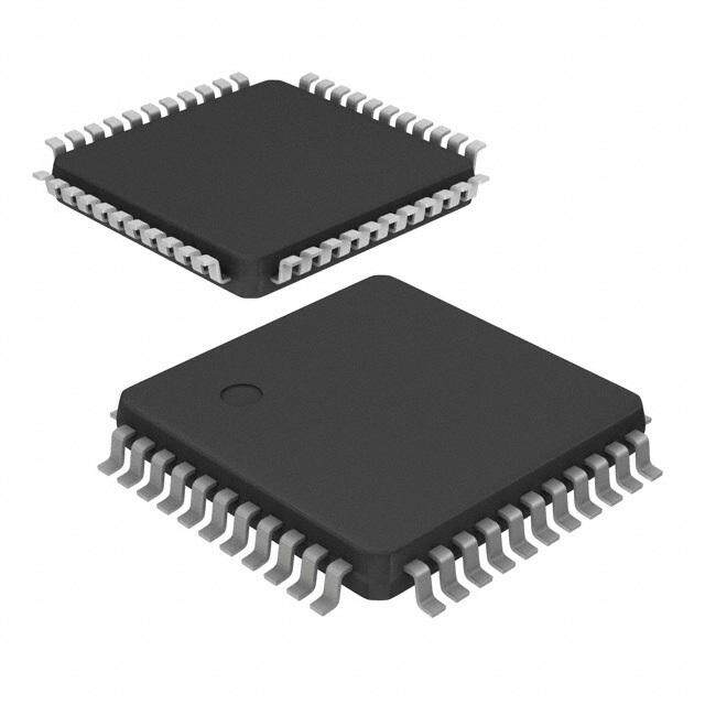
MSP430F5329,MSP430F5328,MSP430F5327 MSP430F5326,MSP430F5325,MSP430F5324 SLAS678F–AUGUST2010–REVISEDSEPTEMBER2019 www.ti.com The MSP430F5329, MSP430F5327, and MSP430F5325 are microcontroller configurations with an integrated 3.3-V LDO, four 16-bit timers, a high-performance 12-bit ADC, two USCIs, a hardware multiplier,DMA,anRTCmodulewithalarmcapabilities,and63I/Opins. The MSP430F5328, MSP430F5326, and MSP430F5324 include all of these peripherals but have 47 I/O pins. Typical applications include analog and digital sensor systems, data loggers, and various general-purpose applications. Forcompletemoduledescriptions,seethe MSP430F5xxandMSP430F6xxFamilyUser'sGuide. DeviceInformation(1) PARTNUMBER PACKAGE BODYSIZE(2) MSP430F5329IPN LQFP(80) 12mm×12mm MSP430F5328IZQE MicroStarJunior™BGA(80) 5mm×5mm MSP430F5328IRGC VQFN(64) 9mm×9mm (1) Forthemostcurrentpart,package,andorderinginformation,seethePackageOptionAddendumin Section8,orseetheTIwebsiteatwww.ti.com. (2) Thesizesshownhereareapproximations.Forthepackagedimensionswithtolerances,seethe MechanicalDatainSection8. 2 DeviceOverview Copyright©2010–2019,TexasInstrumentsIncorporated SubmitDocumentationFeedback ProductFolderLinks:MSP430F5329 MSP430F5328 MSP430F5327MSP430F5326 MSP430F5325 MSP430F5324
MSP430F5329,MSP430F5328,MSP430F5327 MSP430F5326,MSP430F5325,MSP430F5324 www.ti.com SLAS678F–AUGUST2010–REVISEDSEPTEMBER2019 1.4 Functional Block Diagrams Figure 1-1 shows the functional block diagram for the F5329, F5327, and F5325 devices in the PN package. XIN XOUTRST/NMI DVCC DVSS VCORE AVCC AVSS P1.x PPA2.x P3.x PPB4.x P5.x PPC6.x P7.x PPD8.x PU.0, LDOOLDOI PU.1 XT2IN SYS Unified ACLK Power I/O Ports I/O Ports I/O Ports I/O Ports XT2OUT SCylsotceMkmCLKSMCLK 196326428KKKKBBBB 864KKKBBB+++222KKKBBB MSBaVrnoLMawDg, enOSmoVueStnt WPCoa(ortPctn h4Mtrd)oaolpg an2IdnP× tW18eP, rA aIrP/ukO2pestup 2P×38P, BIP/O4s 2P×58P, C IP/O6s 11P××783P, D IIP//OO8ss PULD POort Flash RAM 1×16 I/Os 1×16 I/Os 1×16 I/Os 1×11 I/Os CPUXV2 MAB DMA and Working MDB 3 Channel Registers EEM (L: 8+2) USCI0,1 ADC12_A InJStTeBArfWGac,e MPY32 Ti5mT ACer0C_A Ti3mT ACer1C_A Ti3mT ACer2C_A Ti7mT BCer0C_B RTC_A CRC16 UIrSDUCAAI,R_ STAP,xI: 162 0C102h akBnsipntsels REF 12C COhMaPn_nBels Registers Registers Registers Registers USCI_Bx: (14 ext,2 int) SPI, I2C Autoscan Figure1-1.FunctionalBlockDiagram – MSP430F5329IPN,MSP430F5327IPN,MSP430F5325IPN Figure 1-2 shows the functional block diagram for the F5328, F5326, and F5324 devices in the ZQE or RGCpackage. XIN XOUTRST/NMI DVCC DVSS VCORE AVCC AVSS P1.x PPA2.x P3.x PPB4.x P5.x PPC6.x PU.0, LDOOLDOI PU.1 XT2IN SYS Unified ACLK Power I/O Ports I/O Ports I/O Ports XT2OUT SCylsotceMkmCLKSMCLK 196326428KKKKBBBB 864KKKBBB+++222KKKBBB MSBaVrnoLaMwDg/enSOmoVueStnt WPCoa(ortPctn h4Mtrd)oaolpg &2I nP×Wt18ePa, rA IkrP/ueO2pustp 11P××358P, BIIP//OO4ss 11P××568P, C IIP//OO6ss PULD POort Flash RAM 1×16 I/Os 1×13 I/Os 1×14 I/Os CPUXV2 MAB DMA and Working MDB 3 Channel Registers EEM (L: 8+2) USCI0,1 ADC12_A InJStTeBArfWGac,e MPY32 Ti5mT ACer0C_A Ti3mT ACer1C_A Ti3mT ACer2C_A Ti7mT BCer0C_B RTC_A CRC16 UIrSDUCAAI,R_ STAP,xI: 122 0C102h akBnsipntsels REF 8C COhManPn_eBls Registers Registers Registers Registers USCI_Bx: (10 ext,2 int) SPI, I2C Autoscan Figure1-2.FunctionalBlockDiagram – MSP430F5328IRGC,MSP430F5326IRGC,MSP430F5324IRGC, MSP430F5328IZQE,MSP430F5326IZQE,MSP430F5324IZQE Copyright©2010–2019,TexasInstrumentsIncorporated DeviceOverview 3 SubmitDocumentationFeedback ProductFolderLinks:MSP430F5329 MSP430F5328 MSP430F5327MSP430F5326 MSP430F5325 MSP430F5324
MSP430F5329,MSP430F5328,MSP430F5327 MSP430F5326,MSP430F5325,MSP430F5324 SLAS678F–AUGUST2010–REVISEDSEPTEMBER2019 www.ti.com Table of Contents 1 DeviceOverview......................................... 1 5.23 PMM,SVMHighSide............................... 30 .............................................. ................................ 1.1 Features 1 5.24 PMM,SVSLowSide 30 ........................................... ............................... 1.2 Applications 1 5.25 PMM,SVMLowSide 30 1.3 Description............................................ 1 5.26 Wake-upTimesFromLow-PowerModesand ................................................ ........................... Reset 31 1.4 FunctionalBlockDiagrams 3 ............................................. 2 Revision History......................................... 6 5.27 Timer_A 31 ............................................. 3 DeviceComparison ..................................... 8 5.28 Timer_B 31 .............. ..................................... 5.29 USCI(UARTMode)ClockFrequency 32 3.1 RelatedProducts 8 ................................. 4 TerminalConfigurationandFunctions.............. 9 5.30 USCI(UARTMode) 32 ......... ......................................... 5.31 USCI(SPIMasterMode)ClockFrequency 32 4.1 PinDiagrams 9 ............................ .................................. 5.32 USCI(SPIMasterMode) 32 4.2 SignalDescriptions 12 ............................. 5 Specifications........................................... 18 5.33 USCI(SPISlaveMode) 34 ........................ 5.34 USCI(I2CMode).................................... 36 5.1 AbsoluteMaximumRatings 18 ........................................ 5.35 12-BitADC,PowerSupplyandInputRange 5.2 ESDRatings 18 ........................................... Conditions 37 ............... 5.3 RecommendedOperatingConditions 18 .................... 5.36 12-BitADC,TimingParameters 37 5.4 ActiveModeSupplyCurrentIntoV Excluding ....................C.C................ 5.37 12-BitADC,LinearityParametersUsinganExternal External Current 19 ReferenceVoltageorAVCCasReferenceVoltage 38 5.5 Low-PowerModeSupplyCurrents(IntoV ) ................C.C......... 5.38 12-BitADC,LinearityParametersUsingtheInternal ExcludingExternalCurrent 20 .................................. Reference Voltage 38 ................ 5.6 ThermalResistanceCharacteristics 21 5.39 12-BitADC,TemperatureSensorandBuilt-InV 39 5.7 Schmitt-TriggerInputs–General-PurposeI/O MID ........................... (P1.0toP1.7,P2.0toP2.7,P3.0toP3.7,P4.0toP4.7) 5.40 REF,ExternalReference 40 (P5.0toP5.7,P6.0toP6.7,P7.0toP7.7,P8.0to 5.41 REF,Built-InReference............................. 41 ....................... P8.2,PJ.0toPJ.3,RST/NMI) 21 ....................................... 5.42 ComparatorB 42 5.8 Inputs–PortsP1andP2(P1.0toP1.7,P2.0to ................................ ................................................. 5.43 PortsPU.0andPU.1 42 P2.7) 21 ................... 5.44 LDO-PWR(LDOPowerSystem) 44 5.9 LeakageCurrent–General-PurposeI/O ....................................... (P1.0toP1.7,P2.0toP2.7,P3.0toP3.7,P4.0toP4.7) 5.45 FlashMemory 45 (P5.0toP5.7,P6.0toP6.7,P7.0toP7.7,P8.0to 5.46 JTAGandSpy-Bi-WireInterface.................... 45 ....................... P8.2,PJ.0toPJ.3,RST/NMI) 21 6 DetailedDescription................................... 46 5.10 Outputs–General-PurposeI/O(FullDriveStrength) ......................... 6.1 CPU(LinktoUser'sGuide) 46 (P1.0toP1.7,P2.0toP2.7,P3.0toP3.7,P4.0toP4.7) .................................... (P5.0toP5.7,P6.0toP6.7,P7.0toP7.7,P8.0to 6.2 OperatingModes 47 P8.2,PJ.0toPJ.3).................................. 22 6.3 InterruptVectorAddresses.......................... 48 5.11 Outputs–General-PurposeI/O(ReducedDrive ............................... 6.4 Memory Organization 49 Strength) .................................... (P1.0toP1.7,P2.0toP2.7,P3.0toP3.7,P4.0toP4.7) 6.5 Bootloader(BSL) 50 (P5.0toP5.7,P6.0toP6.7,P7.0toP7.7,P8.0to 6.6 JTAGOperation..................................... 50 .................................. P8.2,PJ.0toPJ.3) 22 ............... 6.7 FlashMemory(LinktoUser'sGuide) 51 5.12 OutputFrequency–General-PurposeI/O ......................... 6.8 RAM(LinktoUser'sGuide) 51 (P1.0toP1.7,P2.0toP2.7,P3.0toP3.7,P4.0toP4.7) .......................................... (P5.0toP5.7,P6.0toP6.7,P7.0toP7.7,P8.0to 6.9 Peripherals 51 P8.2,PJ.0toPJ.3).................................. 22 6.10 Input/OutputDiagrams.............................. 74 5.13 TypicalCharacteristics–Outputs,ReducedDrive 6.11 Device Descriptors.................................. 96 ............................... Strength(PxDS.y=0) 23 7 DeviceandDocumentationSupport............... 99 5.14 TypicalCharacteristics–Outputs,FullDrive ..................... ............................... 7.1 GettingStartedandNextSteps 99 Strength(PxDS.y=1) 24 ............................... ..... 7.2 Device Nomenclature 99 5.15 CrystalOscillator,XT1,Low-FrequencyMode 25 ................................ .............................. 7.3 ToolsandSoftware 101 5.16 CrystalOscillator,XT2 26 ............................ 7.4 DocumentationSupport 104 5.17 InternalVery-Low-PowerLow-FrequencyOscillator (VLO)................................................ 27 7.5 RelatedLinks...................................... 105 5.18 InternalReference,Low-FrequencyOscillator 7.6 CommunityResources............................. 106 (REFO).............................................. 27 7.7 Trademarks........................................ 106 5.19 DCO Frequency..................................... 28 7.8 ElectrostaticDischargeCaution................... 106 5.20 PMM,BrownoutReset(BOR)....................... 29 7.9 ExportControlNotice.............................. 106 5.21 PMM,CoreVoltage................................. 29 7.10 Glossary............................................ 106 ............................... 5.22 PMM,SVSHighSide 29 8 Mechanical,Packaging,andOrderable 4 TableofContents Copyright©2010–2019,TexasInstrumentsIncorporated SubmitDocumentationFeedback ProductFolderLinks:MSP430F5329 MSP430F5328 MSP430F5327MSP430F5326 MSP430F5325 MSP430F5324
MSP430F5329,MSP430F5328,MSP430F5327 MSP430F5326,MSP430F5325,MSP430F5324 www.ti.com SLAS678F–AUGUST2010–REVISEDSEPTEMBER2019 Information............................................. 107 Copyright©2010–2019,TexasInstrumentsIncorporated TableofContents 5 SubmitDocumentationFeedback ProductFolderLinks:MSP430F5329 MSP430F5328 MSP430F5327MSP430F5326 MSP430F5325 MSP430F5324
MSP430F5329,MSP430F5328,MSP430F5327 MSP430F5326,MSP430F5325,MSP430F5324 SLAS678F–AUGUST2010–REVISEDSEPTEMBER2019 www.ti.com 2 Revision History NOTE:Pagenumbersforpreviousrevisionsmaydifferfrompagenumbersinthecurrentversion. ChangesfromrevisionEtorevisionF ChangesfromSeptember26,2018toSeptember23,2019 Page • Addedthenote"TIrecommendsconnectingtheexposedthermalpadtoV "toFigure4-2,64-PinRGC SS Package(TopView)–MSP430F5328IRGC,MSP430F5326IRGC,MSP430F5324IRGC................................ 10 • AddedarowfortheQFNthermalpadtoTable4-1,SignalDescriptions................................................... 17 ChangesfromrevisionDtorevisionE ChangesfromFebruary27,2013toSeptember25,2018 Page • Changesthroughouttodocumentstructureandorganization,includingadditionofsectionnumbering ................. 1 • AddedSection1.2,Applications.................................................................................................... 1 • AddedDeviceInformationtable .................................................................................................... 2 • AddedSection1.4andmovedallfunctionalblockdiagramstoit.............................................................. 3 • AddedSection3.1,RelatedProducts.............................................................................................. 8 • AddedsignalnamestotheZQEpinout.......................................................................................... 11 • Added"PortUissuppliedbytheLDOOrail"tothePU.0andPU.1descriptionsinTable4-1,SignalDescriptions . 15 • AddednotetoRST/NMI/SBWTDIOpin.......................................................................................... 16 • AddedtypicalconditionsstatementsatthebeginningofSection5,Specifications........................................ 18 • AddedSection5,Specifications,andmovedallelectricalspecificationstoit .............................................. 18 • AddedSection5.2,ESDRatings.................................................................................................. 18 • AddednotetoC ............................................................................................................... 18 VCORE • MovedSection5.6,ThermalResistanceCharacteristics...................................................................... 21 • AddednotetoR .................................................................................................................. 21 Pull • ChangedtheTYPvalueoftheC parameterwithTestConditionsof"XTS=0,XCAPx=0"from2pFto1pF L,eff inSection5.15,CrystalOscillator,XT1,Low-FrequencyMode............................................................... 25 • ChangedtheMINvalueoftheV parameterfrom60mVto50mVinSection5.20,PMM,Brownout (DVCC_BOR_hys) Reset(BOR)......................................................................................................................... 29 • Updatednotes(1)and(2)andaddednote(3)inSection5.26,Wake-upTimesFromLow-PowerModesand Reset ................................................................................................................................. 31 • RemovedADC12DIVfromtheformulafortheTYPvalueinthesecondrowofthet parameterin CONVERT Section5.36,12-BitADC,TimingParameters,becauseADC12CLKisafterdivision..................................... 37 • Forthet parameterinSection5.42,Comparator_B:ChangedtheTestConditionofthefirstrowfrom EN_CMP "CBPWRMD=00,01,10"to"CBPWRMD=00,01";AddedasecondrowwithTestConditionsof"CBPWRMD =10"andMAXvalueof100µs................................................................................................... 42 • Changedallinstancesof"bootstraploader"to"bootloader"throughoutdocument........................................ 50 • CorrectedspellingofNMIIFGinTable6-8,SystemModuleInterruptVectorRegisters................................... 55 • ChangedTable6-56,PortPU.0,PU.1Functions............................................................................... 93 • AddedSection7,DeviceandDocumentationSupport,andmovedDeviceNomenclature,ESDCaution,and Trademarkssectionstoit .......................................................................................................... 99 • ReplacedformerToolsSupportsectionwithSection7.3,ToolsandSoftware........................................... 101 • AddedSection8,Mechanical,Packaging,andOrderableInformation..................................................... 107 6 RevisionHistory Copyright©2010–2019,TexasInstrumentsIncorporated SubmitDocumentationFeedback ProductFolderLinks:MSP430F5329 MSP430F5328 MSP430F5327MSP430F5326 MSP430F5325 MSP430F5324
MSP430F5329,MSP430F5328,MSP430F5327 MSP430F5326,MSP430F5325,MSP430F5324 www.ti.com SLAS678F–AUGUST2010–REVISEDSEPTEMBER2019 ChangesfrominitialreleasetorevisionD REVISION DESCRIPTION Table4-1,ChangedACLKdescription(addeddividersupto32) Table6-6,CorrectedtypoinPM_ANALOGnote Table6-8,ChangedSYSRSTIVinterrupteventat1ChtoReserved Section6.9.1,ChangeddescriptionofthenumberofI/Osineachportforthedifferentpackageoptions Section5.3,Addedtestconditionsfortypicalcharacteristics SLAS678D Section5.3,AddednoteregardinginteractionbetweenminimumVCCandSVS February2013 Section5.19,Addednote(1) Section5.37,ChangednoteregardingdecouplingcapacitorsonVREF+andVREF-pins Section5.39,Changedt MINvalueto100µs,Changednote(2) SENSOR(sample) Section5.45,ChangedvaluesofI andI ERASE MERASE Table 6-45, Table 6-46, Corrected notes regarding USCI CLK functions taking precedence over USCI STE functions SLAS678C AddedSection6.11 November2011 SLAS678B ProductionDatarelease October2011 SLAS678A UpdatedProductPreviewrelease August2011 SLAS678 ProductPreviewrelease August2010 Copyright©2010–2019,TexasInstrumentsIncorporated RevisionHistory 7 SubmitDocumentationFeedback ProductFolderLinks:MSP430F5329 MSP430F5328 MSP430F5327MSP430F5326 MSP430F5325 MSP430F5324
MSP430F5329,MSP430F5328,MSP430F5327 MSP430F5326,MSP430F5325,MSP430F5324 SLAS678F–AUGUST2010–REVISEDSEPTEMBER2019 www.ti.com 3 Device Comparison Table3-1summarizestheavailablefamilymembers. Table3-1.DeviceComparison(1)(2) USCI DEVICE FL(KABS)H S(RKABM) Timer_A(3) Timer_B(4) CUHAARNTN,EIrLDAA,: CHANNELB: AD(CC1h2)_A Co(mChp)_B I/O PACKAGE SPI,I2C SPI MSP430F5329 128 10 5,3,3 7 2 2 14ext,2int 12 63 80PN 64RGC, MSP430F5328 128 10 5,3,3 7 2 2 10ext,2int 8 47 80ZQE MSP430F5327 96 8 5,3,3 7 2 2 14ext,2int 12 63 80PN 64RGC, MSP430F5326 96 8 5,3,3 7 2 2 10ext,2int 8 47 80ZQE MSP430F5325 64 6 5,3,3 7 2 2 14ext,2int 12 63 80PN 64RGC, MSP430F5324 64 6 5,3,3 7 2 2 10ext,2int 8 47 80ZQE (1) Forthemostcurrentpackageandorderinginformation,seethePackageOptionAddenduminSection8,orseetheTIwebsiteat www.ti.com. (2) Packagedrawings,standardpackingquantities,thermaldata,symbolization,andPCBdesignguidelinesareavailableat www.ti.com/packaging. (3) EachnumberinthesequencerepresentsaninstantiationofTimer_AwithitsassociatednumberofcapturecompareregistersandPWM outputgeneratorsavailable.Forexample,anumbersequenceof3,5wouldrepresenttwoinstantiationsofTimer_A,thefirst instantiationhaving3andthesecondinstantiationhaving5capturecompareregistersandPWMoutputgenerators,respectively. (4) EachnumberinthesequencerepresentsaninstantiationofTimer_BwithitsassociatednumberofcapturecompareregistersandPWM outputgeneratorsavailable.Forexample,anumbersequenceof3,5wouldrepresenttwoinstantiationsofTimer_B,thefirst instantiationhaving3andthesecondinstantiationhaving5capturecompareregistersandPWMoutputgenerators,respectively. 3.1 Related Products Forinformationaboutotherdevicesinthisfamilyofproductsorrelatedproducts,seethefollowinglinks. ProductsforTImicrocontrollers TI's low-power and high-performance MCUs, with wired and wireless connectivity options, are optimizedforabroadrangeofapplications. ProductsforMSP430ultra-low-powermicrocontrollers Oneplatform.Oneecosystem.Endlesspossibilities. CompanionproductsforMSP430F5329 Reviewproductsthatarefrequentlypurchasedorusedinconjunctionwiththisproduct. Referencedesigns Find reference designs leveraging the best in TI technology – from analog and power management to embeddedprocessors. 8 DeviceComparison Copyright©2010–2019,TexasInstrumentsIncorporated SubmitDocumentationFeedback ProductFolderLinks:MSP430F5329 MSP430F5328 MSP430F5327MSP430F5326 MSP430F5325 MSP430F5324
MSP430F5329,MSP430F5328,MSP430F5327 MSP430F5326,MSP430F5325,MSP430F5324 www.ti.com SLAS678F–AUGUST2010–REVISEDSEPTEMBER2019 4 Terminal Configuration and Functions 4.1 Pin Diagrams Figure4-1showsthepinoutfortheF5329,F5327,andF5325devicesinthe80-pinPNpackage. O DI T K P6.3/CB3/A3P6.2/CB2/A2P6.1/CB1/A1P6.0/CB0/A0RST/NMI/SBWPJ.3/TCKPJ.2/TMSPJ.1/TDI/TCLKPJ.0/TDOTEST/SBWTCP5.3/XT2OUTP5.2/XT2INAVSS2NCLDOOLDOIPU.1NCPU.0USSV 09876543210987654321 87777777777666666666 P6.4/CB4/A4 1 60 P7.7/TB0CLK/MCLK P6.5/CB5/A5 2 59 P7.6/TB0.4 P6.6/CB6/A6 3 58 P7.5/TB0.3 P6.7/CB7/A7 4 57 P7.4/TB0.2 P7.0/CB8/A12 5 56 P5.7/TB0.1 P7.1/CB9/A13 6 55 P5.6/TB0.0 P7.2/CB10/A14 7 54 P4.7/PM_NONE P7.3/CB11/A15 8 53 P4.6/PM_NONE P5.0/A8/VREF+/VeREF+ 9 52 P4.5/PM_UCA1RXD/PM_UCA1SOMI P5.1/A9/VREF−/VeREF− 10 MSP430F5329IPN 51 P4.4/PM_UCA1TXD/PM_UCA1SIMO MSP430F5327IPN AVCC1 11 50 DVCC2 MSP430F5325IPN P5.4/XIN 12 49 DVSS2 P5.5/XOUT 13 48 P4.3/PM_UCB1CLK/PM_UCA1STE AVSS1 14 47 P4.2/PM_UCB1SOMI/PM_UCB1SCL P8.0 15 46 P4.1/PM_UCB1SIMO/PM_UCB1SDA P8.1 16 45 P4.0/PM_UCB1STE/PM_UCA1CLK P8.2 17 44 P3.7/TB0OUTH/SVMOUT DVCC1 18 43 P3.6/TB0.6 DVSS1 19 42 P3.5/TB0.5 VCORE 20 41 P3.4/UCA0RXD/UCA0SOMI 12345678901234567890 22222222233333333334 0/TA0CLK/ACLKP1.1/TA0.0P1.2/TA0.1P1.3/TA0.2P1.4/TA0.3P1.5/TA0.4TA1CLK/CBOUTP1.7/TA1.0P2.0/TA1.1P2.1/TA1.2TA2CLK/SMCLKP2.3/TA2.0P2.4/TA2.1P2.5/TA2.2RTCCLK/DMAE00STE/UCA0CLKSIMO/UCB0SDASOMI/UCB0SCL0CLK/UCA0STETXD/UCA0SIMO P1. P1.6/ P2.2/ P2.6/P2.7/UCB3.0/UCB03.1/UCB0P3.2/UCB3.3/UCA0 PP P Figure4-1.80-PinPNPackage(TopView) – MSP430F5329IPN,MSP430F5327IPN,MSP430F5325IPN Copyright©2010–2019,TexasInstrumentsIncorporated TerminalConfigurationandFunctions 9 SubmitDocumentationFeedback ProductFolderLinks:MSP430F5329 MSP430F5328 MSP430F5327MSP430F5326 MSP430F5325 MSP430F5324
MSP430F5329,MSP430F5328,MSP430F5327 MSP430F5326,MSP430F5325,MSP430F5324 SLAS678F–AUGUST2010–REVISEDSEPTEMBER2019 www.ti.com Figure4-2showsthepinoutfortheF5328,F5326,andF5324devicesinthe64-pinRGCpackage. O DI T K RST/NMI/SBW PJ.3/TCK PJ.2/TMS PJ.1/TDI/TCLK PJ.0/TDO TEST/SBWTC P5.3/XT2OUT P5.2/XT2IN AVSS2 NC LDOO LDOI PU.1 NC PU.0 USSV 64 63 62 6160 59 58 57 56 55 54 53 52 5150 49 P6.0/CB0/A0 1 48 P4.7/PM_NONE P6.1/CB1/A1 2 47 P4.6/PM_NONE P6.2/CB2/A2 3 46 P4.5/PM_UCA1RXD/PM_UCA1SOMI P6.3/CB3/A3 4 45 P4.4/PM_UCA1TXD/PM_UCA1SIMO P6.4/CB4/A4 5 44 P4.3/PM_UCB1CLK/PM_UCA1STE P6.5/CB5/A5 6 43 P4.2/PM_UCB1SOMI/PM_UCB1SCL P6.6/CB6/A6 7 42 P4.1/PM_UCB1SIMO/PM_UCB1SDA MSP430F5328IRGC P6.7/CB7/A7 8 41 P4.0/PM_UCB1STE/PM_UCA1CLK MSP430F5326IRGC P5.0/A8/VREF+/VeREF+ 9 MSP430F5324IRGC 40 DVCC2 P5.1/A9/VREF−/VeREF− 10 39 DVSS2 AVCC1 11 38 P3.4/UCA0RXD/UCA0SOMI P5.4/XIN 12 37 P3.3/UCA0TXD/UCA0SIMO P5.5/XOUT 13 36 P3.2/UCB0CLK/UCA0STE AVSS1 14 35 P3.1/UCB0SOMI/UCB0SCL DVCC1 15 34 P3.0/UCB0SIMO/UCB0SDA DVSS1 16 33 P2.7/UCB0STE/UCA0CLK 17 18 19 20 212223 24 25 26 27 28 29 30 3132 RE LK 0.0 0.1 0.2 0.3 0.4 UT 1.0 1.1 1.2 LK 2.0 2.1 2.2 E0 O C A A A A A O A A A C A A A A VC CLK/A P1.1/T P1.2/T P1.3/T P1.4/T P1.5/T LK/CB P1.7/T P2.0/T P2.1/T LK/SM P2.3/T P2.4/T P2.5/T LK/DM 0 C C C 0/TA TA1 TA2 RTC P1. P1.6/ P2.2/ P2.6/ NOTE: TIrecommendsconnectingtheexposedthermalpadtoV . SS Figure4-2.64-PinRGCPackage(TopView) – MSP430F5328IRGC,MSP430F5326IRGC, MSP430F5324IRGC 10 TerminalConfigurationandFunctions Copyright©2010–2019,TexasInstrumentsIncorporated SubmitDocumentationFeedback ProductFolderLinks:MSP430F5329 MSP430F5328 MSP430F5327MSP430F5326 MSP430F5325 MSP430F5324
MSP430F5329,MSP430F5328,MSP430F5327 MSP430F5326,MSP430F5325,MSP430F5324 www.ti.com SLAS678F–AUGUST2010–REVISEDSEPTEMBER2019 Figure 4-3 shows the pinout for the F5328, F5326, and F5324 devices in the 80-pin ZQE package. This figureshowsthedefaultsignalnameforeachpin;seeTable4-1foradditionalsignals. P6.0 RST PJ.2 TEST AVSS2 LDOO LDOI PU.1 PU.0 A1 A2 A3 A4 A5 A6 A7 A8 A9 P6.2 P6.1 PJ.3 P5.3 P5.2 NC NC VSSU VSSU B1 B2 B3 B4 B5 B6 B7 B8 B9 P6.4 P6.3 PJ.1 PJ.0 Reserved P4.7 P4.6 P4.5 C1 C2 C4 C5 C6 C7 C8 C9 P6.6 P6.5 P6.7 ReservedReservedReserved P4.4 P4.3 P4.2 D1 D2 D3 D4 D5 D6 D7 D8 D9 P5.0 P5.1 ReservedReservedReservedReserved P4.1 P4.0 DVCC2 E1 E2 E3 E4 E5 E6 E7 E8 E9 P5.4 AVCC1 ReservedReservedReservedReservedReservedReserved DVSS2 F1 F2 F3 F4 F5 F6 F7 F8 F9 P5.5 AVSS1Reserved P1.3 P1.6 P2.1 P3.4 P3.2 P3.3 G1 G2 G3 G4 G5 G6 G7 G8 G9 DVCC1 P1.0 P1.1 P1.4 P1.7 P2.3 P2.7 P3.0 P3.1 H1 H2 H3 H4 H5 H6 H7 H8 H9 DVSS1 VCORE P1.2 P1.5 P2.0 P2.2 P2.4 P2.5 P2.6 J1 J2 J3 J4 J5 J6 J7 J8 J9 Figure4-3.80-PinZQEPackage(TopView) –MSP430F5328IZQE,MSP430F5326IZQE,MSP430F5324IZQE Copyright©2010–2019,TexasInstrumentsIncorporated TerminalConfigurationandFunctions 11 SubmitDocumentationFeedback ProductFolderLinks:MSP430F5329 MSP430F5328 MSP430F5327MSP430F5326 MSP430F5325 MSP430F5324
MSP430F5329,MSP430F5328,MSP430F5327 MSP430F5326,MSP430F5325,MSP430F5324 SLAS678F–AUGUST2010–REVISEDSEPTEMBER2019 www.ti.com 4.2 Signal Descriptions Table4-1describesthesignalsforalldevicevariantsandpackageoptions. Table4-1.SignalDescriptions TERMINAL NO. I/O(1) DESCRIPTION NAME PN RGC ZQE General-purposedigitalI/O P6.4/CB4/A4 1 5 C1 I/O Comparator_BinputCB4 AnaloginputA4forADC General-purposedigitalI/O P6.5/CB5/A5 2 6 D2 I/O Comparator_BinputCB5 AnaloginputA5forADC General-purposedigitalI/O P6.6/CB6/A6 3 7 D1 I/O Comparator_BinputCB6 AnaloginputA6forADC General-purposedigitalI/O P6.7/CB7/A7 4 8 D3 I/O Comparator_BinputCB7 AnaloginputA7forADC General-purposedigitalI/O(notavailableonF5328,F5326,F5324devices) P7.0/CB8/A12 5 N/A N/A I/O Comparator_BinputCB8(notavailableonF5328,F5326,F5324devices) AnaloginputA12forADC(notavailableonF5328,F5326,F5324devices) General-purposedigitalI/O(notavailableonF5328,F5326,F5324devices) P7.1/CB9/A13 6 N/A N/A I/O Comparator_BinputCB9(notavailableonF5328,F5326,F5324devices) AnaloginputA13forADC(notavailableonF5328,F5326,F5324devices) General-purposedigitalI/O(notavailableonF5328,F5326,F5324devices) Comparator_BinputCB10(notavailableonF5328,F5326,F5324 P7.2/CB10/A14 7 N/A N/A I/O devices) AnaloginputA14forADC(notavailableonF5328,F5326,F5324devices) General-purposedigitalI/O(notavailableonF5328,F5326,F5324devices) P7.3/CB11/A15 8 N/A N/A I/O Comparator_BinputCB11(notavailableonF5328,F5326,F5324devices) AnaloginputA15forADC(notavailableonF5328,F5326,F5324devices) General-purposedigitalI/O AnaloginputA8forADC P5.0/A8/VREF+/VeREF+ 9 9 E1 I/O OutputofreferencevoltagetotheADC InputforanexternalreferencevoltagetotheADC General-purposedigitalI/O AnaloginputA9forADC P5.1/A9/VREF-/VeREF- 10 10 E2 I/O NegativeterminalfortheADCreferencevoltageforbothsources,theinternal referencevoltage,oranexternalappliedreferencevoltage AVCC1 11 11 F2 Analogpowersupply General-purposedigitalI/O P5.4/XIN 12 12 F1 I/O InputterminalforcrystaloscillatorXT1 General-purposedigitalI/O P5.5/XOUT 13 13 G1 I/O OutputterminalofcrystaloscillatorXT1 (1) I=input,O=output,N/A=notavailable 12 TerminalConfigurationandFunctions Copyright©2010–2019,TexasInstrumentsIncorporated SubmitDocumentationFeedback ProductFolderLinks:MSP430F5329 MSP430F5328 MSP430F5327MSP430F5326 MSP430F5325 MSP430F5324
MSP430F5329,MSP430F5328,MSP430F5327 MSP430F5326,MSP430F5325,MSP430F5324 www.ti.com SLAS678F–AUGUST2010–REVISEDSEPTEMBER2019 Table4-1.SignalDescriptions(continued) TERMINAL NO. I/O(1) DESCRIPTION NAME PN RGC ZQE AVSS1 14 14 G2 Analoggroundsupply P8.0 15 N/A N/A I/O General-purposedigitalI/O P8.1 16 N/A N/A I/O General-purposedigitalI/O P8.2 17 N/A N/A I/O General-purposedigitalI/O DVCC1 18 15 H1 Digitalpowersupply DVSS1 19 16 J1 Digitalgroundsupply VCORE(2) 20 17 J2 Regulatedcorepowersupplyoutput(internaluseonly,noexternalcurrent loading) General-purposedigitalI/Owithportinterrupt P1.0/TA0CLK/ACLK 21 18 H2 I/O TA0clocksignalTA0CLKinput ACLKoutput(dividedby1,2,4,8,16,or32) General-purposedigitalI/Owithportinterrupt P1.1/TA0.0 22 19 H3 I/O TA0CCR0capture:CCI0Ainput,compare:Out0output BSLtransmitoutput General-purposedigitalI/Owithportinterrupt P1.2/TA0.1 23 20 J3 I/O TA0CCR1capture:CCI1Ainput,compare:Out1output BSLreceiveinput General-purposedigitalI/Owithportinterrupt P1.3/TA0.2 24 21 G4 I/O TA0CCR2capture:CCI2Ainput,compare:Out2output General-purposedigitalI/Owithportinterrupt P1.4/TA0.3 25 22 H4 I/O TA0CCR3capture:CCI3Ainputcompare:Out3output General-purposedigitalI/Owithportinterrupt P1.5/TA0.4 26 23 J4 I/O TA0CCR4capture:CCI4Ainput,compare:Out4output General-purposedigitalI/Owithportinterrupt P1.6/TA1CLK/CBOUT 27 24 G5 I/O TA1clocksignalTA1CLKinput Comparator_Boutput General-purposedigitalI/Owithportinterrupt P1.7/TA1.0 28 25 H5 I/O TA1CCR0capture:CCI0Ainput,compare:Out0output General-purposedigitalI/Owithportinterrupt P2.0/TA1.1 29 26 J5 I/O TA1CCR1capture:CCI1Ainput,compare:Out1output General-purposedigitalI/Owithportinterrupt P2.1/TA1.2 30 27 G6 I/O TA1CCR2capture:CCI2Ainput,compare:Out2output General-purposedigitalI/Owithportinterrupt P2.2/TA2CLK/SMCLK 31 28 J6 I/O TA2clocksignalTA2CLKinput;SMCLKoutput General-purposedigitalI/Owithportinterrupt P2.3/TA2.0 32 29 H6 I/O TA2CCR0capture:CCI0Ainput,compare:Out0output General-purposedigitalI/Owithportinterrupt P2.4/TA2.1 33 30 J7 I/O TA2CCR1capture:CCI1Ainput,compare:Out1output General-purposedigitalI/Owithportinterrupt P2.5/TA2.2 34 31 J8 I/O TA2CCR2capture:CCI2Ainput,compare:Out2output (2) VCOREisforinternaluseonly.Noexternalcurrentloadingispossible.VCOREshouldbeconnectedonlytotherecommended capacitorvalue,C . VCORE Copyright©2010–2019,TexasInstrumentsIncorporated TerminalConfigurationandFunctions 13 SubmitDocumentationFeedback ProductFolderLinks:MSP430F5329 MSP430F5328 MSP430F5327MSP430F5326 MSP430F5325 MSP430F5324
MSP430F5329,MSP430F5328,MSP430F5327 MSP430F5326,MSP430F5325,MSP430F5324 SLAS678F–AUGUST2010–REVISEDSEPTEMBER2019 www.ti.com Table4-1.SignalDescriptions(continued) TERMINAL NO. I/O(1) DESCRIPTION NAME PN RGC ZQE General-purposedigitalI/Owithportinterrupt P2.6/RTCCLK/DMAE0 35 32 J9 I/O RTCclockoutputforcalibration DMAexternaltriggerinput General-purposedigitalI/Owithportinterrupt P2.7/UCB0STE/ Slavetransmitenable–USCI_B0SPImode 36 33 H7 I/O UCA0CLK Clocksignalinput–USCI_A0SPIslavemode Clocksignaloutput–USCI_A0SPImastermode General-purposedigitalI/O P3.0/UCB0SIMO/ 37 34 H8 I/O Slavein,masterout–USCI_B0SPImode UCB0SDA I2Cdata–USCI_B0I2Cmode General-purposedigitalI/O P3.1/UCB0SOMI/ 38 35 H9 I/O Slaveout,masterin–USCI_B0SPImode UCB0SCL I2Cclock–USCI_B0I2Cmode General-purposedigitalI/O P3.2/UCB0CLK/ Clocksignalinput–USCI_B0SPIslavemode 39 36 G8 I/O UCA0STE Clocksignaloutput–USCI_B0SPImastermode Slavetransmitenable–USCI_A0SPImode General-purposedigitalI/O P3.3/UCA0TXD/ 40 37 G9 I/O Transmitdata–USCI_A0UARTmode UCA0SIMO Slavein,masterout–USCI_A0SPImode General-purposedigitalI/O P3.4/UCA0RXD/ 41 38 G7 I/O Receivedata–USCI_A0UARTmode UCA0SOMI Slaveout,masterin–USCI_A0SPImode General-purposedigitalI/O(notavailableonF5328,F5326,F5324devices) P3.5/TB0.5 42 N/A N/A I/O TB0CCR5capture:CCI5Ainput,compare:Out5output General-purposedigitalI/O(notavailableonF5328,F5326,F5324devices) P3.6/TB0.6 43 N/A N/A I/O TB0CCR6capture:CCI6Ainput,compare:Out6output General-purposedigitalI/O(notavailableonF5328,F5326,F5324devices) P3.7/TB0OUTH/ SwitchallPWMoutputshigh-impedanceinput–TB0(notavailableonF5328, 44 N/A N/A I/O SVMOUT F5326,F5324devices) SVMoutput(notavailableonF5328,F5326,F5324devices) General-purposedigitalI/Owithreconfigurableportmappingsecondary function P4.0/PM_UCB1STE/ 45 41 E8 I/O Defaultmapping:Slavetransmitenable–USCI_B1SPImode PM_UCA1CLK Defaultmapping:Clocksignalinput–USCI_A1SPIslavemode Defaultmapping:Clocksignaloutput–USCI_A1SPImastermode General-purposedigitalI/Owithreconfigurableportmappingsecondary function P4.1/PM_UCB1SIMO/ 46 42 E7 I/O PM_UCB1SDA Defaultmapping:Slavein,masterout–USCI_B1SPImode Defaultmapping:I2Cdata–USCI_B1I2Cmode 14 TerminalConfigurationandFunctions Copyright©2010–2019,TexasInstrumentsIncorporated SubmitDocumentationFeedback ProductFolderLinks:MSP430F5329 MSP430F5328 MSP430F5327MSP430F5326 MSP430F5325 MSP430F5324
MSP430F5329,MSP430F5328,MSP430F5327 MSP430F5326,MSP430F5325,MSP430F5324 www.ti.com SLAS678F–AUGUST2010–REVISEDSEPTEMBER2019 Table4-1.SignalDescriptions(continued) TERMINAL NO. I/O(1) DESCRIPTION NAME PN RGC ZQE General-purposedigitalI/Owithreconfigurableportmappingsecondary function P4.2/PM_UCB1SOMI/ 47 43 D9 I/O PM_UCB1SCL Defaultmapping:Slaveout,masterin–USCI_B1SPImode Defaultmapping:I2Cclock–USCI_B1I2Cmode General-purposedigitalI/Owithreconfigurableportmappingsecondary function P4.3/PM_UCB1CLK/ 48 44 D8 I/O Defaultmapping:Clocksignalinput–USCI_B1SPIslavemode PM_UCA1STE Defaultmapping:Clocksignaloutput–USCI_B1SPImastermode Defaultmapping:Slavetransmitenable–USCI_A1SPImode DVSS2 49 39 F9 Digitalgroundsupply DVCC2 50 40 E9 Digitalpowersupply General-purposedigitalI/Owithreconfigurableportmappingsecondary function P4.4/PM_UCA1TXD/ 51 45 D7 I/O PM_UCA1SIMO Defaultmapping:Transmitdata–USCI_A1UARTmode Defaultmapping:Slavein,masterout–USCI_A1SPImode General-purposedigitalI/Owithreconfigurableportmappingsecondary function P4.5/PM_UCA1RXD/ 52 46 C9 I/O PM_UCA1SOMI Defaultmapping:Receivedata–USCI_A1UARTmode Defaultmapping:Slaveout,masterin–USCI_A1SPImode General-purposedigitalI/Owithreconfigurableportmappingsecondary P4.6/PM_NONE 53 47 C8 I/O function Defaultmapping:nosecondaryfunction. General-purposedigitalI/Owithreconfigurableportmappingsecondary P4.7/PM_NONE 54 48 C7 I/O function Defaultmapping:nosecondaryfunction. General-purposedigitalI/O(notavailableonF5328,F5326,F5324devices) P5.6/TB0.0 55 N/A N/A I/O TB0 CCR0 capture: CCI0A input, compare: Out0 output (not available on F5328,F5326,F5324devices) General-purposedigitalI/O(notavailableonF5328,F5326,F5324devices) P5.7/TB0.1 56 N/A N/A I/O TB0 CCR1 capture: CCI1A input, compare: Out1 output (not available on F5328,F5326,F5324devices) General-purposedigitalI/O(notavailableonF5328,F5326,F5324devices) P7.4/TB0.2 57 N/A N/A I/O TB0 CCR2 capture: CCI2A input, compare: Out2 output (not available on F5328,F5326,F5324devices) General-purposedigitalI/O(notavailableonF5328,F5326,F5324devices) P7.5/TB0.3 58 N/A N/A I/O TB0 CCR3 capture: CCI3A input, compare: Out3 output (not available on F5328,F5326,F5324devices) General-purposedigitalI/O(notavailableonF5328,F5326,F5324devices) P7.6/TB0.4 59 N/A N/A I/O TB0 CCR4 capture: CCI4A input, compare: Out4 output (not available on F5328,F5326,F5324devices) General-purposedigitalI/O(notavailableonF5328,F5326,F5324devices) TB0 clock signal TBCLK input (not available on F5328, F5326, F5324 P7.7/TB0CLK/MCLK 60 N/A N/A I/O devices) MCLKoutput(notavailableonF5328,F5326,F5324devices) VSSU 61 49 B8,B9 PortUgroundsupply General-purposedigitalI/O,controlledbyPUcontrolregister,PortUis PU.0 62 50 A9 I/O suppliedbytheLDOOrail Copyright©2010–2019,TexasInstrumentsIncorporated TerminalConfigurationandFunctions 15 SubmitDocumentationFeedback ProductFolderLinks:MSP430F5329 MSP430F5328 MSP430F5327MSP430F5326 MSP430F5325 MSP430F5324
MSP430F5329,MSP430F5328,MSP430F5327 MSP430F5326,MSP430F5325,MSP430F5324 SLAS678F–AUGUST2010–REVISEDSEPTEMBER2019 www.ti.com Table4-1.SignalDescriptions(continued) TERMINAL NO. I/O(1) DESCRIPTION NAME PN RGC ZQE NC 63 51 B7 I/O Noconnect General-purposedigitalI/O,controlledbyPUcontrolregister,PortUis PU.1 64 52 A8 I/O suppliedbytheLDOOrail LDOI 65 53 A7 LDOinput LDOO 66 54 A6 LDOoutput NC 67 55 B6 Noconnect AVSS2 68 56 A5 Analoggroundsupply General-purposedigitalI/O P5.2/XT2IN 69 57 B5 I/O InputterminalforcrystaloscillatorXT2 General-purposedigitalI/O P5.3/XT2OUT 70 58 B4 I/O OutputterminalofcrystaloscillatorXT2 Testmodepin–SelectsfourwireJTAGoperation. TEST/SBWTCK(3) 71 59 A4 I Spy-Bi-WireinputclockwhenSpy-Bi-Wireoperationactivated General-purposedigitalI/O PJ.0/TDO(4) 72 60 C5 I/O JTAGtestdataoutputport General-purposedigitalI/O PJ.1/TDI/TCLK(4) 73 61 C4 I/O JTAGtestdatainputortestclockinput General-purposedigitalI/O PJ.2/TMS(4) 74 62 A3 I/O JTAGtestmodeselect General-purposedigitalI/O PJ.3/TCK(4) 75 63 B3 I/O JTAGtestclock Resetinputactivelow(5) RST/NMI/SBWTDIO(3) 76 64 A2 I/O Nonmaskableinterruptinput Spy-Bi-Wiredatainput/outputwhenSpy-Bi-Wireoperationactivated. General-purposedigitalI/O P6.0/CB0/A0 77 1 A1 I/O Comparator_BinputCB0 AnaloginputA0forADC General-purposedigitalI/O P6.1/CB1/A1 78 2 B2 I/O Comparator_BinputCB1 AnaloginputA1forADC General-purposedigitalI/O P6.2/CB2/A2 79 3 B1 I/O Comparator_BinputCB2 AnaloginputA2forADC General-purposedigitalI/O P6.3/CB3/A3 80 4 C2 I/O Comparator_BinputCB3 AnaloginputA3forADC (3) SeeSection6.5andSection6.6forusewithBSLandJTAGfunctions,respectively. (4) SeeSection6.6forusewithJTAGfunction. (5) Whenthispinisconfiguredasreset,theinternalpullupresistorisenabledbydefault. 16 TerminalConfigurationandFunctions Copyright©2010–2019,TexasInstrumentsIncorporated SubmitDocumentationFeedback ProductFolderLinks:MSP430F5329 MSP430F5328 MSP430F5327MSP430F5326 MSP430F5325 MSP430F5324
MSP430F5329,MSP430F5328,MSP430F5327 MSP430F5326,MSP430F5325,MSP430F5324 www.ti.com SLAS678F–AUGUST2010–REVISEDSEPTEMBER2019 Table4-1.SignalDescriptions(continued) TERMINAL NO. I/O(1) DESCRIPTION NAME PN RGC ZQE C6, D4, D5, D6, E3, E4, E5, Reserved N/A N/A E6, Reserved.Connecttoground. F3, F4, F5, F6, F7, F8, G3 Thepackagethermalpadmustbesolderedtotheprintedcircuitboardfor Thermalpad – Pad – thermalandmechanicalperformance.TIrecommendsconnectiontoV . SS Copyright©2010–2019,TexasInstrumentsIncorporated TerminalConfigurationandFunctions 17 SubmitDocumentationFeedback ProductFolderLinks:MSP430F5329 MSP430F5328 MSP430F5327MSP430F5326 MSP430F5325 MSP430F5324
MSP430F5329,MSP430F5328,MSP430F5327 MSP430F5326,MSP430F5325,MSP430F5324 SLAS678F–AUGUST2010–REVISEDSEPTEMBER2019 www.ti.com 5 Specifications Allgraphsinthissectionarefortypicalconditions,unlessotherwisenoted. Typical(TYP)valuesarespecifiedatV =3.3VandT =25°C,unlessotherwisenoted. CC A 5.1 Absolute Maximum Ratings(1) overoperatingfree-airtemperaturerange(unlessotherwisenoted) MIN MAX UNIT VoltageappliedatV toV –0.3 4.1 V CC SS Voltageappliedtoanypin(excludingVCORE,LDOI)(2) –0.3 V +0.3 V CC Diodecurrentatanydevicepin ±2 mA Storagetemperature,T (3) –55 150 °C stg (1) StressesbeyondthoselistedunderAbsoluteMaximumRatingsmaycausepermanentdamagetothedevice.Thesearestressratings only,andfunctionaloperationofthedeviceattheseoranyotherconditionsbeyondthoseindicatedunderRecommendedOperating Conditionsisnotimplied.Exposuretoabsolute-maximum-ratedconditionsforextendedperiodsmayaffectdevicereliability. (2) AllvoltagesreferencedtoV .VCOREisforinternaldeviceuseonly.NoexternalDCloadingorvoltageshouldbeapplied. SS (3) HighertemperaturemaybeappliedduringboardsolderingaccordingtothecurrentJEDECJ-STD-020specificationwithpeakreflow temperaturesnothigherthanclassifiedonthedevicelabelontheshippingboxesorreels. 5.2 ESD Ratings VALUE UNIT Human-bodymodel(HBM),perANSI/ESDA/JEDECJS-001(1) ±1000 V Electrostaticdischarge V (ESD) Charged-devicemodel(CDM),perJEDECspecificationJESD22-C101(2) ±250 (1) JEDECdocumentJEP155statesthat500-VHBMallowssafemanufacturingwithastandardESDcontrolprocess.Manufacturingwith lessthan500-VHBMispossiblewiththenecessaryprecautions.Pinslistedas±1000Vmayactuallyhavehigherperformance. (2) JEDECdocumentJEP157statesthat250-VCDMallowssafemanufacturingwithastandardESDcontrolprocess.Manufacturingwith lessthan250-VCDMispossiblewiththenecessaryprecautions.Pinslistedas±250Vmayactuallyhavehigherperformance. 5.3 Recommended Operating Conditions MIN NOM MAX UNIT PMMCOREVx=0 1.8 3.6 Supplyvoltageduringprogramexecutionandflash PMMCOREVx=0,1 2.0 3.6 VCC programming(AVCCx=DVCCx =VCC)(1)(2) PMMCOREVx=0,1,2 2.2 3.6 V PMMCOREVx=0,1,2,3 2.4 3.6 V Supplyvoltage(AVSSx =DVSSx =V ) 0 V SS SS T Operatingfree-airtemperature –40 85 °C A T Operatingjunctiontemperature –40 85 °C J C RecommendedcapacitoratVCORE(3) 470 nF VCORE C / DVCC CapacitorratioofDVCCtoVCORE 10 C VCORE PMMCOREVx=0, 1.8V≤V ≤3.6V 0 8.0 CC (defaultcondition) PMMCOREVx=1, fSYSTEM P(sreoeceFsigsourrefr5e-q1u)ency(maximumMCLKfrequency)(4) 2.0V≤VCC≤3.6V 0 12.0 MHz PMMCOREVx=2, 0 20.0 2.2V≤V ≤3.6V CC PMMCOREVx=3, 0 25.0 2.4V≤V ≤3.6V CC (1) TIrecommendspoweringAVCCandDVCCfromthesamesource.Amaximumdifferenceof0.3VbetweenAVCCandDVCCcanbe toleratedduringpowerupandoperation. (2) TheminimumsupplyvoltageisdefinedbythesupervisorSVSlevelswhenitisenabled.SeethethresholdparametersinSection5.22 fortheexactvaluesandfurtherdetails. (3) Acapacitortoleranceof±20%orbetterisrequired. (4) Modulesmayhaveadifferentmaximuminputclockspecification.Seethespecificationoftherespectivemoduleinthisdatasheet. 18 Specifications Copyright©2010–2019,TexasInstrumentsIncorporated SubmitDocumentationFeedback ProductFolderLinks:MSP430F5329 MSP430F5328 MSP430F5327MSP430F5326 MSP430F5325 MSP430F5324
MSP430F5329,MSP430F5328,MSP430F5327 MSP430F5326,MSP430F5325,MSP430F5324 www.ti.com SLAS678F–AUGUST2010–REVISEDSEPTEMBER2019 25 3 20 z H M 2 2, 3 y - c n 12 e u q e 1 1, 2 1, 2, 3 Fr m 8 e st y S 0 0, 1 0, 1, 2 0, 1, 2, 3 0 1.8 2.0 2.2 2.4 3.6 Supply Voltage - V NOTE:The numbers within the fields denote the supported PMMCOREVx settings. Figure5-1.MaximumSystemFrequency 5.4 Active Mode Supply Current Into V Excluding External Current CC overrecommendedoperatingfree-airtemperature(unlessotherwisenoted)(1) (2) (3) FREQUENCY(f =f =f ) DCO MCLK SMCLK EXECUTION PARAMETER V PMMCOREVx 1MHz 8MHz 12MHz 20MHz 25MHz UNIT MEMORY CC TYP MAX TYP MAX TYP MAX TYP MAX TYP MAX 0 0.36 0.47 2.32 2.60 1 0.40 2.65 4.0 4.4 I Flash 3V mA AM,Flash 2 0.44 2.90 4.3 7.1 7.7 3 0.46 3.10 4.6 7.6 10.1 11.0 0 0.20 0.24 1.20 1.30 1 0.22 1.35 2.0 2.2 I RAM 3V mA AM,RAM 2 0.24 1.50 2.2 3.7 4.2 3 0.26 1.60 2.4 3.9 5.3 6.2 (1) Allinputsaretiedto0VortoV .Outputsdonotsourceorsinkanycurrent. CC (2) ThecurrentsarecharacterizedwithaMicroCrystalMS1V-T1Kcrystalwithaloadcapacitanceof12.5pF.Theinternalandexternalload capacitancearechosentocloselymatchtherequired12.5pF. (3) Characterizedwithprogramexecutingtypicaldataprocessing.LDOdisabled(LDOEN=0). f =32786Hz,f =f =f atspecifiedfrequency. ACLK DCO MCLK SMCLK XTS=CPUOFF=SCG0=SCG1=OSCOFF=SMCLKOFF=0. Copyright©2010–2019,TexasInstrumentsIncorporated Specifications 19 SubmitDocumentationFeedback ProductFolderLinks:MSP430F5329 MSP430F5328 MSP430F5327MSP430F5326 MSP430F5325 MSP430F5324
MSP430F5329,MSP430F5328,MSP430F5327 MSP430F5326,MSP430F5325,MSP430F5324 SLAS678F–AUGUST2010–REVISEDSEPTEMBER2019 www.ti.com 5.5 Low-Power Mode Supply Currents (Into V ) Excluding External Current CC overrecommendedrangesofsupplyvoltageandoperatingfree-airtemperature(unlessotherwisenoted)(1) (2) TEMPERATURE(T ) A PARAMETER V PMMCOREVx –40°C 25°C 60°C 85°C UNIT CC TYP MAX TYP MAX TYP MAX TYP MAX 2.2V 0 73 77 85 80 85 97 I Low-powermode0(3)(4) µA LPM0,1MHz 3V 3 79 83 92 88 95 105 2.2V 0 6.5 6.5 12 10 11 17 I Low-powermode2(5)(4) µA LPM2 3V 3 7.0 7.0 13 11 12 18 0 1.60 1.90 2.6 5.6 2.2V 1 1.65 2.00 2.7 5.9 2 1.75 2.15 2.9 6.1 Low-powermode3, ILPM3,XT1LF crystalmode(6) (4) 0 1.8 2.1 2.9 2.8 5.8 8.3 µA 1 1.9 2.3 2.9 6.1 3V 2 2.0 2.4 3.0 6.3 3 2.0 2.5 3.9 3.1 6.4 9.3 0 1.1 1.4 2.7 1.9 4.9 7.4 Low-powermode3, 1 1.1 1.4 2.0 5.2 ILPM3,VLO VLOmode(7) (4) 3V 2 1.2 1.5 2.1 5.3 µA 3 1.3 1.6 3.0 2.2 5.4 8.5 0 0.9 1.1 1.5 1.8 4.8 7.3 1 1.1 1.2 2.0 5.1 I Low-powermode4(8)(4) 3V µA LPM4 2 1.2 1.2 2.1 5.2 3 1.3 1.3 1.6 2.2 5.3 8.1 I Low-powermode4.5(9) 3V 0.15 0.18 0.35 0.26 0.5 1.0 µA LPM4.5 (1) Allinputsaretiedto0VortoV .Outputsdonotsourceorsinkanycurrent. CC (2) ThecurrentsarecharacterizedwithaMicroCrystalMS1V-T1Kcrystalwithaloadcapacitanceof12.5pF.Theinternalandexternalload capacitancearechosentocloselymatchtherequired12.5pF. (3) CurrentforwatchdogtimerclockedbySMCLKincluded.ACLK=low-frequencycrystaloperation(XTS=0,XT1DRIVEx =0). CPUOFF =1,SCG0 =0,SCG1 =0,OSCOFF =0(LPM0),f =32768Hz,f =0MHz,f =f =1MHz ACLK MCLK SMCLK DCO LDOdisabled(LDOEN=0). (4) Currentforbrownout,high-sidesupervisor(SVS )normalmodeincluded.Low-sidesupervisor(SVS )andlow-sidemonitor(SVM ) H L L disabled.High-sidemonitor(SVM )disabled.RAMretentionenabled. H (5) CurrentforwatchdogtimerandRTCclockedbyACLKincluded.ACLK=low-frequencycrystaloperation(XTS=0,XT1DRIVEx =0). CPUOFF =1,SCG0 =0,SCG1 =1,OSCOFF =0(LPM2),f =32768Hz,f =0MHz,f =f =0MHz,DCOsetting ACLK MCLK SMCLK DCO =1-MHzoperation,DCObiasgeneratorenabled.) LDOdisabled(LDOEN=0). (6) CurrentforwatchdogtimerandRTCclockedbyACLKincluded.ACLK=low-frequencycrystaloperation(XTS=0,XT1DRIVEx =0). CPUOFF =1,SCG0 =1,SCG1 =1,OSCOFF =0(LPM3),f =32768Hz,f =f =f =0MHz ACLK MCLK SMCLK DCO LDOdisabled(LDOEN=0). (7) CurrentforwatchdogtimerandRTCclockedbyACLKincluded.ACLK=VLO. CPUOFF =1,SCG0 =1,SCG1 =1,OSCOFF =0(LPM3),f =f ,f =f =f =0MHz ACLK VLO MCLK SMCLK DCO LDOdisabled(LDOEN=0). (8) CPUOFF =1,SCG0 =1,SCG1 =1,OSCOFF =1(LPM4),f =f =f =f =0MHz DCO ACLK MCLK SMCLK LDOdisabled(LDOEN=0). (9) Internalregulatordisabled.Nodataretention. CPUOFF =1,SCG0 =1,SCG1 =1,OSCOFF =1,PMMREGOFF=1(LPM4.5),f =f =f =f =0MHz DCO ACLK MCLK SMCLK 20 Specifications Copyright©2010–2019,TexasInstrumentsIncorporated SubmitDocumentationFeedback ProductFolderLinks:MSP430F5329 MSP430F5328 MSP430F5327MSP430F5326 MSP430F5325 MSP430F5324
MSP430F5329,MSP430F5328,MSP430F5327 MSP430F5326,MSP430F5325,MSP430F5324 www.ti.com SLAS678F–AUGUST2010–REVISEDSEPTEMBER2019 5.6 Thermal Resistance Characteristics THERMALMETRIC VALUE UNIT LQFP(PN) 70 Low-Kboard(JESD51-3) VQFN(RGC) 55 BGA(ZQE) 84 Rθ Junction-to-ambientthermalresistance,stillair °C/W JA LQFP(PN) 45 High-Kboard(JESD51-7) VQFN(RGC) 25 BGA(ZQE) 46 LQFP(PN) 12 Rθ Junction-to-casethermalresistance VQFN(RGC) 12 °C/W JC BGA(ZQE) 30 LQFP(PN) 22 Rθ Junction-to-boardthermalresistance VQFN(RGC) 6 °C/W JB BGA(ZQE) 20 5.7 Schmitt-Trigger Inputs – General-Purpose I/O(1) (P1.0 to P1.7, P2.0 to P2.7, P3.0 to P3.7, P4.0 to P4.7) (P5.0 to P5.7, P6.0 to P6.7, P7.0 to P7.7, P8.0 to P8.2, PJ.0 to PJ.3, RST/NMI) overrecommendedrangesofsupplyvoltageandoperatingfree-airtemperature(unlessotherwisenoted) PARAMETER TESTCONDITIONS V MIN TYP MAX UNIT CC 1.8V 0.80 1.40 V Positive-goinginputthresholdvoltage V IT+ 3V 1.50 2.10 1.8V 0.45 1.00 V Negative-goinginputthresholdvoltage V IT– 3V 0.75 1.65 1.8V 0.3 0.8 V Inputvoltagehysteresis(V –V ) V hys IT+ IT– 3V 0.4 1.0 R Pulluporpulldownresistor(2) Forpullup:VIN=VSS 20 35 50 kΩ Pull Forpulldown:V =V IN CC C Inputcapacitance V =V orV 5 pF I IN SS CC (1) SameparametricsapplytoclockinputpinwhencrystalbypassmodeisusedonXT1(XIN)orXT2(XT2IN). (2) AlsoappliestotheRSTpinwhenpulluporpulldownresistorisenabled. 5.8 Inputs – Ports P1 and P2(1) (P1.0 to P1.7, P2.0 to P2.7) overrecommendedrangesofsupplyvoltageandoperatingfree-airtemperature(unlessotherwisenoted) PARAMETER TESTCONDITIONS V MIN MAX UNIT CC t Externalinterrupttiming(2) Externaltriggerpulsedurationtosetinterruptflag 2.2V,3V 20 ns (int) (1) Somedevicesmaycontainadditionalportswithinterrupts.Seetheblockdiagramandterminalfunctiondescriptions. (2) Anexternalsignalsetstheinterruptflageverytimetheminimuminterruptpulsedurationt ismet.Itmightbesetbytriggersignals (int) shorterthant . (int) 5.9 Leakage Current – General-Purpose I/O (P1.0 to P1.7, P2.0 to P2.7, P3.0 to P3.7, P4.0 to P4.7) (P5.0 to P5.7, P6.0 to P6.7, P7.0 to P7.7, P8.0 to P8.2, PJ.0 to PJ.3, RST/NMI) overrecommendedrangesofsupplyvoltageandoperatingfree-airtemperature(unlessotherwisenoted) PARAMETER TESTCONDITIONS V MIN MAX UNIT CC I High-impedanceleakagecurrent See (1) (2) 1.8V,3V ±50 nA lkg(Px.x) (1) TheleakagecurrentismeasuredwithV orV appliedtothecorrespondingpins,unlessotherwisenoted. SS CC (2) Theleakageofthedigitalportpinsismeasuredindividually.Theportpinisselectedforinputandthepulluporpulldownresistoris disabled. Copyright©2010–2019,TexasInstrumentsIncorporated Specifications 21 SubmitDocumentationFeedback ProductFolderLinks:MSP430F5329 MSP430F5328 MSP430F5327MSP430F5326 MSP430F5325 MSP430F5324
MSP430F5329,MSP430F5328,MSP430F5327 MSP430F5326,MSP430F5325,MSP430F5324 SLAS678F–AUGUST2010–REVISEDSEPTEMBER2019 www.ti.com 5.10 Outputs – General-Purpose I/O (Full Drive Strength) (P1.0 to P1.7, P2.0 to P2.7, P3.0 to P3.7, P4.0 to P4.7) (P5.0 to P5.7, P6.0 to P6.7, P7.0 to P7.7, P8.0 to P8.2, PJ.0 to PJ.3) overrecommendedrangesofsupplyvoltageandoperatingfree-airtemperature(unlessotherwisenoted)(seeSection5.14) PARAMETER TESTCONDITIONS V MIN MAX UNIT CC I =–3mA(1) V –0.25 V (OHmax) CC CC 1.8V I =–10mA(2) V –0.60 V (OHmax) CC CC V High-leveloutputvoltage V OH I =–5mA(1) V –0.25 V (OHmax) CC CC 3V I =–15mA(2) V –0.60 V (OHmax) CC CC I =3mA(1) V V +0.25 (OLmax) SS SS 1.8V I =10mA(2) V V +0.60 (OLmax) SS SS V Low-leveloutputvoltage V OL I =5mA(1) V V +0.25 (OLmax) SS SS 3V I =15mA(2) V V +0.60 (OLmax) SS SS (1) Themaximumtotalcurrent,I andI ,foralloutputscombinedshouldnotexceed±48mAtoholdthemaximumvoltagedrop (OHmax) (OLmax) specified. (2) Themaximumtotalcurrent,I andI ,foralloutputscombinedshouldnotexceed±100mAtoholdthemaximumvoltage (OHmax) (OLmax) dropspecified. 5.11 Outputs – General-Purpose I/O (Reduced Drive Strength) (P1.0 to P1.7, P2.0 to P2.7, P3.0 to P3.7, P4.0 to P4.7) (P5.0 to P5.7, P6.0 to P6.7, P7.0 to P7.7, P8.0 to P8.2, PJ.0 to PJ.3) overrecommendedrangesofsupplyvoltageandoperatingfree-airtemperature(unlessotherwisenoted)(1)(see Section5.13) PARAMETER TESTCONDITIONS V MIN MAX UNIT CC I =–1mA(2) V –0.25 V (OHmax) CC CC 1.8V I =–3mA(3) V –0.60 V (OHmax) CC CC V High-leveloutputvoltage V OH I =–2mA(2) V –0.25 V (OHmax) CC CC 3V I =–6mA(3) V –0.60 V (OHmax) CC CC I =1mA(2) V V +0.25 (OLmax) SS SS 1.8V I =3mA(3) V V +0.60 (OLmax) SS SS V Low-leveloutputvoltage V OL I =2mA(2) V V +0.25 (OLmax) SS SS 3V I =6mA(3) V V +0.60 (OLmax) SS SS (1) SelectingreduceddrivestrengthmayreduceEMI. (2) Themaximumtotalcurrent,I andI ,foralloutputscombined,shouldnotexceed±48mAtoholdthemaximumvoltagedrop (OHmax) (OLmax) specified. (3) Themaximumtotalcurrent,I andI ,foralloutputscombined,shouldnotexceed±100mAtoholdthemaximumvoltage (OHmax) (OLmax) dropspecified. 5.12 Output Frequency – General-Purpose I/O (P1.0 to P1.7, P2.0 to P2.7, P3.0 to P3.7, P4.0 to P4.7) (P5.0 to P5.7, P6.0 to P6.7, P7.0 to P7.7, P8.0 to P8.2, PJ.0 to PJ.3) overrecommendedrangesofsupplyvoltageandoperatingfree-airtemperature(unlessotherwisenoted) PARAMETER TESTCONDITIONS MIN MAX UNIT V =1.8V,PMMCOREVx=0 16 f Portoutputfrequency(withload) (1) (2) CC MHz Px.y V =3V,PMMCOREVx=3 25 CC ACLK,SMCLK,MCLK, VCC=1.8V,PMMCOREVx=0 16 fPort_CLK Clockoutputfrequency CL=20pF(2) VCC=3V,PMMCOREVx=3 25 MHz (1) Aresistivedividerwith2×R1 betweenV andV isusedasload.Theoutputisconnectedtothecentertapofthedivider.Forfull CC SS drivestrength,R1=550Ω.Forreduceddrivestrength,R1=1.6kΩ.C =20pFisconnectedtotheoutputtoV . L SS (2) Theoutputvoltagereachesatleast10%and90%V atthespecifiedtogglefrequency. CC 22 Specifications Copyright©2010–2019,TexasInstrumentsIncorporated SubmitDocumentationFeedback ProductFolderLinks:MSP430F5329 MSP430F5328 MSP430F5327MSP430F5326 MSP430F5325 MSP430F5324
MSP430F5329,MSP430F5328,MSP430F5327 MSP430F5326,MSP430F5325,MSP430F5324 www.ti.com SLAS678F–AUGUST2010–REVISEDSEPTEMBER2019 5.13 Typical Characteristics – Outputs, Reduced Drive Strength (PxDS.y = 0) overrecommendedrangesofsupplyvoltageandoperatingfree-airtemperature(unlessotherwisenoted) 25.0 8.0 VCC= 3.0 V VCC= 1.8 V TA= 25°C mA Px.y A 7.0 Px.y T = 25°C m ent– 20.0 A nt– 6.0 TA= 85°C Curr urre put 15.0 TA= 85°C ut C 5.0 Out utp vel el O 4.0 e v ow-L 10.0 w-Le 3.0 L o cal al L 2.0 ypi 5.0 pic T y I–OL –TOL 1.0 I 0.0 0.0 0.0 0.5 1.0 1.5 2.0 2.5 3.0 3.5 0.0 0.5 1.0 1.5 2.0 Figure5-2.TypicaVlOLL–owLo-Lwe-vLeelveOl uOtputuptuCt Vuorrlteangtev–sVLow-Level Figure5-3.TypicVaOlLL–oLwow-L-eLveevellO Ouutptpuutt CVoulrtraegnet–vsVLow-Level OutputVoltage OutputVoltage 0.0 0.0 A VPxCC.y= 3.0 V A VPxCC.y= 1.8 V m m −1.0 – – nt −5.0 nt e e −2.0 urr urr C C ut ut −3.0 p −10.0 p ut ut O O el el −4.0 v v e e L L T = 85°C gh- −15.0 T = 85°C gh- −5.0 A Hi A Hi al al Typic −20.0 TA= 25°C Typic −6.0 TA= 25°C – – −7.0 IOH IOH −25.0 −8.0 0.0 0.5 1.0 1.5 2.0 2.5 3.0 3.5 0.0 0.5 1.0 1.5 2.0 Figure5-4.TypicaVlHOHig–hH-Ligehv-LeelvOeul tOpuuttpuCtu Vroreltnatgevs–HVigh-Level Figure5-5.TypicaVlOHH–igHhi-gLhe-vLeelveOl uOtpuutptuCt Vuorrlteangtev–sVHigh-Level OutputVoltage OutputVoltage Copyright©2010–2019,TexasInstrumentsIncorporated Specifications 23 SubmitDocumentationFeedback ProductFolderLinks:MSP430F5329 MSP430F5328 MSP430F5327MSP430F5326 MSP430F5325 MSP430F5324
MSP430F5329,MSP430F5328,MSP430F5327 MSP430F5326,MSP430F5325,MSP430F5324 SLAS678F–AUGUST2010–REVISEDSEPTEMBER2019 www.ti.com 5.14 Typical Characteristics – Outputs, Full Drive Strength (PxDS.y = 1) overrecommendedrangesofsupplyvoltageandoperatingfree-airtemperature(unlessotherwisenoted) 60.0 T = 25°C 24 A 55.0 VPxCC.y= 3.0 V A mA VPxCC.y= 1.8 V T = 25°C m A 50.0 – nt– TA= 85°C ent 20 urre 45.0 Curr T = 85°C ut C 40.0 put 16 A utp 35.0 Out el O 30.0 vel 12 v e w-Le 25.0 ow-L al Lo 20.0 cal L 8 pic 15.0 ypi y T T 10.0 – 4 I–OL 5.0 IOL 0.0 0 0.0 0.5 1.0 1.5 2.0 2.5 3.0 3.5 0.0 0.5 1.0 1.5 2.0 Figure5-6.TypicaVlOLLo–wL-oLwe-vLeelvOelu OtpuutptuCt uVrorletangtev–sVLow-Level Figure5-7.TypicVaOlLL–oLwo-wLe-LveevleOl OutuptpuuttC Vuorlrtaegnetv–sVLow-Level OutputVoltage OutputVoltage 0.0 0 V = 3.0 V V = 1.8 V −5.0 CC CC A Px.y A Px.y m m – −10.0 – nt nt −4 e −15.0 e urr urr C −20.0 C ut ut utp −25.0 utp −8 O O el −30.0 el v v e e h-L −35.0 h-L −12 g g Hi −40.0 Hi al al T = 85°C Typic −−5405..00 TA= 85°C Typic −16 A – – IOH −55.0 IOH TA= 25°C T = 25°C −60.0 A −20 0.0 0.5 1.0 1.5 2.0 2.5 3.0 3.5 0.0 0.5 1.0 1.5 2.0 Figure5-8. TypicaVlOHHi–ghH-iLgehv-LeelvOeul OtpuutptuCt uVrorletangtevs–VHigh-Level Figure5-9. TypicaVlOHH–igHhi-gLhe-vLeevleOl uOtuptuptuCt Vuorrlteangtev–sVHigh-Level OutputVoltage OutputVoltage 24 Specifications Copyright©2010–2019,TexasInstrumentsIncorporated SubmitDocumentationFeedback ProductFolderLinks:MSP430F5329 MSP430F5328 MSP430F5327MSP430F5326 MSP430F5325 MSP430F5324
MSP430F5329,MSP430F5328,MSP430F5327 MSP430F5326,MSP430F5325,MSP430F5324 www.ti.com SLAS678F–AUGUST2010–REVISEDSEPTEMBER2019 5.15 Crystal Oscillator, XT1, Low-Frequency Mode(1) overrecommendedrangesofsupplyvoltageandoperatingfree-airtemperature(unlessotherwisenoted) PARAMETER TESTCONDITIONS V MIN TYP MAX UNIT CC f =32768Hz,XTS=0, OSC XT1BYPASS=0,XT1DRIVEx=1, 0.075 T =25°C A DifferentialXT1oscillatorcrystal f =32768Hz,XTS=0, OSC ΔI currentconsumptionfromlowest XT1BYPASS=0,XT1DRIVEx=2, 3V 0.170 µA DVCC.LF drivesetting,LFmode T =25°C A f =32768Hz,XTS=0, OSC XT1BYPASS=0,XT1DRIVEx=3, 0.290 T =25°C A XT1oscillatorcrystalfrequency, f XTS=0,XT1BYPASS=0 32768 Hz XT1,LF0 LFmode f XT1oscillatorlogic-levelsquare- XTS=0,XT1BYPASS=1(2) (3) 10 32.768 50 kHz XT1,LF,SW waveinputfrequency,LFmode XTS=0, XT1BYPASS =0,XT1DRIVEx =0, 210 Oscillationallowancefor fXT1,LF =32768Hz,CL,eff =6pF OALF LFcrystals(4) XTS=0, kΩ XT1BYPASS =0,XT1DRIVEx =1, 300 f =32768Hz,C =12pF XT1,LF L,eff XTS=0,XCAPx=0(6) 1 Integratedeffectiveload XTS=0,XCAPx=1 5.5 CL,eff capacitance,LFmode(5) XTS=0,XCAPx=2 8.5 pF XTS=0,XCAPx=3 12.0 XTS=0,MeasuredatACLK, Dutycycle,LFmode 30% 70% f =32768Hz XT1,LF fFault,LF OLFscmilloadtoer(7f)aultfrequency, XTS=0(8) 10 10000 Hz f =32768Hz,XTS=0, OSC XT1BYPASS=0,XT1DRIVEx=0, 1000 T =25°C,C =6pF A L,eff t Start-uptime,LFmode 3V ms START,LF f =32768Hz,XTS=0, OSC XT1BYPASS=0,XT1DRIVEx=3, 500 T =25°C,C =12pF A L,eff (1) ToimproveEMIontheXT1oscillator,thefollowingguidelinesshouldbeobserved. • Keepthetracebetweenthedeviceandthecrystalasshortaspossible. • Designagoodgroundplanearoundtheoscillatorpins. • PreventcrosstalkfromotherclockordatalinesintooscillatorpinsXINandXOUT. • AvoidrunningPCBtracesunderneathoradjacenttotheXINandXOUTpins. • UseassemblymaterialsandprocessesthatavoidanyparasiticloadontheoscillatorXINandXOUTpins. • Ifconformalcoatingisused,makesurethatitdoesnotinducecapacitiveorresistiveleakagebetweentheoscillatorpins. (2) WhenXT1BYPASSisset,XT1circuitsareautomaticallypowereddown.Inputsignalisadigitalsquare-wavewithparametricsdefinedin theSchmitt-TriggerInputssectionofthisdatasheet. (3) Maximumfrequencyofoperationoftheentiredevicecannotbeexceeded. (4) Oscillationallowanceisbasedonasafetyfactorof5forrecommendedcrystals.Theoscillationallowanceisafunctionofthe XT1DRIVExsettingsandtheeffectiveload.Ingeneral,comparableoscillatorallowancecanbeachievedbasedonthefollowing guidelines,butshouldbeevaluatedbasedontheactualcrystalselectedfortheapplication: • ForXT1DRIVEx=0,C ≤6pF L,eff • ForXT1DRIVEx=1,6pF≤C ≤9pF L,eff • ForXT1DRIVEx=2,6pF≤C ≤10pF L,eff • ForXT1DRIVEx=3,C ≥6pF L,eff (5) Includesparasiticbondandpackagecapacitance(approximately2pFperpin). BecausethePCBaddsadditionalcapacitance,verifythecorrectloadbymeasuringtheACLKfrequency.Foracorrectsetup,the effectiveloadcapacitanceshouldalwaysmatchthespecificationoftheusedcrystal. (6) Requiresexternalcapacitorsatbothterminals.Valuesarespecifiedbycrystalmanufacturers. (7) FrequenciesbelowtheMINspecificationsetthefaultflag.FrequenciesabovetheMAXspecificationdonotsetthefaultflag. FrequenciesbetweentheMINandMAXspecificationsmightsettheflag. (8) Measuredwithlogic-levelinputfrequencybutalsoappliestooperationwithcrystals. Copyright©2010–2019,TexasInstrumentsIncorporated Specifications 25 SubmitDocumentationFeedback ProductFolderLinks:MSP430F5329 MSP430F5328 MSP430F5327MSP430F5326 MSP430F5325 MSP430F5324
MSP430F5329,MSP430F5328,MSP430F5327 MSP430F5326,MSP430F5325,MSP430F5324 SLAS678F–AUGUST2010–REVISEDSEPTEMBER2019 www.ti.com 5.16 Crystal Oscillator, XT2 overrecommendedrangesofsupplyvoltageandoperatingfree-airtemperature(unlessotherwisenoted)(1) (2) PARAMETER TESTCONDITIONS V MIN TYP MAX UNIT CC f =4MHz,XT2OFF=0, OSC XT2BYPASS=0,XT2DRIVEx=0, 200 T =25°C A f =12MHz,XT2OFF=0, OSC XT2BYPASS=0,XT2DRIVEx=1, 260 XT2oscillatorcrystalcurrent TA=25°C I 3V µA DVCC.XT2 consumption f =20MHz,XT2OFF=0, OSC XT2BYPASS=0,XT2DRIVEx=2, 325 T =25°C A f =32MHz,XT2OFF=0, OSC XT2BYPASS=0,XT2DRIVEx=3, 450 T =25°C A f XT2oscillatorcrystalfrequency, XT2DRIVEx=0,XT2BYPASS=0(3) 4 8 MHz XT2,HF0 mode0 f XT2oscillatorcrystalfrequency, XT2DRIVEx=1,XT2BYPASS=0(3) 8 16 MHz XT2,HF1 mode1 f XT2oscillatorcrystalfrequency, XT2DRIVEx=2,XT2BYPASS=0(3) 16 24 MHz XT2,HF2 mode2 f XT2oscillatorcrystalfrequency, XT2DRIVEx=3,XT2BYPASS=0(3) 24 32 MHz XT2,HF3 mode3 XT2oscillatorlogic-levelsquare- f waveinputfrequency,bypass XT2BYPASS=1(4) (3) 0.7 32 MHz XT2,HF,SW mode XT2DRIVEx =0,XT2BYPASS =0, 450 f =6MHz,C =15pF XT2,HF0 L,eff XT2DRIVEx =1,XT2BYPASS =0, 320 Oscillationallowancefor fXT2,HF1 =12MHz,CL,eff =15pF OAHF HFcrystals(5) XT2DRIVEx =2,XT2BYPASS =0, Ω 200 f =20MHz,C =15pF XT2,HF2 L,eff XT2DRIVEx =3,XT2BYPASS =0, 200 f =32MHz,C =15pF XT2,HF3 L,eff f =6MHz, OSC XT2BYPASS=0,XT2DRIVEx=0, 0.5 T =25°C,C =15pF A L,eff t Start-uptime 3V ms START,HF f =20MHz, OSC XT2BYPASS=0,XT2DRIVEx=2, 0.3 T =25°C,C =15pF A L,eff Integratedeffectiveload CL,eff capacitance,HFmode(6) (1) 1 pF Dutycycle,HFmode MeasuredatACLK,f =20MHz 40% 50% 60% XT2,HF2 (1) Requiresexternalcapacitorsatbothterminals.Valuesarespecifiedbycrystalmanufacturers.Ingeneral,aneffectiveloadcapacitance ofupto18pFcanbesupported. (2) ToimproveEMIontheXT2oscillatorthefollowingguidelinesshouldbeobserved. • Keepthetracesbetweenthedeviceandthecrystalasshortaspossible. • Designagoodgroundplanearoundtheoscillatorpins. • PreventcrosstalkfromotherclockordatalinesintooscillatorpinsXT2INandXT2OUT. • AvoidrunningPCBtracesunderneathoradjacenttotheXT2INandXT2OUTpins. • UseassemblymaterialsandprocessesthatavoidanyparasiticloadontheoscillatorXT2INandXT2OUTpins. • Ifconformalcoatingisused,makesurethatitdoesnotinducecapacitiveorresistiveleakagebetweentheoscillatorpins. (3) Thisrepresentsthemaximumfrequencythatcanbeinputtothedeviceexternally.Maximumfrequencyachievableonthedevice operationisbasedonthefrequenciespresentonACLK,MCLK,andSMCLKcannotbeexceedforagivenrangeofoperation. (4) WhenXT2BYPASSisset,theXT2circuitisautomaticallypowereddown.Inputsignalisadigitalsquare-wavewithparametricsdefined intheSchmitt-TriggerInputssectionofthisdatasheet. (5) Oscillationallowanceisbasedonasafetyfactorof5forrecommendedcrystals. (6) Includesparasiticbondandpackagecapacitance(approximately2pFperpin). BecausethePCBaddsadditionalcapacitance,verifythecorrectloadbymeasuringtheACLKfrequency.Foracorrectsetup,the effectiveloadcapacitanceshouldalwaysmatchthespecificationoftheusedcrystal. 26 Specifications Copyright©2010–2019,TexasInstrumentsIncorporated SubmitDocumentationFeedback ProductFolderLinks:MSP430F5329 MSP430F5328 MSP430F5327MSP430F5326 MSP430F5325 MSP430F5324
MSP430F5329,MSP430F5328,MSP430F5327 MSP430F5326,MSP430F5325,MSP430F5324 www.ti.com SLAS678F–AUGUST2010–REVISEDSEPTEMBER2019 Crystal Oscillator, XT2 (continued) overrecommendedrangesofsupplyvoltageandoperatingfree-airtemperature(unlessotherwisenoted)(1)(2) PARAMETER TESTCONDITIONS V MIN TYP MAX UNIT CC f Oscillatorfaultfrequency(7) XT2BYPASS=1(8) 30 300 kHz Fault,HF (7) FrequenciesbelowtheMINspecificationsetthefaultflag.FrequenciesabovetheMAXspecificationdonotsetthefaultflag. FrequenciesbetweentheMINandMAXspecificationsmightsettheflag. (8) Measuredwithlogic-levelinputfrequencybutalsoappliestooperationwithcrystals. 5.17 Internal Very-Low-Power Low-Frequency Oscillator (VLO) overrecommendedrangesofsupplyvoltageandoperatingfree-airtemperature(unlessotherwisenoted) PARAMETER TESTCONDITIONS V MIN TYP MAX UNIT CC f VLOfrequency MeasuredatACLK 1.8Vto3.6V 6 9.4 14 kHz VLO df /d VLOfrequencytemperaturedrift MeasuredatACLK(1) 1.8Vto3.6V 0.5 %/°C VLO T df /dV VLOfrequencysupplyvoltagedrift MeasuredatACLK(2) 1.8Vto3.6V 4 %/V VLO CC Dutycycle MeasuredatACLK 1.8Vto3.6V 40% 50% 60% (1) Calculatedusingtheboxmethod:(MAX(–40°Cto85°C)–MIN(–40°Cto85°C))/MIN(–40°Cto85°C)/(85°C–(–40°C)) (2) Calculatedusingtheboxmethod:(MAX(1.8Vto3.6V)–MIN(1.8Vto3.6V))/MIN(1.8Vto3.6V)/(3.6V–1.8V) 5.18 Internal Reference, Low-Frequency Oscillator (REFO) overrecommendedrangesofsupplyvoltageandoperatingfree-airtemperature(unlessotherwisenoted) PARAMETER TESTCONDITIONS V MIN TYP MAX UNIT CC I REFOoscillatorcurrentconsumption T =25°C 1.8Vto3.6V 3 µA REFO A REFOfrequencycalibrated MeasuredatACLK 1.8Vto3.6V 32768 Hz f Fulltemperaturerange 1.8Vto3.6V ±3.5% REFO REFOabsolutetolerancecalibrated T =25°C 3V ±1.5% A df /d REFOfrequencytemperaturedrift MeasuredatACLK(1) 1.8Vto3.6V 0.01 %/°C REFO T df /dV REFOfrequencysupplyvoltagedrift MeasuredatACLK(2) 1.8Vto3.6V 1.0 %/V REFO CC Dutycycle MeasuredatACLK 1.8Vto3.6V 40% 50% 60% t REFOstart-uptime 40%/60%dutycycle 1.8Vto3.6V 25 µs START (1) Calculatedusingtheboxmethod:(MAX(–40°Cto85°C)–MIN(–40°Cto85°C))/MIN(–40°Cto85°C)/(85°C–(–40°C)) (2) Calculatedusingtheboxmethod:(MAX(1.8Vto3.6V)–MIN(1.8Vto3.6V))/MIN(1.8Vto3.6V)/(3.6V–1.8V) Copyright©2010–2019,TexasInstrumentsIncorporated Specifications 27 SubmitDocumentationFeedback ProductFolderLinks:MSP430F5329 MSP430F5328 MSP430F5327MSP430F5326 MSP430F5325 MSP430F5324
MSP430F5329,MSP430F5328,MSP430F5327 MSP430F5326,MSP430F5325,MSP430F5324 SLAS678F–AUGUST2010–REVISEDSEPTEMBER2019 www.ti.com 5.19 DCO Frequency overrecommendedrangesofsupplyvoltageandoperatingfree-airtemperature(unlessotherwisenoted) PARAMETER TESTCONDITIONS MIN TYP MAX UNIT f DCOfrequency(0,0)(1) DCORSELx=0,DCOx=0,MODx=0 0.07 0.20 MHz DCO(0,0) f DCOfrequency(0,31)(1) DCORSELx=0,DCOx=31,MODx=0 0.70 1.70 MHz DCO(0,31) f DCOfrequency(1,0)(1) DCORSELx=1,DCOx=0,MODx=0 0.15 0.36 MHz DCO(1,0) f DCOfrequency(1,31)(1) DCORSELx=1,DCOx=31,MODx=0 1.47 3.45 MHz DCO(1,31) f DCOfrequency(2,0)(1) DCORSELx=2,DCOx=0,MODx=0 0.32 0.75 MHz DCO(2,0) f DCOfrequency(2,31)(1) DCORSELx=2,DCOx=31,MODx=0 3.17 7.38 MHz DCO(2,31) f DCOfrequency(3,0)(1) DCORSELx=3,DCOx=0,MODx=0 0.64 1.51 MHz DCO(3,0) f DCOfrequency(3,31)(1) DCORSELx=3,DCOx=31,MODx=0 6.07 14.0 MHz DCO(3,31) f DCOfrequency(4,0)(1) DCORSELx=4,DCOx=0,MODx=0 1.3 3.2 MHz DCO(4,0) f DCOfrequency(4,31)(1) DCORSELx=4,DCOx=31,MODx=0 12.3 28.2 MHz DCO(4,31) f DCOfrequency(5,0)(1) DCORSELx=5,DCOx=0,MODx=0 2.5 6.0 MHz DCO(5,0) f DCOfrequency(5,31)(1) DCORSELx=5,DCOx=31,MODx=0 23.7 54.1 MHz DCO(5,31) f DCOfrequency(6,0)(1) DCORSELx=6,DCOx=0,MODx=0 4.6 10.7 MHz DCO(6,0) f DCOfrequency(6,31)(1) DCORSELx=6,DCOx=31,MODx=0 39.0 88.0 MHz DCO(6,31) f DCOfrequency(7,0)(1) DCORSELx=7,DCOx=0,MODx=0 8.5 19.6 MHz DCO(7,0) f DCOfrequency(7,31)(1) DCORSELx=7,DCOx=31,MODx=0 60 135 MHz DCO(7,31) Frequencystepbetweenrange S S =f /f 1.2 2.3 ratio DCORSEL DCORSELandDCORSEL+1 RSEL DCO(DCORSEL+1,DCO) DCO(DCORSEL,DCO) FrequencystepbetweentapDCOand S S =f /f 1.02 1.12 ratio DCO DCO+1 DCO DCO(DCORSEL,DCO+1) DCO(DCORSEL,DCO) Dutycycle MeasuredatSMCLK 40% 50% 60% df /dT DCOfrequencytemperaturedrift(2) f =1MHz 0.1 %/°C DCO DCO df /dV DCOfrequencyvoltagedrift(3) f =1MHz 1.9 %/V DCO CC DCO (1) WhenselectingtheproperDCOfrequencyrange(DCORSELx),thetargetDCOfrequency,f ,shouldbesettoresidewithinthe DCO rangeoff ≤f ≤f ,wheref representsthemaximumfrequencyspecifiedfortheDCOfrequency, DCO(n,0),MAX DCO DCO(n,31),MIN DCO(n,0),MAX rangen,tap0(DCOx=0)andf representstheminimumfrequencyspecifiedfortheDCOfrequency,rangen,tap31 DCO(n,31),MIN (DCOx=31).ThisensuresthatthetargetDCOfrequencyresideswithintherangeselected.Iftheactualf frequencyfortheselected DCO rangecausestheFLLortheapplicationtoselecttap0or31,theDCOfaultflagissettoreportthattheselectedrangeisatitsminimum ormaximumtapsetting. (2) Calculatedusingtheboxmethod:(MAX(–40°Cto85°C)–MIN(–40°Cto85°C))/MIN(–40°Cto85°C)/(85°C–(–40°C)) (3) Calculatedusingtheboxmethod:(MAX(1.8Vto3.6V)–MIN(1.8Vto3.6V))/MIN(1.8Vto3.6V)/(3.6V–1.8V) 100 V = 3.0 V CC T = 25°C A 10 z H M – O fDC DCOx = 31 1 DCOx = 0 0.1 0 1 2 3 4 5 6 7 DCORSEL Figure5-10.TypicalDCOFrequency 28 Specifications Copyright©2010–2019,TexasInstrumentsIncorporated SubmitDocumentationFeedback ProductFolderLinks:MSP430F5329 MSP430F5328 MSP430F5327MSP430F5326 MSP430F5325 MSP430F5324
MSP430F5329,MSP430F5328,MSP430F5327 MSP430F5326,MSP430F5325,MSP430F5324 www.ti.com SLAS678F–AUGUST2010–REVISEDSEPTEMBER2019 5.20 PMM, Brownout Reset (BOR) overrecommendedrangesofsupplyvoltageandoperatingfree-airtemperature(unlessotherwisenoted) PARAMETER TESTCONDITIONS MIN TYP MAX UNIT V BOR onvoltage,DV fallinglevel |dDV /d |<3V/s 1.45 V (DVCC_BOR_IT–) H CC CC t V BOR offvoltage,DV risinglevel |dDV /d |<3V/s 0.80 1.30 1.50 V (DVCC_BOR_IT+) H CC CC t V BOR hysteresis 50 250 mV (DVCC_BOR_hys) H t PulsedurationrequiredatRST/NMIpintoacceptareset 2 µs RESET 5.21 PMM, Core Voltage overrecommendedrangesofsupplyvoltageandoperatingfree-airtemperature(unlessotherwisenoted) PARAMETER TESTCONDITIONS MIN TYP MAX UNIT V (AM) Corevoltage,activemode,PMMCOREV=3 2.4V≤DV ≤3.6V 1.90 V CORE3 CC V (AM) Corevoltage,activemode,PMMCOREV=2 2.2V≤DV ≤3.6V 1.80 V CORE2 CC V (AM) Corevoltage,activemode,PMMCOREV=1 2.0V≤DV ≤3.6V 1.60 V CORE1 CC V (AM) Corevoltage,activemode,PMMCOREV=0 1.8V≤DV ≤3.6V 1.40 V CORE0 CC V (LPM) Corevoltage,low-currentmode,PMMCOREV=3 2.4V≤DV ≤3.6V 1.94 V CORE3 CC V (LPM) Corevoltage,low-currentmode,PMMCOREV=2 2.2V≤DV ≤3.6V 1.84 V CORE2 CC V (LPM) Corevoltage,low-currentmode,PMMCOREV=1 2.0V≤DV ≤3.6V 1.64 V CORE1 CC V (LPM) Corevoltage,low-currentmode,PMMCOREV=0 1.8V≤DV ≤3.6V 1.44 V CORE0 CC 5.22 PMM, SVS High Side overrecommendedrangesofsupplyvoltageandoperatingfree-airtemperature(unlessotherwisenoted) PARAMETER TESTCONDITIONS MIN TYP MAX UNIT SVSHE=0,DV =3.6V 0 CC nA I SVScurrentconsumption SVSHE=1,DV =3.6V,SVSHFP=0 200 (SVSH) CC SVSHE=1,DV =3.6V,SVSHFP=1 1.5 µA CC SVSHE=1,SVSHRVL=0 1.57 1.68 1.78 SVSHE=1,SVSHRVL=1 1.79 1.88 1.98 V SVS onvoltagelevel(1) V (SVSH_IT–) H SVSHE=1,SVSHRVL=2 1.98 2.08 2.21 SVSHE=1,SVSHRVL=3 2.10 2.18 2.31 SVSHE=1,SVSMHRRL=0 1.62 1.74 1.85 SVSHE=1,SVSMHRRL=1 1.88 1.94 2.07 SVSHE=1,SVSMHRRL=2 2.07 2.14 2.28 SVSHE=1,SVSMHRRL=3 2.20 2.30 2.42 V SVS offvoltagelevel(1) V (SVSH_IT+) H SVSHE=1,SVSMHRRL=4 2.32 2.40 2.55 SVSHE=1,SVSMHRRL=5 2.52 2.70 2.88 SVSHE=1,SVSMHRRL=6 2.90 3.10 3.23 SVSHE=1,SVSMHRRL=7 2.90 3.10 3.23 SVSHE=1,dV /dt=10mV/µs, DVCC 2.5 SVSHFP=1 t SVS propagationdelay µs pd(SVSH) H SVSHE=1,dV /dt=1mV/µs, DVCC 20 SVSHFP=0 SVSHE=0→1,dV /dt=10mV/µs, DVCC 12.5 SVSHFP=1 t SVS onoroffdelaytime µs (SVSH) H SVSHE=0→1,dV /dt=1mV/µs, DVCC 100 SVSHFP=0 dV /dt DV risetime 0 1000 V/s DVCC CC (1) TheSVS settingsavailabledependontheVCORE(PMMCOREVx)setting.SeethePowerManagementModuleandSupplyVoltage H SupervisorchapterintheMSP430F5xxandMSP430F6xxFamilyUser'sGuideonrecommendedsettingsanduse. Copyright©2010–2019,TexasInstrumentsIncorporated Specifications 29 SubmitDocumentationFeedback ProductFolderLinks:MSP430F5329 MSP430F5328 MSP430F5327MSP430F5326 MSP430F5325 MSP430F5324
MSP430F5329,MSP430F5328,MSP430F5327 MSP430F5326,MSP430F5325,MSP430F5324 SLAS678F–AUGUST2010–REVISEDSEPTEMBER2019 www.ti.com 5.23 PMM, SVM High Side overrecommendedrangesofsupplyvoltageandoperatingfree-airtemperature(unlessotherwisenoted) PARAMETER TESTCONDITIONS MIN TYP MAX UNIT SVMHE=0,DV =3.6V 0 CC nA I SVM currentconsumption SVMHE=1,DV =3.6V,SVMHFP=0 200 (SVMH) H CC SVMHE=1,DV =3.6V,SVMHFP=1 1.5 µA CC SVMHE=1,SVSMHRRL=0 1.62 1.74 1.85 SVMHE=1,SVSMHRRL=1 1.88 1.94 2.07 SVMHE=1,SVSMHRRL=2 2.07 2.14 2.28 SVMHE=1,SVSMHRRL=3 2.20 2.30 2.42 V SVM onoroffvoltagelevel(1) SVMHE=1,SVSMHRRL=4 2.32 2.40 2.55 V (SVMH) H SVMHE=1,SVSMHRRL=5 2.52 2.70 2.88 SVMHE=1,SVSMHRRL=6 2.90 3.10 3.23 SVMHE=1,SVSMHRRL=7 2.90 3.10 3.23 SVMHE=1,SVMHOVPE=1 3.75 SVMHE=1,dV /dt=10mV/µs, DVCC 2.5 SVMHFP=1 t SVM propagationdelay µs pd(SVMH) H SVMHE=1,dV /dt=1mV/µs, DVCC 20 SVMHFP=0 SVMHE=0→1,dV /dt=10mV/µs, DVCC 12.5 SVMHFP=1 t SVM onoroffdelaytime µs (SVMH) H SVMHE=0→1,dV /dt=1mV/µs, DVCC 100 SVMHFP=0 (1) TheSVM settingsavailabledependontheVCORE(PMMCOREVx)setting.SeethePowerManagementModuleandSupplyVoltage H SupervisorchapterintheMSP430F5xxandMSP430F6xxFamilyUser'sGuideonrecommendedsettingsanduse. 5.24 PMM, SVS Low Side overrecommendedrangesofsupplyvoltageandoperatingfree-airtemperature(unlessotherwisenoted) PARAMETER TESTCONDITIONS MIN TYP MAX UNIT SVSLE=0,PMMCOREV=2 0 nA I SVS currentconsumption SVSLE=1,PMMCOREV=2,SVSLFP=0 200 (SVSL) L SVSLE=1,PMMCOREV=2,SVSLFP=1 1.5 µA SVSLE=1,dV /dt=10mV/µs,SVSLFP=1 2.5 CORE t SVS propagationdelay µs pd(SVSL) L SVSLE=1,dV /dt=1mV/µs,SVSLFP=0 20 CORE SVSLE=0→1,dV /dt=10mV/µs,SVSLFP=1 12.5 CORE t SVS onoroffdelaytime µs (SVSL) L SVSLE=0→1,dV /dt=1mV/µs,SVSLFP=0 100 CORE 5.25 PMM, SVM Low Side overrecommendedrangesofsupplyvoltageandoperatingfree-airtemperature(unlessotherwisenoted) PARAMETER TESTCONDITIONS MIN TYP MAX UNIT SVMLE=0,PMMCOREV=2 0 nA I SVM currentconsumption SVMLE=1,PMMCOREV=2,SVMLFP=0 200 (SVML) L SVMLE=1,PMMCOREV=2,SVMLFP=1 1.5 µA SVMLE=1,dV /dt=10mV/µs,SVMLFP=1 2.5 CORE t SVM propagationdelay µs pd(SVML) L SVMLE=1,dV /dt=1mV/µs,SVMLFP=0 20 CORE SVMLE=0→1,dV /dt=10mV/µs,SVMLFP=1 12.5 CORE t SVM onoroffdelaytime µs (SVML) L SVMLE=0→1,dV /dt=1mV/µs,SVMLFP=0 100 CORE 30 Specifications Copyright©2010–2019,TexasInstrumentsIncorporated SubmitDocumentationFeedback ProductFolderLinks:MSP430F5329 MSP430F5328 MSP430F5327MSP430F5326 MSP430F5325 MSP430F5324
MSP430F5329,MSP430F5328,MSP430F5327 MSP430F5326,MSP430F5325,MSP430F5324 www.ti.com SLAS678F–AUGUST2010–REVISEDSEPTEMBER2019 5.26 Wake-up Times From Low-Power Modes and Reset overrecommendedrangesofsupplyvoltageandoperatingfree-airtemperature(unlessotherwisenoted) PARAMETER TESTCONDITIONS MIN TYP MAX UNIT Wake-uptimefromLPM2, PMMCOREV=SVSMLRRL=n fMCLK≥4.0MHz 3.5 7.5 tWAKE-UP-FAST LmPoMde3(,1o)rLPM4toactive (SwVhSeLreFPn==10,1,2,or3), 1<.04.M0HMzH<zfMCLK 4.5 9 µs Wake-uptimefromLPM2, PMMCOREV=SVSMLRRL=n t LPM3orLPM4toactive (wheren=0,1,2,or3), 150 165 µs WAKE-UP-SLOW mode(2)(3) SVSLFP=0 Wake-uptimefromLPM4.5to tWAKE-UP-LPM5 activemode(4) 2 3 ms Wake-uptimefromRSTor tWAKE-UP-RESET BOReventtoactivemode(4) 2 3 ms (1) Thisvaluerepresentsthetimefromthewake-upeventtothefirstactiveedgeofMCLK.Thewake-uptimedependsontheperformance modeofthelow-sidesupervisor(SVS )andlow-sidemonitor(SVM ).t ispossiblewithSVS andSVM infullperformance L L WAKE-UP-FAST L L modeordisabled.Forspecificregistersettings,seetheLow-SideSVSandSVMControlandPerformanceModeSelectionsectionin thePowerManagementModuleandSupplyVoltageSupervisorchapteroftheMSP430F5xxandMSP430F6xxFamilyUser'sGuide. (2) Thisvaluerepresentsthetimefromthewake-upeventtothefirstactiveedgeofMCLK.Thewake-uptimedependsontheperformance modeofthelow-sidesupervisor(SVS )andlow-sidemonitor(SVM ).t issetwithSVS andSVM innormalmode(low L L WAKE-UP-SLOW L L currentmode).Forspecificregistersettings,seetheLow-SideSVSandSVMControlandPerformanceModeSelectionsectioninthe PowerManagementModuleandSupplyVoltageSupervisorchapteroftheMSP430F5xxandMSP430F6xxFamilyUser'sGuide. (3) Thewake-uptimesfromLPM0andLPM1toAMarenotspecified.TheyareproportionaltoMCLKcycletimebutarenotaffectedbythe performancemodesettingsasforLPM2,LPM3,andLPM4. (4) Thisvaluerepresentsthetimefromthewake-upeventtotheresetvectorexecution. 5.27 Timer_A overrecommendedrangesofsupplyvoltageandoperatingfree-airtemperature(unlessotherwisenoted) PARAMETER TESTCONDITIONS V MIN MAX UNIT CC Internal:SMCLKorACLK, f Timer_Ainputclockfrequency External:TACLK, 1.8V,3V 25 MHz TA Dutycycle=50%±10% Allcaptureinputs,minimumpulse t Timer_Acapturetiming 1.8V,3V 20 ns TA,cap durationrequiredforcapture 5.28 Timer_B overrecommendedrangesofsupplyvoltageandoperatingfree-airtemperature(unlessotherwisenoted) PARAMETER TESTCONDITIONS V MIN MAX UNIT CC Internal:SMCLKorACLK, f Timer_Binputclockfrequency External:TBCLK, 1.8V,3V 25 MHz TB Dutycycle=50%±10% Allcaptureinputs,minimumpulse t Timer_Bcapturetiming 1.8V,3V 20 ns TB,cap durationrequiredforcapture Copyright©2010–2019,TexasInstrumentsIncorporated Specifications 31 SubmitDocumentationFeedback ProductFolderLinks:MSP430F5329 MSP430F5328 MSP430F5327MSP430F5326 MSP430F5325 MSP430F5324
MSP430F5329,MSP430F5328,MSP430F5327 MSP430F5326,MSP430F5325,MSP430F5324 SLAS678F–AUGUST2010–REVISEDSEPTEMBER2019 www.ti.com 5.29 USCI (UART Mode) Clock Frequency overrecommendedrangesofsupplyvoltageandoperatingfree-airtemperature(unlessotherwisenoted) PARAMETER TESTCONDITIONS MIN MAX UNIT Internal:SMCLKorACLK, f USCIinputclockfrequency External:UCLK, f MHz USCI SYSTEM Dutycycle=50%±10% BITCLKclockfrequency f 1 MHz BITCLK (equalsbaudrateinMBaud) 5.30 USCI (UART Mode) overrecommendedrangesofsupplyvoltageandoperatingfree-airtemperature(unlessotherwisenoted) PARAMETER V MIN MAX UNIT CC 2.2V 50 600 t UARTreceivedeglitchtime(1) ns τ 3V 50 600 (1) PulsesontheUARTreceiveinput(UCxRX)shorterthantheUARTreceivedeglitchtimearesuppressed.Tomakesurethatpulsesare correctlyrecognized,theirdurationshouldexceedthemaximumspecificationofthedeglitchtime. 5.31 USCI (SPI Master Mode) Clock Frequency overrecommendedrangesofsupplyvoltageandoperatingfree-airtemperature(unlessotherwisenoted) PARAMETER TESTCONDITIONS MIN MAX UNIT Internal:SMCLKorACLK, f USCIinputclockfrequency f MHz USCI Dutycycle=50%±10% SYSTEM 5.32 USCI (SPI Master Mode) overrecommendedrangesofsupplyvoltageandoperatingfree-airtemperature(unlessotherwisenoted)(1) (seeFigure5-11andFigure5-12) PARAMETER TESTCONDITIONS V MIN MAX UNIT CC SMCLKorACLK, f USCIinputclockfrequency f MHz USCI Dutycycle=50%±10% SYSTEM 1.8V 55 PMMCOREV=0 3V 38 t SOMIinputdatasetuptime ns SU,MI 2.4V 30 PMMCOREV=3 3V 25 1.8V 0 PMMCOREV=0 3V 0 t SOMIinputdataholdtime ns HD,MI 2.4V 0 PMMCOREV=3 3V 0 UCLKedgetoSIMOvalid, 1.8V 20 CL=20pF,PMMCOREV=0 3V 18 t SIMOoutputdatavalidtime(2) ns VALID,MO UCLKedgetoSIMOvalid, 2.4V 16 CL=20pF,PMMCOREV=3 3V 15 1.8V –10 C =20pF,PMMCOREV=0 L 3V –8 t SIMOoutputdataholdtime(3) ns HD,MO 2.4V –10 C =20pF,PMMCOREV=3 L 3V –8 (1) f =1/2t witht ≥max(t +t ,t +t ) UCxCLK LO/HI LO/HI VALID,MO(USCI) SU,SI(Slave) SU,MI(USCI) VALID,SO(Slave) Fortheslaveparameterst andt ,seetheSPIparametersoftheattachedslave. SU,SI(Slave) VALID,SO(Slave) (2) SpecifiesthetimetodrivethenextvaliddatatotheSIMOoutputaftertheoutputchangingUCLKclockedge.Seethetimingdiagrams inFigure5-11andFigure5-12. (3) SpecifieshowlongdataontheSIMOoutputisvalidaftertheoutputchangingUCLKclockedge.Negativevaluesindicatethatthedata ontheSIMOoutputcanbecomeinvalidbeforetheoutputchangingclockedgeobservedonUCLK.SeethetimingdiagramsinFigure5- 11andFigure5-12. 32 Specifications Copyright©2010–2019,TexasInstrumentsIncorporated SubmitDocumentationFeedback ProductFolderLinks:MSP430F5329 MSP430F5328 MSP430F5327MSP430F5326 MSP430F5325 MSP430F5324
MSP430F5329,MSP430F5328,MSP430F5327 MSP430F5326,MSP430F5325,MSP430F5324 www.ti.com SLAS678F–AUGUST2010–REVISEDSEPTEMBER2019 1/f UCxCLK CKPL= 0 UCLK CKPL= 1 t t LO/HI LO/HI t SU,MI t HD,MI SOMI t HD,MO t VALID,MO SIMO Figure5-11.SPIMasterMode,CKPH=0 1/f UCxCLK CKPL= 0 UCLK CKPL= 1 t t LO/HI LO/HI t t HD,MI SU,MI SOMI t HD,MO t VALID,MO SIMO Figure5-12.SPIMasterMode,CKPH=1 Copyright©2010–2019,TexasInstrumentsIncorporated Specifications 33 SubmitDocumentationFeedback ProductFolderLinks:MSP430F5329 MSP430F5328 MSP430F5327MSP430F5326 MSP430F5325 MSP430F5324
MSP430F5329,MSP430F5328,MSP430F5327 MSP430F5326,MSP430F5325,MSP430F5324 SLAS678F–AUGUST2010–REVISEDSEPTEMBER2019 www.ti.com 5.33 USCI (SPI Slave Mode) overrecommendedrangesofsupplyvoltageandoperatingfree-airtemperature(unlessotherwisenoted)(1) (seeFigure5-13andFigure5-14) PARAMETER TESTCONDITIONS V MIN MAX UNIT CC 1.8V 11 PMMCOREV=0 3V 8 t STEleadtime,STElowtoclock ns STE,LEAD 2.4V 7 PMMCOREV=3 3V 6 1.8V 3 PMMCOREV=0 3V 3 t STElagtime,LastclocktoSTEhigh ns STE,LAG 2.4V 3 PMMCOREV=3 3V 3 1.8V 66 PMMCOREV=0 3V 50 t STEaccesstime,STElowtoSOMIdataout ns STE,ACC 2.4V 36 PMMCOREV=3 3V 30 1.8V 30 PMMCOREV=0 STEdisabletime,STEhightoSOMIhigh 3V 23 t ns STE,DIS impedance 2.4V 16 PMMCOREV=3 3V 13 1.8V 5 PMMCOREV=0 3V 5 t SIMOinputdatasetuptime ns SU,SI 2.4V 2 PMMCOREV=3 3V 2 1.8V 5 PMMCOREV=0 3V 5 t SIMOinputdataholdtime ns HD,SI 2.4V 5 PMMCOREV=3 3V 5 UCLKedgetoSOMIvalid, 1.8V 76 CL=20pF,PMMCOREV=0 3V 60 t SOMIoutputdatavalidtime(2) ns VALID,SO UCLKedgetoSOMIvalid, 2.4V 44 CL=20pF,PMMCOREV=3 3V 40 1.8V 18 C =20pF,PMMCOREV=0 L 3V 12 t SOMIoutputdataholdtime(3) ns HD,SO 2.4V 10 C =20pF,PMMCOREV=3 L 3V 8 (1) f =1/2t witht ≥max(t +t ,t +t ) UCxCLK LO/HI LO/HI VALID,MO(Master) SU,SI(USCI) SU,MI(Master) VALID,SO(USCI) Forthemasterparameterst andt ,seetheSPIparametersoftheattachedmaster. SU,MI(Master) VALID,MO(Master) (2) SpecifiesthetimetodrivethenextvaliddatatotheSOMIoutputaftertheoutputchangingUCLKclockedge.Seethetimingdiagrams inFigure5-13andFigure5-14. (3) SpecifieshowlongdataontheSOMIoutputisvalidaftertheoutputchangingUCLKclockedge.SeethetimingdiagramsinFigure5-13 andFigure5-14. 34 Specifications Copyright©2010–2019,TexasInstrumentsIncorporated SubmitDocumentationFeedback ProductFolderLinks:MSP430F5329 MSP430F5328 MSP430F5327MSP430F5326 MSP430F5325 MSP430F5324
MSP430F5329,MSP430F5328,MSP430F5327 MSP430F5326,MSP430F5325,MSP430F5324 www.ti.com SLAS678F–AUGUST2010–REVISEDSEPTEMBER2019 t t STE,LEAD STE,LAG STE 1/f UCxCLK CKPL= 0 UCLK CKPL= 1 t t t LO/HI LO/HI SU,SI t HD,SI SIMO t HD,SO t t t STE,ACC VALID,SO STE,DIS SOMI Figure5-13.SPISlaveMode,CKPH=0 t t STE,LEAD STE,LAG STE 1/f UCxCLK CKPL= 0 UCLK CKPL= 1 t t LO/HI LO/HI t HD,SI t SU,SI SIMO t HD,MO t t t STE,ACC VALID,SO STE,DIS SOMI Figure5-14.SPISlaveMode,CKPH=1 Copyright©2010–2019,TexasInstrumentsIncorporated Specifications 35 SubmitDocumentationFeedback ProductFolderLinks:MSP430F5329 MSP430F5328 MSP430F5327MSP430F5326 MSP430F5325 MSP430F5324
MSP430F5329,MSP430F5328,MSP430F5327 MSP430F5326,MSP430F5325,MSP430F5324 SLAS678F–AUGUST2010–REVISEDSEPTEMBER2019 www.ti.com 5.34 USCI (I2C Mode) overrecommendedrangesofsupplyvoltageandoperatingfree-airtemperature(unlessotherwisenoted)(seeFigure5-15) PARAMETER TESTCONDITIONS V MIN MAX UNIT CC Internal:SMCLKorACLK, f USCIinputclockfrequency External:UCLK, f MHz USCI SYSTEM Dutycycle=50%±10% f SCLclockfrequency 2.2V,3V 0 400 kHz SCL f ≤100kHz 4.0 SCL t Holdtime(repeated)START 2.2V,3V µs HD,STA f >100kHz 0.6 SCL f ≤100kHz 4.7 SCL t SetuptimeforarepeatedSTART 2.2V,3V µs SU,STA f >100kHz 0.6 SCL t Dataholdtime 2.2V,3V 0 ns HD,DAT t Datasetuptime 2.2V,3V 250 ns SU,DAT f ≤100kHz 4.0 SCL t SetuptimeforSTOP 2.2V,3V µs SU,STO f >100kHz 0.6 SCL 2.2V 50 600 t Pulsedurationofspikessuppressedbyinputfilter ns SP 3V 50 600 t t t t HD,STA SU,STA HD,STA BUF SDA t t t LOW HIGH SP SCL t t SU,DAT SU,STO t HD,DAT Figure5-15.I2CModeTiming 36 Specifications Copyright©2010–2019,TexasInstrumentsIncorporated SubmitDocumentationFeedback ProductFolderLinks:MSP430F5329 MSP430F5328 MSP430F5327MSP430F5326 MSP430F5325 MSP430F5324
MSP430F5329,MSP430F5328,MSP430F5327 MSP430F5326,MSP430F5325,MSP430F5324 www.ti.com SLAS678F–AUGUST2010–REVISEDSEPTEMBER2019 5.35 12-Bit ADC, Power Supply and Input Range Conditions overrecommendedrangesofsupplyvoltageandoperatingfree-airtemperature(unlessotherwisenoted)(1) PARAMETER TESTCONDITIONS V MIN TYP MAX UNIT CC AVCCandDVCCareconnectedtogether, AV Analogsupplyvoltage AVSSandDVSSareconnectedtogether, 2.2 3.6 V CC V =V =0V (AVSS) (DVSS) V Analoginputvoltagerange(2) AllADC12analoginputpinsAx 0 AV V (Ax) CC IADC12_A OAVpCerCatitnegrmsiunpapl(l3y)currentinto fADC12CLK=5.0MHz(4) 23.2VV 112550 125250 µA OnlyoneterminalAxcanbeselectedatone C Inputcapacitance 2.2V 20 25 pF I time R InputMUXONresistance 0V≤V ≤AVCC 10 200 1900 Ω I Ax (1) TheleakagecurrentisspecifiedbythedigitalI/Oinputleakage. (2) TheanaloginputvoltagerangemustbewithintheselectedreferencevoltagerangeV toV forvalidconversionresults.Ifthe R+ R– referencevoltageissuppliedbyanexternalsourceoriftheinternalreferencevoltageisusedandREFOUT=1,thendecoupling capacitorsarerequired(seeSection5.40andSection5.41). (3) TheinternalreferencesupplycurrentisnotincludedincurrentconsumptionparameterI . ADC12_A (4) ADC12ON=1,REFON=0,SHT0=0,SHT1=0,ADC12DIV=0 5.36 12-Bit ADC, Timing Parameters overrecommendedrangesofsupplyvoltageandoperatingfree-airtemperature(unlessotherwisenoted) PARAMETER TESTCONDITIONS V MIN TYP MAX UNIT CC ForspecifiedperformanceofADC12linearity parametersusinganexternalreference 0.45 4.8 5.0 voltageorAVCCasreference(1) f ADCconversionclock ForspecifiedperformanceofADC12linearity 2.2V,3V MHz ADC12CLK parametersusingtheinternalreference(2) 0.45 2.4 4.0 ForspecifiedperformanceofADC12linearity parametersusingtheinternalreference(3) 0.45 2.4 2.7 InternalADC12 fADC12OSC oscillator(4) ADC12DIV=0,fADC12CLK=fADC12OSC 2.2V,3V 4.2 4.8 5.4 MHz REFON=0,Internaloscillator, 2.2V,3V 2.4 3.1 ADC12OSCusedforADCconversionclock t Conversiontime µs CONVERT Externalf fromACLK,MCLK,or 13× ADC12CLK SMCLK,ADC12SSEL≠0 1/f ADC12CLK R =400Ω,R =1000Ω,C =20pF, tSample Samplingtime τ=S(R +R)×IC (5) I 2.2V,3V 1000 ns S I I (1) REFOUT=0,externalreferencevoltage:SREF2=0,SREF1=1,SREF0=0.AVCCasreferencevoltage:SREF2=0,SREF1=0, SREF0=0.ThespecifiedperformanceoftheADC12linearityisensuredwhenusingtheADC12OSC.Forotherclocksources,the specifiedperformanceoftheADC12linearityisensuredwithf maximumof5.0MHz. ADC12CLK (2) SREF2=0,SREF1=1,SREF0=0,ADC12SR=0,REFOUT=1 (3) SREF2=0,SREF1=1,SREF0=0,ADC12SR=0,REFOUT=0.ThespecifiedperformanceoftheADC12linearityisensuredwhen usingtheADC12OSCdividedby2. (4) TheADC12OSCissourceddirectlyfromMODOSCinsidetheUCS. (5) Approximately10Tau(τ)areneededtogetanerroroflessthan±0.5LSB: t =ln(2n+1)×R +R)×C +800ns,wheren=ADCresolution=12,R =externalsourceresistance Sample S I I S Copyright©2010–2019,TexasInstrumentsIncorporated Specifications 37 SubmitDocumentationFeedback ProductFolderLinks:MSP430F5329 MSP430F5328 MSP430F5327MSP430F5326 MSP430F5325 MSP430F5324
MSP430F5329,MSP430F5328,MSP430F5327 MSP430F5326,MSP430F5325,MSP430F5324 SLAS678F–AUGUST2010–REVISEDSEPTEMBER2019 www.ti.com 5.37 12-Bit ADC, Linearity Parameters Using an External Reference Voltage or AVCC as Reference Voltage overrecommendedrangesofsupplyvoltageandoperatingfree-airtemperature(unlessotherwisenoted) PARAMETER TESTCONDITIONS V MIN TYP MAX UNIT CC 1.4V≤dVREF≤1.6V(2) ±2.0 E Integrallinearityerror(1) 2.2V,3V LSB I 1.6V<dVREF(2) ±1.7 E Differentiallinearityerror(1) (2) 2.2V,3V ±1.0 LSB D dVREF≤2.2V(2) ±1.0 ±2.0 E Offseterror(3) 2.2V,3V LSB O dVREF>2.2V(2) ±1.0 ±2.0 E Gainerror(3) (2) 2.2V,3V ±1.0 ±2.0 LSB G dVREF≤2.2V(2) ±1.4 ±3.5 E Totalunadjustederror 2.2V,3V LSB T dVREF>2.2V(2) ±1.4 ±3.5 (1) Parametersarederivedusingthehistogrammethod. (2) Theexternalreferencevoltageisselectedby:SREF2=0or1,SREF1=1,SREF0=0.dVREF=V –V ,V <AVCC,V >AVSS. R+ R- R+ R– Unlessotherwisementioned,dVREF>1.5V.ImpedanceoftheexternalreferencevoltageR<100Ωandtwodecouplingcapacitors, 10µFand100nF,shouldbeconnectedtoVREF+andVREF-todecouplethedynamiccurrent.SeealsotheMSP430F5xxand MSP430F6xxFamilyUser'sGuide. (3) Parametersarederivedusingabestfitcurve. 5.38 12-Bit ADC, Linearity Parameters Using the Internal Reference Voltage overrecommendedrangesofsupplyvoltageandoperatingfree-airtemperature(unlessotherwisenoted) PARAMETER TESTCONDITIONS(1) V MIN TYP MAX UNIT CC Integrallinearity ADC12SR=0,REFOUT=1 fADC12CLK≤4.0MHz ±1.7 EI error(2) ADC12SR=0,REFOUT=0 f ≤2.7MHz 2.2V,3V ±2.5 LSB ADC12CLK ADC12SR=0,REFOUT=1 f ≤4.0MHz –1.0 +2.0 ADC12CLK Differential ED linearityerror(2) ADC12SR=0,REFOUT=1 fADC12CLK≤2.7MHz 2.2V,3V –1.0 +1.5 LSB ADC12SR=0,REFOUT=0 f ≤2.7MHz –1.0 +2.5 ADC12CLK ADC12SR=0,REFOUT=1 f ≤4.0MHz ±1.0 ±2.0 E Offseterror(3) ADC12CLK 2.2V,3V LSB O ADC12SR=0,REFOUT=0 f ≤2.7MHz ±1.0 ±2.0 ADC12CLK ADC12SR=0,REFOUT=1 f ≤4.0MHz ±1.0 ±2.0 LSB E Gainerror(3) ADC12CLK 2.2V,3V G ADC12SR=0,REFOUT=0 f ≤2.7MHz ±1.5%(4) VREF ADC12CLK Totalunadjusted ADC12SR=0,REFOUT=1 fADC12CLK≤4.0MHz ±1.4 ±3.5 LSB E 2.2V,3V T error ADC12SR=0,REFOUT=0 f ≤2.7MHz ±1.5%(4) VREF ADC12CLK (1) Theinternalreferencevoltageisselectedby:SREF2=0or1,SREF1=1,SREF0=1.dVREF=V –V . R+ R– (2) Parametersarederivedusingthehistogrammethod. (3) Parametersarederivedusingabestfitcurve. (4) Thegainerrorandtotalunadjustederroraredominatedbytheaccuracyoftheintegratedreferencemoduleabsoluteaccuracy.Inthis modethereferencevoltageusedbytheADC12_Aisnotavailableonapin. 38 Specifications Copyright©2010–2019,TexasInstrumentsIncorporated SubmitDocumentationFeedback ProductFolderLinks:MSP430F5329 MSP430F5328 MSP430F5327MSP430F5326 MSP430F5325 MSP430F5324
MSP430F5329,MSP430F5328,MSP430F5327 MSP430F5326,MSP430F5325,MSP430F5324 www.ti.com SLAS678F–AUGUST2010–REVISEDSEPTEMBER2019 5.39 12-Bit ADC, Temperature Sensor and Built-In V (1) MID overrecommendedrangesofsupplyvoltageandoperatingfree-airtemperature(unlessotherwisenoted) PARAMETER TESTCONDITIONS V MIN TYP MAX UNIT CC V See (2) ADC12ON=1,INCH=0Ah, 2.2V 680 mV SENSOR TA=0°C 3V 680 2.2V 2.25 TC ADC12ON=1,INCH=0Ah mV/°C SENSOR 3V 2.25 Sampletimerequiredif ADC12ON=1,INCH=0Ah, 2.2V 100 tSENSOR(sample) channel10isselected(3) Errorofconversionresult≤1LSB 3V 100 µs AV divideratchannel11, 0.48 0.5 0.52 CC ADC12ON=1,INCH=0Bh V V factor AVCC AVCC AVCC AVCC V MID 2.2V 1.06 1.1 1.14 AV divideratchannel11 ADC12ON=1,INCH=0Bh V CC 3V 1.44 1.5 1.56 Sampletimerequiredif ADC12ON=1,INCH=0Bh, tVMID(sample) channel11isselected(4) Errorofconversionresult≤1LSB 2.2V,3V 1000 ns (1) ThetemperaturesensorisprovidedbytheREFmodule.SeetheREFmoduleparametric,I ,regardingthecurrentconsumptionof REF+ thetemperaturesensor. (2) Thetemperaturesensoroffsetcanbesignificant.TIrecommendsasingle-pointcalibrationtominimizetheoffseterrorofthebuilt-in temperaturesensor.TheTLVstructurecontainscalibrationvaluesfor30°C±3°Cand85°C±3°Cforeachoftheavailablereference voltagelevels.ThesensorvoltagecanbecomputedasV =TC ×(Temperature,°C)+V ,whereTC and SENSE SENSOR SENSOR SENSOR V canbecomputedfromthecalibrationvaluesforhigheraccuracy.SeealsotheMSP430F5xxandMSP430F6xxFamilyUser's SENSOR Guide. (3) Thetypicalequivalentimpedanceofthesensoris51kΩ.Thesampletimerequiredincludesthesensor-ontimet . SENSOR(on) (4) Theon-timet isincludedinthesamplingtimet ;noadditionalontimeisneeded. VMID(on) VMID(sample) 1000 V) 950 m e ( 900 g a olt 850 V or 800 s n e S 750 e ur at 700 er p m 650 e T al 600 c pi Ty 550 500 -40 -30 -20 -10 0 10 20 30 40 50 60 70 80 AmbientTemperature (°C) Figure5-16.TypicalTemperatureSensorVoltage Copyright©2010–2019,TexasInstrumentsIncorporated Specifications 39 SubmitDocumentationFeedback ProductFolderLinks:MSP430F5329 MSP430F5328 MSP430F5327MSP430F5326 MSP430F5325 MSP430F5324
MSP430F5329,MSP430F5328,MSP430F5327 MSP430F5326,MSP430F5325,MSP430F5324 SLAS678F–AUGUST2010–REVISEDSEPTEMBER2019 www.ti.com 5.40 REF, External Reference overrecommendedrangesofsupplyvoltageandoperatingfree-airtemperature(unlessotherwisenoted)(1) PARAMETER TESTCONDITIONS V MIN MAX UNIT CC V Positiveexternalreferencevoltage V >V /V (2) 1.4 AVCC V eREF+ input eREF+ REF– eREF– V /V Negativeexternalreferencevoltage V >V /V (3) 0 1.2 V REF– eREF– input eREF+ REF– eREF– (VeREF+– Differentialexternalreference V >V /V (4) 1.4 AVCC V V /V ) voltageinput eREF+ REF– eREF– REF– eREF– 1.4V≤V ≤V , eREF+ AVCC V =0V,f =5MHz, eREF– ADC12CLK 2.2V,3V –26 26 ADC12SHTx=1h, I Conversionrate200ksps VeREF+, Staticinputcurrent µA IVREF-/VeREF– 1.4V≤VeREF+≤VAVCC, V =0V,f =5MHz, eREF– ADC12CLK 2.2V,3V –1 1 ADC12SHTx=8h, Conversionrate20ksps C CapacitanceatVREF+orVREF- (5)10 µF VREF+/- terminal (1) TheexternalreferenceisusedduringADCconversiontochargeanddischargethecapacitancearray.Theinputcapacitance,C,isalso i thedynamicloadforanexternalreferenceduringconversion.Thedynamicimpedanceofthereferencesupplyshouldfollowthe recommendationsonanalog-sourceimpedancetoallowthechargetosettlefor12-bitaccuracy. (2) Theaccuracylimitstheminimumpositiveexternalreferencevoltage.Lowerreferencevoltagelevelsmaybeappliedwithreduced accuracyrequirements. (3) Theaccuracylimitsthemaximumnegativeexternalreferencevoltage.Higherreferencevoltagelevelsmaybeappliedwithreduced accuracyrequirements. (4) Theaccuracylimitsminimumexternaldifferentialreferencevoltage.Lowerdifferentialreferencevoltagelevelsmaybeappliedwith reducedaccuracyrequirements. (5) Twodecouplingcapacitors,10µFand100nF,shouldbeconnectedtoVREFtodecouplethedynamiccurrentrequiredforanexternal referencesourceifitisusedfortheADC12_A.SeealsotheMSP430F5xxandMSP430F6xxFamilyUser'sGuide. 40 Specifications Copyright©2010–2019,TexasInstrumentsIncorporated SubmitDocumentationFeedback ProductFolderLinks:MSP430F5329 MSP430F5328 MSP430F5327MSP430F5326 MSP430F5325 MSP430F5324
MSP430F5329,MSP430F5328,MSP430F5327 MSP430F5326,MSP430F5325,MSP430F5324 www.ti.com SLAS678F–AUGUST2010–REVISEDSEPTEMBER2019 5.41 REF, Built-In Reference overrecommendedrangesofsupplyvoltageandoperatingfree-airtemperature(unlessotherwisenoted)(1) PARAMETER TESTCONDITIONS V MIN TYP MAX UNIT CC REFVSEL={2}for2.5V, 3V 2.4625 2.50 2.5375 REFON=REFOUT=1,I =0A VREF+ Positivebuilt-inreference REFVSEL={1}for2.0V, V 3V 1.9503 1.98 2.0097 V REF+ voltageoutput REFON=REFOUT=1,I =0A VREF+ REFVSEL={0}for1.5V, 2.2V,3V 1.4677 1.49 1.5124 REFON=REFOUT=1,I =0A VREF+ REFVSEL={0}for1.5V 2.2 AVCCminimumvoltage, AV Positivebuilt-inreference REFVSEL={1}for2.0V 2.3 V CC(min) active REFVSEL={2}for2.5V 2.8 ADC12SR=1(4),REFON=1,REFOUT=0, 3V 70 100 µA REFBURST=0 ADC12SR=1(4),REFON=1,REFOUT=1, 3V 0.45 0.75 mA Operatingsupplycurrentinto REFBURST=0 IREF+ AVCCterminal(2) (3) ADC12SR=0(4),REFON=1,REFOUT=0, 3V 210 310 µA REFBURST=0 ADC12SR=0(4),REFON=1,REFOUT=1, 3V 0.95 1.7 mA REFBURST=0 REFVSEL={0,1,2}, Load-currentregulation, I =+10µAor–1000µA, IL(VREF+) VREF+terminal(5) AVVRECFC+=AVCC(min)foreachreferencelevel, 2500 µV/mA REFVSEL={0,1,2},REFON=REFOUT=1 CapacitanceatVREF+ C REFON=REFOUT=1 20 100 pF VREF+ terminals I =0A, Temperaturecoefficientof VREF+ ppm/ TCREF+ built-inreference(6) REFVSEL={0,1,2},REFON=1, 30 50 °C REFOUT=0or1 AV =AV toAV , Powersupplyrejectionratio CC CC(min) CC(max) PSRR_DC T =25°C,REFVSEL={0,1,2},REFON=1, 120 300 µV/V (DC) A REFOUT=0or1 AV =AV toAV , CC CC(min) CC(max) Powersupplyrejectionratio T =25°C,f=1kHz,ΔVpp=100mV, PSRR_AC A 6.4 mV/V (AC) REFVSEL={0,1,2},REFON=1, REFOUT=0or1 AV =AV toAV , CC CC(min) CC(max) REFVSEL={0,1,2},REFOUT=0, 75 REFON=0→1 Settlingtimeofreference tSETTLE voltage(7) AVCC=AVCC(min)toAVCC(max), µs C =C (max), VREF VREF 75 REFVSEL={0,1,2},REFOUT=1, REFON=0→1 (1) ThereferenceissuppliedtotheADCbytheREFmoduleandisbufferedlocallyinsidetheADC.TheADCusestwointernalbuffers,one smallerandonelargerfordrivingtheVREF+terminal.WhenREFOUT=1,thereferenceisavailableattheVREF+terminalandisused asthereferencefortheconversionandusesthelargerbuffer.WhenREFOUT=0,thereferenceisusedonlyasthereferenceforthe conversionandusesthesmallerbuffer. (2) TheinternalreferencecurrentissuppliedthroughtheAVCCterminal.ConsumptionisindependentoftheADC12ONcontrolbit,unlessa conversionisactive.REFOUT=0representsthecurrentcontributionofthesmallerbuffer.REFOUT=1representsthecurrent contributionofthelargerbufferwithoutexternalload. (3) ThetemperaturesensorisprovidedbytheREFmodule.ItscurrentissuppliedthroughtheAVCCterminalandisequivalenttoI REF+ withREFON=1andREFOUT=0. (4) FordeviceswithouttheADC12,theparametricswithADC12SR=0areapplicable. (5) Contributionisdueonlytothereferenceandbufferincludingpackage.ThisdoesnotincluderesistanceduetoPCBtraceandother factors. (6) Calculatedusingtheboxmethod:(MAX(–40°Cto85°C)–MIN(–40°Cto85°C))/MIN(–40°Cto85°C)/(85°C–(–40°C)). (7) Theconditionisthattheerrorinaconversionstartedaftert islessthan±0.5LSB.Thesettlingtimedependsontheexternal REFON capacitiveloadwhenREFOUT=1. Copyright©2010–2019,TexasInstrumentsIncorporated Specifications 41 SubmitDocumentationFeedback ProductFolderLinks:MSP430F5329 MSP430F5328 MSP430F5327MSP430F5326 MSP430F5325 MSP430F5324
MSP430F5329,MSP430F5328,MSP430F5327 MSP430F5326,MSP430F5325,MSP430F5324 SLAS678F–AUGUST2010–REVISEDSEPTEMBER2019 www.ti.com 5.42 Comparator B overrecommendedrangesofsupplyvoltageandoperatingfree-airtemperature(unlessotherwisenoted) PARAMETER TESTCONDITIONS V MIN TYP MAX UNIT CC V Supplyvoltage 1.8 3.6 V CC 1.8V 40 CBPWRMD=00 2.2V 30 50 Comparatoroperatingsupplycurrent I intoAVCC,Excludesreference 3V 40 65 µA AVCC_COMP resistorladder CBPWRMD=01 10 30 2.2V,3V CBPWRMD=10 0.1 0.5 Quiescentcurrentoflocalreference I CBREFACC=1,CBREFLx=01 22 µA AVCC_REF voltageamplifierintoAVCC V Commonmodeinputrange 0 V –1 V IC CC CBPWRMD=00 ±20 V Inputoffsetvoltage mV OFFSET CBPWRMD=01,10 ±10 C Inputcapacitance 5 pF IN On(switchclosed) 3 4 kΩ R Seriesinputresistance SIN Off(switchopen) 30 MΩ CBPWRMD=00,CBF=0 450 ns t Propagationdelay,responsetime CBPWRMD=01,CBF=0 600 PD CBPWRMD=10,CBF=0 50 µs CBPWRMD=00,CBON=1, 0.35 0.6 1.0 CBF=1,CBFDLY=00 CBPWRMD=00,CBON=1, 0.6 1.0 1.8 CBF=1,CBFDLY=01 t Propagationdelaywithfilteractive µs PD,filter CBPWRMD=00,CBON=1, 1.0 1.8 3.4 CBF=1,CBFDLY=10 CBPWRMD=00,CBON=1, 1.8 3.4 6.5 CBF=1,CBFDLY=11 CBON=0toCBON=1, 1 2 CBPWRMD=00,01 t Comparatorenabletime µs EN_CMP CBON=0toCBON=1, 100 CBPWRMD=10 t Resistorreferenceenabletime CBON=0toCBON=1 1 1.5 µs EN_REF VIN× VIN=referenceintoresistorladder V Referencevoltageforagiventap (n+1) V CB_REF (n=0to31) /32 5.43 Ports PU.0 and PU.1 overrecommendedrangesofsupplyvoltageandoperatingfree-airtemperature(unlessotherwisenoted)(seeFigure5-17 throughFigure5-19) PARAMETER TESTCONDITIONS MIN MAX UNIT V =3.3V±10%,I =–25mA, V High-leveloutputvoltage LDOO OH 2.4 V OH SeeFigure5-18fortypicalcharacteristics V =3.3V±10%,I =25mA, V Low-leveloutputvoltage LDOO OL 0.4 V OL SeeFigure5-17fortypicalcharacteristics V =3.3V±10%, V High-levelinputvoltage LDOO 2.0 V IH SeeFigure5-19fortypicalcharacteristics V =3.3V±10%, V Low-levelinputvoltage LDOO 0.8 V IL SeeFigure5-19fortypicalcharacteristics 42 Specifications Copyright©2010–2019,TexasInstrumentsIncorporated SubmitDocumentationFeedback ProductFolderLinks:MSP430F5329 MSP430F5328 MSP430F5327MSP430F5326 MSP430F5325 MSP430F5324
MSP430F5329,MSP430F5328,MSP430F5327 MSP430F5326,MSP430F5325,MSP430F5324 www.ti.com SLAS678F–AUGUST2010–REVISEDSEPTEMBER2019 90 V = 3.0 V V = 3.0 V mA 80 TCAC= 25ºC TCAC= 85ºC – nt 70 V = 1.8 V e CC urr TA= 25ºC C 60 ut p ut 50 O el ev 40 VCC= 1.8 V L T = 85ºC w- A Lo 30 al c pi 20 y T – OL 10 I 0 0 0.1 0.2 0.3 0.4 0.5 0.6 0.7 0.8 0.9 1 1.1 1.2 V –Low-Level Output Voltage–V OL Figure5-17.PortsPU.0,PU.1TypicalLow-LevelOutputCurrentvsLow-LevelOutputVoltage 0 -10 A m -20 – nt urre -30 V = 1.8 V C CC ut -40 TA= 85ºC p ut O el -50 v h-Le -60 VTCC== 835.0ºC V g A Hi V = 1.8 V – -70 TCC= 25ºC V = 3.0 V OH A TCC= 25ºC I A -80 -90 0.5 1 1.5 2 2.5 3 V –High-Level Output Voltage–V OH Figure5-18.PortsPU.0,PU.1TypicalHigh-LevelOutputCurrentvsHigh-LevelOutputVoltage Copyright©2010–2019,TexasInstrumentsIncorporated Specifications 43 SubmitDocumentationFeedback ProductFolderLinks:MSP430F5329 MSP430F5328 MSP430F5327MSP430F5326 MSP430F5325 MSP430F5324
MSP430F5329,MSP430F5328,MSP430F5327 MSP430F5326,MSP430F5325,MSP430F5324 SLAS678F–AUGUST2010–REVISEDSEPTEMBER2019 www.ti.com 2.0 T = 25°C, 85°C A 1.8 V , postive-going input threshold IT+ 1.6 1.4 V – 1.2 d ol h es 1.0 hr V , negative-going input threshold T IT– ut 0.8 p n I 0.6 0.4 0.2 0.0 1.8 2.2 2.6 3 3.4 V –LDOO Supply Voltage–V LDOO Figure5-19.PortsPU.0,PU.1TypicalInputThreshold 5.44 LDO-PWR (LDO Power System) overrecommendedrangesofsupplyvoltageandoperatingfree-airtemperature(unlessotherwisenoted) PARAMETER TESTCONDITIONS MIN TYP MAX UNIT V LDOinputdetectionthreshold 3.75 V LAUNCH V LDOinputvoltage 3.76 5.5 V LDOI V LDOoutputvoltage 3.3 ±9% V LDO V LDOOterminalinputvoltagewithLDOdisabled LDOdisabled 1.8 3.6 V LDO_EXT I MaximumexternalcurrentfromLDOOterminal LDOison 20 mA LDOO I LDOcurrentoverloaddetection(1) 60 100 mA DET C LDOIterminalrecommendedcapacitance 4.7 µF LDOI C LDOOterminalrecommendedcapacitance 220 nF LDOO Within2%,recommended t SettlingtimeV 2 ms ENABLE LDO capacitances (1) AcurrentoverloadisdetectedwhenthetotalcurrentsuppliedfromtheLDOexceedsthisvalue. 44 Specifications Copyright©2010–2019,TexasInstrumentsIncorporated SubmitDocumentationFeedback ProductFolderLinks:MSP430F5329 MSP430F5328 MSP430F5327MSP430F5326 MSP430F5325 MSP430F5324
MSP430F5329,MSP430F5328,MSP430F5327 MSP430F5326,MSP430F5325,MSP430F5324 www.ti.com SLAS678F–AUGUST2010–REVISEDSEPTEMBER2019 5.45 Flash Memory overrecommendedrangesofsupplyvoltageandoperatingfree-airtemperature(unlessotherwisenoted) PARAMETER T MIN TYP MAX UNIT J DV Programorerasesupplyvoltage 1.8 3.6 V CC(PGM/ERASE) I AveragesupplycurrentfromDVCCduringprogram 3 5 mA PGM I AveragesupplycurrentfromDVCCduringerase 6 11 mA ERASE I ,I AveragesupplycurrentfromDVCCduringmasseraseorbankerase 6 11 mA MERASE BANK t Cumulativeprogramtime(1) 16 ms CPT Programanderaseendurance 104 105 cycles t Dataretentionduration 25°C 100 years Retention t Wordorbyteprogramtime(2) 64 85 µs Word t Blockprogramtimeforfirstbyteorword(2) 49 65 µs Block,0 Blockprogramtimeforeachadditionalbyteorword,exceptforlastbyteor tBlock,1–(N–1) word(2) 37 49 µs t Blockprogramtimeforlastbyteorword(2) 55 73 µs Block,N t Erasetimeforsegment,masserase,andbankerase(whenavailable)(2) 23 32 ms Erase MCLKfrequencyinmarginalreadmode f 0 1 MHz MCLK,MGR (FCTL4.MGR0=1orFCTL4.MGR1=1) (1) Thecumulativeprogramtimemustnotbeexceededwhenwritingtoa128-byteflashblock.Thisparameterappliestoallprogramming methods:individualwordorbytewriteandblockwritemodes. (2) Thesevaluesarehardwiredintothestatemachineoftheflashcontroller. 5.46 JTAG and Spy-Bi-Wire Interface overrecommendedrangesofsupplyvoltageandoperatingfree-airtemperature(unlessotherwisenoted) PARAMETER V MIN TYP MAX UNIT CC f Spy-Bi-Wireinputfrequency 2.2V,3V 0 20 MHz SBW t Spy-Bi-Wirelowclockpulseduration 2.2V,3V 0.025 15 µs SBW,Low t Spy-Bi-Wireenabletime(TESThightoacceptanceoffirstclockedge)(1) 2.2V,3V 1 µs SBW,En t Spy-Bi-Wirereturntonormaloperationtime 15 100 µs SBW,Rst 2.2V 0 5 f TCKinputfrequency,4-wireJTAG(2) MHz TCK 3V 0 10 R InternalpulldownresistanceonTEST 2.2V,3V 45 60 80 kΩ internal (1) ToolsthataccesstheSpy-Bi-Wireinterfacemustwaitforthet timeafterpullingtheTEST/SBWTCKpinhighbeforeapplyingthe SBW,En firstSBWTCKclockedge. (2) f mayberestrictedtomeetthetimingrequirementsofthemoduleselected. TCK Copyright©2010–2019,TexasInstrumentsIncorporated Specifications 45 SubmitDocumentationFeedback ProductFolderLinks:MSP430F5329 MSP430F5328 MSP430F5327MSP430F5326 MSP430F5325 MSP430F5324
MSP430F5329,MSP430F5328,MSP430F5327 MSP430F5326,MSP430F5325,MSP430F5324 SLAS678F–AUGUST2010–REVISEDSEPTEMBER2019 www.ti.com 6 Detailed Description 6.1 CPU (Link to User's Guide) The MSP430 CPU has a 16-bit RISC architecture that is highly transparent to the application. All operations, other than program-flow instructions, are performed as register operations in conjunction with sevenaddressingmodesforsourceoperandandfouraddressingmodesfordestinationoperand. The CPU is integrated with 16 registers that provide reduced instruction execution time. The register-to- register operation execution time is one cycle of the CPU clock. Four of the registers, R0 to R3, are dedicated as program counter, stack pointer, status register, and constant generator, respectively. The remainingregistersaregeneral-purposeregisters(seeFigure6-1). Peripherals are connected to the CPU using data, address, and control buses. The peripherals can be managedwithallinstructions. The instruction set consists of the original 51 instructions with three formats and seven address modes and additional instructions for the expanded address range. Each instruction can operate on word and bytedata. Program Counter PC/R0 Stack Pointer SP/R1 Status Register SR/CG1/R2 Constant Generator CG2/R3 General-Purpose Register R4 General-Purpose Register R5 General-Purpose Register R6 General-Purpose Register R7 General-Purpose Register R8 General-Purpose Register R9 General-Purpose Register R10 General-Purpose Register R11 General-Purpose Register R12 General-Purpose Register R13 General-Purpose Register R14 General-Purpose Register R15 Figure6-1.IntegratedCPURegisters 46 DetailedDescription Copyright©2010–2019,TexasInstrumentsIncorporated SubmitDocumentationFeedback ProductFolderLinks:MSP430F5329 MSP430F5328 MSP430F5327MSP430F5326 MSP430F5325 MSP430F5324
MSP430F5329,MSP430F5328,MSP430F5327 MSP430F5326,MSP430F5325,MSP430F5324 www.ti.com SLAS678F–AUGUST2010–REVISEDSEPTEMBER2019 6.2 Operating Modes The MCU has one active mode and six software-selectable low-power modes of operation. An interrupt event can wake up the device from any of the low-power modes, service the request, and restore back to thelow-powermodeonreturnfromtheinterruptprogram. Softwarecanconfigurethefollowingoperatingmodes: • Activemode(AM) – Allclocksareactive • Low-powermode0(LPM0) – CPUisdisabled – ACLKandSMCLKremainactive – MCLKisdisabled – FLLloopcontrolremainsactive • Low-powermode1(LPM1) – CPUisdisabled – FLLloopcontrolisdisabled – ACLKandSMCLKremainactive – MCLKisdisabled • Low-powermode2(LPM2) – CPUisdisabled – MCLK,FLLloopcontrol,andDCOCLKaredisabled – DCgeneratoroftheDCOremainsenabled – ACLKremainsactive • Low-powermode3(LPM3) – CPUisdisabled – MCLK,FLLloopcontrol,andDCOCLKaredisabled – DCgeneratoroftheDCOisdisabled – ACLKremainsactive • Low-powermode4(LPM4) – CPUisdisabled – ACLKisdisabled – MCLK,FLLloopcontrol,andDCOCLKaredisabled – DCgeneratoroftheDCOisdisabled – Crystaloscillatorisstopped – Completedataretention • Low-powermode4.5(LPM4.5) – Internalregulatordisabled – Nodataretention – Wake-upinputfromRST/NMI,P1,andP2 Copyright©2010–2019,TexasInstrumentsIncorporated DetailedDescription 47 SubmitDocumentationFeedback ProductFolderLinks:MSP430F5329 MSP430F5328 MSP430F5327MSP430F5326 MSP430F5325 MSP430F5324
MSP430F5329,MSP430F5328,MSP430F5327 MSP430F5326,MSP430F5325,MSP430F5324 SLAS678F–AUGUST2010–REVISEDSEPTEMBER2019 www.ti.com 6.3 Interrupt Vector Addresses The interrupt vectors and the power-up start address are in the address range 0FFFFh to 0FF80h (see Table 6-1). The vector contains the 16-bit address of the appropriate interrupt-handler instruction sequence. Table6-1.InterruptSources,Flags,andVectors SYSTEM WORD INTERRUPTSOURCE INTERRUPTFLAG PRIORITY INTERRUPT ADDRESS SystemReset Powerup Externalreset Watchdogtime-out,password WDTIFG,KEYV(SYSRSTIV)(1) (2) Reset 0FFFEh 63,highest violation Flashmemorypasswordviolation PMMpasswordviolation SystemNMI SVMLIFG,SVMHIFG,DLYLIFG,DLYHIFG, PMM VLRLIFG,VLRHIFG,VMAIFG,JMBINIFG, (Non)maskable 0FFFCh 62 Vacantmemoryaccess JMBOUTIFG(SYSSNIV)(1) JTAGmailbox UserNMI NMI NMIIFG,OFIFG,ACCVIFG,BUSIFG Oscillatorfault (SYSUNIV)(1) (2) (Non)maskable 0FFFAh 61 Flashmemoryaccessviolation Comp_B ComparatorBinterruptflags(CBIV)(1) (3) Maskable 0FFF8h 60 TB0 TB0CCR0CCIFG0 (3) Maskable 0FFF6h 59 TB0CCR1CCIFG1toTB0CCR6CCIFG6, TB0 TB0IFG(TB0IV)(1) (3) Maskable 0FFF4h 58 WatchdogTimer_Aintervaltimer WDTIFG Maskable 0FFF2h 57 mode USCI_A0receiveortransmit UCA0RXIFG,UCA0TXIFG(UCA0IV)(1) (3) Maskable 0FFF0h 56 USCI_B0receiveortransmit UCB0RXIFG,UCB0TXIFG(UCB0IV)(1) (3) Maskable 0FFEEh 55 ADC12_A ADC12IFG0toADC12IFG15(ADC12IV)(1) (3) (4) Maskable 0FFECh 54 TA0 TA0CCR0CCIFG0(3) Maskable 0FFEAh 53 TA0CCR1CCIFG1toTA0CCR4CCIFG4, TA0 TA0IFG(TA0IV)(1) (3) Maskable 0FFE8h 52 LDO-PWR LDOOFFIG,LDOONIFG,LDOOVLIFG Maskable 0FFE6h 51 DMA DMA0IFG,DMA1IFG,DMA2IFG(DMAIV)(1) (3) Maskable 0FFE4h 50 TA1 TA1CCR0CCIFG0(3) Maskable 0FFE2h 49 TA1CCR1CCIFG1toTA1CCR2CCIFG2, TA1 TA1IFG(TA1IV)(1) (3) Maskable 0FFE0h 48 I/OportP1 P1IFG.0toP1IFG.7(P1IV)(1) (3) Maskable 0FFDEh 47 USCI_A1receiveortransmit UCA1RXIFG,UCA1TXIFG(UCA1IV)(1) (3) Maskable 0FFDCh 46 USCI_B1receiveortransmit UCB1RXIFG,UCB1TXIFG(UCB1IV)(1) (3) Maskable 0FFDAh 45 TA2 TA2CCR0CCIFG0(3) Maskable 0FFD8h 44 TA2CCR1CCIFG1toTA2CCR2CCIFG2, TA2 TA2IFG(TA2IV)(1) (3) Maskable 0FFD6h 43 I/OportP2 P2IFG.0toP2IFG.7(P2IV)(1) (3) Maskable 0FFD4h 42 RTCRDYIFG,RTCTEVIFG,RTCAIFG, RTC_A RT0PSIFG,RT1PSIFG(RTCIV)(1) (3) Maskable 0FFD2h 41 (1) Multiplesourceflags (2) AresetisgeneratediftheCPUtriestofetchinstructionsfromwithinperipheralspaceorvacantmemoryspace. (Non)maskable:theindividualinterruptenablebitcandisableaninterruptevent,butthegeneralinterruptenablebitcannotdisableit. (3) Interruptflagsareinthemodule. (4) OnlyondeviceswithADC,otherwisereserved. 48 DetailedDescription Copyright©2010–2019,TexasInstrumentsIncorporated SubmitDocumentationFeedback ProductFolderLinks:MSP430F5329 MSP430F5328 MSP430F5327MSP430F5326 MSP430F5325 MSP430F5324
MSP430F5329,MSP430F5328,MSP430F5327 MSP430F5326,MSP430F5325,MSP430F5324 www.ti.com SLAS678F–AUGUST2010–REVISEDSEPTEMBER2019 Table6-1.InterruptSources,Flags,andVectors(continued) SYSTEM WORD INTERRUPTSOURCE INTERRUPTFLAG PRIORITY INTERRUPT ADDRESS 0FFD0h 40 Reserved Reserved(5) ⋮ ⋮ 0FF80h 0,lowest (5) Reservedinterruptvectorsataddressesarenotusedinthisdeviceandcanbeusedforregularprogramcodeifnecessary.Tomaintain compatibilitywithotherdevices,TIrecommendsreservingtheselocations. 6.4 Memory Organization Table6-2summarizesthememorymapforalldevices. Table6-2.MemoryOrganization(1) MSP430F5325, MSP430F5327, MSP430F5329, MSP430F5324 MSP430F5326 MSP430F5328 Memory(flash) 64KB 96KB 128KB TotalSize Main:interruptvector 00FFFFhto00FF80h 00FFFFhto00FF80h 00FFFFhto00FF80h 32KB BankD N/A N/A 0243FFhto01C400h 32KB 32KB BankC N/A 01C3FFhto014400h 01C3FFhto014400h Main:codememory 32KB 32KB 32KB BankB 0143FFhto00C400h 0143FFhto00C400h 0143FFhto00C400h 32KB 32KB 32KB BankA 00C3FFhto004400h 00C3FFhto004400h 00C3FFhto004400h 2KB Sector3 N/A N/A 0043FFhto003C00h 2KB 2KB Sector2 N/A 003BFFhto003400h 003BFFhto003400h 2KB 2KB 2KB RAM Sector1 0033FFhto002C00h 0033FFhto002C00h 0033FFhto002C00h 2KB 2KB 2KB Sector0 002BFFhto002400h 002BFFhto002400h 002BFFhto002400h 2KB 2KB 2KB Sector7 0023FFhto001C00h 0023FFhto001C00h 0023FFhto001C00h 128B 128B 128B InfoA 0019FFhto001980h 0019FFhto001980h 0019FFhto001980h 128B 128B 128B InfoB 00197Fhto001900h 00197Fhto001900h 00197Fhto001900h Informationmemory(flash) 128B 128B 128B InfoC 0018FFhto001880h 0018FFhto001880h 0018FFhto001880h 128B 128B 128B InfoD 00187Fhto001800h 00187Fhto001800h 00187Fhto001800h 512B 512B 512B BSL3 0017FFhto001600h 0017FFhto001600h 0017FFhto001600h 512B 512B 512B BSL2 Bootloader(BSL)memory 0015FFhto001400h 0015FFhto001400h 0015FFhto001400h (flash) 512B 512B 512B BSL1 0013FFhto001200h 0013FFhto001200h 0013FFhto001200h 512B 512B 512B BSL0 0011FFhto001000h 0011FFhto001000h 0011FFhto001000h 4KB 4KB 4KB Peripherals Size 000FFFhto0h 000FFFhto0h 000FFFhto0h (1) N/A=Notavailable. Copyright©2010–2019,TexasInstrumentsIncorporated DetailedDescription 49 SubmitDocumentationFeedback ProductFolderLinks:MSP430F5329 MSP430F5328 MSP430F5327MSP430F5326 MSP430F5325 MSP430F5324
MSP430F5329,MSP430F5328,MSP430F5327 MSP430F5326,MSP430F5325,MSP430F5324 SLAS678F–AUGUST2010–REVISEDSEPTEMBER2019 www.ti.com 6.5 Bootloader (BSL) TheBSLenablesuserstoprogramtheflashmemoryorRAMusingaUARTserial interface. Access to the device memory through the BSL is protected by an user-defined password. Use of the BSL requires four pins (see Table 6-3). BSL entry requires a specific entry sequence on the RST/NMI/SBWTDIO and TEST/SBWTCK pins. For complete description of the features of the BSL and its implementation, see MSP430ProgrammingWiththeBootloader(BSL). Table6-3.BSLPinRequirementsandFunctions DEVICESIGNAL BSLFUNCTION RST/NMI/SBWTDIO Entrysequencesignal TEST/SBWTCK Entrysequencesignal P1.1 Datatransmit P1.2 Datareceive VCC Powersupply VSS Groundsupply 6.6 JTAG Operation 6.6.1 JTAG Standard Interface The MSP430 family supports the standard JTAG interface, which requires four signals for sending and receiving data. The JTAG signals are shared with general-purpose I/O. The TEST/SBWTCK pin enables the JTAG signals. In addition to these signals, the RST/NMI/SBWTDIO is required to interface with MSP430 development tools and device programmers. Table 6-4 lists the JTAG pin requirements. For further details on interfacing to development tools and device programmers, see the MSP430 Hardware ToolsUser'sGuide. For complete description of the features of the JTAG interface and its implementation, seeMSP430ProgrammingWiththeJTAGInterface. Table6-4.JTAGPinRequirementsandFunctions DEVICESIGNAL DIRECTION FUNCTION PJ.3/TCK IN JTAGclockinput PJ.2/TMS IN JTAGstatecontrol PJ.1/TDI/TCLK IN JTAGdatainput,TCLKinput PJ.0/TDO OUT JTAGdataoutput TEST/SBWTCK IN EnableJTAGpins RST/NMI/SBWTDIO IN Externalreset VCC Powersupply VSS Groundsupply 6.6.2 Spy-Bi-Wire Interface In addition to the standard JTAG interface, the MSP430 family supports the two wire Spy-Bi-Wire interface. Spy-Bi-Wire can be used to interface with MSP430 development tools and device programmers. Table 6-5 lists the Spy-Bi-Wire interface pin requirements. For further details on interfacing to development tools and device programmers, see the MSP430 Hardware Tools User's Guide. For complete description of the features of the JTAG interface and its implementation, see MSP430 ProgrammingWiththeJTAGInterface. 50 DetailedDescription Copyright©2010–2019,TexasInstrumentsIncorporated SubmitDocumentationFeedback ProductFolderLinks:MSP430F5329 MSP430F5328 MSP430F5327MSP430F5326 MSP430F5325 MSP430F5324
MSP430F5329,MSP430F5328,MSP430F5327 MSP430F5326,MSP430F5325,MSP430F5324 www.ti.com SLAS678F–AUGUST2010–REVISEDSEPTEMBER2019 Table6-5.Spy-Bi-WirePinRequirementsandFunctions DEVICESIGNAL DIRECTION FUNCTION TEST/SBWTCK IN Spy-Bi-Wireclockinput RST/NMI/SBWTDIO IN,OUT Spy-Bi-Wiredatainput/output VCC Powersupply VSS Groundsupply 6.7 Flash Memory (Link to User's Guide) The flash memory can be programmed through the JTAG port, Spy-Bi-Wire (SBW), the BSL, or in-system by the CPU. The CPU can perform single-byte, single-word, and long-word writes to the flash memory. Featuresoftheflashmemoryinclude: • Flash memory has n segments of main memory and four segments of information memory (A to D) of 128byteseach.Eachsegmentinmainmemoryis512bytesinsize. • Segments0tonmaybeerasedinonestep,oreachsegmentmaybeindividuallyerased. • SegmentsAtoDcanbeerasedindividually.SegmentsAtoDarealsocalled informationmemory. • SegmentAcanbelockedseparately. 6.8 RAM (Link to User's Guide) The RAM is made up of n sectors. Each sector can be completely powered down to save leakage; however,alldataarelost.FeaturesoftheRAMinclude: • RAMhasnsectors.ThesizeofasectorcanbefoundinSection6.4. • Eachsector0toncanbecompletedisabled;however,dataretentionislost. • Eachsector0tonautomaticallyenterslow-powerretentionmodewhenpossible. 6.9 Peripherals Peripherals are connected to the CPU through data, address, and control buses. Peripherals can be managed using all instructions. For complete module descriptions, see the MSP430F5xx and MSP430F6xxFamilyUser'sGuide. 6.9.1 Digital I/O (Link to User's Guide) Up to eight 8-bit I/O ports are implemented: for 80-pin PN options, P1, P2, P3, P4, P5, P6, and P7 are complete,andP8isreducedto3-bitI/O.For80-pinZQEand64-pin RGC options, P3 and P5 are reduced to 5-bit I/O and 6-bit I/O, respectively, and P7 and P8 are completely removed. Port PJ contains four individualI/Oports,commontoalldevices. • AllindividualI/Obitsareindependentlyprogrammable. • Anycombinationofinput,output,andinterruptconditionsispossible. • Pulluporpulldownonallportsisprogrammable. • Drivestrengthonallportsisprogrammable. • Edge-selectable interrupt and LPM4.5 wake-up input capability is available for all bits of ports P1 and P2. • Readandwriteaccesstoport-controlregistersissupportedbyallinstructions. • Portscanbeaccessedbyte-wise(P1throughP8)orword-wiseinpairs(PAthroughPD). Copyright©2010–2019,TexasInstrumentsIncorporated DetailedDescription 51 SubmitDocumentationFeedback ProductFolderLinks:MSP430F5329 MSP430F5328 MSP430F5327MSP430F5326 MSP430F5325 MSP430F5324
MSP430F5329,MSP430F5328,MSP430F5327 MSP430F5326,MSP430F5325,MSP430F5324 SLAS678F–AUGUST2010–REVISEDSEPTEMBER2019 www.ti.com 6.9.2 Port Mapping Controller (Link to User's Guide) The port mapping controller allows the flexible and reconfigurable mapping of digital functions to port P4 (seeTable6-6).Table6-7 liststhedefaultsettingsforallpinsthatsupportportmapping. Table6-6.PortMappingMnemonicsandFunctions VALUE PxMAPyMNEMONIC INPUTPINFUNCTION OUTPUTPINFUNCTION 0 PM_NONE None DVSS PM_CBOUT0 – Comparator_Boutput 1 PM_TB0CLK TB0clockinput – PM_ADC12CLK – ADC12CLK 2 PM_DMAE0 DMAE0input – PM_SVMOUT – SVMoutput 3 PM_TB0OUTH TB0high-impedanceinputTB0OUTH – 4 PM_TB0CCR0A TB0CCR0captureinputCCI0A TB0CCR0compareoutputOut0 5 PM_TB0CCR1A TB0CCR1captureinputCCI1A TB0CCR1compareoutputOut1 6 PM_TB0CCR2A TB0CCR2captureinputCCI2A TB0CCR2compareoutputOut2 7 PM_TB0CCR3A TB0CCR3captureinputCCI3A TB0CCR3compareoutputOut3 8 PM_TB0CCR4A TB0CCR4captureinputCCI4A TB0CCR4compareoutputOut4 9 PM_TB0CCR5A TB0CCR5captureinputCCI5A TB0CCR5compareoutputOut5 10 PM_TB0CCR6A TB0CCR6captureinputCCI6A TB0CCR6compareoutputOut6 PM_UCA1RXD USCI_A1UARTRXD(DirectioncontrolledbyUSCI–input) 11 PM_UCA1SOMI USCI_A1SPIslaveoutmasterin(directioncontrolledbyUSCI) PM_UCA1TXD USCI_A1UARTTXD(DirectioncontrolledbyUSCI–output) 12 PM_UCA1SIMO USCI_A1SPIslaveinmasterout(directioncontrolledbyUSCI) PM_UCA1CLK USCI_A1clockinput/output(directioncontrolledbyUSCI) 13 PM_UCB1STE USCI_B1SPIslavetransmitenable(directioncontrolledbyUSCI) PM_UCB1SOMI USCI_B1SPIslaveoutmasterin(directioncontrolledbyUSCI) 14 PM_UCB1SCL USCI_B1I2Cclock(opendrainanddirectioncontrolledbyUSCI) PM_UCB1SIMO USCI_B1SPIslaveinmasterout(directioncontrolledbyUSCI) 15 PM_UCB1SDA USCI_B1I2Cdata(opendrainanddirectioncontrolledbyUSCI) PM_UCB1CLK USCI_B1clockinput/output(directioncontrolledbyUSCI) 16 PM_UCA1STE USCI_A1SPIslavetransmitenable(directioncontrolledbyUSCI) 17 PM_CBOUT1 None Comparator_Boutput 18 PM_MCLK None MCLK 19–30 Reserved None DVSS 31(0FFh)(1) PM_ANALOG DisablestheoutputdriverandtheinputSchmitttriggertopreventparasitic crosscurrentswhenapplyinganalogsignals. (1) ThevalueofthePM_ANALOGmnemonicissetto0FFh.Theportmappingregistersare5bitswide,andtheupperbitsareignored, whichresultsinareadvalueof31. 52 DetailedDescription Copyright©2010–2019,TexasInstrumentsIncorporated SubmitDocumentationFeedback ProductFolderLinks:MSP430F5329 MSP430F5328 MSP430F5327MSP430F5326 MSP430F5325 MSP430F5324
MSP430F5329,MSP430F5328,MSP430F5327 MSP430F5326,MSP430F5325,MSP430F5324 www.ti.com SLAS678F–AUGUST2010–REVISEDSEPTEMBER2019 Table6-7.DefaultMapping PIN PxMAPyMNEMONIC INPUTPINFUNCTION OUTPUTPINFUNCTION USCI_B1SPIslavetransmitenable(directioncontrolledbyUSCI) P4.0/P4MAP0 PM_UCB1STE/PM_UCA1CLK USCI_A1clockinput/output(directioncontrolledbyUSCI) USCI_B1SPIslaveinmasterout(directioncontrolledbyUSCI) P4.1/P4MAP1 PM_UCB1SIMO/PM_UCB1SDA USCI_B1I2Cdata(opendrainanddirectioncontrolledbyUSCI) USCI_B1SPIslaveoutmasterin(directioncontrolledbyUSCI) P4.2/P4MAP2 PM_UCB1SOMI/PM_UCB1SCL USCI_B1I2Cclock(opendrainanddirectioncontrolledbyUSCI) USCI_A1SPIslavetransmitenable(directioncontrolledbyUSCI) P4.3/P4MAP3 PM_UCB1CLK/PM_UCA1STE USCI_B1clockinput/output(directioncontrolledbyUSCI) USCI_A1UARTTXD(DirectioncontrolledbyUSCI-output) P4.4/P4MAP4 PM_UCA1TXD/PM_UCA1SIMO USCI_A1SPIslaveinmasterout(directioncontrolledbyUSCI) USCI_A1UARTRXD(DirectioncontrolledbyUSCI-input) P4.5/P4MAP5 PM_UCA1RXD/PM_UCA1SOMI USCI_A1SPIslaveoutmasterin(directioncontrolledbyUSCI) P4.6/P4MAP6 PM_NONE None DVSS P4.7/P4MAP7 PM_NONE None DVSS 6.9.3 Oscillator and System Clock (Link to User's Guide) The clock system in the MSP430F532x family of devices is supported by the Unified Clock System (UCS) module that includes support for a 32-kHz watch crystal oscillator (XT1 LF mode only; XT1 HF mode is not supported), an internal very-low-power low-frequency oscillator (VLO), an internal trimmed low- frequency oscillator (REFO), an integrated internal digitally controlled oscillator (DCO), and a high- frequency crystal oscillator XT2. The UCS module is designed to meet the requirements of both low system cost and low power consumption. The UCS module features digital frequency-locked loop (FLL) hardware that, in conjunction with a digital modulator, stabilizes the DCO frequency to a programmable multiple of the selected FLL reference frequency. The internal DCO provides a fast turnon clock source andstabilizesin3.5µs(typical).TheUCSmoduleprovidesthefollowingclocksignals: • Auxiliary clock (ACLK), sourced from a 32-kHz watch crystal (XT1), a high-frequency crystal (XT2), the internal low-frequency oscillator (VLO), the trimmed low-frequency oscillator (REFO), or the internal DCO. • Main clock (MCLK), the system clock used by the CPU. MCLK can be sourced by same sources made availabletoACLK. • Sub-Main clock (SMCLK), the subsystem clock used by the peripheral modules. SMCLK can be sourcedbysamesourcesmadeavailabletoACLK. • ACLK/n,thebufferedoutputofACLK,ACLK/2,ACLK/4,ACLK/8,ACLK/16,ACLK/32. 6.9.4 Power-Management Module (PMM) (Link to User's Guide) The PMM includes an integrated voltage regulator that supplies the core voltage to the device and contains programmable output levels to provide for power optimization. The PMM also includes supply voltage supervisor (SVS) and supply voltage monitoring (SVM) circuitry, as well as brownout protection. The brownout circuit is implemented to provide the proper internal reset signal to the device during power- on and power-off. The SVS/SVM circuitry detects if the supply voltage drops below a user-selectable level and supports both supply voltage supervision (the device is automatically reset) and supply voltage monitoring (the device is not automatically reset). SVS and SVM circuitry are available on the primary supplyandcoresupply. 6.9.5 Hardware Multiplier (MPY) (Link to User's Guide) The multiplication operation is supported by a dedicated peripheral module. The module performs operations with 32-, 24-, 16-, and 8-bit operands. The module supports signed and unsigned multiplication aswellassignedandunsignedmultiply-and-accumulateoperations. Copyright©2010–2019,TexasInstrumentsIncorporated DetailedDescription 53 SubmitDocumentationFeedback ProductFolderLinks:MSP430F5329 MSP430F5328 MSP430F5327MSP430F5326 MSP430F5325 MSP430F5324
MSP430F5329,MSP430F5328,MSP430F5327 MSP430F5326,MSP430F5325,MSP430F5324 SLAS678F–AUGUST2010–REVISEDSEPTEMBER2019 www.ti.com 6.9.6 Real-Time Clock (RTC_A) (Link to User's Guide) The RTC_A module can be used as a general-purpose 32-bit counter (counter mode) or as an integrated real-time clock (RTC) (calendar mode). In counter mode, the RTC_A also includes two independent 8-bit timers that can be cascaded to form a 16-bit timer/counter. Both timers can be read and written by software. Calendar mode integrates an internal calendar which compensates for months with less than 31 days and includes leap year correction. The RTC_A also supports flexible alarm functions and offset- calibrationhardware. 6.9.7 Watchdog Timer (WDT_A) (Link to User's Guide) The primary function of the WDT_A module is to perform a controlled system restart after a software problem occurs. If the selected time interval expires, a system reset is generated. If the watchdog function is not needed in an application, the module can be configured as an interval timer and can generate interruptsatselectedtimeintervals. 6.9.8 System Module (SYS) (Link to User's Guide) The SYS module handles many of the system functions within the device. These functions include power on reset and power up clear handling, NMI source selection and management, reset interrupt vector generators, bootloader entry mechanisms, and configuration management (device descriptors). The SYS module also includes a data exchange mechanism through JTAG called a JTAG mailbox that can be used intheapplication.Table6-8liststheSYSmoduleinterruptvectorregisters. Table6-8.SystemModuleInterruptVectorRegisters INTERRUPTVECTORREGISTER ADDRESS INTERRUPTEVENT VALUE PRIORITY Nointerruptpending 00h Brownout(BOR) 02h Highest RST/NMI(POR) 04h PMMSWBOR(BOR) 06h WakeupfromLPMx.5 08h Securityviolation(BOR) 0Ah SVSL(POR) 0Ch SVSH(POR) 0Eh SVML_OVP(POR) 10h SYSRSTIV,SystemReset 019Eh SVMH_OVP(POR) 12h PMMSWPOR(POR) 14h WDTtime-out(PUC) 16h WDTpasswordviolation(PUC) 18h KEYVflashpasswordviolation(PUC) 1Ah Reserved 1Ch Peripheralareafetch(PUC) 1Eh PMMpasswordviolation(PUC) 20h Reserved 22hto3Eh Lowest 54 DetailedDescription Copyright©2010–2019,TexasInstrumentsIncorporated SubmitDocumentationFeedback ProductFolderLinks:MSP430F5329 MSP430F5328 MSP430F5327MSP430F5326 MSP430F5325 MSP430F5324
MSP430F5329,MSP430F5328,MSP430F5327 MSP430F5326,MSP430F5325,MSP430F5324 www.ti.com SLAS678F–AUGUST2010–REVISEDSEPTEMBER2019 Table6-8.SystemModuleInterruptVectorRegisters(continued) INTERRUPTVECTORREGISTER ADDRESS INTERRUPTEVENT VALUE PRIORITY Nointerruptpending 00h SVMLIFG 02h Highest SVMHIFG 04h SVSMLDLYIFG 06h SVSMHDLYIFG 08h SYSSNIV,SystemNMI 019Ch VMAIFG 0Ah JMBINIFG 0Ch JMBOUTIFG 0Eh SVMLVLRIFG 10h SVMHVLRIFG 12h Reserved 14hto1Eh Lowest Nointerruptpending 00h NMIIFG 02h Highest OFIFG 04h SYSUNIV,UserNMI 019Ah ACCVIFG 06h Reserved 08h Reserved 0Ahto1Eh Lowest 6.9.9 DMA Controller (Link to User's Guide) The DMA controller allows movement of data from one memory address to another without CPU intervention. For example, the DMA controller can be used to move data from the ADC12_A conversion memory to RAM. Using the DMA controller can increase the throughput of peripheral modules. The DMA controller reduces system power consumption by allowing the CPU to remain in sleep mode, without havingtoawakentomovedatatoorfromaperipheral.Table6-9liststheavailableDMAtriggers. Table6-9.DMATriggerAssignments(1) CHANNEL TRIGGER 0 1 2 0 DMAREQ DMAREQ DMAREQ 1 TA0CCR0CCIFG TA0CCR0CCIFG TA0CCR0CCIFG 2 TA0CCR2CCIFG TA0CCR2CCIFG TA0CCR2CCIFG 3 TA1CCR0CCIFG TA1CCR0CCIFG TA1CCR0CCIFG 4 TA1CCR2CCIFG TA1CCR2CCIFG TA1CCR2CCIFG 5 TA2CCR0CCIFG TA2CCR0CCIFG TA2CCR0CCIFG 6 TA2CCR2CCIFG TA2CCR2CCIFG TA2CCR2CCIFG 7 TB0CCR0CCIFG TB0CCR0CCIFG TB0CCR0CCIFG 8 TB0CCR2CCIFG TB0CCR2CCIFG TB0CCR2CCIFG 9 Reserved Reserved Reserved 10 Reserved Reserved Reserved 11 Reserved Reserved Reserved 12 Reserved Reserved Reserved 13 Reserved Reserved Reserved 14 Reserved Reserved Reserved 15 Reserved Reserved Reserved 16 UCA0RXIFG UCA0RXIFG UCA0RXIFG (1) Ifareservedtriggersourceisselected,notriggerisgenerated. Copyright©2010–2019,TexasInstrumentsIncorporated DetailedDescription 55 SubmitDocumentationFeedback ProductFolderLinks:MSP430F5329 MSP430F5328 MSP430F5327MSP430F5326 MSP430F5325 MSP430F5324
MSP430F5329,MSP430F5328,MSP430F5327 MSP430F5326,MSP430F5325,MSP430F5324 SLAS678F–AUGUST2010–REVISEDSEPTEMBER2019 www.ti.com Table6-9.DMATriggerAssignments(1) (continued) CHANNEL TRIGGER 0 1 2 17 UCA0TXIFG UCA0TXIFG UCA0TXIFG 18 UCB0RXIFG UCB0RXIFG UCB0RXIFG 19 UCB0TXIFG UCB0TXIFG UCB0TXIFG 20 UCA1RXIFG UCA1RXIFG UCA1RXIFG 21 UCA1TXIFG UCA1TXIFG UCA1TXIFG 22 UCB1RXIFG UCB1RXIFG UCB1RXIFG 23 UCB1TXIFG UCB1TXIFG UCB1TXIFG 24 ADC12IFGx ADC12IFGx ADC12IFGx 25 Reserved Reserved Reserved 26 Reserved Reserved Reserved 27 Reserved Reserved Reserved 28 Reserved Reserved Reserved 29 MPYready MPYready MPYready 30 DMA2IFG DMA0IFG DMA1IFG 31 DMAE0 DMAE0 DMAE0 6.9.10 Universal Serial Communication Interface (USCI) (Links to User's Guide: UART Mode, SPI Mode, I2C Mode) The USCI modules are used for serial data communication. The USCI module supports synchronous communication protocols such as SPI (3- or 4-pin) and I2C, and asynchronous communication protocols such as UART, enhanced UART with automatic baud-rate detection, and IrDA. Each USCI module containstwoportions,AandB. TheUSCI_AnmoduleprovidessupportforSPI(3-or4-pin),UART,enhancedUART,orIrDA. TheUSCI_BnmoduleprovidessupportforSPI(3-or4-pin)orI2C. TheMSP430F532xseriesincludestwocompleteUSCImodules(n=0,1). 56 DetailedDescription Copyright©2010–2019,TexasInstrumentsIncorporated SubmitDocumentationFeedback ProductFolderLinks:MSP430F5329 MSP430F5328 MSP430F5327MSP430F5326 MSP430F5325 MSP430F5324
MSP430F5329,MSP430F5328,MSP430F5327 MSP430F5326,MSP430F5325,MSP430F5324 www.ti.com SLAS678F–AUGUST2010–REVISEDSEPTEMBER2019 6.9.11 TA0 (Link to User's Guide) TA0 is a 16-bit timer/counter (Timer_A type) with five capture/compares. TA0 can support multiple capture/compares, PWM outputs, and interval timing (see Table 6-10). TA0 also has extensive interrupt capabilities. Interrupts may be generated from the counter on overflow conditions and from each of the capture/compares. Table6-10.TA0SignalConnections INPUTPINNUMBER DEVICE MODULE MODULE DEVICE OUTPUTPINNUMBER MODULE INPUT INPUT OUTPUT OUTPUT RGC,ZQE PN SIGNAL SIGNAL BLOCK SIGNAL SIGNAL RGC,ZQE PN 18,H2-P1.0 21-P1.0 TA0CLK TACLK ACLK ACLK (internal) Timer NA NA SMCLK SMCLK (internal) 18,H2-P1.0 21-P1.0 TA0CLK TACLK 19,H3-P1.1 22-P1.1 TA0.0 CCI0A 19,H3-P1.1 22-P1.1 DV CCI0B SS CCR0 TA0 TA0.0 DV GND SS DV V CC CC 20,J3-P1.2 23-P1.2 TA0.1 CCI1A 20,J3-P1.2 23-P1.2 ADC12(internal) ADC12(internal) CBOUT CCI1B ADC12SHSx= ADC12SHSx= (internal) CCR1 TA1 TA0.1 {1} {1} DV GND SS DV V CC CC 21,G4-P1.3 24-P1.3 TA0.2 CCI2A 21,G4-P1.3 24-P1.3 ACLK CCI2B (internal) CCR2 TA2 TA0.2 DV GND SS DV V CC CC 22,H4-P1.4 25-P1.4 TA0.3 CCI3A 22,H4-P1.4 25-P1.4 DV CCI3B SS CCR3 TA3 TA0.3 DV GND SS DV V CC CC 23,J4-P1.5 26-P1.5 TA0.4 CCI4A 23,J4-P1.5 26-P1.5 DV CCI4B SS CCR4 TA4 TA0.4 DV GND SS DV V CC CC Copyright©2010–2019,TexasInstrumentsIncorporated DetailedDescription 57 SubmitDocumentationFeedback ProductFolderLinks:MSP430F5329 MSP430F5328 MSP430F5327MSP430F5326 MSP430F5325 MSP430F5324
MSP430F5329,MSP430F5328,MSP430F5327 MSP430F5326,MSP430F5325,MSP430F5324 SLAS678F–AUGUST2010–REVISEDSEPTEMBER2019 www.ti.com 6.9.12 TA1 (Link to User's Guide) TA1 is a 16-bit timer/counter (Timer_A type) with three capture/compares. TA1 can support multiple capture/compares, PWM outputs, and interval timing (see Table 6-11). TA1 also has extensive interrupt capabilities. Interrupts may be generated from the counter on overflow conditions and from each of the capture/compares. Table6-11.TA1SignalConnections INPUTPINNUMBER DEVICE MODULE MODULE DEVICE OUTPUTPINNUMBER MODULE INPUT INPUT OUTPUT OUTPUT RGC,ZQE PN SIGNAL SIGNAL BLOCK SIGNAL SIGNAL RGC,ZQE PN 24,G5-P1.6 27-P1.6 TA1CLK TACLK ACLK ACLK (internal) Timer NA NA SMCLK SMCLK (internal) 24,G5-P1.6 27-P1.6 TA1CLK TACLK 25,H5-P1.7 28-P1.7 TA1.0 CCI0A 25,H5-P1.7 28-P1.7 DV CCI0B SS CCR0 TA0 TA1.0 DV GND SS DV V CC CC 26,J5-P2.0 29-P2.0 TA1.1 CCI1A 26,J5-P2.0 29-P2.0 CBOUT CCI1B (internal) CCR1 TA1 TA1.1 DV GND SS DV V CC CC 27,G6-P2.1 30-P2.1 TA1.2 CCI2A 27,G6-P2.1 30-P2.1 ACLK CCI2B (internal) CCR2 TA2 TA1.2 DV GND SS DV V CC CC 58 DetailedDescription Copyright©2010–2019,TexasInstrumentsIncorporated SubmitDocumentationFeedback ProductFolderLinks:MSP430F5329 MSP430F5328 MSP430F5327MSP430F5326 MSP430F5325 MSP430F5324
MSP430F5329,MSP430F5328,MSP430F5327 MSP430F5326,MSP430F5325,MSP430F5324 www.ti.com SLAS678F–AUGUST2010–REVISEDSEPTEMBER2019 6.9.13 TA2 (Link to User's Guide) TA2 is a 16-bit timer/counter (Timer_A type) with three capture/compares. TA2 can support multiple capture/compares, PWM outputs, and interval timing (see Table 6-12). TA2 also has extensive interrupt capabilities. Interrupts may be generated from the counter on overflow conditions and from each of the capture/compares. Table6-12.TA2SignalConnections INPUTPINNUMBER DEVICE MODULE MODULE DEVICE OUTPUTPINNUMBER MODULE INPUT INPUT OUTPUT OUTPUT RGC,ZQE PN SIGNAL SIGNAL BLOCK SIGNAL SIGNAL RGC,ZQE PN 28,J6-P2.2 31-P2.2 TA2CLK TACLK ACLK ACLK (internal) Timer NA NA SMCLK SMCLK (internal) 28,J6-P2.2 31-P2.2 TA2CLK TACLK 29,H6-P2.3 32-P2.3 TA2.0 CCI0A 29,H6-P2.3 32-P2.3 DV CCI0B SS CCR0 TA0 TA2.0 DV GND SS DV V CC CC 30,J7-P2.4 33-P2.4 TA2.1 CCI1A 30,J7-P2.4 33-P2.4 CBOUT CCI1B (internal) CCR1 TA1 TA2.1 DV GND SS DV V CC CC 31,J8-P2.5 34-P2.5 TA2.2 CCI2A 31,J8-P2.5 34-P2.5 ACLK CCI2B (internal) CCR2 TA2 TA2.2 DV GND SS DV V CC CC Copyright©2010–2019,TexasInstrumentsIncorporated DetailedDescription 59 SubmitDocumentationFeedback ProductFolderLinks:MSP430F5329 MSP430F5328 MSP430F5327MSP430F5326 MSP430F5325 MSP430F5324
MSP430F5329,MSP430F5328,MSP430F5327 MSP430F5326,MSP430F5325,MSP430F5324 SLAS678F–AUGUST2010–REVISEDSEPTEMBER2019 www.ti.com 6.9.14 TB0 (Link to User's Guide) TB0 is a 16-bit timer/counter (Timer_B type) with seven capture/compares. TB0 can support multiple capture/compares, PWM outputs, and interval timing (see Table 6-13). TB0 also has extensive interrupt capabilities. Interrupts may be generated from the counter on overflow conditions and from each of the capture/compares. Table6-13.TB0SignalConnections INPUTPINNUMBER DEVICE MODULE MODULE DEVICE OUTPUTPINNUMBER MODULE INPUT INPUT OUTPUT OUTPUT RGC,ZQE(1) PN SIGNAL SIGNAL BLOCK SIGNAL SIGNAL RGC,ZQE(1) PN 60-P7.7 TB0CLK TBCLK ACLK ACLK (internal) Timer NA NA SMCLK SMCLK (internal) 60-P7.7 TB0CLK TBCLK 55-P5.6 TB0.0 CCI0A 55-P5.6 ADC12(internal) ADC12(internal) 55-P5.6 TB0.0 CCI0B ADC12SHSx= ADC12SHSx= CCR0 TB0 TB0.0 {2} {2} DV GND SS DV V CC CC 56-P5.7 TB0.1 CCI1A 56-P5.7 ADC12(internal) ADC12(internal) CBOUT CCI1B ADC12SHSx= ADC12SHSx= (internal) CCR1 TB1 TB0.1 {3} {3} DV GND SS DV V CC CC 57-P7.4 TB0.2 CCI2A 57-P7.4 57-P7.4 TB0.2 CCI2B CCR2 TB2 TB0.2 DV GND SS DV V CC CC 58-P7.5 TB0.3 CCI3A 58-P7.5 58-P7.5 TB0.3 CCI3B CCR3 TB3 TB0.3 DV GND SS DV V CC CC 59-P7.6 TB0.4 CCI4A 59-P7.6 59-P7.6 TB0.4 CCI4B CCR4 TB4 TB0.4 DV GND SS DV V CC CC 42-P3.5 TB0.5 CCI5A 42-P3.5 42-P3.5 TB0.5 CCI5B CCR5 TB5 TB0.5 DV GND SS DV V CC CC 43-P3.6 TB0.6 CCI6A 43-P3.6 ACLK CCI6B (internal) CCR6 TB6 TB0.6 DV GND SS DV V CC CC (1) Timerfunctionsareselectablethroughtheportmappingcontroller. 60 DetailedDescription Copyright©2010–2019,TexasInstrumentsIncorporated SubmitDocumentationFeedback ProductFolderLinks:MSP430F5329 MSP430F5328 MSP430F5327MSP430F5326 MSP430F5325 MSP430F5324
MSP430F5329,MSP430F5328,MSP430F5327 MSP430F5326,MSP430F5325,MSP430F5324 www.ti.com SLAS678F–AUGUST2010–REVISEDSEPTEMBER2019 6.9.15 Comparator_B (Link to User's Guide) The primary function of the Comparator_B module is to support precision slope analog-to-digital conversions,batteryvoltagesupervision,andmonitoringofexternalanalogsignals. 6.9.16 ADC12_A (Link to User's Guide) The ADC12_A module supports fast 12-bit analog-to-digital conversions. The module implements a 12-bit SAR core, sample select control, reference generator and a 16 word conversion-and-control buffer. The conversion-and-control buffer allows up to 16 independent ADC samples to be converted and stored withoutanyCPUintervention. 6.9.17 CRC16 (Link to User's Guide) The CRC16 module produces a signature based on a sequence of entered data values and can be used fordatacheckingpurposes.TheCRC16modulesignatureisbasedontheCRC-CCITTstandard. 6.9.18 REF Voltage Reference (Link to User's Guide) The reference module (REF) is responsible for generation of all critical reference voltages that can be usedbythevariousanalogperipheralsinthedevice. 6.9.19 Embedded Emulation Module (EEM) (Link to User's Guide) TheEEMsupportsreal-timein-systemdebugging.TheLversionoftheEEMhasthefollowingfeatures: • Eighthardwaretriggersorbreakpointsonmemoryaccess • TwohardwaretriggerorbreakpointonCPUwriteaccess • Upto10hardwaretriggerscanbecombinedtoformcomplextriggersorbreakpoints • Twocyclecounters • Sequencer • Statestorage • Clockcontrolonmodulelevel Copyright©2010–2019,TexasInstrumentsIncorporated DetailedDescription 61 SubmitDocumentationFeedback ProductFolderLinks:MSP430F5329 MSP430F5328 MSP430F5327MSP430F5326 MSP430F5325 MSP430F5324
MSP430F5329,MSP430F5328,MSP430F5327 MSP430F5326,MSP430F5325,MSP430F5324 SLAS678F–AUGUST2010–REVISEDSEPTEMBER2019 www.ti.com 6.9.20 Peripheral File Map Table 6-14 lists the base address and offset range for each module. Table 6-15 through Table 6-43 list all oftheavailableregistersforeachmodule. Table6-14.Peripherals MODULENAME BASEADDRESS OFFSETADDRESSRANGE SpecialFunctions(seeTable6-15) 0100h 000hto01Fh PMM(seeTable6-16) 0120h 000hto010h FlashControl(seeTable6-17) 0140h 000hto00Fh CRC16(seeTable6-18) 0150h 000hto007h RAMControl(seeTable6-19) 0158h 000hto001h Watchdog(seeTable6-20) 015Ch 000hto001h UCS(seeTable6-21) 0160h 000hto01Fh SYS(seeTable6-22) 0180h 000hto01Fh SharedReference(seeTable6-23) 01B0h 000hto001h PortMappingControl(seeTable6-24) 01C0h 000hto002h PortMappingPortP4(seeTable6-24) 01E0h 000hto007h PortP1,P2(seeTable6-25) 0200h 000hto01Fh PortP3,P4(seeTable6-26) 0220h 000hto00Bh PortP5,P6(seeTable6-27) 0240h 000hto00Bh PortP7,P8(seeTable6-28) 0260h 000hto00Bh PortPJ(seeTable6-29) 0320h 000hto01Fh TA0(seeTable6-30) 0340h 000hto02Eh TA1(seeTable6-31) 0380h 000hto02Eh TB0(seeTable6-32) 03C0h 000hto02Eh TA2(seeTable6-33) 0400h 000hto02Eh Real-TimeClock(RTC_A)(seeTable6-34) 04A0h 000hto01Bh 32-BitHardwareMultiplier(seeTable6-35) 04C0h 000hto02Fh DMAGeneralControl(seeTable6-36) 0500h 000hto00Fh DMAChannel0(seeTable6-36) 0510h 000hto00Ah DMAChannel1(seeTable6-36) 0520h 000hto00Ah DMAChannel2(seeTable6-36) 0530h 000hto00Ah USCI_A0(seeTable6-37) 05C0h 000hto01Fh USCI_B0(seeTable6-38) 05E0h 000hto01Fh USCI_A1(seeTable6-39) 0600h 000hto01Fh USCI_B1(seeTable6-40) 0620h 000hto01Fh ADC12_A(seeTable6-41) 0700h 000hto03Eh Comparator_B(seeTable6-42) 08C0h 000hto00Fh LDO-PWRandPortUconfiguration(seeTable6-43) 0900h 000hto014h 62 DetailedDescription Copyright©2010–2019,TexasInstrumentsIncorporated SubmitDocumentationFeedback ProductFolderLinks:MSP430F5329 MSP430F5328 MSP430F5327MSP430F5326 MSP430F5325 MSP430F5324
MSP430F5329,MSP430F5328,MSP430F5327 MSP430F5326,MSP430F5325,MSP430F5324 www.ti.com SLAS678F–AUGUST2010–REVISEDSEPTEMBER2019 Table6-15.SpecialFunctionRegisters(BaseAddress:0100h) REGISTERDESCRIPTION REGISTER OFFSET SFRinterruptenable SFRIE1 00h SFRinterruptflag SFRIFG1 02h SFRresetpincontrol SFRRPCR 04h Table6-16.PMMRegisters(BaseAddress:0120h) REGISTERDESCRIPTION REGISTER OFFSET PMMcontrol0 PMMCTL0 00h PMMcontrol1 PMMCTL1 02h SVShigh-sidecontrol SVSMHCTL 04h SVSlow-sidecontrol SVSMLCTL 06h PMMinterruptflags PMMIFG 0Ch PMMinterruptenable PMMIE 0Eh PMMpowermode5control PM5CTL0 10h Table6-17.FlashControlRegisters(BaseAddress:0140h) REGISTERDESCRIPTION REGISTER OFFSET Flashcontrol1 FCTL1 00h Flashcontrol3 FCTL3 04h Flashcontrol4 FCTL4 06h Table6-18.CRC16Registers(BaseAddress:0150h) REGISTERDESCRIPTION REGISTER OFFSET CRCdatainput CRC16DI 00h CRCdatainputreversebyte CRCDIRB 02h CRCinitializationandresult CRCINIRES 04h CRCresultreversebyte CRCRESR 06h Table6-19.RAMControlRegisters(BaseAddress:0158h) REGISTERDESCRIPTION REGISTER OFFSET RAMcontrol0 RCCTL0 00h Table6-20.WatchdogRegisters(BaseAddress:015Ch) REGISTERDESCRIPTION REGISTER OFFSET Watchdogtimercontrol WDTCTL 00h Copyright©2010–2019,TexasInstrumentsIncorporated DetailedDescription 63 SubmitDocumentationFeedback ProductFolderLinks:MSP430F5329 MSP430F5328 MSP430F5327MSP430F5326 MSP430F5325 MSP430F5324
MSP430F5329,MSP430F5328,MSP430F5327 MSP430F5326,MSP430F5325,MSP430F5324 SLAS678F–AUGUST2010–REVISEDSEPTEMBER2019 www.ti.com Table6-21.UCSRegisters(BaseAddress:0160h) REGISTERDESCRIPTION REGISTER OFFSET UCScontrol0 UCSCTL0 00h UCScontrol1 UCSCTL1 02h UCScontrol2 UCSCTL2 04h UCScontrol3 UCSCTL3 06h UCScontrol4 UCSCTL4 08h UCScontrol5 UCSCTL5 0Ah UCScontrol6 UCSCTL6 0Ch UCScontrol7 UCSCTL7 0Eh UCScontrol8 UCSCTL8 10h Table6-22.SYSRegisters(BaseAddress:0180h) REGISTERDESCRIPTION REGISTER OFFSET Systemcontrol SYSCTL 00h Bootloaderconfigurationarea SYSBSLC 02h JTAGmailboxcontrol SYSJMBC 06h JTAGmailboxinput0 SYSJMBI0 08h JTAGmailboxinput1 SYSJMBI1 0Ah JTAGmailboxoutput0 SYSJMBO0 0Ch JTAGmailboxoutput1 SYSJMBO1 0Eh Buserrorvectorgenerator SYSBERRIV 18h UserNMIvectorgenerator SYSUNIV 1Ah SystemNMIvectorgenerator SYSSNIV 1Ch Resetvectorgenerator SYSRSTIV 1Eh Table6-23.SharedReferenceRegisters(BaseAddress:01B0h) REGISTERDESCRIPTION REGISTER OFFSET Sharedreferencecontrol REFCTL 00h Table6-24.PortMappingRegisters (BaseAddressofPortMappingControl:01C0h,PortP4:01E0h) REGISTERDESCRIPTION REGISTER OFFSET Portmappingkey/ID PMAPKEYID 00h Portmappingcontrol PMAPCTL 02h PortP4.0mapping P4MAP0 00h PortP4.1mapping P4MAP1 01h PortP4.2mapping P4MAP2 02h PortP4.3mapping P4MAP3 03h PortP4.4mapping P4MAP4 04h PortP4.5mapping P4MAP5 05h PortP4.6mapping P4MAP6 06h PortP4.7mapping P4MAP7 07h 64 DetailedDescription Copyright©2010–2019,TexasInstrumentsIncorporated SubmitDocumentationFeedback ProductFolderLinks:MSP430F5329 MSP430F5328 MSP430F5327MSP430F5326 MSP430F5325 MSP430F5324
MSP430F5329,MSP430F5328,MSP430F5327 MSP430F5326,MSP430F5325,MSP430F5324 www.ti.com SLAS678F–AUGUST2010–REVISEDSEPTEMBER2019 Table6-25.PortP1,P2Registers(BaseAddress:0200h) REGISTERDESCRIPTION REGISTER OFFSET PortP1input P1IN 00h PortP1output P1OUT 02h PortP1direction P1DIR 04h PortP1resistorenable P1REN 06h PortP1drivestrength P1DS 08h PortP1selection P1SEL 0Ah PortP1interruptvectorword P1IV 0Eh PortP1interruptedgeselect P1IES 18h PortP1interruptenable P1IE 1Ah PortP1interruptflag P1IFG 1Ch PortP2input P2IN 01h PortP2output P2OUT 03h PortP2direction P2DIR 05h PortP2resistorenable P2REN 07h PortP2drivestrength P2DS 09h PortP2selection P2SEL 0Bh PortP2interruptvectorword P2IV 1Eh PortP2interruptedgeselect P2IES 19h PortP2interruptenable P2IE 1Bh PortP2interruptflag P2IFG 1Dh Table6-26.PortP3,P4Registers(BaseAddress:0220h) REGISTERDESCRIPTION REGISTER OFFSET PortP3input P3IN 00h PortP3output P3OUT 02h PortP3direction P3DIR 04h PortP3resistorenable P3REN 06h PortP3drivestrength P3DS 08h PortP3selection P3SEL 0Ah PortP4input P4IN 01h PortP4output P4OUT 03h PortP4direction P4DIR 05h PortP4resistorenable P4REN 07h PortP4drivestrength P4DS 09h PortP4selection P4SEL 0Bh Copyright©2010–2019,TexasInstrumentsIncorporated DetailedDescription 65 SubmitDocumentationFeedback ProductFolderLinks:MSP430F5329 MSP430F5328 MSP430F5327MSP430F5326 MSP430F5325 MSP430F5324
MSP430F5329,MSP430F5328,MSP430F5327 MSP430F5326,MSP430F5325,MSP430F5324 SLAS678F–AUGUST2010–REVISEDSEPTEMBER2019 www.ti.com Table6-27.PortP5,P6Registers(BaseAddress:0240h) REGISTERDESCRIPTION REGISTER OFFSET PortP5input P5IN 00h PortP5output P5OUT 02h PortP5direction P5DIR 04h PortP5resistorenable P5REN 06h PortP5drivestrength P5DS 08h PortP5selection P5SEL 0Ah PortP6input P6IN 01h PortP6output P6OUT 03h PortP6direction P6DIR 05h PortP6resistorenable P6REN 07h PortP6drivestrength P6DS 09h PortP6selection P6SEL 0Bh Table6-28.PortP7,P8Registers(BaseAddress:0260h) REGISTERDESCRIPTION REGISTER OFFSET PortP7input P7IN 00h PortP7output P7OUT 02h PortP7direction P7DIR 04h PortP7resistorenable P7REN 06h PortP7drivestrength P7DS 08h PortP7selection P7SEL 0Ah PortP8input P8IN 01h PortP8output P8OUT 03h PortP8direction P8DIR 05h PortP8resistorenable P8REN 07h PortP8drivestrength P8DS 09h PortP8selection P8SEL 0Bh Table6-29.PortJRegisters(BaseAddress:0320h) REGISTERDESCRIPTION REGISTER OFFSET PortPJinput PJIN 00h PortPJoutput PJOUT 02h PortPJdirection PJDIR 04h PortPJresistorenable PJREN 06h PortPJdrivestrength PJDS 08h 66 DetailedDescription Copyright©2010–2019,TexasInstrumentsIncorporated SubmitDocumentationFeedback ProductFolderLinks:MSP430F5329 MSP430F5328 MSP430F5327MSP430F5326 MSP430F5325 MSP430F5324
MSP430F5329,MSP430F5328,MSP430F5327 MSP430F5326,MSP430F5325,MSP430F5324 www.ti.com SLAS678F–AUGUST2010–REVISEDSEPTEMBER2019 Table6-30.TA0Registers(BaseAddress:0340h) REGISTERDESCRIPTION REGISTER OFFSET TA0control TA0CTL 00h Capture/comparecontrol0 TA0CCTL0 02h Capture/comparecontrol1 TA0CCTL1 04h Capture/comparecontrol2 TA0CCTL2 06h Capture/comparecontrol3 TA0CCTL3 08h Capture/comparecontrol4 TA0CCTL4 0Ah TA0counter TA0R 10h Capture/compare0 TA0CCR0 12h Capture/compare1 TA0CCR1 14h Capture/compare2 TA0CCR2 16h Capture/compare3 TA0CCR3 18h Capture/compare4 TA0CCR4 1Ah TA0expansion0 TA0EX0 20h TA0interruptvector TA0IV 2Eh Table6-31.TA1Registers(BaseAddress:0380h) REGISTERDESCRIPTION REGISTER OFFSET TA1control TA1CTL 00h Capture/comparecontrol0 TA1CCTL0 02h Capture/comparecontrol1 TA1CCTL1 04h Capture/comparecontrol2 TA1CCTL2 06h TA1counter TA1R 10h Capture/compare0 TA1CCR0 12h Capture/compare1 TA1CCR1 14h Capture/compare2 TA1CCR2 16h TA1expansion0 TA1EX0 20h TA1interruptvector TA1IV 2Eh Copyright©2010–2019,TexasInstrumentsIncorporated DetailedDescription 67 SubmitDocumentationFeedback ProductFolderLinks:MSP430F5329 MSP430F5328 MSP430F5327MSP430F5326 MSP430F5325 MSP430F5324
MSP430F5329,MSP430F5328,MSP430F5327 MSP430F5326,MSP430F5325,MSP430F5324 SLAS678F–AUGUST2010–REVISEDSEPTEMBER2019 www.ti.com Table6-32.TB0Registers(BaseAddress:03C0h) REGISTERDESCRIPTION REGISTER OFFSET TB0control TB0CTL 00h Capture/comparecontrol0 TB0CCTL0 02h Capture/comparecontrol1 TB0CCTL1 04h Capture/comparecontrol2 TB0CCTL2 06h Capture/comparecontrol3 TB0CCTL3 08h Capture/comparecontrol4 TB0CCTL4 0Ah Capture/comparecontrol5 TB0CCTL5 0Ch Capture/comparecontrol6 TB0CCTL6 0Eh TB0counter TB0R 10h Capture/compare0 TB0CCR0 12h Capture/compare1 TB0CCR1 14h Capture/compare2 TB0CCR2 16h Capture/compare3 TB0CCR3 18h Capture/compare4 TB0CCR4 1Ah Capture/compare5 TB0CCR5 1Ch Capture/compare6 TB0CCR6 1Eh TB0expansion0 TB0EX0 20h TB0interruptvector TB0IV 2Eh Table6-33.TA2Registers(BaseAddress:0400h) REGISTERDESCRIPTION REGISTER OFFSET TA2control TA2CTL 00h Capture/comparecontrol0 TA2CCTL0 02h Capture/comparecontrol1 TA2CCTL1 04h Capture/comparecontrol2 TA2CCTL2 06h TA2counter TA2R 10h Capture/compare0 TA2CCR0 12h Capture/compare1 TA2CCR1 14h Capture/compare2 TA2CCR2 16h TA2expansion0 TA2EX0 20h TA2interruptvector TA2IV 2Eh 68 DetailedDescription Copyright©2010–2019,TexasInstrumentsIncorporated SubmitDocumentationFeedback ProductFolderLinks:MSP430F5329 MSP430F5328 MSP430F5327MSP430F5326 MSP430F5325 MSP430F5324
MSP430F5329,MSP430F5328,MSP430F5327 MSP430F5326,MSP430F5325,MSP430F5324 www.ti.com SLAS678F–AUGUST2010–REVISEDSEPTEMBER2019 Table6-34.Real-TimeClockRegisters(BaseAddress:04A0h) REGISTERDESCRIPTION REGISTER OFFSET RTCcontrol0 RTCCTL0 00h RTCcontrol1 RTCCTL1 01h RTCcontrol2 RTCCTL2 02h RTCcontrol3 RTCCTL3 03h RTCprescaler0control RTCPS0CTL 08h RTCprescaler1control RTCPS1CTL 0Ah RTCprescaler0 RTCPS0 0Ch RTCprescaler1 RTCPS1 0Dh RTCinterruptvectorword RTCIV 0Eh RTCseconds/counter1 RTCSEC/RTCNT1 10h RTCminutes/counter2 RTCMIN/RTCNT2 11h RTChours/counter3 RTCHOUR/RTCNT3 12h RTCdayofweek/counter4 RTCDOW/RTCNT4 13h RTCdays RTCDAY 14h RTCmonth RTCMON 15h RTCyearlow RTCYEARL 16h RTCyearhigh RTCYEARH 17h RTCalarmminutes RTCAMIN 18h RTCalarmhours RTCAHOUR 19h RTCalarmdayofweek RTCADOW 1Ah RTCalarmday RTCADAY 1Bh Table6-35.32-BitHardwareMultiplierRegisters(BaseAddress:04C0h) REGISTERDESCRIPTION REGISTER OFFSET 16-bitoperand1–multiply MPY 00h 16-bitoperand1–signedmultiply MPYS 02h 16-bitoperand1–multiplyaccumulate MAC 04h 16-bitoperand1–signedmultiplyaccumulate MACS 06h 16-bitoperand2 OP2 08h 16×16resultlowword RESLO 0Ah 16×16resulthighword RESHI 0Ch 16×16sumextension SUMEXT 0Eh 32-bitoperand1–multiplylowword MPY32L 10h 32-bitoperand1–multiplyhighword MPY32H 12h 32-bitoperand1–signedmultiplylowword MPYS32L 14h 32-bitoperand1–signedmultiplyhighword MPYS32H 16h 32-bitoperand1–multiplyaccumulatelowword MAC32L 18h 32-bitoperand1–multiplyaccumulatehighword MAC32H 1Ah 32-bitoperand1–signedmultiplyaccumulatelowword MACS32L 1Ch 32-bitoperand1–signedmultiplyaccumulatehighword MACS32H 1Eh 32-bitoperand2–lowword OP2L 20h 32-bitoperand2–highword OP2H 22h 32×32result0–leastsignificantword RES0 24h 32×32result1 RES1 26h 32×32result2 RES2 28h 32×32result3–mostsignificantword RES3 2Ah MPY32control0 MPY32CTL0 2Ch Copyright©2010–2019,TexasInstrumentsIncorporated DetailedDescription 69 SubmitDocumentationFeedback ProductFolderLinks:MSP430F5329 MSP430F5328 MSP430F5327MSP430F5326 MSP430F5325 MSP430F5324
MSP430F5329,MSP430F5328,MSP430F5327 MSP430F5326,MSP430F5325,MSP430F5324 SLAS678F–AUGUST2010–REVISEDSEPTEMBER2019 www.ti.com Table6-36.DMARegisters(BaseAddressDMAGeneralControl:0500h, DMAChannel0:0510h,DMAChannel1:0520h,DMAChannel2:0530h) REGISTERDESCRIPTION REGISTER OFFSET DMAchannel0control DMA0CTL 00h DMAchannel0sourceaddresslow DMA0SAL 02h DMAchannel0sourceaddresshigh DMA0SAH 04h DMAchannel0destinationaddresslow DMA0DAL 06h DMAchannel0destinationaddresshigh DMA0DAH 08h DMAchannel0transfersize DMA0SZ 0Ah DMAchannel1control DMA1CTL 00h DMAchannel1sourceaddresslow DMA1SAL 02h DMAchannel1sourceaddresshigh DMA1SAH 04h DMAchannel1destinationaddresslow DMA1DAL 06h DMAchannel1destinationaddresshigh DMA1DAH 08h DMAchannel1transfersize DMA1SZ 0Ah DMAchannel2control DMA2CTL 00h DMAchannel2sourceaddresslow DMA2SAL 02h DMAchannel2sourceaddresshigh DMA2SAH 04h DMAchannel2destinationaddresslow DMA2DAL 06h DMAchannel2destinationaddresshigh DMA2DAH 08h DMAchannel2transfersize DMA2SZ 0Ah DMAmodulecontrol0 DMACTL0 00h DMAmodulecontrol1 DMACTL1 02h DMAmodulecontrol2 DMACTL2 04h DMAmodulecontrol3 DMACTL3 06h DMAmodulecontrol4 DMACTL4 08h DMAinterruptvector DMAIV 0Eh Table6-37.USCI_A0Registers(BaseAddress:05C0h) REGISTERDESCRIPTION REGISTER OFFSET USCIcontrol1 UCA0CTL1 00h USCIcontrol0 UCA0CTL0 01h USCIbaudrate0 UCA0BR0 06h USCIbaudrate1 UCA0BR1 07h USCImodulationcontrol UCA0MCTL 08h USCIstatus UCA0STAT 0Ah USCIreceivebuffer UCA0RXBUF 0Ch USCItransmitbuffer UCA0TXBUF 0Eh USCILINcontrol UCA0ABCTL 10h USCIIrDAtransmitcontrol UCA0IRTCTL 12h USCIIrDAreceivecontrol UCA0IRRCTL 13h USCIinterruptenable UCA0IE 1Ch USCIinterruptflags UCA0IFG 1Dh USCIinterruptvectorword UCA0IV 1Eh 70 DetailedDescription Copyright©2010–2019,TexasInstrumentsIncorporated SubmitDocumentationFeedback ProductFolderLinks:MSP430F5329 MSP430F5328 MSP430F5327MSP430F5326 MSP430F5325 MSP430F5324
MSP430F5329,MSP430F5328,MSP430F5327 MSP430F5326,MSP430F5325,MSP430F5324 www.ti.com SLAS678F–AUGUST2010–REVISEDSEPTEMBER2019 Table6-38.USCI_B0Registers(BaseAddress:05E0h) REGISTERDESCRIPTION REGISTER OFFSET USCIsynchronouscontrol1 UCB0CTL1 00h USCIsynchronouscontrol0 UCB0CTL0 01h USCIsynchronousbitrate0 UCB0BR0 06h USCIsynchronousbitrate1 UCB0BR1 07h USCIsynchronousstatus UCB0STAT 0Ah USCIsynchronousreceivebuffer UCB0RXBUF 0Ch USCIsynchronoustransmitbuffer UCB0TXBUF 0Eh USCII2Cownaddress UCB0I2COA 10h USCII2Cslaveaddress UCB0I2CSA 12h USCIinterruptenable UCB0IE 1Ch USCIinterruptflags UCB0IFG 1Dh USCIinterruptvectorword UCB0IV 1Eh Table6-39.USCI_A1Registers(BaseAddress:0600h) REGISTERDESCRIPTION REGISTER OFFSET USCIcontrol1 UCA1CTL1 00h USCIcontrol0 UCA1CTL0 01h USCIbaudrate0 UCA1BR0 06h USCIbaudrate1 UCA1BR1 07h USCImodulationcontrol UCA1MCTL 08h USCIstatus UCA1STAT 0Ah USCIreceivebuffer UCA1RXBUF 0Ch USCItransmitbuffer UCA1TXBUF 0Eh USCILINcontrol UCA1ABCTL 10h USCIIrDAtransmitcontrol UCA1IRTCTL 12h USCIIrDAreceivecontrol UCA1IRRCTL 13h USCIinterruptenable UCA1IE 1Ch USCIinterruptflags UCA1IFG 1Dh USCIinterruptvectorword UCA1IV 1Eh Table6-40.USCI_B1Registers(BaseAddress:0620h) REGISTERDESCRIPTION REGISTER OFFSET USCIsynchronouscontrol1 UCB1CTL1 00h USCIsynchronouscontrol0 UCB1CTL0 01h USCIsynchronousbitrate0 UCB1BR0 06h USCIsynchronousbitrate1 UCB1BR1 07h USCIsynchronousstatus UCB1STAT 0Ah USCIsynchronousreceivebuffer UCB1RXBUF 0Ch USCIsynchronoustransmitbuffer UCB1TXBUF 0Eh USCII2Cownaddress UCB1I2COA 10h USCII2Cslaveaddress UCB1I2CSA 12h USCIinterruptenable UCB1IE 1Ch USCIinterruptflags UCB1IFG 1Dh USCIinterruptvectorword UCB1IV 1Eh Copyright©2010–2019,TexasInstrumentsIncorporated DetailedDescription 71 SubmitDocumentationFeedback ProductFolderLinks:MSP430F5329 MSP430F5328 MSP430F5327MSP430F5326 MSP430F5325 MSP430F5324
MSP430F5329,MSP430F5328,MSP430F5327 MSP430F5326,MSP430F5325,MSP430F5324 SLAS678F–AUGUST2010–REVISEDSEPTEMBER2019 www.ti.com Table6-41.ADC12_ARegisters(BaseAddress:0700h) REGISTERDESCRIPTION REGISTER OFFSET ADCcontrol0 ADC12CTL0 00h ADCcontrol1 ADC12CTL1 02h ADCcontrol2 ADC12CTL2 04h ADCinterruptflag ADC12IFG 0Ah ADCinterruptenable ADC12IE 0Ch ADCinterruptvectorword ADC12IV 0Eh ADCmemorycontrol0 ADC12MCTL0 10h ADCmemorycontrol1 ADC12MCTL1 11h ADCmemorycontrol2 ADC12MCTL2 12h ADCmemorycontrol3 ADC12MCTL3 13h ADCmemorycontrol4 ADC12MCTL4 14h ADCmemorycontrol5 ADC12MCTL5 15h ADCmemorycontrol6 ADC12MCTL6 16h ADCmemorycontrol7 ADC12MCTL7 17h ADCmemorycontrol8 ADC12MCTL8 18h ADCmemorycontrol9 ADC12MCTL9 19h ADCmemorycontrol10 ADC12MCTL10 1Ah ADCmemorycontrol11 ADC12MCTL11 1Bh ADCmemorycontrol12 ADC12MCTL12 1Ch ADCmemorycontrol13 ADC12MCTL13 1Dh ADCmemorycontrol14 ADC12MCTL14 1Eh ADCmemorycontrol15 ADC12MCTL15 1Fh Conversionmemory0 ADC12MEM0 20h Conversionmemory1 ADC12MEM1 22h Conversionmemory2 ADC12MEM2 24h Conversionmemory3 ADC12MEM3 26h Conversionmemory4 ADC12MEM4 28h Conversionmemory5 ADC12MEM5 2Ah Conversionmemory6 ADC12MEM6 2Ch Conversionmemory7 ADC12MEM7 2Eh Conversionmemory8 ADC12MEM8 30h Conversionmemory9 ADC12MEM9 32h Conversionmemory10 ADC12MEM10 34h Conversionmemory11 ADC12MEM11 36h Conversionmemory12 ADC12MEM12 38h Conversionmemory13 ADC12MEM13 3Ah Conversionmemory14 ADC12MEM14 3Ch Conversionmemory15 ADC12MEM15 3Eh 72 DetailedDescription Copyright©2010–2019,TexasInstrumentsIncorporated SubmitDocumentationFeedback ProductFolderLinks:MSP430F5329 MSP430F5328 MSP430F5327MSP430F5326 MSP430F5325 MSP430F5324
MSP430F5329,MSP430F5328,MSP430F5327 MSP430F5326,MSP430F5325,MSP430F5324 www.ti.com SLAS678F–AUGUST2010–REVISEDSEPTEMBER2019 Table6-42.Comparator_BRegisters(BaseAddress:08C0h) REGISTERDESCRIPTION REGISTER OFFSET Comp_Bcontrol0 CBCTL0 00h Comp_Bcontrol1 CBCTL1 02h Comp_Bcontrol2 CBCTL2 04h Comp_Bcontrol3 CBCTL3 06h Comp_Binterrupt CBINT 0Ch Comp_Binterruptvectorword CBIV 0Eh Table6-43.LDOandPortUConfigurationRegisters(BaseAddress:0900h) REGISTERDESCRIPTION REGISTER OFFSET LDOkey/ID LDOKEYPID 00h PUportcontrol PUCTL 04h LDOpowercontrol LDOPWRCTL 08h Copyright©2010–2019,TexasInstrumentsIncorporated DetailedDescription 73 SubmitDocumentationFeedback ProductFolderLinks:MSP430F5329 MSP430F5328 MSP430F5327MSP430F5326 MSP430F5325 MSP430F5324
MSP430F5329,MSP430F5328,MSP430F5327 MSP430F5326,MSP430F5325,MSP430F5324 SLAS678F–AUGUST2010–REVISEDSEPTEMBER2019 www.ti.com 6.10 Input/Output Diagrams 6.10.1 Port P1 (P1.0 to P1.7) Input/Output With Schmitt Trigger Figure6-2showstheportdiagram.Table6-44 summarizestheselectionofthepinfunctions. Pad Logic P1REN.x DV 0 SS DV 1 1 CC P1DIR.x 0 Direction From module 1 0: Input 1: Output P1OUT.x 0 From module 1 P1.0/TA0CLK/ACLK P1DS.x P1.1/TA0.0 P1SEL.x 0: Low drive P1.2/TA0.1 1: High drive P1.3/TA0.2 P1IN.x P1.4/TA0.3 P1.5/TA0.4 P1.6/TA1CLK/CBOUT EN P1.7/TA1.0 To module D P1IE.x EN P1IRQ.x Q P1IFG.x Set P1SEL.x Interrupt Edge P1IES.x Select Figure6-2.PortP1(P1.0toP1.7)Diagram 74 DetailedDescription Copyright©2010–2019,TexasInstrumentsIncorporated SubmitDocumentationFeedback ProductFolderLinks:MSP430F5329 MSP430F5328 MSP430F5327MSP430F5326 MSP430F5325 MSP430F5324
MSP430F5329,MSP430F5328,MSP430F5327 MSP430F5326,MSP430F5325,MSP430F5324 www.ti.com SLAS678F–AUGUST2010–REVISEDSEPTEMBER2019 Table6-44.PortP1(P1.0toP1.7)PinFunctions CONTROLBITSORSIGNALS PINNAME(P1.x) x FUNCTION P1DIR.x P1SEL.x P1.0(I/O) I:0;O:1 0 P1.0/TA0CLK/ACLK 0 TA0CLK 0 1 ACLK 1 1 P1.1(I/O) I:0;O:1 0 P1.1/TA0.0 1 TA0.CCI0A 0 1 TA0.0 1 1 P1.2(I/O) I:0;O:1 0 P1.2/TA0.1 2 TA0.CCI1A 0 1 TA0.1 1 1 P1.3(I/O) I:0;O:1 0 P1.3/TA0.2 3 TA0.CCI2A 0 1 TA0.2 1 1 P1.4(I/O) I:0;O:1 0 P1.4/TA0.3 4 TA0.CCI3A 0 1 TA0.3 1 1 P1.5(I/O) I:0;O:1 0 P1.5/TA0.4 5 TA0.CCI4A 0 1 TA0.4 1 1 P1.6(I/O) I:0;O:1 0 P1.6/TA1CLK/CBOUT 6 TA1CLK 0 1 CBOUTcomparatorB 1 1 P1.7(I/O) I:0;O:1 0 P1.7/TA1.0 7 TA1.CCI0A 0 1 TA1.0 1 1 Copyright©2010–2019,TexasInstrumentsIncorporated DetailedDescription 75 SubmitDocumentationFeedback ProductFolderLinks:MSP430F5329 MSP430F5328 MSP430F5327MSP430F5326 MSP430F5325 MSP430F5324
MSP430F5329,MSP430F5328,MSP430F5327 MSP430F5326,MSP430F5325,MSP430F5324 SLAS678F–AUGUST2010–REVISEDSEPTEMBER2019 www.ti.com 6.10.2 Port P2 (P2.0 to P2.7) Input/Output With Schmitt Trigger Figure6-3showstheportdiagram.Table6-45 summarizestheselectionofthepinfunctions. Pad Logic P2REN.x DV 0 SS DV 1 1 CC P2DIR.x 0 Direction From module 1 0: Input 1: Output P2OUT.x 0 From module 1 P2.0/TA1.1 P2DS.x P2.1/TA1.2 P2SEL.x 0: Low drive P2.2/TA2CLK/SMCLK 1: High drive P2.3/TA2.0 P2IN.x P2.4/TA2.1 P2.5/TA2.2 P2.6/RTCCLK/DMAE0 EN P2.7/UB0STE/UCA0CLK To module D P2IE.x EN To module Q P2IFG.x Set P2SEL.x Interrupt Edge P2IES.x Select Figure6-3.PortP2(P2.0toP2.7)Diagram 76 DetailedDescription Copyright©2010–2019,TexasInstrumentsIncorporated SubmitDocumentationFeedback ProductFolderLinks:MSP430F5329 MSP430F5328 MSP430F5327MSP430F5326 MSP430F5325 MSP430F5324
MSP430F5329,MSP430F5328,MSP430F5327 MSP430F5326,MSP430F5325,MSP430F5324 www.ti.com SLAS678F–AUGUST2010–REVISEDSEPTEMBER2019 Table6-45.PortP2(P2.0toP2.7)PinFunctions CONTROLBITSORSIGNALS(1) PINNAME(P2.x) x FUNCTION P2DIR.x P2SEL.x P2.0(I/O) I:0;O:1 0 P2.0/TA1.1 0 TA1.CCI1A 0 1 TA1.1 1 1 P2.1(I/O) I:0;O:1 0 P2.1/TA1.2 1 TA1.CCI2A 0 1 TA1.2 1 1 P2.2(I/O) I:0;O:1 0 P2.2/TA2CLK/SMCLK 2 TA2CLK 0 1 SMCLK 1 1 P2.3(I/O) I:0;O:1 0 P2.3/TA2.0 3 TA2.CCI0A 0 1 TA2.0 1 1 P2.4(I/O) I:0;O:1 0 P2.4/TA2.1 4 TA2.CCI1A 0 1 TA2.1 1 1 P2.5(I/O) I:0;O:1 0 P2.5/TA2.2 5 TA2.CCI2A 0 1 TA2.2 1 1 P2.6(I/O) I:0;O:1 0 P2.6/RTCCLK/DMAE0 6 DMAE0 0 1 RTCCLK 1 1 P2.7(I/O) I:0;O:1 0 P2.7/UCB0STE/UCA0CLK 7 UCB0STE/UCA0CLK(2) (3) X 1 (1) X=Don'tcare (2) ThepindirectioniscontrolledbytheUSCImodule. (3) UCA0CLKfunctiontakesprecedenceoverUCB0STEfunction.IfthepinisrequiredasUCA0CLKinputoroutput,USCIB0isforcedto 3-wireSPImodeif4-wireSPImodeisselected. Copyright©2010–2019,TexasInstrumentsIncorporated DetailedDescription 77 SubmitDocumentationFeedback ProductFolderLinks:MSP430F5329 MSP430F5328 MSP430F5327MSP430F5326 MSP430F5325 MSP430F5324
MSP430F5329,MSP430F5328,MSP430F5327 MSP430F5326,MSP430F5325,MSP430F5324 SLAS678F–AUGUST2010–REVISEDSEPTEMBER2019 www.ti.com 6.10.3 Port P3 (P3.0 to P3.7) Input/Output With Schmitt Trigger Figure6-4showstheportdiagram.Table6-46 summarizestheselectionofthepinfunctions. Pad Logic P3REN.x DV 0 SS DV 1 1 CC P3DIR.x 0 Direction From module 1 0: Input 1: Output P3OUT.x 0 From module 1 P3.0/UCB0SIMO/UCB0SDA P3DS.x P3.1/UCB0SOMI/UCB0SCL P3SEL.x 0: Low drive P3.2/UCB0CLK/UCA0STE 1: High drive P3.3/UCA0TXD/UCA0SIMO P3IN.x P3.4/UCA0RXD/UCA0SOMI P3.5/TB0.5 P3.6/TB0.6 EN P3.7/TB0OUTH/SVMOUT To module D Figure6-4.PortP3(P3.0toP3.7)Diagram 78 DetailedDescription Copyright©2010–2019,TexasInstrumentsIncorporated SubmitDocumentationFeedback ProductFolderLinks:MSP430F5329 MSP430F5328 MSP430F5327MSP430F5326 MSP430F5325 MSP430F5324
MSP430F5329,MSP430F5328,MSP430F5327 MSP430F5326,MSP430F5325,MSP430F5324 www.ti.com SLAS678F–AUGUST2010–REVISEDSEPTEMBER2019 Table6-46.PortP3(P3.0toP3.7)PinFunctions CONTROLBITSORSIGNALS(1) PINNAME(P3.x) x FUNCTION P3DIR.x P3SEL.x P3.0(I/O) I:0;O:1 0 P3.0/UCB0SIMO/UCB0SDA 0 UCB0SIMO/UCB0SDA(2) (3) X 1 P3.1(I/O) I:0;O:1 0 P3.1/UCB0SOMI/UCB0SCL 1 UCB0SOMI/UCB0SCL(2) (3) X 1 P3.2(I/O) I:0;O:1 0 P3.2/UCB0CLK/UCA0STE 2 UCB0CLK/UCA0STE(2) (4) X 1 P3.3(I/O) I:0;O:1 0 P3.3/UCA0TXD/UCA0SIMO 3 UCA0TXD/UCA0SIMO(2) X 1 P3.4(I/O) I:0;O:1 0 P3.4/UCA0RXD/UCA0SOMI 4 UCA0RXD/UCA0SOMI(2) X 1 P3.5(I/O) I:0;O:1 0 P3.5/TB0.5(5) 5 TB0.CCI5A 0 1 TB0.5 1 1 P3.6(I/O) I:0;O:1 0 P3.6/TB0.6(5) 6 TB0.CCI6A 0 1 TB0.6 1 1 P3.7(I/O) I:0;O:1 0 P3.7/TB0OUTH/SVMOUT(5) 7 TB0OUTH 0 1 SVMOUT 1 1 (1) X=Don'tcare (2) ThepindirectioniscontrolledbytheUSCImodule. (3) IftheI2Cfunctionalityisselected,theoutputdrivesonlythelogical0toV level. SS (4) UCB0CLKfunctiontakesprecedenceoverUCA0STEfunction.IfthepinisrequiredasUCB0CLKinputoroutput,USCIA0isforcedto 3-wireSPImodeif4-wireSPImodeisselected. (5) F5329,F5327,F5325devicesonly. Copyright©2010–2019,TexasInstrumentsIncorporated DetailedDescription 79 SubmitDocumentationFeedback ProductFolderLinks:MSP430F5329 MSP430F5328 MSP430F5327MSP430F5326 MSP430F5325 MSP430F5324
MSP430F5329,MSP430F5328,MSP430F5327 MSP430F5326,MSP430F5325,MSP430F5324 SLAS678F–AUGUST2010–REVISEDSEPTEMBER2019 www.ti.com 6.10.4 Port P4 (P4.0 to P4.7) Input/Output With Schmitt Trigger Figure6-5showstheportdiagram.Table6-47 summarizestheselectionofthepinfunctions. Pad Logic P4REN.x DV 0 SS DV 1 1 CC P4DIR.x 0 Direction from Port Mapping Control 1 0: Input 1: Output P4OUT.x 0 from Port Mapping Control 1 P4.0/P4MAP0 P4DS.x P4.1/P4MAP1 P4SEL.x 0: Low drive P4.2/P4MAP2 1: High drive P4.3/P4MAP3 P4IN.x P4.4/P4MAP4 P4.5/P4MAP5 P4.6/P4MAP6 EN P4.7/P4MAP7 to Port Mapping Control D Figure6-5.PortP4(P4.0toP4.7)Diagram Table6-47.PortP4(P4.0toP4.7)PinFunctions CONTROLBITSORSIGNALS PINNAME(P4.x) x FUNCTION P4DIR.x(1) P4SEL.x P4MAPx P4.0(I/O) I:0;O:1 0 X P4.0/P4MAP0 0 Mappedsecondarydigitalfunction X 1 ≤30 P4.1(I/O) I:0;O:1 0 X P4.1/P4MAP1 1 Mappedsecondarydigitalfunction X 1 ≤30 P4.2(I/O) I:0;O:1 0 X P4.2/P4MAP2 2 Mappedsecondarydigitalfunction X 1 ≤30 P4.3(I/O) I:0;O:1 0 X P4.3/P4MAP3 3 Mappedsecondarydigitalfunction X 1 ≤30 P4.4(I/O) I:0;O:1 0 X P4.4/P4MAP4 4 Mappedsecondarydigitalfunction X 1 ≤30 P4.5(I/O) I:0;O:1 0 X P4.5/P4MAP5 5 Mappedsecondarydigitalfunction X 1 ≤30 P4.6(I/O) I:0;O:1 0 X P4.6/P4MAP6 6 Mappedsecondarydigitalfunction X 1 ≤30 P4.7(I/O) I:0;O:1 0 X P4.7/P4MAP7 7 Mappedsecondarydigitalfunction X 1 ≤30 (1) Thedirectionofsomemappedsecondaryfunctionsarecontrolleddirectlybythemodule.SeeTable6-6forspecificdirectioncontrol informationofmappedsecondaryfunctions. 80 DetailedDescription Copyright©2010–2019,TexasInstrumentsIncorporated SubmitDocumentationFeedback ProductFolderLinks:MSP430F5329 MSP430F5328 MSP430F5327MSP430F5326 MSP430F5325 MSP430F5324
MSP430F5329,MSP430F5328,MSP430F5327 MSP430F5326,MSP430F5325,MSP430F5324 www.ti.com SLAS678F–AUGUST2010–REVISEDSEPTEMBER2019 6.10.5 Port P5 (P5.0 and P5.1) Input/Output With Schmitt Trigger Figure6-6showstheportdiagram.Table6-48 summarizestheselectionofthepinfunctions. Pad Logic to/from Reference toADC12 INCHx = x P5REN.x DV 0 SS DV 1 1 CC P5DIR.x 0 1 P5OUT.x 0 From module 1 P5.0/A8/VREF+/VeREF+ P5DS.x P5.1/A9/VREF–/VeREF– P5SEL.x 0: Low drive 1: High drive P5IN.x EN Bus Keeper To module D Figure6-6.PortP5(P5.0andP5.1)Diagram Table6-48.PortP5(P5.0andP5.1)PinFunctions CONTROLBITSORSIGNALS(1) PINNAME(P5.x) x FUNCTION P5DIR.x P5SEL.x REFOUT P5.0(I/O)(2) I:0;O:1 0 X P5.0/A8/VREF+/VeREF+ 0 A8/VeREF+(3) X 1 0 A8/VREF+(4) X 1 1 P5.1(I/O)(2) I:0;O:1 0 X P5.1/A9/VREF-/VeREF– 1 A9/VeREF–(5) X 1 0 A9/VREF-(6) X 1 1 (1) X=Don'tcare (2) Defaultcondition (3) SettingtheP5SEL.0bitdisablestheoutputdriverandtheinputSchmitttriggertopreventparasiticcrosscurrentswhenapplyinganalog signals.AnexternalvoltagecanbeappliedtoVeREF+andusedasthereferencefortheADC12_A.ChannelA8,whenselectedwith theINCHxbits,isconnectedtotheVREF+/VeREF+pin. (4) SettingtheP5SEL.0bitdisablestheoutputdriverandtheinputSchmitttriggertopreventparasiticcrosscurrentswhenapplyinganalog signals.TheVREF+referenceisavailableatthepin.ChannelA8,whenselectedwiththeINCHxbits,isconnectedtothe VREF+/VeREF+pin. (5) SettingtheP5SEL.1bitdisablestheoutputdriverandtheinputSchmitttriggertopreventparasiticcrosscurrentswhenapplyinganalog signals.AnexternalvoltagecanbeappliedtoVeREF-andusedasthereferencefortheADC12_A.ChannelA9,whenselectedwiththe INCHxbits,isconnectedtotheVREF-/VeREF-pin. (6) SettingtheP5SEL.1bitdisablestheoutputdriverandtheinputSchmitttriggertopreventparasiticcrosscurrentswhenapplyinganalog signals.TheVREF-referenceisavailableatthepin.ChannelA9,whenselectedwiththeINCHxbits,isconnectedtotheVREF- /VeREF-pin. Copyright©2010–2019,TexasInstrumentsIncorporated DetailedDescription 81 SubmitDocumentationFeedback ProductFolderLinks:MSP430F5329 MSP430F5328 MSP430F5327MSP430F5326 MSP430F5325 MSP430F5324
MSP430F5329,MSP430F5328,MSP430F5327 MSP430F5326,MSP430F5325,MSP430F5324 SLAS678F–AUGUST2010–REVISEDSEPTEMBER2019 www.ti.com 6.10.6 Port P5 (P5.2) Input/Output With Schmitt Trigger Figure6-7showstheportdiagram.Table6-49 summarizestheselectionofthepinfunctions. Pad Logic To XT2 P5REN.2 DV 0 SS DV 1 1 CC P5DIR.2 0 1 P5OUT.2 0 Module X OUT 1 P5.2/XT2IN P5DS.2 P5SEL.2 0: Low drive 1: High drive P5IN.2 EN Bus Keeper Module X IN D Figure6-7.PortP5(P5.2)Diagram 82 DetailedDescription Copyright©2010–2019,TexasInstrumentsIncorporated SubmitDocumentationFeedback ProductFolderLinks:MSP430F5329 MSP430F5328 MSP430F5327MSP430F5326 MSP430F5325 MSP430F5324
MSP430F5329,MSP430F5328,MSP430F5327 MSP430F5326,MSP430F5325,MSP430F5324 www.ti.com SLAS678F–AUGUST2010–REVISEDSEPTEMBER2019 6.10.7 Port P5 (P5.3) Input/Output With Schmitt Trigger Figure6-8showstheportdiagram.Table6-49 summarizestheselectionofthepinfunctions. Pad Logic To XT2 P5REN.3 DV 0 SS DV 1 1 CC P5DIR.3 0 1 P5OUT.3 0 Module X OUT 1 P5SEL.2 P5.3/XT2OUT P5DS.3 XT2BYPASS 0: Low drive 1: High drive P5SEL.3 P5IN.3 EN Bus Keeper Module X IN D Figure6-8.PortP5(P5.3)Diagram Table6-49.PortP5(P5.2andP5.3)PinFunctions CONTROLBITSORSIGNALS(1) PINNAME(P5.x) x FUNCTION P5DIR.x P5SEL.2 P5SEL.3 XT2BYPASS P5.2(I/O) I:0;O:1 0 X X P5.2/XT2IN 2 XT2INcrystalmode(2) X 1 X 0 XT2INbypassmode(2) X 1 X 1 P5.3(I/O) I:0;O:1 0 X X P5.3/XT2OUT 3 XT2OUTcrystalmode(3) X 1 X 0 P5.3(I/O)(3) X 1 X 1 (1) X=Don'tcare (2) SettingP5SEL.2causesthegeneral-purposeI/Otobedisabled.PendingthesettingofXT2BYPASS,P5.2isconfiguredforcrystal modeorbypassmode. (3) SettingP5SEL.2causesthegeneral-purposeI/Otobedisabledincrystalmode.Whenusingbypassmode,P5.3canbeusedas general-purposeI/O. Copyright©2010–2019,TexasInstrumentsIncorporated DetailedDescription 83 SubmitDocumentationFeedback ProductFolderLinks:MSP430F5329 MSP430F5328 MSP430F5327MSP430F5326 MSP430F5325 MSP430F5324
MSP430F5329,MSP430F5328,MSP430F5327 MSP430F5326,MSP430F5325,MSP430F5324 SLAS678F–AUGUST2010–REVISEDSEPTEMBER2019 www.ti.com 6.10.8 Port P5 (P5.4 and P5.5) Input/Output With Schmitt Trigger Figure 6-9 and Figure 6-10 show the port schematics. Table 6-50 summarizes the selection of the pin functions. Pad Logic to XT1 P5REN.4 DV 0 SS DV 1 1 CC P5DIR.4 0 1 P5OUT.4 0 Module X OUT 1 P5.4/XIN P5DS.4 P5SEL.4 0: Low drive 1: High drive P5IN.4 EN Bus Keeper Module X IN D Figure6-9.PortP5(P5.4)Diagram 84 DetailedDescription Copyright©2010–2019,TexasInstrumentsIncorporated SubmitDocumentationFeedback ProductFolderLinks:MSP430F5329 MSP430F5328 MSP430F5327MSP430F5326 MSP430F5325 MSP430F5324
MSP430F5329,MSP430F5328,MSP430F5327 MSP430F5326,MSP430F5325,MSP430F5324 www.ti.com SLAS678F–AUGUST2010–REVISEDSEPTEMBER2019 Pad Logic to XT1 P5REN.5 DV 0 SS DV 1 1 CC P5DIR.5 0 1 P5OUT.5 0 Module X OUT 1 P5SEL.4 P5.5/XOUT P5DS.5 XT1BYPASS 0: Low drive 1: High drive P5SEL.5 P5IN.5 EN Bus Keeper Module X IN D Figure6-10.PortP5(P5.5)Diagram Table6-50.PortP5(P5.4andP5.5)PinFunctions CONTROLBITSORSIGNALS(1) PINNAME(P5.x) x FUNCTION P5DIR.x P5SEL.4 P5SEL.5 XT1BYPASS P5.4(I/O) I:0;O:1 0 X X P5.4/XIN 4 XINcrystalmode(2) X 1 X 0 XINbypassmode(2) X 1 X 1 P5.5(I/O) I:0;O:1 0 X X P5.5/XOUT 5 XOUTcrystalmode(3) X 1 X 0 P5.5(I/O)(3) X 1 X 1 (1) X=Don'tcare (2) SettingP5SEL.4causesthegeneral-purposeI/Otobedisabled.PendingthesettingofXT1BYPASS,P5.4isconfiguredforcrystal modeorbypassmode. (3) SettingP5SEL.4causesthegeneral-purposeI/Otobedisabledincrystalmode.Whenusingbypassmode,P5.5canbeusedas general-purposeI/O. Copyright©2010–2019,TexasInstrumentsIncorporated DetailedDescription 85 SubmitDocumentationFeedback ProductFolderLinks:MSP430F5329 MSP430F5328 MSP430F5327MSP430F5326 MSP430F5325 MSP430F5324
MSP430F5329,MSP430F5328,MSP430F5327 MSP430F5326,MSP430F5325,MSP430F5324 SLAS678F–AUGUST2010–REVISEDSEPTEMBER2019 www.ti.com 6.10.9 Port P5 (P5.6 to P5.7), Input/Output With Schmitt Trigger Figure6-11showstheportdiagram.Table6-51summarizestheselectionofthepinfunctions. Pad Logic P5REN.x DV 0 SS DV 1 1 CC P5DIR.x 0 Direction From Module 1 0: Input 1: Output P5OUT.x 0 1 P5DS.x P5.6/TB0.0 P5SEL.x 0: Low drive P5.7/TB0.1 1: High drive P5IN.x EN To module D Figure6-11.PortP5(P5.6toP5.7)Diagram Table6-51.PortP5(P5.6toP5.7)PinFunctions CONTROLBITSORSIGNALS PINNAME(P5.x) x FUNCTION P5DIR.x P5SEL.x P5.6(I/O) I:0;O:1 0 P5.6/TB0.0(1) 6 TB0.CCI0A 0 1 TB0.0 1 1 TB0.CCI1A 0 1 P5.7/TB0.1(1) 7 TB0.1 1 1 (1) F5329,F5327,F5325devicesonly. 86 DetailedDescription Copyright©2010–2019,TexasInstrumentsIncorporated SubmitDocumentationFeedback ProductFolderLinks:MSP430F5329 MSP430F5328 MSP430F5327MSP430F5326 MSP430F5325 MSP430F5324
MSP430F5329,MSP430F5328,MSP430F5327 MSP430F5326,MSP430F5325,MSP430F5324 www.ti.com SLAS678F–AUGUST2010–REVISEDSEPTEMBER2019 6.10.10 Port P6 (P6.0 to P6.7) Input/Output With Schmitt Trigger Figure6-12showstheportdiagram.Table6-52summarizestheselectionofthepinfunctions. Pad Logic toADC12 INCHx = x to Comparator_B from Comparator_B CBPD.x P6REN.x DVSS 0 DVCC 1 1 P6DIR.x 0 Direction 1 0: Input 1: Output P6OUT.x 0 From module 1 P6.0/CB0/A0 P6DS.x P6SEL.x 0: Low drive P6.1/CB1/A1 P6.2/CB2/A2 1: High drive P6.3/CB3/A3 P6IN.x P6.4/CB4/A4 P6.5/CB5/A5 EN Bus P6.6/CB6/A6 Keeper P6.7/CB7/A7 To module D Figure6-12.PortP6(P6.0toP6.7)Diagram Copyright©2010–2019,TexasInstrumentsIncorporated DetailedDescription 87 SubmitDocumentationFeedback ProductFolderLinks:MSP430F5329 MSP430F5328 MSP430F5327MSP430F5326 MSP430F5325 MSP430F5324
MSP430F5329,MSP430F5328,MSP430F5327 MSP430F5326,MSP430F5325,MSP430F5324 SLAS678F–AUGUST2010–REVISEDSEPTEMBER2019 www.ti.com Table6-52.PortP6(P6.0toP6.7)PinFunctions CONTROLBITSORSIGNALS PINNAME(P6.x) x FUNCTION P6DIR.x P6SEL.x CBPD P6.0(I/O) I:0;O:1 0 0 P6.0/CB0/(A0) 0 A0 X 1 X CB0(1) X X 1 P6.1(I/O) I:0;O:1 0 0 P6.1/CB1/(A1) 1 A1 X 1 X CB1(1) X X 1 P6.2(I/O) I:0;O:1 0 0 P6.2/CB2/(A2) 2 A2 X 1 X CB2(1) X X 1 P6.3(I/O) I:0;O:1 0 0 P6.3/CB3/(A3) 3 A3 X 1 X CB3(1) X X 1 P6.4(I/O) I:0;O:1 0 0 P6.4/CB4/(A4) 4 A4 X 1 X CB4(1) X X 1 P6.5(I/O) I:0;O:1 0 0 P6.5/CB5/(A5) 5 A5 X 1 X CB5(1) X X 1 P6.6(I/O) I:0;O:1 0 0 P6.6/CB6/(A6) 6 A6 X 1 X CB6(1) X X 1 P6.7(I/O) I:0;O:1 0 0 P6.7/CB7/(A7) 7 A7 X 1 X CB7(1) X X 1 (1) SettingtheCBPD.xbitdisablestheoutputdriverandtheinputSchmitttriggertopreventparasiticcrosscurrentswhenapplyinganalog signals.SelectingtheCBxinputpintothecomparatormultiplexerwiththeCBxbitsautomaticallydisablesoutputdriverandinputbuffer forthatpin,regardlessofthestateoftheassociatedCBPD.xbit. 88 DetailedDescription Copyright©2010–2019,TexasInstrumentsIncorporated SubmitDocumentationFeedback ProductFolderLinks:MSP430F5329 MSP430F5328 MSP430F5327MSP430F5326 MSP430F5325 MSP430F5324
MSP430F5329,MSP430F5328,MSP430F5327 MSP430F5326,MSP430F5325,MSP430F5324 www.ti.com SLAS678F–AUGUST2010–REVISEDSEPTEMBER2019 6.10.11 Port P7 (P7.0 to P7.3) Input/Output With Schmitt Trigger Figure6-13showstheportdiagram.Table6-53summarizestheselectionofthepinfunctions. Pad Logic toADC12 INCHx = x to Comparator_B from Comparator_B CBPD.x P7REN.x DVSS 0 DVCC 1 1 P7DIR.x 0 Direction 0: Input 1 1: Output P7OUT.x 0 From module 1 P7.0/CB8/A12 P7DS.x P7.1/CB9/A13 P7SEL.x 0: Low drive P7.2/CB10/A14 1: High drive P7.3/CB11/A15 P7IN.x EN Bus Keeper To module D Figure6-13.PortP7(P7.0toP7.3)Diagram Copyright©2010–2019,TexasInstrumentsIncorporated DetailedDescription 89 SubmitDocumentationFeedback ProductFolderLinks:MSP430F5329 MSP430F5328 MSP430F5327MSP430F5326 MSP430F5325 MSP430F5324
MSP430F5329,MSP430F5328,MSP430F5327 MSP430F5326,MSP430F5325,MSP430F5324 SLAS678F–AUGUST2010–REVISEDSEPTEMBER2019 www.ti.com Table6-53.PortP7(P7.0toP7.3)PinFunctions CONTROLBITSORSIGNALS PINNAME(P7.x) x FUNCTION P7DIR.x P7SEL.x CBPD P7.0(I/O) (1) I:0;O:1 0 0 P7.0/CB8/(A12) 0 A12 (2) X 1 X CB8(3) (1) X X 1 P7.1(I/O)(1) I:0;O:1 0 0 P7.1/CB9/(A13) 1 A13 (2) X 1 X CB9(3) (1) X X 1 P7.2(I/O)(1) I:0;O:1 0 0 P7.2/CB10/(A14) 2 A14(2) X 1 X CB10(3) (1) X X 1 P7.3(I/O)(1) I:0;O:1 0 0 P7.3/CB11/(A15) 3 A15(2) X 1 X CB11(3) (1) X X 1 (1) F5329,F5327,F5325devicesonly. (2) F5329,F5327,F5325devicesonly. (3) SettingtheCBPD.xbitdisablestheoutputdriverandtheinputSchmitttriggertopreventparasiticcrosscurrentswhenapplyinganalog signals.SelectingtheCBxinputpintothecomparatormultiplexerwiththeCBxbitsautomaticallydisablesoutputdriverandinputbuffer forthatpin,regardlessofthestateoftheassociatedCBPD.xbit. 90 DetailedDescription Copyright©2010–2019,TexasInstrumentsIncorporated SubmitDocumentationFeedback ProductFolderLinks:MSP430F5329 MSP430F5328 MSP430F5327MSP430F5326 MSP430F5325 MSP430F5324
MSP430F5329,MSP430F5328,MSP430F5327 MSP430F5326,MSP430F5325,MSP430F5324 www.ti.com SLAS678F–AUGUST2010–REVISEDSEPTEMBER2019 6.10.12 Port P7 (P7.4 to P7.7) Input/Output With Schmitt Trigger Figure6-14showstheportdiagram.Table6-54summarizestheselectionofthepinfunctions. Pad Logic P7REN.x DV 0 SS DV 1 1 CC P7DIR.x 0 Direction From module 1 0: Input 1: Output P7OUT.x 0 1 P7DS.x P7.4/TB0.2 P7SEL.x 0: Low drive P7.5/TB0.3 1: High drive P7.6/TB0.4 P7IN.x P7.7/TB0CLK/MCLK EN To module D Figure6-14.PortP7(P7.4toP7.7)Diagram Table6-54.PortP7(P7.4toP7.7)PinFunctions CONTROLBITSORSIGNALS PINNAME(P7.x) x FUNCTION P7DIR.x P7SEL.x P7.4(I/O) I:0;O:1 0 P7.4/TB0.2(1) 4 TB0.CCI2A 0 1 TB0.2 1 1 P7.5(I/O) I:0;O:1 0 P7.5/TB0.3(1) 5 TB0.CCI3A 0 1 TB0.3 1 1 P7.6(I/O) I:0;O:1 0 P7.6/TB0.4(1) 6 TB0.CCI4A 0 1 TB0.4 1 1 P7.7(I/O) I:0;O:1 0 P7.7/TB0CLK/MCLK(1) 7 TB0CLK 0 1 MCLK 1 1 (1) F5329,F5327,F5325devicesonly. Copyright©2010–2019,TexasInstrumentsIncorporated DetailedDescription 91 SubmitDocumentationFeedback ProductFolderLinks:MSP430F5329 MSP430F5328 MSP430F5327MSP430F5326 MSP430F5325 MSP430F5324
MSP430F5329,MSP430F5328,MSP430F5327 MSP430F5326,MSP430F5325,MSP430F5324 SLAS678F–AUGUST2010–REVISEDSEPTEMBER2019 www.ti.com 6.10.13 Port P8 (P8.0 to P8.2) Input/Output With Schmitt Trigger Figure6-15showstheportdiagram.Table6-55summarizestheselectionofthepinfunctions. Pad Logic P8REN.x DV 0 SS DV 1 1 CC P8DIR.x 0 Direction from Port Mapping Control 1 0: Input 1: Output P8OUT.x 0 from Port Mapping Control 1 P8.0 P8DS.x P8.1 P8SEL.x 0: Low drive P8.2 1: High drive P8IN.x EN to Port Mapping Control D Figure6-15.PortP8(P8.0toP8.2)Diagram Table6-55.PortP8(P8.0toP8.2)PinFunctions CONTROLBITSORSIGNALS PINNAME(P8.x) x FUNCTION P8DIR.x P8SEL.x P8.0(1) 0 P8.0(I/O) I:0;O:1 0 P8.1(1) 1 P8.1(I/O) I:0;O:1 0 P8.2(1) 2 P8.2(I/O) I:0;O:1 0 (1) F5329,F5327,F5325devicesonly. 92 DetailedDescription Copyright©2010–2019,TexasInstrumentsIncorporated SubmitDocumentationFeedback ProductFolderLinks:MSP430F5329 MSP430F5328 MSP430F5327MSP430F5326 MSP430F5325 MSP430F5324
MSP430F5329,MSP430F5328,MSP430F5327 MSP430F5326,MSP430F5325,MSP430F5324 www.ti.com SLAS678F–AUGUST2010–REVISEDSEPTEMBER2019 6.10.14 Port U (PU.0 and PU.1) Figure6-16showstheportdiagram.Table6-56summarizestheselectionofthepinfunctions. LDOO VSSU Pad Logic PUOPE PUOUT0 PU.0 PUIN0 PUIPE PUIN1 PUOUT1 PU.1 Figure6-16.PortU(PU.0andPU.1)Diagram Table6-56.PortU(PU.0andPU.1)Functions(1) PUIPE PUOPE PUOUT1 PUOUT0 PU.1 PU.0 PORTUFUNCTION 0 1 0 0 Outputlow Outputlow Outputsenabled 0 1 0 1 Outputlow Outputhigh Outputsenabled 0 1 1 0 Outputhigh Outputlow Outputsenabled 0 1 1 1 Outputhigh Outputhigh Outputsenabled 1 0 X X Inputenabled Inputenabled Inputsenabled 0 0 X X Hi-Z Hi-Z Outputsandinputsdisabled (1) PU.1andPU.0inputsandoutputsaresuppliedfromLDOO.LDOOcanbegeneratedbythedeviceusingtheintegrated3.3-VLDO whenenabled.LDOOcanalsobesuppliedexternallywhenthe3.3-VLDOisnotbeingusedandisdisabled. Copyright©2010–2019,TexasInstrumentsIncorporated DetailedDescription 93 SubmitDocumentationFeedback ProductFolderLinks:MSP430F5329 MSP430F5328 MSP430F5327MSP430F5326 MSP430F5325 MSP430F5324
MSP430F5329,MSP430F5328,MSP430F5327 MSP430F5326,MSP430F5325,MSP430F5324 SLAS678F–AUGUST2010–REVISEDSEPTEMBER2019 www.ti.com 6.10.15 Port J (PJ.0) JTAG Pin TDO, Input/Output With Schmitt Trigger or Output Figure6-17showstheportdiagram.Table6-57summarizestheselectionofthepinfunctions. Pad Logic PJREN.0 DV 0 SS DV 1 1 CC PJDIR.0 0 DVCC 1 PJOUT.0 0 From JTAG 1 PJ.0/TDO PJDS.0 From JTAG 0: Low drive 1: High drive PJIN.0 EN D Figure6-17.PortPJ(PJ.0)Diagram 94 DetailedDescription Copyright©2010–2019,TexasInstrumentsIncorporated SubmitDocumentationFeedback ProductFolderLinks:MSP430F5329 MSP430F5328 MSP430F5327MSP430F5326 MSP430F5325 MSP430F5324
MSP430F5329,MSP430F5328,MSP430F5327 MSP430F5326,MSP430F5325,MSP430F5324 www.ti.com SLAS678F–AUGUST2010–REVISEDSEPTEMBER2019 6.10.16 Port J (PJ.1 to PJ.3) JTAG Pins TMS, TCK, TDI/TCLK, Input/Output With Schmitt Trigger or Output Figure6-18showstheportdiagram.Table6-57summarizestheselectionofthepinfunctions. Pad Logic PJREN.x DV 0 SS DV 1 1 CC PJDIR.x 0 DVSS 1 PJOUT.x 0 From JTAG 1 PJ.1/TDI/TCLK PJDS.x PJ.2/TMS From JTAG 0: Low drive PJ.3/TCK 1: High drive PJIN.x EN To JTAG D Figure6-18.PortPJ(PJ.1toPJ.3)Diagram Table6-57.PortPJ(PJ.0toPJ.3)PinFunctions CONTROLBITSOR PINNAME(PJ.x) x FUNCTION SIGNALS(1) PJDIR.x PJ.0(I/O)(2) I:0;O:1 PJ.0/TDO 0 TDO(3) X PJ.1(I/O)(2) I:0;O:1 PJ.1/TDI/TCLK 1 TDI/TCLK(3) (4) X PJ.2(I/O)(2) I:0;O:1 PJ.2/TMS 2 TMS(3) (4) X PJ.3(I/O)(2) I:0;O:1 PJ.3/TCK 3 TCK(3) (4) X (1) X=Don'tcare (2) Defaultcondition (3) ThepindirectioniscontrolledbytheJTAGmodule. (4) InJTAGmode,pullupsareactivatedautomaticallyonTMS,TCK,andTDI/TCLK.PJREN.xaredon'tcare. Copyright©2010–2019,TexasInstrumentsIncorporated DetailedDescription 95 SubmitDocumentationFeedback ProductFolderLinks:MSP430F5329 MSP430F5328 MSP430F5327MSP430F5326 MSP430F5325 MSP430F5324
MSP430F5329,MSP430F5328,MSP430F5327 MSP430F5326,MSP430F5325,MSP430F5324 SLAS678F–AUGUST2010–REVISEDSEPTEMBER2019 www.ti.com 6.11 Device Descriptors Table 6-58 lists the complete contents of the device descriptor tag-length-value (TLV) structure for each devicetype. Table6-58.DeviceDescriptorTable(1) SIZE VALUE DESCRIPTION ADDRESS (bytes) F5329 F5328 F5327 F5326 F5325 F5324 Infolength 01A00h 1 06h 06h 06h 06h 06h 06h CRClength 01A01h 1 06h 06h 06h 06h 06h 06h CRCvalue 01A02h 2 Perunit Perunit Perunit Perunit Perunit Perunit InfoBlock DeviceID 01A04h 1 1Bh 1Ah 19h 18h 17h 16h DeviceID 01A05h 1 81h 81h 81h 81h 81h 81h Hardwarerevision 01A06h 1 Perunit Perunit Perunit Perunit Perunit Perunit Firmwarerevision 01A07h 1 Perunit Perunit Perunit Perunit Perunit Perunit Dierecordtag 01A08h 1 08h 08h 08h 08h 08h 08h Dierecordlength 01A09h 1 0Ah 0Ah 0Ah 0Ah 0Ah 0Ah Lot/WaferID 01A0Ah 4 Perunit Perunit Perunit Perunit Perunit Perunit DieRecord DieXposition 01A0Eh 2 Perunit Perunit Perunit Perunit Perunit Perunit DieYposition 01A10h 2 Perunit Perunit Perunit Perunit Perunit Perunit Testresults 01A12h 2 Perunit Perunit Perunit Perunit Perunit Perunit ADC12calibrationtag 01A14h 1 11h 11h 11h 11h 11h 11h ADC12calibrationlength 01A15h 1 10h 10h 10h 10h 10h 10h ADCgainfactor 01A16h 2 Perunit Perunit Perunit Perunit Perunit Perunit ADCoffset 01A18h 2 Perunit Perunit Perunit Perunit Perunit Perunit ADC1.5-Vreference 01A1Ah 2 Perunit Perunit Perunit Perunit Perunit Perunit Temperaturesensor30°C ADC1.5-Vreference 01A1Ch 2 Perunit Perunit Perunit Perunit Perunit Perunit ADC12Calibration Temperaturesensor85°C ADC2.0-Vreference 01A1Eh 2 Perunit Perunit Perunit Perunit Perunit Perunit Temperaturesensor30°C ADC2.0-Vreference 01A20h 2 Perunit Perunit Perunit Perunit Perunit Perunit Temperaturesensor85°C ADC2.5-Vreference 01A22h 2 Perunit Perunit Perunit Perunit Perunit Perunit Temperaturesensor30°C ADC2.5-Vreference 01A24h 2 Perunit Perunit Perunit Perunit Perunit Perunit Temperaturesensor85°C REFcalibrationtag 01A26h 1 12h 12h 12h 12h 12h 12h REFcalibrationlength 01A27h 1 06h 06h 06h 06h 06h 06h REFCalibration REF1.5-Vreferencefactor 01A28h 2 Perunit Perunit Perunit Perunit Perunit Perunit REF2.0-Vreferencefactor 01A2Ah 2 Perunit Perunit Perunit Perunit Perunit Perunit REF2.5-Vreferencefactor 01A2Ch 2 Perunit Perunit Perunit Perunit Perunit Perunit (1) NA=Notapplicable,blank=unusedandreadsFFh. 96 DetailedDescription Copyright©2010–2019,TexasInstrumentsIncorporated SubmitDocumentationFeedback ProductFolderLinks:MSP430F5329 MSP430F5328 MSP430F5327MSP430F5326 MSP430F5325 MSP430F5324
MSP430F5329,MSP430F5328,MSP430F5327 MSP430F5326,MSP430F5325,MSP430F5324 www.ti.com SLAS678F–AUGUST2010–REVISEDSEPTEMBER2019 Table6-58.DeviceDescriptorTable(1) (continued) SIZE VALUE DESCRIPTION ADDRESS (bytes) F5329 F5328 F5327 F5326 F5325 F5324 Peripheraldescriptortag 01A2Eh 1 02h 02h 02h 02h 02h 02h Peripheraldescriptorlength 01A2Fh 1 62h 60h 62h 60h 62h 60h 08h 08h 08h 08h 08h 08h Memory1 2 8Ah 8Ah 8Ah 8Ah 8Ah 8Ah 0Ch 0Ch 0Ch 0Ch 0Ch 0Ch Memory2 2 86h 86h 86h 86h 86h 86h 0Eh 0Eh 0Eh 0Eh 0Eh 0Eh Memory3 2 2Fh 2Fh 2Eh 2Eh 2Dh 2Dh 2Ah 2Ah 22h 22h 2Ah 2Ah Memory4 2 22h 22h 95h 95h 22h 22h Memory5 1 96h 96h 92h 92h 94h 94h Delimiter 1 00h 00h 00h 00h 00h 00h Peripheralcount 1 21h 20h 21h 20h 21h 20h 00h 00h 00h 00h 00h 00h MSP430CPUXV2 2 23h 23h 23h 23h 23h 23h 00h 00h 00h 00h 00h 00h JTAG 2 09h 09h 09h 09h 09h 09h 00h 00h 00h 00h 00h 00h SBW 2 0Fh 0Fh 0Fh 0Fh 0Fh 0Fh 00h 00h 00h 00h 00h 00h EEM-L 2 05h 05h 05h 05h 05h 05h 00h 00h 00h 00h 00h 00h TIBSL 2 FCh FCh FCh FCh FCh FCh 10h 10h 10h 10h 10h 10h SFR 2 41h 41h 41h 41h 41h 41h Peripheral 02h 02h 02h 02h 02h 02h PMM 2 Descriptor 30h 30h 30h 30h 30h 30h 02h 02h 02h 02h 02h 02h FCTL 2 38h 38h 38h 38h 38h 38h 01h 01h 01h 01h 01h 01h CRC16 2 3Ch 3Ch 3Ch 3Ch 3Ch 3Ch 00h 00h 00h 00h 00h 00h CRC16_RB 2 3Dh 3Dh 3Dh 3Dh 3Dh 3Dh 00h 00h 00h 00h 00h 00h RAMCTL 2 44h 44h 44h 44h 44h 44h 00h 00h 00h 00h 00h 00h WDT_A 2 40h 40h 40h 40h 40h 40h 01h 01h 01h 01h 01h 01h UCS 2 48h 48h 48h 48h 48h 48h 02h 02h 02h 02h 02h 02h SYS 2 42h 42h 42h 42h 42h 42h 03h 03h 03h 03h 03h 03h REF 2 A0h A0h A0h A0h A0h A0h 01h 01h 01h 01h 01h 01h PortMapping 2 10h 10h 10h 10h 10h 10h 04h 04h 04h 04h 04h 04h Port1and2 2 51h 51h 51h 51h 51h 51h 02h 02h 02h 02h 02h 02h Port3and4 2 52h 52h 52h 52h 52h 52h 02h 02h 02h 02h 02h 02h Port5and6 2 53h 53h 53h 53h 53h 53h 02h 02h 02h Port7and8 2 N/A N/A N/A 54h 54h 54h Copyright©2010–2019,TexasInstrumentsIncorporated DetailedDescription 97 SubmitDocumentationFeedback ProductFolderLinks:MSP430F5329 MSP430F5328 MSP430F5327MSP430F5326 MSP430F5325 MSP430F5324
MSP430F5329,MSP430F5328,MSP430F5327 MSP430F5326,MSP430F5325,MSP430F5324 SLAS678F–AUGUST2010–REVISEDSEPTEMBER2019 www.ti.com Table6-58.DeviceDescriptorTable(1) (continued) SIZE VALUE DESCRIPTION ADDRESS (bytes) F5329 F5328 F5327 F5326 F5325 F5324 0Ch 0Eh 0Ch 0Eh 0Ch 0Eh JTAG 2 5Fh 5Fh 5Fh 5Fh 5Fh 5Fh 02h 02h 02h 02h 02h 02h TA0 2 62h 62h 62h 62h 62h 62h 04h 04h 04h 04h 04h 04h TA1 2 61h 61h 61h 61h 61h 61h 04h 04h 04h 04h 04h 04h TB0 2 67h 67h 67h 67h 67h 67h 04h 04h 04h 04h 04h 04h TA2 2 61h 61h 61h 61h 61h 61h 0Ah 0Ah 0Ah 0Ah 0Ah 0Ah RTC 2 68h 68h 68h 68h 68h 68h Peripheral 02h 02h 02h 02h 02h 02h Descriptor MPY32 2 85h 85h 85h 85h 85h 85h (continued) 04h 04h 04h 04h 04h 04h DMA-3 2 47h 47h 47h 47h 47h 47h 0Ch 0Ch 0Ch 0Ch 0Ch 0Ch USCI_A/B 2 90h 90h 90h 90h 90h 90h 04h 04h 04h 04h 04h 04h USCI_A/B 2 90h 90h 90h 90h 90h 90h 10h 10h 10h 10h 10h 10h ADC12_A 2 D1h D1h D1h D1h D1h D1h 1Ch 1Ch 1Ch 1Ch 1Ch 1Ch COMP_B 2 A8h A8h A8h A8h A8h A8h 04h 04h 04h 04h 04h 04h LDO 2 5Ch 5Ch 5Ch 5Ch 5Ch 5Ch COMP_B 1 A8h A8h A8h A8h A8h A8h TB0.CCIFG0 1 64h 64h 64h 64h 64h 64h TB0.CCIFG1..6 1 65h 65h 65h 65h 65h 65h WDTIFG 1 40h 40h 40h 40h 40h 40h USCI_A0 1 90h 90h 90h 90h 90h 90h USCI_B0 1 91h 91h 91h 91h 91h 91h ADC12_A 1 D0h D0h D0h D0h D0h D0h TA0.CCIFG0 1 60h 60h 60h 60h 60h 60h TA0.CCIFG1..4 1 61h 61h 61h 61h 61h 61h LDO-PWR 1 5Ch 5Ch 5Ch 5Ch 5Ch 5Ch Interrupts DMA 1 46h 46h 46h 46h 46h 46h TA1.CCIFG0 1 62h 62h 62h 62h 62h 62h TA1.CCIFG1..2 1 63h 63h 63h 63h 63h 63h P1 1 50h 50h 50h 50h 50h 50h USCI_A1 1 92h 92h 92h 92h 92h 92h USCI_B1 1 93h 93h 93h 93h 93h 93h TA1.CCIFG0 1 66h 66h 66h 66h 66h 66h TA1.CCIFG1..2 1 67h 67h 67h 67h 67h 67h P2 1 51h 51h 51h 51h 51h 51h RTC_A 1 68h 68h 68h 68h 68h 68h Delimiter 1 00h 00h 00h 00h 00h 00h 98 DetailedDescription Copyright©2010–2019,TexasInstrumentsIncorporated SubmitDocumentationFeedback ProductFolderLinks:MSP430F5329 MSP430F5328 MSP430F5327MSP430F5326 MSP430F5325 MSP430F5324
MSP430F5329,MSP430F5328,MSP430F5327 MSP430F5326,MSP430F5325,MSP430F5324 www.ti.com SLAS678F–AUGUST2010–REVISEDSEPTEMBER2019 7 Device and Documentation Support 7.1 Getting Started and Next Steps For an introduction to the MSP430™ family of devices and the tools and libraries that are available to help withyourdevelopment,visittheMSP430ultra-low-powersensing & measurementMCUsoverview. 7.2 Device Nomenclature To designate the stages in the product development cycle, TI assigns prefixes to the part numbers of all MSP MCU devices. Each MSP MCU commercial family member has one of two prefixes: MSP or XMS. These prefixes represent evolutionary stages of product development from engineering prototypes (XMS) throughfullyqualifiedproductiondevices(MSP). XMS – Experimental device that is not necessarily representative of the final device's electrical specifications MSP–Fullyqualifiedproductiondevice XMSdevicesareshippedagainstthefollowingdisclaimer: "Developmentalproductisintendedforinternalevaluationpurposes." MSP devices have been characterized fully, and the quality and reliability of the device have been demonstratedfully.TI'sstandardwarrantyapplies. Predictions show that prototype devices (XMS) have a greater failure rate than the standard production devices. TI recommends that these devices not be used in any production system because their expected end-usefailureratestillisundefined.Onlyqualifiedproductiondevicesaretobeused. TI device nomenclature also includes a suffix with the device family name. This suffix indicates the temperature range, package type, and distribution format. Figure 7-1 provides a legend for reading the completedevicename. Copyright©2010–2019,TexasInstrumentsIncorporated DeviceandDocumentationSupport 99 SubmitDocumentationFeedback ProductFolderLinks:MSP430F5329 MSP430F5328 MSP430F5327MSP430F5326 MSP430F5325 MSP430F5324
MSP430F5329,MSP430F5328,MSP430F5327 MSP430F5326,MSP430F5325,MSP430F5324 SLAS678F–AUGUST2010–REVISEDSEPTEMBER2019 www.ti.com MSP 430 F 5 438 A I ZQW T -EP Processor Family Optional:Additional Features MCU Platform Optional:Tape and Reel DeviceType Packaging Series Optional:Temperature Range Feature Set Optional: Revision Processor Family CC = Embedded RF Radio MSP= Mixed-Signal Processor XMS = Experimental Silicon PMS = Prototype Device MCU Platform 430 = MSP430 low-power microcontroller platform Device Type Memory Type SpecializedApplication C = ROM AFE =Analog front end F = Flash BQ = Contactless power FR = FRAM CG = ROM medical G = Flash FE = Flash energy meter L= No nonvolatile memory FG = Flash medical FW = Flash electronic flow meter Series 1 = Up to 8 MHz 5 = Up to 25 MHz 2 = Up to 16 MHz 6 = Up to 25 MHz with LCD driver 3 = Legacy 0 = Low-voltage series 4 = Up to 16 MHz with LCD driver Feature Set Various levels of integration within a series Optional: Revision Updated version of the base part number Optional: Temperature Range S = 0°C to 50°C C = 0°C to 70°C I =–40°C to 85°C T=–40°C to 105°C Packaging http://www.ti.com/packaging Optional: Tape and Reel T= Small reel R = Large reel No markings =Tube or tray Optional:Additional Features -EP= Enhanced product (–40°C to 105°C) -HT= Extreme temperature parts (–55°C to 150°C) -Q1 =Automotive Q100 qualified Figure7-1.DeviceNomenclature 100 DeviceandDocumentationSupport Copyright©2010–2019,TexasInstrumentsIncorporated SubmitDocumentationFeedback ProductFolderLinks:MSP430F5329 MSP430F5328 MSP430F5327MSP430F5326 MSP430F5325 MSP430F5324
MSP430F5329,MSP430F5328,MSP430F5327 MSP430F5326,MSP430F5325,MSP430F5324 www.ti.com SLAS678F–AUGUST2010–REVISEDSEPTEMBER2019 7.3 Tools and Software All MSP microcontrollers are supported by a wide variety of software and hardware development tools. Tools are available from TI and various third parties. See them all at MSP430 ultra-low-power MCUs – Design&development. Table 7-1 lists the debug features of the MSP430F532x MCUs. See the Code Composer Studio™ IDE for MSP430™MCUsUser'sGuidefordetailsontheavailablefeatures. Table7-1.HardwareDebugFeatures BREAK- RANGE LPMX.5 MSP430 4-WIRE 2-WIRE CLOCK STATE TRACE POINTS BREAK- DEBUGGING ARCHITECTURE JTAG JTAG CONTROL SEQUENCER BUFFER (N) POINTS SUPPORT MSP430Xv2 Yes Yes 8 Yes Yes Yes Yes No DesignKitsandEvaluationModules 80-pinTargetDevelopmentBoardforMSP430F5xMCUs TheMSP-TS430PN80Aisastandalone80-pinZIFsockettargetboardusedto program and debug the MSP430MCUin-systemthroughtheJTAGinterfaceortheSpyBi-Wire(2-wireJTAG)protocol. 80-pinTargetDevelopmentBoardandMSP-FETProgrammerBundleforMSP430F5xMCUs The MSP-FET is a powerful flash emulation tool to quickly begin application development on the MSP430 MCU. It includes USB debugging interface used to program and debug the MSP430 in- system through the JTAG interface or the pin saving Spy-Bi-Wire (2-wire JTAG) protocol. The flash memory can be erased and programmed in seconds with only a few keystrokes, and since the MSP430flashisultra-lowpower,noexternalpowersupplyisrequired. Software MSP430Ware™Software MSP430Ware software is a collection of code examples, data sheets, and other design resources for allMSP430devicesdeliveredinaconvenientpackage.Inadditiontoproviding a complete collection of existing MSP430 design resources, MSP430Ware software also includes a high-level API called MSP Driver Library. This library makes it easy to program MSP430 hardware. MSP430Ware software is availableasacomponentofCodeComposerStudio™IDEorasastand-alonepackage. MSP430F532xCodeExamples C Code examples are available for every MSP device that configures each of the integrated peripheralsforvariousapplicationneeds. MSPDriverLibrary Driver Library's abstracted API keeps you above the bits and bytes of the MSP430 hardware by providing easy-to-use function calls. Thorough documentation is delivered through a helpful API Guide, whichincludesdetailsoneachfunctioncalland the recognized parameters. Developers can use Driver Libraryfunctionstowritecompleteprojectswithminimaloverhead. MSPEnergyTrace™Technology EnergyTrace technology for MSP430 microcontrollers is an energy-based code analysis tool that measures and displays the application's energy profile and helps to optimize it for ultra-low-power consumption. ULP(Ultra-LowPower)Advisor ULP Advisor™ software is a tool for guiding developers to write more efficient code to fully utilize the unique ultra-low power features of MSP and MSP432 microcontrollers. Aimed at both experienced and new microcontroller developers, ULP Advisor checks your code against a thorough ULP checklist to squeeze every last nano amp out of your application. At build time, ULP Advisor will provide notificationsandremarkstohighlightareasofyourcodethatcanbefurtheroptimizedforlowerpower. Copyright©2010–2019,TexasInstrumentsIncorporated DeviceandDocumentationSupport 101 SubmitDocumentationFeedback ProductFolderLinks:MSP430F5329 MSP430F5328 MSP430F5327MSP430F5326 MSP430F5325 MSP430F5324
MSP430F5329,MSP430F5328,MSP430F5327 MSP430F5326,MSP430F5325,MSP430F5324 SLAS678F–AUGUST2010–REVISEDSEPTEMBER2019 www.ti.com IEC60730SoftwarePackage The IEC60730 MSP430 software package was developed to be useful in assisting customers in complying with IEC 60730-1:2010 (Automatic Electrical Controls for Household and Similar Use – Part 1: General Requirements) for up to Class B products, which includes home appliances, arc detectors, power converters, power tools, e-bikes, and many others. The IEC60730 MSP430 software package can be embedded in customer applications running on MSP430s to help simplify the customer’s certificationeffortsoffunctionalsafety-compliantconsumerdevicestoIEC60730-1:2010ClassB. FixedPointMathLibraryforMSP The MSP IQmath and Qmath Libraries are a collection of highly optimized and high-precision mathematical functions for C programmers to seamlessly port a floating-point algorithm into fixed-point code on MSP430 and MSP432 devices. These routines are typically used in computationally intensive real-time applications where optimal execution speed, high accuracy, and ultra-low energy are critical. By using the IQmath and Qmath libraries, it is possible to achieve execution speeds considerably faster and energy consumption considerably lower than equivalent code written using floating-point math. FloatingPointMathLibraryforMSP430 Continuing to innovate in the low power and low cost microcontroller space, TI brings you MSPMATHLIB. Leveraging the intelligent peripherals of our devices, this floating point math library of scalarfunctionsbringsyouupto26xbetterperformance.Mathlibiseasytointegrateinto your designs. This library is free and is integrated in both Code Composer Studio and IAR IDEs. Read the user’s guideforanindepthlookatthemathlibraryandrelevantbenchmarks. DevelopmentTools CodeComposerStudio™IntegratedDevelopmentEnvironmentforMSPMicrocontrollers Code Composer Studio is an integrated development environment (IDE) that supports all MSP microcontroller devices. Code Composer Studio comprises a suite of embedded software utilities used to develop and debug embedded applications. It includes an optimizing C/C++ compiler, source code editor, project build environment, debugger, profiler, and many other features. The intuitive IDE provides a single user interface taking you through each step of the application development flow. Familiar utilities and interfaces allow users to get started faster than ever before. Code Composer Studio combines the advantages of the Eclipse software framework with advanced embedded debug capabilities from TI resulting in a compelling feature-rich development environment for embedded developers. When using CCS with an MSP MCU, a unique and powerful set of plugins and embedded softwareutilitiesaremadeavailabletofullyleveragetheMSPmicrocontroller. Command-LineProgrammer MSP Flasher is an open-source shell-based interface for programming MSP microcontrollers through a FET programmer or eZ430 using JTAG or Spy-Bi-Wire (SBW) communication. MSP Flasher can downloadbinaryfiles(.txtor.hex)filesdirectlytotheMSPmicrocontrollerwithoutanIDE. MSPMCUProgrammerandDebugger The MSP-FET is a powerful emulation development tool – often called a debug probe – which allows users to quickly begin application development on MSP low-power microcontrollers (MCU). Creating MCU software usually requires downloading the resulting binary program to the MSP device for validation and debugging. The MSP-FET provides a debug communication pathway between a host computer and the target MSP. Furthermore, the MSP-FET also provides a Backchannel UART connection between the computer's USB interface and the MSP UART. This affords the MSP programmer a convenient method for communicating serially between the MSP and a terminal running on the computer. It also supports loading programs (often called firmware) to the MSP target using the BSL(bootloader)throughtheUARTandI2Ccommunicationprotocols. MSP-GANGProductionProgrammer 102 DeviceandDocumentationSupport Copyright©2010–2019,TexasInstrumentsIncorporated SubmitDocumentationFeedback ProductFolderLinks:MSP430F5329 MSP430F5328 MSP430F5327MSP430F5326 MSP430F5325 MSP430F5324
MSP430F5329,MSP430F5328,MSP430F5327 MSP430F5326,MSP430F5325,MSP430F5324 www.ti.com SLAS678F–AUGUST2010–REVISEDSEPTEMBER2019 The MSP Gang Programmer is an MSP430 or MSP432 device programmer that can program up to eight identical MSP430 or MSP432 Flash or FRAM devices at the same time. The MSP Gang Programmer connects to a host PC using a standard RS-232 or USB connection and provides flexible programmingoptionsthatallowtheuser to fully customize the process. The MSP Gang Programmer is provided with an expansion board, called the Gang Splitter, that implements the interconnections between the MSP Gang Programmer and multiple target devices. Eight cables are provided that connect the expansion board to eight target devices (through JTAG or Spy-Bi-Wire connectors). The programming can be done with a PC or as a stand-alone device. A PC-side graphical user interface is alsoavailableandisDLL-based. Copyright©2010–2019,TexasInstrumentsIncorporated DeviceandDocumentationSupport 103 SubmitDocumentationFeedback ProductFolderLinks:MSP430F5329 MSP430F5328 MSP430F5327MSP430F5326 MSP430F5325 MSP430F5324
MSP430F5329,MSP430F5328,MSP430F5327 MSP430F5326,MSP430F5325,MSP430F5324 SLAS678F–AUGUST2010–REVISEDSEPTEMBER2019 www.ti.com 7.4 Documentation Support The following documents describe the MSP430F532x MCUs. Copies of these documents are available on theInternetatwww.ti.com. ReceivingNotificationofDocumentUpdates To receive notification of documentation updates—including silicon errata—go to the product folder for your device on ti.com (for links to the product folders, see Table 7-2). In the upper right corner, click the "Alert me" button. This registers you to receive a weekly digest of product information that has changed (if any).Forchangedetails,checktherevisionhistoryofanyreviseddocument. Errata MSP430F5329DeviceErratasheet Describestheknownexceptionstothefunctionalspecificationsforallsiliconrevisionsofthedevice. MSP430F5328DeviceErratasheet Describestheknownexceptionstothefunctionalspecificationsforallsiliconrevisionsofthedevice. MSP430F5327DeviceErratasheet Describestheknownexceptionstothefunctionalspecificationsforallsiliconrevisionsofthedevice. MSP430F5326DeviceErratasheet Describestheknownexceptionstothefunctionalspecificationsforallsiliconrevisionsofthedevice. MSP430F5325DeviceErratasheet Describestheknownexceptionstothefunctionalspecificationsforallsiliconrevisionsofthedevice. MSP430F5324DeviceErratasheet Describestheknownexceptionstothefunctionalspecificationsforallsiliconrevisionsofthedevice. User'sGuides MSP430F5xxandMSP430F6xxFamilyUser'sGuide Detailedinformationonthemodulesandperipheralsavailableinthisdevicefamily. MSP430FlashDeviceBootloader(BSL)User'sGuide The MSP430 bootloader (BSL) lets users communicate with embedded memory in the MSP430 microcontroller during the prototyping phase, final production, and in service. Both the programmable memory (flash memory) and the data memory (RAM) can be modified as required. Do not confuse the bootloader with the bootstrap loader programs found in some digital signal processors (DSPs) that automaticallyloadprogramcode(anddata)fromexternalmemorytotheinternalmemoryoftheDSP. MSP430ProgrammingWiththeJTAGInterface This document describes the functions that are required to erase, program, and verify the memory module of the MSP430 flash-based and FRAM-based microcontroller families using the JTAG communication port. In addition, it describes how to program the JTAG access security fuse that is available on all MSP430 devices. This document describes device access using both the standard 4- wireJTAGinterfaceandthe2-wireJTAGinterface,whichisalsoreferredtoasSpy-Bi-Wire(SBW). MSP430HardwareToolsUser'sGuide This manual describes the hardware of the TI MSP-FET430 Flash Emulation Tool (FET). The FET is the program development tool for the MSP430 ultra-low-power microcontroller. Both available interface types,theparallelportinterfaceandtheUSBinterface,aredescribed. 104 DeviceandDocumentationSupport Copyright©2010–2019,TexasInstrumentsIncorporated SubmitDocumentationFeedback ProductFolderLinks:MSP430F5329 MSP430F5328 MSP430F5327MSP430F5326 MSP430F5325 MSP430F5324
MSP430F5329,MSP430F5328,MSP430F5327 MSP430F5326,MSP430F5325,MSP430F5324 www.ti.com SLAS678F–AUGUST2010–REVISEDSEPTEMBER2019 ApplicationReports MSP43032-kHzCrystalOscillators Selection of the right crystal, correct load circuit, and proper board layout are important for a stable crystal oscillator. This application report summarizes crystal oscillator function and explains the parameters to select the correct crystal for MSP430 ultra-low-power operation. In addition, hints and examples for correct board layout are given. The document also contains detailed information on the possibleoscillatorteststoensurestableoscillatoroperationinmassproduction. MSP430System-LevelESDConsiderations System-Level ESD has become increasingly demanding with silicon technology scaling towards lower voltages and the need for designing cost-effective and ultra-low-power components. This application report addresses three different ESD topics to help board designers and OEMs understand and design robust system-level designs: (1) Component-level ESD testing and system-level ESD testing, their differences and why component-level ESD rating does not ensure system-level robustness. (2) General design guidelines for system-level ESD protection at different levels including enclosures, cables, PCB layout, and on-board ESD protection devices. (3) Introduction to System Efficient ESD Design (SEED), a co-design methodology of on-board and on-chip ESD protection to achieve system- level ESD robustness, with example simulations and test results. A few real-world system-level ESD protectiondesignexamplesandtheirresultsarealsodiscussed. AdvancedDebuggingUsingtheEnhancedEmulationModule(EEM)WithCCSv6 This document describes the benefits of the Enhanced Emulation Module (EEM) advanced debugging features that are available in the MSP430 devices and how they can be used with Code Composer Studio (CCS) version 6 software development tool. The EEM advanced debugging features support both precision analog and full-speed digital debugging. The configuration of the debug environment for maximum control and the use of the embedded trace capability are described. Some techniques that allowrapiddevelopmentanddesign-for-testabilityaredemonstrated. 7.5 Related Links Table 7-2 lists quick access links. Categories include technical documents, support and community resources,toolsandsoftware,andquickaccesstosampleorbuy. Table7-2.RelatedLinks TECHNICAL TOOLS& SUPPORT& PARTS PRODUCTFOLDER ORDERNOW DOCUMENTS SOFTWARE COMMUNITY MSP430F5329 Clickhere Clickhere Clickhere Clickhere Clickhere MSP430F5328 Clickhere Clickhere Clickhere Clickhere Clickhere MSP430F5327 Clickhere Clickhere Clickhere Clickhere Clickhere MSP430F5326 Clickhere Clickhere Clickhere Clickhere Clickhere MSP430F5325 Clickhere Clickhere Clickhere Clickhere Clickhere MSP430F5324 Clickhere Clickhere Clickhere Clickhere Clickhere Copyright©2010–2019,TexasInstrumentsIncorporated DeviceandDocumentationSupport 105 SubmitDocumentationFeedback ProductFolderLinks:MSP430F5329 MSP430F5328 MSP430F5327MSP430F5326 MSP430F5325 MSP430F5324
MSP430F5329,MSP430F5328,MSP430F5327 MSP430F5326,MSP430F5325,MSP430F5324 SLAS678F–AUGUST2010–REVISEDSEPTEMBER2019 www.ti.com 7.6 Community Resources The following links connect to TI community resources. Linked contents are provided "AS IS" by the respective contributors. They do not constitute TI specifications and do not necessarily reflect TI's views; seeTI's TermsofUse. TIE2E™Community TI's Engineer-to-Engineer (E2E) Community. Created to foster collaboration among engineers. At e2e.ti.com, you can ask questions, share knowledge, explore ideas, and help solve problems with fellow engineers. TIEmbeddedProcessorsWiki TexasInstruments Embedded Processors Wiki. Established to help developers get started with embedded processors from Texas Instruments and to foster innovation and growth of general knowledge about the hardwareandsoftwaresurroundingthesedevices. 7.7 Trademarks MSP430,MicroStarJunior,MSP430Ware,CodeComposerStudio,EnergyTrace,ULPAdvisor,E2Eare trademarksofTexasInstruments. Allothertrademarksarethepropertyoftheirrespectiveowners. 7.8 Electrostatic Discharge Caution This integrated circuit can be damaged by ESD. Texas Instruments recommends that all integrated circuits be handled with appropriateprecautions.Failuretoobserveproperhandlingandinstallationprocedurescancausedamage. ESDdamagecanrangefromsubtleperformancedegradationtocompletedevicefailure.Precisionintegratedcircuitsmaybemore susceptibletodamagebecauseverysmallparametricchangescouldcausethedevicenottomeetitspublishedspecifications. 7.9 Export Control Notice Recipient agrees to not knowingly export or re-export, directly or indirectly, any product or technical data (as defined by the U.S., EU, and other Export Administration Regulations) including software, or any controlled product restricted by other applicable national regulations, received from disclosing party under nondisclosure obligations (if any), or any direct product of such technology, to any destination to which such export or re-export is restricted or prohibited by U.S. or other applicable laws, without obtaining prior authorization from U.S. Department of Commerce and other competent Government authorities to the extentrequiredbythoselaws. 7.10 Glossary TIGlossary Thisglossarylistsandexplainsterms,acronyms,anddefinitions. 106 DeviceandDocumentationSupport Copyright©2010–2019,TexasInstrumentsIncorporated SubmitDocumentationFeedback ProductFolderLinks:MSP430F5329 MSP430F5328 MSP430F5327MSP430F5326 MSP430F5325 MSP430F5324
MSP430F5329,MSP430F5328,MSP430F5327 MSP430F5326,MSP430F5325,MSP430F5324 www.ti.com SLAS678F–AUGUST2010–REVISEDSEPTEMBER2019 8 Mechanical, Packaging, and Orderable Information The following pages include mechanical, packaging, and orderable information. This information is the most current data available for the designated devices. This data is subject to change without notice and revisionofthisdocument.Forbrowser-basedversionsofthisdatasheet,refertotheleft-handnavigation. Copyright©2010–2019,TexasInstrumentsIncorporated Mechanical,Packaging,andOrderableInformation 107 SubmitDocumentationFeedback ProductFolderLinks:MSP430F5329 MSP430F5328 MSP430F5327MSP430F5326 MSP430F5325 MSP430F5324
PACKAGE OPTION ADDENDUM www.ti.com 6-Feb-2020 PACKAGING INFORMATION Orderable Device Status Package Type Package Pins Package Eco Plan Lead/Ball Finish MSL Peak Temp Op Temp (°C) Device Marking Samples (1) Drawing Qty (2) (6) (3) (4/5) MSP430F5324IRGCR ACTIVE VQFN RGC 64 2000 Green (RoHS NIPDAU | NIPDAUAG Level-3-260C-168 HR -40 to 85 M430F5324 & no Sb/Br) MSP430F5324IRGCT ACTIVE VQFN RGC 64 250 Green (RoHS NIPDAU | NIPDAUAG Level-3-260C-168 HR -40 to 85 M430F5324 & no Sb/Br) MSP430F5324IZQE ACTIVE BGA ZQE 80 490 Green (RoHS SNAGCU Level-3-260C-168 HR -40 to 85 M430F5324 MICROSTAR & no Sb/Br) JUNIOR MSP430F5324IZQER ACTIVE BGA ZQE 80 2500 Green (RoHS SNAGCU Level-3-260C-168 HR -40 to 85 M430F5324 MICROSTAR & no Sb/Br) JUNIOR MSP430F5325IPN ACTIVE LQFP PN 80 119 Green (RoHS NIPDAU Level-3-260C-168 HR -40 to 85 M430F5325 & no Sb/Br) MSP430F5325IPNR ACTIVE LQFP PN 80 1000 Green (RoHS NIPDAU Level-3-260C-168 HR -40 to 85 M430F5325 & no Sb/Br) MSP430F5326IRGCR ACTIVE VQFN RGC 64 2000 Green (RoHS NIPDAU | NIPDAUAG Level-3-260C-168 HR -40 to 85 M430F5326 & no Sb/Br) MSP430F5326IRGCT ACTIVE VQFN RGC 64 250 Green (RoHS NIPDAU | NIPDAUAG Level-3-260C-168 HR -40 to 85 M430F5326 & no Sb/Br) MSP430F5326IZQE ACTIVE BGA ZQE 80 490 Green (RoHS SNAGCU Level-3-260C-168 HR -40 to 85 M430F5326 MICROSTAR & no Sb/Br) JUNIOR MSP430F5326IZQER ACTIVE BGA ZQE 80 2500 Green (RoHS SNAGCU Level-3-260C-168 HR -40 to 85 M430F5326 MICROSTAR & no Sb/Br) JUNIOR MSP430F5327IPN ACTIVE LQFP PN 80 119 Green (RoHS NIPDAU Level-3-260C-168 HR -40 to 85 M430F5327 & no Sb/Br) MSP430F5327IPNR ACTIVE LQFP PN 80 1000 Green (RoHS NIPDAU Level-3-260C-168 HR -40 to 85 M430F5327 & no Sb/Br) MSP430F5328IRGCR ACTIVE VQFN RGC 64 2000 Green (RoHS NIPDAU | NIPDAUAG Level-3-260C-168 HR -40 to 85 M430F5328 & no Sb/Br) MSP430F5328IRGCT ACTIVE VQFN RGC 64 250 Green (RoHS NIPDAU | NIPDAUAG Level-3-260C-168 HR -40 to 85 M430F5328 & no Sb/Br) MSP430F5328IZQE ACTIVE BGA ZQE 80 490 Green (RoHS SNAGCU Level-3-260C-168 HR -40 to 85 M430F5328 MICROSTAR & no Sb/Br) JUNIOR Addendum-Page 1
PACKAGE OPTION ADDENDUM www.ti.com 6-Feb-2020 Orderable Device Status Package Type Package Pins Package Eco Plan Lead/Ball Finish MSL Peak Temp Op Temp (°C) Device Marking Samples (1) Drawing Qty (2) (6) (3) (4/5) MSP430F5328IZQER ACTIVE BGA ZQE 80 2500 Green (RoHS SNAGCU Level-3-260C-168 HR -40 to 85 M430F5328 MICROSTAR & no Sb/Br) JUNIOR MSP430F5329IPN ACTIVE LQFP PN 80 119 Green (RoHS NIPDAU Level-3-260C-168 HR -40 to 85 M430F5329 & no Sb/Br) MSP430F5329IPNR ACTIVE LQFP PN 80 1000 Green (RoHS NIPDAU Level-3-260C-168 HR -40 to 85 M430F5329 & no Sb/Br) (1) The marketing status values are defined as follows: ACTIVE: Product device recommended for new designs. LIFEBUY: TI has announced that the device will be discontinued, and a lifetime-buy period is in effect. NRND: Not recommended for new designs. Device is in production to support existing customers, but TI does not recommend using this part in a new design. PREVIEW: Device has been announced but is not in production. Samples may or may not be available. OBSOLETE: TI has discontinued the production of the device. (2) RoHS: TI defines "RoHS" to mean semiconductor products that are compliant with the current EU RoHS requirements for all 10 RoHS substances, including the requirement that RoHS substance do not exceed 0.1% by weight in homogeneous materials. Where designed to be soldered at high temperatures, "RoHS" products are suitable for use in specified lead-free processes. TI may reference these types of products as "Pb-Free". RoHS Exempt: TI defines "RoHS Exempt" to mean products that contain lead but are compliant with EU RoHS pursuant to a specific EU RoHS exemption. Green: TI defines "Green" to mean the content of Chlorine (Cl) and Bromine (Br) based flame retardants meet JS709B low halogen requirements of <=1000ppm threshold. Antimony trioxide based flame retardants must also meet the <=1000ppm threshold requirement. (3) MSL, Peak Temp. - The Moisture Sensitivity Level rating according to the JEDEC industry standard classifications, and peak solder temperature. (4) There may be additional marking, which relates to the logo, the lot trace code information, or the environmental category on the device. (5) Multiple Device Markings will be inside parentheses. Only one Device Marking contained in parentheses and separated by a "~" will appear on a device. If a line is indented then it is a continuation of the previous line and the two combined represent the entire Device Marking for that device. (6) Lead/Ball Finish - Orderable Devices may have multiple material finish options. Finish options are separated by a vertical ruled line. Lead/Ball Finish values may wrap to two lines if the finish value exceeds the maximum column width. Important Information and Disclaimer:The information provided on this page represents TI's knowledge and belief as of the date that it is provided. TI bases its knowledge and belief on information provided by third parties, and makes no representation or warranty as to the accuracy of such information. Efforts are underway to better integrate information from third parties. TI has taken and continues to take reasonable steps to provide representative and accurate information but may not have conducted destructive testing or chemical analysis on incoming materials and chemicals. TI and TI suppliers consider certain information to be proprietary, and thus CAS numbers and other limited information may not be available for release. In no event shall TI's liability arising out of such information exceed the total purchase price of the TI part(s) at issue in this document sold by TI to Customer on an annual basis. Addendum-Page 2
PACKAGE OPTION ADDENDUM www.ti.com 6-Feb-2020 OTHER QUALIFIED VERSIONS OF MSP430F5328 : •Enhanced Product: MSP430F5328-EP NOTE: Qualified Version Definitions: •Enhanced Product - Supports Defense, Aerospace and Medical Applications Addendum-Page 3
PACKAGE MATERIALS INFORMATION www.ti.com 18-Sep-2019 TAPE AND REEL INFORMATION *Alldimensionsarenominal Device Package Package Pins SPQ Reel Reel A0 B0 K0 P1 W Pin1 Type Drawing Diameter Width (mm) (mm) (mm) (mm) (mm) Quadrant (mm) W1(mm) MSP430F5324IRGCR VQFN RGC 64 2000 330.0 16.4 9.3 9.3 1.5 12.0 16.0 Q2 MSP430F5324IRGCT VQFN RGC 64 250 180.0 16.4 9.3 9.3 1.5 12.0 16.0 Q2 MSP430F5324IZQER BGAMI ZQE 80 2500 330.0 12.4 5.3 5.3 1.5 8.0 12.0 Q1 CROSTA RJUNI OR MSP430F5325IPNR LQFP PN 80 1000 330.0 24.4 15.0 15.0 2.1 20.0 24.0 Q2 MSP430F5326IRGCR VQFN RGC 64 2000 330.0 16.4 9.3 9.3 1.5 12.0 16.0 Q2 MSP430F5326IRGCT VQFN RGC 64 250 180.0 16.4 9.3 9.3 1.5 12.0 16.0 Q2 MSP430F5326IZQER BGAMI ZQE 80 2500 330.0 12.4 5.3 5.3 1.5 8.0 12.0 Q1 CROSTA RJUNI OR MSP430F5327IPNR LQFP PN 80 1000 330.0 24.4 15.0 15.0 2.1 20.0 24.0 Q2 MSP430F5328IRGCR VQFN RGC 64 2000 330.0 16.4 9.3 9.3 1.5 12.0 16.0 Q2 MSP430F5328IRGCT VQFN RGC 64 250 180.0 16.4 9.3 9.3 1.5 12.0 16.0 Q2 MSP430F5328IZQER BGAMI ZQE 80 2500 330.0 12.4 5.3 5.3 1.5 8.0 12.0 Q1 CROSTA RJUNI OR MSP430F5329IPNR LQFP PN 80 1000 330.0 24.4 15.0 15.0 2.1 20.0 24.0 Q2 PackMaterials-Page1
PACKAGE MATERIALS INFORMATION www.ti.com 18-Sep-2019 *Alldimensionsarenominal Device PackageType PackageDrawing Pins SPQ Length(mm) Width(mm) Height(mm) MSP430F5324IRGCR VQFN RGC 64 2000 367.0 367.0 38.0 MSP430F5324IRGCT VQFN RGC 64 250 210.0 185.0 35.0 MSP430F5324IZQER BGAMICROSTAR ZQE 80 2500 350.0 350.0 43.0 JUNIOR MSP430F5325IPNR LQFP PN 80 1000 350.0 350.0 43.0 MSP430F5326IRGCR VQFN RGC 64 2000 367.0 367.0 38.0 MSP430F5326IRGCT VQFN RGC 64 250 210.0 185.0 35.0 MSP430F5326IZQER BGAMICROSTAR ZQE 80 2500 350.0 350.0 43.0 JUNIOR MSP430F5327IPNR LQFP PN 80 1000 350.0 350.0 43.0 MSP430F5328IRGCR VQFN RGC 64 2000 367.0 367.0 38.0 MSP430F5328IRGCT VQFN RGC 64 250 210.0 185.0 35.0 MSP430F5328IZQER BGAMICROSTAR ZQE 80 2500 350.0 350.0 43.0 JUNIOR MSP430F5329IPNR LQFP PN 80 1000 350.0 350.0 43.0 PackMaterials-Page2
GENERIC PACKAGE VIEW RGC 64 VQFN - 1 mm max height 9 x 9, 0.5 mm pitch PLASTIC QUAD FLATPACK - NO LEAD Images above are just a representation of the package family, actual package may vary. Refer to the product data sheet for package details. 4224597/A www.ti.com
PACKAGE OUTLINE RGC0064B VQFN - 1 mm max height SCALE 1.500 PLASTIC QUAD FLATPACK - NO LEAD 9.15 A B 8.85 PIN 1 INDEX AREA 9.15 8.85 1.0 0.8 C SEATING PLANE 0.05 0.08 C 0.00 2X 7.5 EXPOSED SYMM (0.2) TYP THERMAL PAD 17 32 16 33 SYMM 65 2X 7.5 4.25 0.1 60X 0.5 1 48 0.30 64X PIN 1 ID 64 49 0.18 0.1 C A B 0.5 64X 0.3 0.05 4219010/A 10/2018 NOTES: 1. All linear dimensions are in millimeters. Any dimensions in parenthesis are for reference only. Dimensioning and tolerancing per ASME Y14.5M. 2. This drawing is subject to change without notice. 3. The package thermal pad must be soldered to the printed circuit board for thermal and mechanical performance. www.ti.com
EXAMPLE BOARD LAYOUT RGC0064B VQFN - 1 mm max height PLASTIC QUAD FLATPACK - NO LEAD ( 4.25) SEE SOLDER MASK SYMM 64X (0.6) DETAIL 64 49 64X (0.24) 1 48 60X (0.5) (R0.05) TYP (1.18) TYP (8.8) 65 SYMM (0.695) TYP ( 0.2) TYP VIA 16 33 17 32 (0.695) TYP (1.18) TYP (8.8) LAND PATTERN EXAMPLE EXPOSED METAL SHOWN SCALE: 10X 0.07 MIN 0.07 MAX ALL AROUND ALL AROUND METAL UNDER METAL EDGE SOLDER MASK EXPOSED METAL SOLDER MASK EXPOSED SOLDER MASK OPENING METAL OPENING NON SOLDER MASK DEFINED SOLDER MASK DEFINED (PREFERRED) SOLDER MASK DETAILS 4219010/A 10/2018 NOTES: (continued) 4. This package is designed to be soldered to a thermal pad on the board. For more information, see Texas Instruments literature number SLUA271 (www.ti.com/lit/slua271). 5. Vias are optional depending on application, refer to device data sheet. If any vias are implemented, refer to their locations shown on this view. It is recommended that vias under paste be filled, plugged or tented. www.ti.com
EXAMPLE STENCIL DESIGN RGC0064B VQFN - 1 mm max height PLASTIC QUAD FLATPACK - NO LEAD SYMM 64X (0.6) 64 49 64X (0.24) 1 48 60X (0.5) (R0.05) TYP 9X ( 1.19) 65 SYMM (8.8) (1.39) 16 33 17 32 (1.39) (8.8) SOLDER PASTE EXAMPLE BASED ON 0.125 MM THICK STENCIL SCALE: 10X EXPOSED PAD 65 71% PRINTED SOLDER COVERAGE BY AREA UNDER PACKAGE 4219010/A 10/2018 NOTES: (continued) 6. Laser cutting apertures with trapezoidal walls and rounded corners may offer better paste release. IPC-7525 may have alternate design recommendations. www.ti.com
MECHANICAL DATA MTQF010A – JANUARY 1995 – REVISED DECEMBER 1996 PN (S-PQFP-G80) PLASTIC QUAD FLATPACK 0,27 0,50 0,08 M 0,17 60 41 61 40 0,13 NOM 80 21 1 20 Gage Plane 9,50 TYP 12,20 0,25 SQ 11,80 0,05 MIN 0°–7° 14,20 SQ 13,80 0,75 1,45 0,45 1,35 Seating Plane 1,60 MAX 0,08 4040135/B 11/96 NOTES: A. All linear dimensions are in millimeters. B. This drawing is subject to change without notice. C. Falls within JEDEC MS-026 POST OFFICE BOX 655303 • DALLAS, TEXAS 75265 1
None
IMPORTANTNOTICEANDDISCLAIMER TI PROVIDES TECHNICAL AND RELIABILITY DATA (INCLUDING DATASHEETS), DESIGN RESOURCES (INCLUDING REFERENCE DESIGNS), APPLICATION OR OTHER DESIGN ADVICE, WEB TOOLS, SAFETY INFORMATION, AND OTHER RESOURCES “AS IS” AND WITH ALL FAULTS, AND DISCLAIMS ALL WARRANTIES, EXPRESS AND IMPLIED, INCLUDING WITHOUT LIMITATION ANY IMPLIED WARRANTIES OF MERCHANTABILITY, FITNESS FOR A PARTICULAR PURPOSE OR NON-INFRINGEMENT OF THIRD PARTY INTELLECTUAL PROPERTY RIGHTS. These resources are intended for skilled developers designing with TI products. You are solely responsible for (1) selecting the appropriate TI products for your application, (2) designing, validating and testing your application, and (3) ensuring your application meets applicable standards, and any other safety, security, or other requirements. These resources are subject to change without notice. TI grants you permission to use these resources only for development of an application that uses the TI products described in the resource. Other reproduction and display of these resources is prohibited. No license is granted to any other TI intellectual property right or to any third party intellectual property right. TI disclaims responsibility for, and you will fully indemnify TI and its representatives against, any claims, damages, costs, losses, and liabilities arising out of your use of these resources. TI’s products are provided subject to TI’s Terms of Sale (www.ti.com/legal/termsofsale.html) or other applicable terms available either on ti.com or provided in conjunction with such TI products. TI’s provision of these resources does not expand or otherwise alter TI’s applicable warranties or warranty disclaimers for TI products. Mailing Address: Texas Instruments, Post Office Box 655303, Dallas, Texas 75265 Copyright © 2020, Texas Instruments Incorporated