ICGOO在线商城 > 集成电路(IC) > PMIC - 监控器 > MAX6711TEXS+T

 Datasheet下载
- 型号: MAX6711TEXS+T
- 制造商: Maxim
- 库位|库存: xxxx|xxxx
- 要求:
| 数量阶梯 | 香港交货 | 国内含税 |
| +xxxx | $xxxx | ¥xxxx |
查看当月历史价格
查看今年历史价格
MAX6711TEXS+T产品简介:
ICGOO电子元器件商城为您提供MAX6711TEXS+T由Maxim设计生产,在icgoo商城现货销售,并且可以通过原厂、代理商等渠道进行代购。 MAX6711TEXS+T价格参考¥11.88-¥11.88。MaximMAX6711TEXS+T封装/规格:PMIC - 监控器, Supervisor Push-Pull, Totem Pole 1 Channel SC-70-4。您可以下载MAX6711TEXS+T参考资料、Datasheet数据手册功能说明书,资料中有MAX6711TEXS+T 详细功能的应用电路图电压和使用方法及教程。
MAX6711TEXS+T是Maxim Integrated推出的一款高精度电源监控器(PMIC - 监控器),主要用于监测系统电源电压并在电压异常时提供复位信号,确保系统稳定运行。该器件具有超小封装和低功耗特性,适用于对空间和能效要求较高的应用场景。

典型应用包括便携式电子设备,如智能手机、平板电脑和可穿戴设备,用于监控电池供电或主电源的稳定性,在电压过低或上电过程中提供可靠的复位信号,防止微处理器或微控制器因供电不稳而出现误操作。此外,该芯片也广泛应用于工业控制设备、医疗仪器和嵌入式系统中,保障关键电路在复杂环境下的可靠启动与运行。

MAX6711TEXS+T支持多种阈值电压选项,具备手动复位输入功能,可配合外部按钮实现用户触发复位,增强系统可维护性。其工作温度范围宽(-40°C 至 +125°C),适合在恶劣工业环境中使用。集成的看门狗定时器功能还可用于检测软件运行状态,防止程序跑飞或死机。

总之,MAX6711TEXS+T是一款高可靠性、小尺寸、低功耗的电压监控解决方案,适用于需要稳定复位控制的消费电子、工业自动化、医疗设备及物联网终端等场景。
| 参数 | 数值 |
| 产品目录 | 集成电路 (IC)半导体 |
| 描述 | IC MPU/RESET CIRC SC70-4监控电路 4-Pin MPU Reset Circuit |
| 产品分类 | |
| 品牌 | Maxim Integrated |
| 产品手册 | |
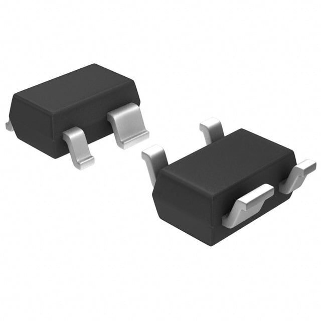
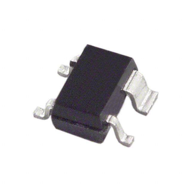
| 产品图片 |
|
| rohs | 符合RoHS无铅 / 符合限制有害物质指令(RoHS)规范要求 |
| 产品系列 | 电源管理 IC,监控电路,Maxim Integrated MAX6711TEXS+T- |
| NumberofInputsMonitored | 1 Input |
| 数据手册 | |
| 产品型号 | MAX6711TEXS+T |
| 产品培训模块 | http://www.digikey.cn/PTM/IndividualPTM.page?site=cn&lang=zhs&ptm=25703http://www.digikey.cn/PTM/IndividualPTM.page?site=cn&lang=zhs&ptm=25705 |
| 产品目录页面 | |
| 产品种类 | 监控电路 |
| 人工复位 | Manual Reset |
| 供应商器件封装 | SC-70-4 |
| 其它名称 | MAX6711TEXS+TCT |
| 功率失效检测 | No |
| 包装 | 剪切带 (CT) |
| 受监控电压数 | 1 |
| 商标 | Maxim Integrated |
| 复位 | 低有效 |
| 复位超时 | 最小为 140 ms |
| 安装类型 | 表面贴装 |
| 安装风格 | SMD/SMT |
| 封装 | Reel |
| 封装/外壳 | SC-82A,SOT-343 |
| 封装/箱体 | SC-70-4L |
| 工作温度 | -40°C ~ 125°C |
| 工作电源电流 | 12 uA |
| 工厂包装数量 | 2500 |
| 最大功率耗散 | 245 mW |
| 最大工作温度 | + 125 C |
| 最小工作温度 | - 40 C |
| 标准包装 | 1 |
| 欠电压阈值 | 3.04 V |
| 电压-阈值 | 3.08V |
| 电池备用开关 | No Backup |
| 电源电压-最大 | 5.5 V |
| 电源电压-最小 | 1.2 V |
| 监视器 | No Watchdog |
| 类型 | Voltage Supervisory |
| 系列 | MAX6711T |
| 芯片启用信号 | No Chip Enable |
| 被监测输入数 | 1 Input |
| 输出 | 推挽式,图腾柱 |
| 输出类型 | Active Low, Push-Pull |
| 过电压阈值 | 3.11 V |
| 重置延迟时间 | 640 ms |
| 阈值电压 | 2.5 V, 3 V, 3.3 V, 5 V |
| 零件号别名 | MAX6711T |


- 商务部:美国ITC正式对集成电路等产品启动337调查
- 曝三星4nm工艺存在良率问题 高通将骁龙8 Gen1或转产台积电
- 太阳诱电将投资9.5亿元在常州建新厂生产MLCC 预计2023年完工
- 英特尔发布欧洲新工厂建设计划 深化IDM 2.0 战略
- 台积电先进制程称霸业界 有大客户加持明年业绩稳了
- 达到5530亿美元!SIA预计今年全球半导体销售额将创下新高
- 英特尔拟将自动驾驶子公司Mobileye上市 估值或超500亿美元
- 三星加码芯片和SET,合并消费电子和移动部门,撤换高东真等 CEO
- 三星电子宣布重大人事变动 还合并消费电子和移动部门
- 海关总署:前11个月进口集成电路产品价值2.52万亿元 增长14.8%


PDF Datasheet 数据手册内容提取
MAX6711L/M/R/S/T/Z, 4-Pin SC70 Microprocessor MAX6712L/M/R/S/T/Z, Reset Circuits with Manual Reset Input MAX6713L/M/R/S/T/Z General Description Features The MAX6711/MAX6712/MAX6713 are microprocessor ● Precision Monitoring of 2.5V, 3.0V, 3.3V, and 5.0V (µP) supervisory circuits used to monitor the power Power-Supply Voltages supplies in µP and digital systems. They provide ● Fully Specified Over Temperature excellent circuit reliability and low cost by eliminating exter- ● Available in Three Output Configurations nal components and adjustments when used with Push-Pull RESET Output (MAX6711) +5.0V, +3.3V, +3.0V, or +2.5V-powered circuits. They Push-Pull RESET Output (MAX6712) also provide a debounced manual reset input. Open-Drain RESET Output (MAX6713) These circuits assert a reset signal whenever the VCC ● 140ms min Power-On-Reset Pulse Width supply voltage declines below a preset threshold or ● Manual Reset Input whenever manual reset is asserted. Reset remains asserted for at least 140ms after VCC has risen above ● 12µA Supply Current the reset threshold or when manual reset is deasserted. ● Guaranteed Reset Valid to VCC = +1V Reset thresholds suitable for operation with a variety of ● Power-Supply Transient Immunity supply voltages are available. ● No External Components The MAX6713 has an open-drain output stage, while ● 4-Pin SC70 Package the MAX6711/MAX6712 have push-pull outputs. The MAX6713’s open-drain RESET output requires a pull-up Ordering Information resistor that can be connected to a voltage higher than PART TEMP RANGE PIN-PACKAGE VCC. The MAX6711/MAX6713 have an active-low reset output, while the MAX6712 has an active-high reset out- MAX6711_EXS-T -40°C to +125°C 4 SC70 put. The reset comparator is designed to ignore fast MAX6711_EXS-T10 -40°C to +125°C 4 SC70 transients on VCC, and the outputs are guaranteed to MAX6712_EXS-T -40°C to +125°C 4 SC70 be in the correct logic state for VCC down to 1V. MAX6712_EXS-T10 -40°C to +125°C 4 SC70 Low supply current makes the MAX6711/MAX6712/ MAX6713 ideal for use in portable equipment. These MAX6713_EXS-T -40°C to +125°C 4 SC70 devices are available in a 4-pin SC70 package. MAX6713_EXS-T10 -40°C to +125°C 4 SC70 Note: These parts are offered in 2.5k or 10k reels and must Applications be ordered in 2.5k or 10k increments. Order MAX6711_EXS-T ● Computers ● Portable/Battery- for 2.5k reels and MAX6711_EXS-T10 for 10k reels. Insert the desired suffix letter from the Selector Guide into the blank to ● Controllers Powered Equipment complete the part number. ● Intelligent Instruments Devices are available in both leaded and lead-free packaging. ● Critical µP and µC Specify lead-free by replacing “-T” with “+T” when ordering. Power Monitoring Selector Guide appears at end of data sheet. Typical Operating Circuit Pin Configuration VCC TOP VIEW VCC VCC GND 1 4 VCC RPULL-UP* MMAAXX66771113 µP MAX6711 PUSHBUTTON RESET RINEPSUETT MMAAXX66771123 SWITCH MR GND GND RESET (RESET) 2 3 MR SC70-4 *MAX6713 ONLY ( ) ARE FOR MAX6712. 19-1623; Rev 2; 5/14
MAX6711L/M/R/S/T/Z, 4-Pin SC70 Microprocessor MAX6712L/M/R/S/T/Z, Reset Circuits with Manual Reset Input MAX6713L/M/R/S/T/Z Absolute Maximum Ratings Terminal Voltage (with respect to GND) Rate of Rise, VCC ..........................................................100V/µs VCC .......................................................................-0.3V to +6.0V Continuous Power Dissipation (TA = +70°C) RESET, RESET (push-pull) ......................-0.3V to (VCC + 0.3V) 4-Pin SC70 (derate 3.1mW/°C above +70°C) .............245mW RESET (open drain) .............................................-0.3V to +6.0V Operating Temperature Range .........................-40°C to +125°C MR ............................................................-0.3V to (VCC + 0.3V) Storage Temperature Range ............................-65°C to +150°C Input Current, VCC, MR ......................................................20mA Lead Temperature (soldering, 10s) .................................+300°C Output Current, RESET, RESET ........................................20mA Stresses beyond those listed under “Absolute Maximum Ratings” may cause permanent damage to the device. These are stress ratings only, and functional operation of the device at these or any other conditions beyond those indicated in the operational sections of the specifications is not implied. Exposure to absolute maximum rating conditions for extended periods may affect device reliability. Electrical Characteristics (VCC = full range, TA = -40°C to +125°C, unless otherwise noted. Typical values are at VCC = +5V for L/M versions, VCC = +3.3V for T/S versions, VCC = +3V for R version, VCC = +2.5V for Z version, and TA = +25°C.) (Note 1) PARAMETER SYMBOL CONDITIONS MIN TYP MAX UNITS TA = 0°C to +70°C 1.0 5.5 VCC Range V TA = -40°C to +105°C 1.2 5.5 TA = -40°C to VCC < 5.5V, MAX671_L/M 16 35 +85°C VCC < 3.6V, MAX671_R/S/T/Z 12 30 Supply Current ICC µA TA = +85°C to VCC < 5.5V, MAX671_L/M 75 +105°C VCC < 3.6V, MAX671_R/S/T/Z 75 TA = +25°C 4.56 4.63 4.70 MAX671_L TA = -40°C to +85°C 4.50 4.75 TA = +85°C to +105°C 4.40 4.86 TA = +25°C 4.31 4.38 4.45 MAX671_M TA = -40°C to +85°C 4.25 4.50 TA = +85°C to +105°C 4.16 4.56 TA = +25°C 3.04 3.08 3.11 MAX671_T TA = -40°C to +85°C 3.00 3.15 TA = +85°C to +105°C 2.92 3.23 Reset Threshold VTH V TA = +25°C 2.89 2.93 2.96 MAX671_S TA = -40°C to +85°C 2.85 3.00 TA = +85°C to +105°C 2.78 3.08 TA = +25°C 2.59 2.63 2.66 MAX671_R TA = -40°C to +85°C 2.55 2.70 TA = +85°C to +105°C 2.50 2.76 TA = +25°C 2.28 2.32 2.35 MAX671_Z TA = -40°C to +85°C 2.25 2.38 TA = +85°C to +105°C 2.21 2.45 Reset-Threshold Tempco 30 ppm/°C VCC to Reset Delay (Note 2) VCC = VTH to (VTH - 100 mV) 20 µs TA = -40°C to +85°C 140 240 460 Reset Active Timeout Period ms TA = +85°C to +125°C 100 840 www.maximintegrated.com Maxim Integrated │ 2
MAX6711L/M/R/S/T/Z, 4-Pin SC70 Microprocessor MAX6712L/M/R/S/T/Z, Reset Circuits with Manual Reset Input MAX6713L/M/R/S/T/Z Electrical Characteristics (continued) (VCC = full range, TA = -40°C to +125°C, unless otherwise noted. Typical values are at VCC = +5V for L/M versions, VCC = +3.3V for T/S versions, VCC = +3V for R version, VCC = +2.5V for Z version, and TA = +25°C.) (Note 1) PARAMETER SYMBOL CONDITIONS MIN TYP MAX UNITS VCC = VTH min, ISINK = 1.2mA, 0.3 MAX6711R/S/T/Z, MAX6713R/S/T/Z RESET Output-Voltage Low VOL VCC = VTH min, ISINK = 3.2mA, V (MAX6711/MAX6713) 0.4 MAX6711L/M, MAX6713L/M VCC > 1.0V, ISINK = 50µA 0.3 VCC > VTH max, ISOURCE = 500µA, 0.8 x VCC RESET Output-Voltage High MAX6711R/S/T/Z VOH V (MAX6711) VCC > VTH max, ISOURCE = 800µA, VCC x 1.5 MAX6711L/M VCC = VTH max, ISINK = 1.2mA, VOL 0.3 RESET Output-Voltage Low MAX6712R/S/T/Z V (MAX6712) VCC = VTH max, ISINK = 3.2mA, MAX6712L/M 0.4 RESET Output-Voltage High VOH 1.8V < VCC < VTH min, ISOURCE = 150µA 0.8 x VCC V (MAX6712) RESET Open-Drain Output- VCC > VTH, RESET deasserted 1 µA Leakage Current VIL 0.3 x VCC MR Input Threshold V VIH 0.7 x VCC MR Pull-Up Resistance 10 20 kW MR Minimum Pulse Width 1 µs MR Glitch Immunity 100 ns MR to Reset Delay 200 ns Note 1: Production testing done at TA = +25°C; limits over temperature guaranteed by design only. Note 2: RESET output for MAX6711/MAX6713; RESET output for MAX6712. www.maximintegrated.com Maxim Integrated │ 3
MAX6711L/M/R/S/T/Z, 4-Pin SC70 Microprocessor MAX6712L/M/R/S/T/Z, Reset Circuits with Manual Reset Input MAX6713L/M/R/S/T/Z Typical Operating Characteristics (VCC = full range, TA = -40°C to +125°C, unless otherwise noted. Typical values are at VCC = +5V for L/M versions, VCC = +3.3V for T/S versions, VCC = +3V for R version, VCC = +2.5V for Z version, and TA = +25°C.) SUPPLY CURRENT vs. TEMPERATURE MAX671_R/S/T/Z MAX671_L/M (NO LOAD) POWER-DOWN RESET DELAY vs. TEMPERATURE POWER-DOWN RESET DELAY vs. TEMPERATURE µSUPPLY CURRENT (A) 11505 MAXM6A71XM 6_A7R1X/_S6L/7T/1M, V_, LVC/CCM C=/R =M3/ S.5A3/VXVT6/Z7,1 V _CZC, =V C1CV = 2.5V MAX6711/12/13 toc01 µPOWER-DOWN RESET DELAY (s) 84260000 VVVOOODDD = == 1 21000mm0VmVV MAX6711/12/13-TOC2 µPOWER-DOWN RESET DELAY (s)111258639000000 VODVV O=OD 1D =0 = 02 m100mVmVV MAX6711/12/13-TOC3 0 0 VOD = 200mV 0 VOD = 200mV -40 -20 0 20 40 60 80 100 120 -40 -20 0 20 40 60 80 100 120 -40 -20 0 20 40 60 80 100 120 TEMPERATURE (°C) TEMPERATURE (°C) TEMPERATURE (°C) POWER-UP RESET TIMEOUT vs. RESET THRESHOLD vs. TEMPERATURE TEMPERATURE MEOUT (ms) 320705 MAX6711/12/13-TOC4 OLD (V) 11..000010 VTH = 4.63V MAX6711/12/13-TOC5 R-UP RESET TI 250 MAX671_ R/S/T/Z ESET THRESH 0.999 E R W 225 O P MAX671_ L/M 200 0.998 -40 -20 0 20 40 60 80 100 120 -40 -20 0 20 40 60 80 100 120 TEMPERATURE (°C) TEMPERATURE (°C) www.maximintegrated.com Maxim Integrated │ 4
MAX6711L/M/R/S/T/Z, 4-Pin SC70 Microprocessor MAX6712L/M/R/S/T/Z, Reset Circuits with Manual Reset Input MAX6713L/M/R/S/T/Z Pin Description PIN NAME FUNCTION VCC 1 GND Ground MAX6711 RESET RESET output remains low while (MAX6711/ VCC is below the reset threshold, and RESET for at least 140ms after VCC rises MAX6713) above the reset threshold. MR R1 2 GND 100k RESET output remains high while RESET VCC is below the reset threshold, and (MAX6712) for at least 140ms after VCC rises Figure 2. RESET Valid to VCC = Ground Circuit above the reset threshold. Manual Reset Input. RESET (RESET) remains asserted as long as MR is least 140ms after VCC has risen above the reset thresh- low, and for at least 140ms after MR is old. The MAX6713 uses an open-drain output, and deasserted. This active-low input has the MAX6711/MAX6712 have a push-pull output stage. 3 MR an internal 20kW(typ) pull-up resistor. Connect a pull-up resistor on the MAX6713's RESET It can be driven from a TTL- or output to any supply between 0 and 6V. CMOS- logic line, or shorted to ground with a switch. Leave open or connect Manual Reset Input to VCC if unused. Many µP-based systems require manual reset capabili- Supply Voltage (+5.0V, +3.3V, +3.0V, ty, allowing the operator, a test technician, or external 4 VCC or +2.5V) logic circuitry to initiate a reset. Reset remains asserted while MR is low, and for at least 140ms after MR returns high. This input has an internal 20kW pullup resistor, so 400 it can be left open if it is not used. MR can be driven µs) TA = +25C with TTL- or CMOS-logic levels, or with open-drain/col- ON ( 320 lector outputs. To create a manual reset function, con- TI A R nect a normally open momentary switch from MR to U T D 240 ground; external debounce circuitry is not required. If N E SI MR is driven from long cables or if the device is used in N TRA 160 a noisy environment, connecting a 0.1µF capacitor from UM MAX671_L/M MR to ground provides additional noise immunity. M XI 80 A M MAX671_R/S/T/Z Applications Information 0 1 10 100 1000 RESET COMPARATOR OVERDRIVE, VTH - VCC (mV) Negative-Going VCC Transients Figure 1. Maximum Transient Duration Without Causing a In addition to issuing a reset to the µP during power-up, Reset Pulse vs. Reset Comparator Overdrive power-down, and brownout conditions, the MAX6711/ MAX6712/MAX6713 are relatively immune to short-dura- tion negative-going VCC transients (glitches). Figure 1 shows typical transient duration vs. reset com- Detailed Description parator overdrive, for which the MAX6711/MAX6712/ MAX6713 do not generate a reset pulse. The graph was Reset Output generated using a negative-going pulse applied to VCC, A microprocessor's (µP's) reset input starts the µP in a starting 0.5V above the actual reset threshold and end- known state. The MAX6711/MAX6712/MAX6713 assert ing below it by the magnitude indicated (reset compar- reset to prevent code-execution errors during power- ator overdrive). The graph indicates the maximum pulse up, power-down, or brownout conditions. They assert a width a negative-going VCC transient can have without reset signal whenever the VCC supply voltage declines causing a reset pulse. As the magnitude of the transient below a preset threshold, keeping it asserted for at increases (goes farther below the reset threshold), the www.maximintegrated.com Maxim Integrated │ 5
MAX6711L/M/R/S/T/Z, 4-Pin SC70 Microprocessor MAX6712L/M/R/S/T/Z, Reset Circuits with Manual Reset Input MAX6713L/M/R/S/T/Z +5.0V VCC +3.3V VCC VCC VCC VCC MAX6713 µP RPULLUP 5V SYSTEM MAX6713 MOTOROLA RESET 68HCXX RESET INPUT RESET RESET INPUT MR GND GND GND GND Figure 3. Interfacing to μPs with Bidirectional Reset I/O Figure 4. MAX6713 Open-Drain RESET Output Allows Use with Multiple Supplies maximum allowable pulse width decreases. Typically, MAX6713 Open-Drain RESET Output for the MAX671_L and MAX671_M, a VCC transient that Allows Use with Multiple Supplies goes 100mV below the reset threshold and lasts 20µs or Generally, the pull-up connected to the MAX6713 will less will not cause a reset pulse. A 0.1µF bypass capaci- connect to the supply voltage that is being monitored at tor mounted as close as possible to the VCC pin provides the IC's VCC pin. However, some systems may use the additional transient immunity. open-drain output to level-shift from the monitored sup- ply to reset circuitry powered by some other supply Ensuring a Valid Reset Output Down to VCC = 0 (Figure 4). Note that as the MAX6713's VCC decreases below 1V, so does the IC's ability to sink current at When VCC falls below 1V, the MAX6711 RESET output RESET. Also, with any pullup, RESET will be pulled high no longer sinks current—it becomes an open circuit. as VCC decays toward 0. The voltage where this occurs Therefore, high-impedance CMOS-logic inputs connect- depends on the pull-up resistor value and the voltage ed to RESET can drift to undetermined voltages. This to which it is connected. presents no problem in most applications since most µP and other circuitry is inoperative with VCC below 1V. Benefits of Highly Accurate However, in applications where RESET must be valid Reset Threshold down to 0, adding a pull-down resistor to RESET caus- Most µP supervisor ICs have reset threshold voltages es any stray leakage currents to flow to ground, holding between 5% and 10% below the value of nominal supply RESET low (Figure 2). R1's value is not critical; 100kW is voltages. This ensures a reset will not occur within 5% of large enough not to load RESET and small enough to pull the nominal supply, but will occur when the supply is 10% RESET to ground. below nominal. A 100kW pull-up resistor to VCC is also recommended When using ICs rated at only the nominal supply ±5%, for the MAX6712 if RESET is required to remain valid for a zone of uncertainty where the supply is between 5% VCC < 1V.66 and 10% low, and where the reset may or may not be asserted is left. Interfacing to µPs with Bidirectional Reset Pins The MAX671_L/T/Z use highly accurate circuitry to Since the RESET output on the MAX6713 is open- ensure that reset is asserted close to the 5% limit, drain, this device interfaces easily with µPs that have and long before the supply has declined to 10% below bidirectional reset pins, such as the Motorola 68HC11. nominal. Connecting the µP supervisor's RESET output directly to the µP's RESET pin with a single pull-up resistor allows Chip Information either device to assert reset (Figure 3). TRANSISTOR COUNT: 380 www.maximintegrated.com Maxim Integrated │ 6
MAX6711L/M/R/S/T/Z, 4-Pin SC70 Microprocessor MAX6712L/M/R/S/T/Z, Reset Circuits with Manual Reset Input MAX6713L/M/R/S/T/Z Selector Guide PART/SUFFIX RESET THRESHOLD (V) OUTPUT TYPE TOP MARK MAX6711L 4.63 Push-Pull RESET AAB MAX6711M 4.38 Push-Pull RESET AAC MAX6711T 3.08 Push-Pull RESET AAD MAX6711S 2.93 Push-Pull RESET AAE MAX6711R 2.63 Push-Pull RESET AAF MAX6711Z 2.32 Push-Pull RESET AAG MAX6712L 4.63 Push-Pull RESET AAH MAX6712M 4.38 Push-Pull RESET AAI MAX6712T 3.08 Push-Pull RESET AAJ MAX6712S 2.93 Push-Pull RESET AAK MAX6712R 2.63 Push-Pull RESET AAL MAX6712Z 2.32 Push-Pull RESET AAM MAX6713L 4.63 Open-Drain RESET AAN MAX6713M 4.38 Open-Drain RESET AAO MAX6713T 3.08 Open-Drain RESET AAP MAX6713S 2.93 Open-Drain RESET AAQ MAX6713R 2.63 Open-Drain RESET AAR MAX6713Z 2.32 Open-Drain RESET AAS Package Information For the latest package outline information and land patterns (footprints), go to www.maximintegrated.com/packages. Note that a “+”, “#”, or “-” in the package code indicates RoHS status only. Package drawings may show a different suffix character, but the drawing pertains to the package regardless of RoHS status. PACKAGE PACKAGE OUTLINE LAND TYPE CODE NO. PATTERN NO. 4 SC70 X4-1 21-0098 90-0187 www.maximintegrated.com Maxim Integrated │ 7
MAX6711L/M/R/S/T/Z, 4-Pin SC70 Microprocessor MAX6712L/M/R/S/T/Z, Reset Circuits with Manual Reset Input MAX6713L/M/R/S/T/Z Revision History REVISION REVISION PAGES DESCRIPTION NUMBER DATE CHANGED 2 5/14 No /V OPNs; removed automotive reference from Applications section 1 For pricing, delivery, and ordering information, please contact Maxim Direct at 1-888-629-4642, or visit Maxim Integrated’s website at www.maximintegrated.com. Maxim Integrated cannot assume responsibility for use of any circuitry other than circuitry entirely embodied in a Maxim Integrated product. No circuit patent licenses are implied. Maxim Integrated reserves the right to change the circuitry and specifications without notice at any time. The parametric values (min and max limits) shown in the Electrical Characteristics table are guaranteed. Other parametric values quoted in this data sheet are provided for guidance. Maxim Integrated and the Maxim Integrated logo are trademarks of Maxim Integrated Products, Inc. © 2014 Maxim Integrated Products, Inc. │ 8
Mouser Electronics Authorized Distributor Click to View Pricing, Inventory, Delivery & Lifecycle Information: M axim Integrated: MAX6711LEXS+T MAX6711REXS+T MAX6711SEXS+T MAX6711TEXS+T MAX6711ZEXS+T MAX6713LEXS+T MAX6713MEXS+T MAX6713REXS+T MAX6713SEXS+T MAX6713TEXS+T MAX6713ZEXS+T MAX6711LEXS+T10 MAX6711MEXS+T MAX6711MEXS+T10 MAX6711REXS+T10 MAX6711SEXS+T10 MAX6711TEXS+T10 MAX6711ZEXS+T10 MAX6712LEXS+T MAX6712LEXS+T10 MAX6712MEXS+T MAX6712MEXS+T10 MAX6712REXS+T MAX6712REXS+T10 MAX6712SEXS+T MAX6712SEXS+T10 MAX6712TEXS+T MAX6712TEXS+T10 MAX6712ZEXS+T MAX6712ZEXS+T10 MAX6713LEXS+T10 MAX6713MEXS+T10 MAX6713REXS+T10 MAX6713SEXS+T10 MAX6713TEXS+T10 MAX6713ZEXS+T10 MAX6711LEXS+