ICGOO在线商城 > 集成电路(IC) > PMIC - 监控器 > TPS3837K33QDBVREP
 Datasheet下载
- 型号: TPS3837K33QDBVREP
- 制造商: Texas Instruments
- 库位|库存: xxxx|xxxx
- 要求:
| 数量阶梯 | 香港交货 | 国内含税 |
| +xxxx | $xxxx | ¥xxxx |
查看当月历史价格
查看今年历史价格
TPS3837K33QDBVREP产品简介:
ICGOO电子元器件商城为您提供TPS3837K33QDBVREP由Texas Instruments设计生产,在icgoo商城现货销售,并且可以通过原厂、代理商等渠道进行代购。 TPS3837K33QDBVREP价格参考。Texas InstrumentsTPS3837K33QDBVREP封装/规格:PMIC - 监控器, 推挽式,图腾柱 监控器 1 通道 SOT-23-5。您可以下载TPS3837K33QDBVREP参考资料、Datasheet数据手册功能说明书,资料中有TPS3837K33QDBVREP 详细功能的应用电路图电压和使用方法及教程。
TPS3837K33QDBVREP是德州仪器(Texas Instruments)生产的PMIC(电源管理集成电路)监控器,主要用于电压监控和复位功能。以下是该型号的应用场景:

1. 工业控制系统:在工业自动化设备中,TPS3837K33QDBVREP可以用于监控关键电源轨的电压水平,确保系统在启动、运行和关闭过程中保持稳定。它能够检测到电压异常并触发复位信号,防止系统因电源问题而出现故障。

2. 通信设备:在网络路由器、交换机和其他通信基础设施中,该器件可以监控电源电压,确保设备在各种工作条件下都能正常运行。它可以在电压跌落或过压时提供保护,避免硬件损坏。

3. 消费电子:在智能电视、平板电脑和其他消费电子产品中,TPS3837K33QDBVREP可以用于监控主电源和辅助电源的电压状态,确保设备在低功耗模式下也能可靠工作。它还可以帮助设备在电源恢复后快速恢复正常操作。

4. 汽车电子:在车载信息娱乐系统、ADAS(高级驾驶辅助系统)等汽车电子应用中,该器件可以监控电池电压和稳压器输出电压,确保系统的稳定性和安全性。它能够在电压异常时触发复位,避免系统崩溃或数据丢失。

5. 医疗设备:在便携式医疗设备如血糖仪、心电图机等中,TPS3837K33QDBVREP可以用于监控电源电压,确保设备在电池供电或外部电源供电的情况下都能正常工作。它还能在电压异常时提供保护,确保患者安全。

6. 服务器和数据中心:在服务器和数据中心设备中,该器件可以用于监控多个电源轨的电压,确保系统在高负载或突发情况下仍能稳定运行。它可以在电压波动时提供复位信号,防止系统崩溃或数据丢失。

总之,TPS3837K33QDBVREP适用于需要高可靠性电源监控和复位功能的各种应用场景,广泛应用于工业、通信、消费、汽车、医疗和数据中心等领域。
| 参数 | 数值 |
| 产品目录 | 集成电路 (IC) |
| 描述 | IC LP SUPERVISRY CIRCUIT SOT23-5 |
| 产品分类 | |
| 品牌 | Texas Instruments |
| 数据手册 | |
| 产品图片 |
|
| 产品型号 | TPS3837K33QDBVREP |
| rohs | 无铅 / 符合限制有害物质指令(RoHS)规范要求 |
| 产品系列 | - |
| 产品目录页面 | |
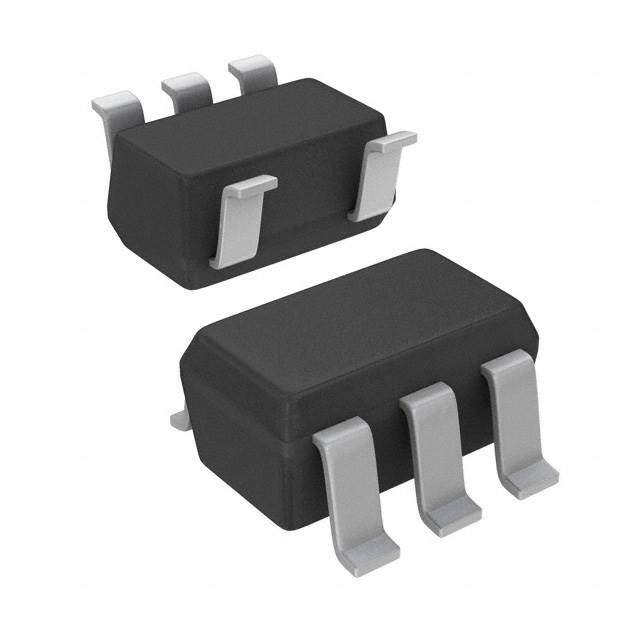
| 供应商器件封装 | SOT-23-5 |
| 其它名称 | 296-20786-6 |
| 包装 | Digi-Reel® |
| 受监控电压数 | 1 |
| 复位 | 高有效 |
| 复位超时 | 最小为 100 ms |
| 安装类型 | 表面贴装 |
| 封装/外壳 | SC-74A,SOT-753 |
| 工作温度 | -40°C ~ 125°C |
| 标准包装 | 1 |
| 电压-阈值 | 2.93V |
| 类型 | 简单复位/加电复位 |
| 输出 | 推挽式,图腾柱 |


- 商务部:美国ITC正式对集成电路等产品启动337调查
- 曝三星4nm工艺存在良率问题 高通将骁龙8 Gen1或转产台积电
- 太阳诱电将投资9.5亿元在常州建新厂生产MLCC 预计2023年完工
- 英特尔发布欧洲新工厂建设计划 深化IDM 2.0 战略
- 台积电先进制程称霸业界 有大客户加持明年业绩稳了
- 达到5530亿美元!SIA预计今年全球半导体销售额将创下新高
- 英特尔拟将自动驾驶子公司Mobileye上市 估值或超500亿美元
- 三星加码芯片和SET,合并消费电子和移动部门,撤换高东真等 CEO
- 三星电子宣布重大人事变动 还合并消费电子和移动部门
- 海关总署:前11个月进口集成电路产品价值2.52万亿元 增长14.8%


PDF Datasheet 数据手册内容提取
TPS3836E18-EP / J25-EP / H30-EP / L30-EP / K33-EP TPS3837E18-EP / J25-EP / L30-EP / K33-EP TPS3838E18-EP / J25-EP / L30-EP / K33-EP www.ti.com.................................................................................................................................................... SGLS322D–MAY2006–REVISEDNOVEMBER2008 NANOPOWER SUPERVISORY CIRCUITS FEATURES 1 TPS3836, TPS3838 • ESDProtectionExceeds2000VPer DBV PACKAGE MIL-STD-883,Method3015;Exceeds200V (TOP VIEW) UsingMachineModel(C=200pF,R=0) • SupplyCurrentof220nA(Typ) CT 1 5 VDD • PrecisionSupplyVoltageSupervisionRange: GND 2 1.8V,2.5V,3V,3.3V • Power-OnResetGeneratorWithSelectable MR 3 4 RESET DelayTimeof10msor200ms • Push/PullRESETOutput(TPS3836), RESET TPS3837 Output(TPS3837),or DBV PACKAGE Open-DrainRESETOutput(TPS3838) (TOP VIEW) • ManualReset CT 1 5 VDD • 5-PinSOT-23Package GND 2 SUPPORTS DEFENSE, AEROSPACE, AND MEDICAL APPLICATIONS MR 3 4 RESET • ControlledBaseline • OneAssembly/TestSite • OneFabricationSite • AvailableinMilitary(–55°C/125°C) TemperatureRange(1) • ExtendedProductLifeCycle • ExtendedProduct-ChangeNotification • ProductTraceability APPLICATIONS • ApplicationsUsingAutomotiveLow-Power DSPs,Microcontrollers,orMicroprocessors • Battery-PoweredEquipment • IntelligentInstruments • WirelessCommunicationSystems • AutomotiveSystems (1) Customtemperaturerangesavailable DESCRIPTION The TPS3836, TPS3837, TPS3838 families of supervisory circuits provide circuit initialization and timing supervision,primarilyfordigitalsignalprocessing(DSP)andprocessor-basedsystems. During power on, RESET is asserted when the supply voltage V becomes higher than 1.1 V. Thereafter, the DD supervisory circuit monitors V and keeps RESET output active as long as V remains below the threshold DD DD voltage (V ). An internal timer delays the return of the output to the inactive state (high) to ensure proper system IT reset.ThedelaytimestartsafterV hasrisenaboveV . DD IT When CT is connected to GND, a fixed delay time of typical 10 ms is asserted. When connected to V , the DD delaytimeistypically200ms. 1 Pleasebeawarethatanimportantnoticeconcerningavailability,standardwarranty,anduseincriticalapplicationsofTexas Instrumentssemiconductorproductsanddisclaimerstheretoappearsattheendofthisdatasheet. PRODUCTIONDATAinformationiscurrentasofpublicationdate. Copyright©2006–2008,TexasInstrumentsIncorporated Products conform to specifications per the terms of the Texas Instruments standard warranty. Production processing does not necessarilyincludetestingofallparameters.
TPS3836E18-EP / J25-EP / H30-EP / L30-EP / K33-EP TPS3837E18-EP / J25-EP / L30-EP / K33-EP TPS3838E18-EP / J25-EP / L30-EP / K33-EP SGLS322D–MAY2006–REVISEDNOVEMBER2008.................................................................................................................................................... www.ti.com WhenthesupplyvoltagedropsbelowV ,theoutputbecomesactive(low)again. IT Allthedevicesofthisfamilyhaveafixed-senseV setbyaninternalvoltagedivider. IT The TPS3836 has an active-low push-pull RESET output. The TPS3837 has active-high push-pull RESET, and theTPS3838integratesanactive-lowopen-drainRESEToutput. TPS3836K33 MSP430 VDD VCC CT Xin Lithium RESET RST Battery MR Xout Quartz 3.6 V T GND VSS 32 kHz Figure1.TypicalOperatingCircuit Theproductspectrumisdesignedforsupplyvoltagesof1.8V,2.5V,3V,and3.3V. The circuits are available in a 5-pin SOT-23 package. The TPS3836, TPS3837, and TPS3838 families are characterized for operation over a temperaturerangeof–55°Cto125°C. 2 SubmitDocumentationFeedback Copyright©2006–2008,TexasInstrumentsIncorporated ProductFolderLink(s):TPS3836E18-EP/J25-EP/H30-EP/L30-EP/K33-EPTPS3837E18-EP/J25-EP/L30-EP/ K33-EPTPS3838E18-EP/J25-EP/L30-EP/K33-EP
TPS3836E18-EP / J25-EP / H30-EP / L30-EP / K33-EP TPS3837E18-EP / J25-EP / L30-EP / K33-EP TPS3838E18-EP / J25-EP / L30-EP / K33-EP www.ti.com.................................................................................................................................................... SGLS322D–MAY2006–REVISEDNOVEMBER2008 ORDERINGINFORMATION ORDERABLEPART TA NUMBER(1) THRESHOLDVOLTAGE SYMBOL TPS3836J25MDBVTEP 2.25V PKRM –55°Cto125°C TPS3836L30MDBVREP 2.64V BTX TPS3837K33MDBVREP 2.93V PKZM (1) DBVRindicatesreelof3000parts,DBVTindicatestapeof250parts. ORDERING INFORMATION TPS383 6 E 18 M DBV R/T EP EPDesignator Reel/Tape Package M-Temperature Designator Nominal SupplyVoltage Typical ResetThresholdVoltage Functionality Family FUNCTIONTABLE MR V >V RESET (1) RESET(2) DD IT L 0 L H L 1 L H H 0 L H H 1 H L (1) TPS3836andTPS3838 (2) TPS3837 Copyright©2006–2008,TexasInstrumentsIncorporated SubmitDocumentationFeedback 3 ProductFolderLink(s):TPS3836E18-EP/J25-EP/H30-EP/L30-EP/K33-EPTPS3837E18-EP/J25-EP/L30-EP/ K33-EPTPS3838E18-EP/J25-EP/L30-EP/K33-EP
TPS3836E18-EP / J25-EP / H30-EP / L30-EP / K33-EP TPS3837E18-EP / J25-EP / L30-EP / K33-EP TPS3838E18-EP / J25-EP / L30-EP / K33-EP SGLS322D–MAY2006–REVISEDNOVEMBER2008.................................................................................................................................................... www.ti.com FUNCTIONALBLOCKDIAGRAM VDD R3 CT MR R1 C1 Reset Logic RESET (TPS3837-Push-Pull) + and Timer S1 RESET (TPS3836-Push-Pull − TPS3838-Open-Drain) R2 C2 S2 S3 Band-Gap Reference C3 Refresh Timer GND 4 SubmitDocumentationFeedback Copyright©2006–2008,TexasInstrumentsIncorporated ProductFolderLink(s):TPS3836E18-EP/J25-EP/H30-EP/L30-EP/K33-EPTPS3837E18-EP/J25-EP/L30-EP/ K33-EPTPS3838E18-EP/J25-EP/L30-EP/K33-EP
TPS3836E18-EP / J25-EP / H30-EP / L30-EP / K33-EP TPS3837E18-EP / J25-EP / L30-EP / K33-EP TPS3838E18-EP / J25-EP / L30-EP / K33-EP www.ti.com.................................................................................................................................................... SGLS322D–MAY2006–REVISEDNOVEMBER2008 TIMING DIAGRAM A B C D E F G VDD VIT < 1.1 V t MR t RESET t Undefined td td td Undefined Output Output Absolute Maximum Ratings overoperatingfree-airtemperaturerange(unlessotherwisenoted) (1) V Supplyvoltage(2) 7V DD Allotherpins(2) –0.3Vto7V I Maximumlowoutputcurrent 5mA OL I Maximumhighoutputcurrent –5mA OH I Inputclampcurrent(V <0orV >V ) ±10mA IK I I DD I Outputclampcurrent(V <0orV >V ) ±10mA OK O O DD T Operatingfree-airtemperaturerange –55°Cto125°C A T Storagetemperaturerange –65°Cto150°C stg T Maximumjunctiontemperature 150°C J Solderingtemperature 260°C (1) Stressesbeyondthoselistedunderabsolutemaximumratingsmaycausepermanentdamagetothedevice.Thesearestressratings only,andfunctionaloperationofthedeviceattheseoranyotherconditionsbeyondthoseindicatedunderrecommendedoperating conditionsisnotimplied.Exposuretoabsolute-maximum-ratedconditionsforextendedperiodsmayaffectdevicereliability. (2) AllvoltagevaluesarewithrespecttoGND.Forreliableoperation,thedevicemustnotbecontinuouslyoperatedat7Vformorethan t=1000h. Copyright©2006–2008,TexasInstrumentsIncorporated SubmitDocumentationFeedback 5 ProductFolderLink(s):TPS3836E18-EP/J25-EP/H30-EP/L30-EP/K33-EPTPS3837E18-EP/J25-EP/L30-EP/ K33-EPTPS3838E18-EP/J25-EP/L30-EP/K33-EP
TPS3836E18-EP / J25-EP / H30-EP / L30-EP / K33-EP TPS3837E18-EP / J25-EP / L30-EP / K33-EP TPS3838E18-EP / J25-EP / L30-EP / K33-EP SGLS322D–MAY2006–REVISEDNOVEMBER2008.................................................................................................................................................... www.ti.com Thermal Resistance Table RESISTANCE HIGH LOW q (°C/W) 130.9 148.1 JC q (°C/W) 205.6 347 JA Recommended Operating Conditions MIN MAX UNIT V Supplyvoltage 1.6 6 V DD V Inputvoltage 0 V +0.3 V I DD V High-levelinputvoltage 0.7×V V IH DD V Low-levelinputvoltage 0.3×V V IL DD Δt/Δv InputtransitionriseandfallrateatMR 100 ns/V T Operatingfree-airtemperature –55 125 °C A Electrical Characteristics overrecommendedoperatingconditions(unlessotherwisenoted) PARAMETER TESTCONDITIONS MIN TYP MAX UNIT RESET VDD=3.3V,IOH=–2mA High-leveloutput (TPS3836) VDD=6V,IOH=–3mA V 0.8×V V OH voltage RESET VDD=2V,IOH=–1mA DD (TPS3837) V =3.3V,I =–2mA DD OH RESET VDD=2V,IOL=1mA Low-leveloutput (TPS3836/8) VDD=3.3V,IOL=2mA V 0.4 V OL voltage RESET VDD=3.3V,IOL=2mA (TPS3837) V =6V,I =3mA DD OL TPS3836/8 V ≥1.1V,I =50m A 0.2 DD OL Power-upreset voltage(1) TPS3837 V ≥1.1V,I =–50m A TA=25°C 0.8×VDD V DD OH T =Fullrange 0.6×V A DD TPS383xE18 1.64 1.71 1.73 TPS383xJ25 2.16 2.25 2.31 Negative-going TPS383xH30 2.7 2.79 2.85 V inputthreshold V IT voltage(2) TPS383xL30 2.54 2.64 2.71 T =25°C 2.82 2.93 3.1 A TPS383xK33 T =Fullrange 2.72 2.93 3.2 A 1.7V<V <2.5V 30 IT V HysteresisatV input 2.5V<V <3.5V 40 mV hys DD IT 3.5V<V <5V 50 IT T =25°C –30 –60 –90 High-levelinput MR (3) MR=0.7×VDD,VDD=6V A m A I T =Fullrange –20 –60 –120 IH current A CT CT=V =6V –25 25 nA DD T =25°C –130 –200 –340 Low-levelinput MR (3) MR=0V,VDD=6V A m A I T =Fullrange –90 –200 –350 IL current A CT CT=0V,V =6V –25 25 nA DD High-leveloutput I TPS3838 V =V +0.2V,V =V 25 nA OH current DD IT OH DD (1) ThelowestvoltageatwhichRESEToutputbecomesactive,t,V ≥15m s/V r DD (2) Toensurebeststabilityofthethresholdvoltage,abypasscapacitor(ceramic,0.1m F)shouldbeplacednearthesupplyterminal. (3) Ifmanualresetisunused,MRshouldbeconnectedtoV tominimizecurrentconsumption. DD 6 SubmitDocumentationFeedback Copyright©2006–2008,TexasInstrumentsIncorporated ProductFolderLink(s):TPS3836E18-EP/J25-EP/H30-EP/L30-EP/K33-EPTPS3837E18-EP/J25-EP/L30-EP/ K33-EPTPS3838E18-EP/J25-EP/L30-EP/K33-EP
TPS3836E18-EP / J25-EP / H30-EP / L30-EP / K33-EP TPS3837E18-EP / J25-EP / L30-EP / K33-EP TPS3838E18-EP / J25-EP / L30-EP / K33-EP www.ti.com.................................................................................................................................................... SGLS322D–MAY2006–REVISEDNOVEMBER2008 Electrical Characteristics (continued) overrecommendedoperatingconditions(unlessotherwisenoted) PARAMETER TESTCONDITIONS MIN TYP MAX UNIT T =25°C 220 500 A V >V ,V <3V DD IT DD T =Fullrange 600 A nA T =25°C 250 550 A I Supplycurrent V >V ,V >3V DD DD IT DD T =Fullrange 650 A T =25°C 10 25 V <V A m A DD IT T =Fullrange 30 A InternalpullupresistoratMR 33 kΩ C InputcapacitanceatMR,CT V =0VtoV 5 pF I I DD Timing Requirements R =1MΩ,C =50pF,T =25°C L L A PARAMETER TESTCONDITIONS TYP UNIT AtV V =V +0.2V,V =V –0.2V 6 m s DD IH IT IL IT t Pulsewidth w AtMR V ≥V +0.2V,V =0.3×V ,V =0.7×V 1 m s DD IT IL DD IH DD Switching Characteristics R =1MΩ,C =50pF,T =25°C L L A PARAMETER TESTCONDITIONS MIN TYP MAX UNIT V ≥V +0.2V,MR=0.7×V , CT=GND 5 10 15 t Delaytime DD IT DD ms d Seetimingdiagram CT=V 200 DD Propagation(delay) V toRESETdelay V =V –0.2V,V =V +0.2V 10 DD IL IT IH IT t time,high-tolow-level (TPS3836, m s PHL output TPS3838) VIL=1.6V 50 Propagation(delay) V =V –0.2V,V =V +0.2V 10 t time,low-tohigh-level VDDtoRESETdelay IL IT IH IT m s PLH output (TPS3837) VIL=1.6V 50 Propagation(delay) MRtoRESETdelay t time,high-tolow-level (TPS3836, V ≥V +0.2V,V =0.3×V ,V =0.7×V 0.3 m s PHL DD IT IL DD IH DD output TPS3838) Propagation(delay) t time,low-tohigh-level MRtoRESETdelay V ≥V +0.2V,V =0.3×V ,V =0.7×V 0.3 m s PLH (TPS3837) DD IT IL DD IH DD output Copyright©2006–2008,TexasInstrumentsIncorporated SubmitDocumentationFeedback 7 ProductFolderLink(s):TPS3836E18-EP/J25-EP/H30-EP/L30-EP/K33-EPTPS3837E18-EP/J25-EP/L30-EP/ K33-EPTPS3838E18-EP/J25-EP/L30-EP/K33-EP
TPS3836E18-EP / J25-EP / H30-EP / L30-EP / K33-EP TPS3837E18-EP / J25-EP / L30-EP / K33-EP TPS3838E18-EP / J25-EP / L30-EP / K33-EP SGLS322D–MAY2006–REVISEDNOVEMBER2008.................................................................................................................................................... www.ti.com TYPICAL CHARACTERISTICS TableofGraphs FIGURE I Supplycurrent vsSupplyvoltage 2 DD I Manualresetcurrent vsManualresetvoltage 3 MR V Low-leveloutputvoltage vsLow-leveloutputcurrent 4 OL V High-leveloutputvoltage vsHigh-leveloutputcurrent 5 OH Normalizedresetthresholdvoltage vsFree-airtemperature 6 MinimumpulsedurationatV vsV thresholdoverdrive 7 DD DD SUPPLYCURRENT MANUALRESETCURRENT vs vs SUPPLYVOLTAGE MANUALRESETVOLTAGE 10 100 MR = Open VDD = 6 V CT = GND TA = 85°C CT = GND 0 8 A A m− TA = −40°C mrent − 6 TA = 25°C Current −100 TA = 0°C Cur TA = 0°C set −200 y e ppl 4 al R TA = 25°C u u − SDD TA = −40°C − Man −300 TA = 85°C I R 2 M I −400 0 −500 0 2 4 6 −2 0 2 4 6 VDD − Supply Voltage − V VMR − Manual Reset Voltage − V Figure2. Figure3. 8 SubmitDocumentationFeedback Copyright©2006–2008,TexasInstrumentsIncorporated ProductFolderLink(s):TPS3836E18-EP/J25-EP/H30-EP/L30-EP/K33-EPTPS3837E18-EP/J25-EP/L30-EP/ K33-EPTPS3838E18-EP/J25-EP/L30-EP/K33-EP
TPS3836E18-EP / J25-EP / H30-EP / L30-EP / K33-EP TPS3837E18-EP / J25-EP / L30-EP / K33-EP TPS3838E18-EP / J25-EP / L30-EP / K33-EP www.ti.com.................................................................................................................................................... SGLS322D–MAY2006–REVISEDNOVEMBER2008 LOW-LEVELOUTPUTVOLTAGE HIGH-LEVELOUTPUTVOLTAGE vs vs LOW-LEVELOUTPUTCURRENT HIGH-LEVELOUTPUTCURRENT 2.0 2.0 VDD = 2 V VDD = 2 V MR = Open MR = Open CT = GND V V − CT = GND − Output Voltage 11..05 TA = 25°C Output Voltage 11..05 TTAA = = 8 255°°CC − Low-Level 0.5 TA = 85°C TA = 0°C − High-Level 0.5 TA = 0°C V OL TA = −40°C V OH TA = −40°C 0.0 0.0 0 1 2 3 4 5 6 7 0 1 2 3 4 5 IOL − Low-Level Output Current − mA IOH − High-Level Output Current − mA Figure4. Figure5. NORMALIZEDRESETTHRESHOLDVOLTAGE MINIMUMPULSEDURATIONATV DD vs vs FREE-AIRTEMPERATURE V THRESHOLDOVERDRIVE DD 1.001 22 MR = Open 20 V CT = GND e − 1 s 18 TA = 25°C oltag m − DD 16 V V old 0.999 n at 14 h o et Thres 0.998 e Durati 1102 s s ed Re 0.997 CT = GND m Pul 8 aliz MR = Open mu 6 m ni 4 or 0.996 Mi N 2 0.995 0 −40 −15 10 35 60 85 0 0.2 0.4 0.6 0.8 1 1.2 1.4 1.6 1.8 2 TA − Free-Air Temperature − °C VDD − Threshold Overdrive − V Figure6. Figure7. Copyright©2006–2008,TexasInstrumentsIncorporated SubmitDocumentationFeedback 9 ProductFolderLink(s):TPS3836E18-EP/J25-EP/H30-EP/L30-EP/K33-EPTPS3837E18-EP/J25-EP/L30-EP/ K33-EPTPS3838E18-EP/J25-EP/L30-EP/K33-EP
PACKAGE OPTION ADDENDUM www.ti.com 22-Dec-2016 PACKAGING INFORMATION Orderable Device Status Package Type Package Pins Package Eco Plan Lead/Ball Finish MSL Peak Temp Op Temp (°C) Device Marking Samples (1) Drawing Qty (2) (6) (3) (4/5) TPS3836J25MDBVTEP ACTIVE SOT-23 DBV 5 250 Green (RoHS CU NIPDAU Level-1-260C-UNLIM -55 to 125 PKRM & no Sb/Br) TPS3836L30MDBVREP ACTIVE SOT-23 DBV 5 3000 Green (RoHS CU NIPDAU Level-1-260C-UNLIM -55 to 125 BTX & no Sb/Br) TPS3837K33MDBVREP ACTIVE SOT-23 DBV 5 3000 Green (RoHS CU NIPDAU Level-1-260C-UNLIM -55 to 125 PKZM & no Sb/Br) TPS3837K33QDBVREP ACTIVE SOT-23 DBV 5 3000 Green (RoHS CU NIPDAU Level-1-260C-UNLIM -40 to 125 PLSQ & no Sb/Br) V62/06637-09XE ACTIVE SOT-23 DBV 5 3000 Green (RoHS CU NIPDAU Level-1-260C-UNLIM -40 to 125 PLSQ & no Sb/Br) V62/06637-15XE ACTIVE SOT-23 DBV 5 250 Green (RoHS CU NIPDAU Level-1-260C-UNLIM -55 to 125 PKRM & no Sb/Br) V62/06637-17XE ACTIVE SOT-23 DBV 5 3000 Green (RoHS CU NIPDAU Level-1-260C-UNLIM -55 to 125 BTX & no Sb/Br) V62/06637-22XE ACTIVE SOT-23 DBV 5 3000 Green (RoHS CU NIPDAU Level-1-260C-UNLIM -55 to 125 PKZM & no Sb/Br) (1) The marketing status values are defined as follows: ACTIVE: Product device recommended for new designs. LIFEBUY: TI has announced that the device will be discontinued, and a lifetime-buy period is in effect. NRND: Not recommended for new designs. Device is in production to support existing customers, but TI does not recommend using this part in a new design. PREVIEW: Device has been announced but is not in production. Samples may or may not be available. OBSOLETE: TI has discontinued the production of the device. (2) Eco Plan - The planned eco-friendly classification: Pb-Free (RoHS), Pb-Free (RoHS Exempt), or Green (RoHS & no Sb/Br) - please check http://www.ti.com/productcontent for the latest availability information and additional product content details. TBD: The Pb-Free/Green conversion plan has not been defined. Pb-Free (RoHS): TI's terms "Lead-Free" or "Pb-Free" mean semiconductor products that are compatible with the current RoHS requirements for all 6 substances, including the requirement that lead not exceed 0.1% by weight in homogeneous materials. Where designed to be soldered at high temperatures, TI Pb-Free products are suitable for use in specified lead-free processes. Pb-Free (RoHS Exempt): This component has a RoHS exemption for either 1) lead-based flip-chip solder bumps used between the die and package, or 2) lead-based die adhesive used between the die and leadframe. The component is otherwise considered Pb-Free (RoHS compatible) as defined above. Green (RoHS & no Sb/Br): TI defines "Green" to mean Pb-Free (RoHS compatible), and free of Bromine (Br) and Antimony (Sb) based flame retardants (Br or Sb do not exceed 0.1% by weight in homogeneous material) (3) MSL, Peak Temp. - The Moisture Sensitivity Level rating according to the JEDEC industry standard classifications, and peak solder temperature. Addendum-Page 1
PACKAGE OPTION ADDENDUM www.ti.com 22-Dec-2016 (4) There may be additional marking, which relates to the logo, the lot trace code information, or the environmental category on the device. (5) Multiple Device Markings will be inside parentheses. Only one Device Marking contained in parentheses and separated by a "~" will appear on a device. If a line is indented then it is a continuation of the previous line and the two combined represent the entire Device Marking for that device. (6) Lead/Ball Finish - Orderable Devices may have multiple material finish options. Finish options are separated by a vertical ruled line. Lead/Ball Finish values may wrap to two lines if the finish value exceeds the maximum column width. Important Information and Disclaimer:The information provided on this page represents TI's knowledge and belief as of the date that it is provided. TI bases its knowledge and belief on information provided by third parties, and makes no representation or warranty as to the accuracy of such information. Efforts are underway to better integrate information from third parties. TI has taken and continues to take reasonable steps to provide representative and accurate information but may not have conducted destructive testing or chemical analysis on incoming materials and chemicals. TI and TI suppliers consider certain information to be proprietary, and thus CAS numbers and other limited information may not be available for release. In no event shall TI's liability arising out of such information exceed the total purchase price of the TI part(s) at issue in this document sold by TI to Customer on an annual basis. OTHER QUALIFIED VERSIONS OF TPS3836-EP, TPS3836J25-EP, TPS3837K33-EP : •Catalog: TPS3836, TPS3836J25, TPS3837K33 •Automotive: TPS3836-Q1, TPS3836J25-Q1, TPS3837K33-Q1 NOTE: Qualified Version Definitions: •Catalog - TI's standard catalog product •Automotive - Q100 devices qualified for high-reliability automotive applications targeting zero defects Addendum-Page 2
PACKAGE MATERIALS INFORMATION www.ti.com 22-Dec-2016 TAPE AND REEL INFORMATION *Alldimensionsarenominal Device Package Package Pins SPQ Reel Reel A0 B0 K0 P1 W Pin1 Type Drawing Diameter Width (mm) (mm) (mm) (mm) (mm) Quadrant (mm) W1(mm) TPS3836J25MDBVTEP SOT-23 DBV 5 250 180.0 9.0 3.15 3.2 1.4 4.0 8.0 Q3 TPS3836L30MDBVREP SOT-23 DBV 5 3000 180.0 9.0 3.15 3.2 1.4 4.0 8.0 Q3 TPS3837K33MDBVREP SOT-23 DBV 5 3000 180.0 9.0 3.15 3.2 1.4 4.0 8.0 Q3 TPS3837K33QDBVREP SOT-23 DBV 5 3000 180.0 9.0 3.15 3.2 1.4 4.0 8.0 Q3 PackMaterials-Page1
PACKAGE MATERIALS INFORMATION www.ti.com 22-Dec-2016 *Alldimensionsarenominal Device PackageType PackageDrawing Pins SPQ Length(mm) Width(mm) Height(mm) TPS3836J25MDBVTEP SOT-23 DBV 5 250 182.0 182.0 20.0 TPS3836L30MDBVREP SOT-23 DBV 5 3000 182.0 182.0 20.0 TPS3837K33MDBVREP SOT-23 DBV 5 3000 182.0 182.0 20.0 TPS3837K33QDBVREP SOT-23 DBV 5 3000 182.0 182.0 20.0 PackMaterials-Page2
PACKAGE OUTLINE DBV0005A SOT-23 - 1.45 mm max height SCALE 4.000 SMALL OUTLINE TRANSISTOR C 3.0 2.6 0.1 C 1.75 1.45 B A 1.45 MAX PIN 1 INDEX AREA 1 5 2X 0.95 3.05 2.75 1.9 1.9 2 4 3 0.5 5X 0.3 0.15 0.2 C A B (1.1) TYP 0.00 0.25 GAGE PLANE 0.22 TYP 0.08 8 TYP 0.6 0 0.3 TYP SEATING PLANE 4214839/D 11/2018 NOTES: 1. All linear dimensions are in millimeters. Any dimensions in parenthesis are for reference only. Dimensioning and tolerancing per ASME Y14.5M. 2. This drawing is subject to change without notice. 3. Refernce JEDEC MO-178. 4. Body dimensions do not include mold flash, protrusions, or gate burrs. Mold flash, protrusions, or gate burrs shall not exceed 0.15 mm per side. www.ti.com
EXAMPLE BOARD LAYOUT DBV0005A SOT-23 - 1.45 mm max height SMALL OUTLINE TRANSISTOR PKG 5X (1.1) 1 5 5X (0.6) SYMM (1.9) 2 2X (0.95) 3 4 (R0.05) TYP (2.6) LAND PATTERN EXAMPLE EXPOSED METAL SHOWN SCALE:15X SOLDER MASK SOLDER MASK METAL UNDER METAL OPENING OPENING SOLDER MASK EXPOSED METAL EXPOSED METAL 0.07 MAX 0.07 MIN ARROUND ARROUND NON SOLDER MASK SOLDER MASK DEFINED DEFINED (PREFERRED) SOLDER MASK DETAILS 4214839/D 11/2018 NOTES: (continued) 5. Publication IPC-7351 may have alternate designs. 6. Solder mask tolerances between and around signal pads can vary based on board fabrication site. www.ti.com
EXAMPLE STENCIL DESIGN DBV0005A SOT-23 - 1.45 mm max height SMALL OUTLINE TRANSISTOR PKG 5X (1.1) 1 5 5X (0.6) SYMM 2 (1.9) 2X(0.95) 3 4 (R0.05) TYP (2.6) SOLDER PASTE EXAMPLE BASED ON 0.125 mm THICK STENCIL SCALE:15X 4214839/D 11/2018 NOTES: (continued) 7. Laser cutting apertures with trapezoidal walls and rounded corners may offer better paste release. IPC-7525 may have alternate design recommendations. 8. Board assembly site may have different recommendations for stencil design. www.ti.com
IMPORTANTNOTICEANDDISCLAIMER TIPROVIDESTECHNICALANDRELIABILITYDATA(INCLUDINGDATASHEETS),DESIGNRESOURCES(INCLUDINGREFERENCE DESIGNS),APPLICATIONOROTHERDESIGNADVICE,WEBTOOLS,SAFETYINFORMATION,ANDOTHERRESOURCES“ASIS” ANDWITHALLFAULTS,ANDDISCLAIMSALLWARRANTIES,EXPRESSANDIMPLIED,INCLUDINGWITHOUTLIMITATIONANY IMPLIEDWARRANTIESOFMERCHANTABILITY,FITNESSFORAPARTICULARPURPOSEORNON-INFRINGEMENTOFTHIRD PARTYINTELLECTUALPROPERTYRIGHTS. TheseresourcesareintendedforskilleddevelopersdesigningwithTIproducts.Youaresolelyresponsiblefor(1)selectingtheappropriate TIproductsforyourapplication,(2)designing,validatingandtestingyourapplication,and(3)ensuringyourapplicationmeetsapplicable standards,andanyothersafety,security,orotherrequirements.Theseresourcesaresubjecttochangewithoutnotice.TIgrantsyou permissiontousetheseresourcesonlyfordevelopmentofanapplicationthatusestheTIproductsdescribedintheresource.Other reproductionanddisplayoftheseresourcesisprohibited.NolicenseisgrantedtoanyotherTIintellectualpropertyrightortoanythird partyintellectualpropertyright.TIdisclaimsresponsibilityfor,andyouwillfullyindemnifyTIanditsrepresentativesagainst,anyclaims, damages,costs,losses,andliabilitiesarisingoutofyouruseoftheseresources. TI’sproductsareprovidedsubjecttoTI’sTermsofSale(www.ti.com/legal/termsofsale.html)orotherapplicabletermsavailableeitheron ti.comorprovidedinconjunctionwithsuchTIproducts.TI’sprovisionoftheseresourcesdoesnotexpandorotherwisealterTI’sapplicable warrantiesorwarrantydisclaimersforTIproducts. MailingAddress:TexasInstruments,PostOfficeBox655303,Dallas,Texas75265 Copyright©2019,TexasInstrumentsIncorporated