ICGOO在线商城 > MAX4840EXT+T

 Datasheet下载
- 型号: MAX4840EXT+T
- 制造商: Maxim
- 库位|库存: xxxx|xxxx
- 要求:
| 数量阶梯 | 香港交货 | 国内含税 |
| +xxxx | $xxxx | ¥xxxx |
查看当月历史价格
查看今年历史价格
MAX4840EXT+T产品简介:
ICGOO电子元器件商城为您提供MAX4840EXT+T由Maxim设计生产,在icgoo商城现货销售,并且可以通过原厂、代理商等渠道进行代购。 提供MAX4840EXT+T价格参考以及MaximMAX4840EXT+T封装/规格参数等产品信息。 你可以下载MAX4840EXT+T参考资料、Datasheet数据手册功能说明书, 资料中有MAX4840EXT+T详细功能的应用电路图电压和使用方法及教程。
MAX4840EXT+T是Maxim Integrated(现为ADI公司的一部分)推出的一款专用IC,属于高压、高边/低边驱动器类别。该器件主要用于工业自动化和电源控制系统中,适用于需要精确控制多个负载开关或继电器的场景。

典型应用场景包括:可编程逻辑控制器(PLC)、工业I/O模块、电机控制单元以及工厂自动化设备。MAX4840EXT+T集成了8通道的高边或低边开关驱动功能,支持高达60V的工作电压,能够直接驱动电阻性或电感性负载,如继电器、电磁阀和小型电机,具有较强的抗干扰能力和可靠性。

该芯片内置保护功能,如过流保护、过热关断和开路负载检测,提升了系统安全性与稳定性。同时,其串行接口(SPI兼容)便于与微控制器通信,实现远程配置与状态监控,适合构建紧凑型、高集成度的工业控制模块。

由于采用小型化封装(TQFN),MAX4840EXT+T在空间受限的应用中也表现出色,广泛应用于工业4.0设备、楼宇自动化系统及智能配电单元中。
| 参数 | 数值 |
| 产品目录 | 集成电路 (IC)半导体 |
| 描述 | IC CTLR OVP 5.8V SC70-6电流和电力监控器、调节器 Overvoltage Protect Ctlr w/Status FLAG |
| 产品分类 | |
| 品牌 | Maxim Integrated |
| 产品手册 | |
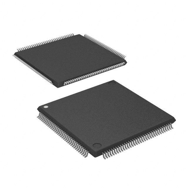
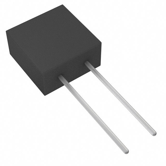
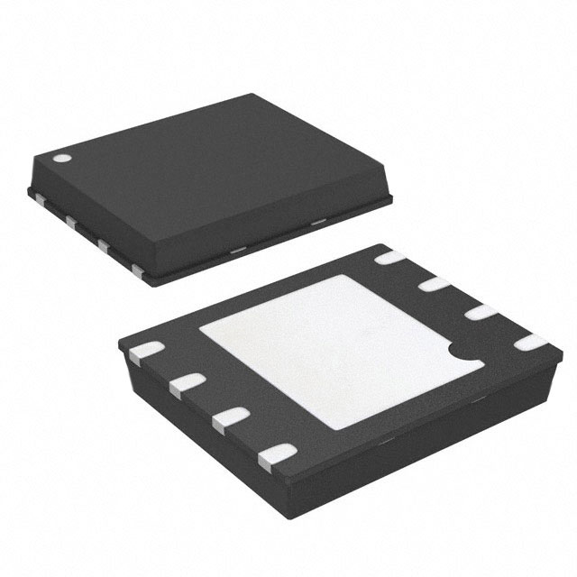
| 产品图片 |
|
| rohs | 符合RoHS无铅 / 符合限制有害物质指令(RoHS)规范要求 |
| 产品系列 | 电源管理 IC,电流和电力监控器、调节器,Maxim Integrated MAX4840EXT+T- |
| 数据手册 | |
| 产品型号 | MAX4840EXT+T |
| 产品 | Power Monitors |
| 产品培训模块 | http://www.digikey.cn/PTM/IndividualPTM.page?site=cn&lang=zhs&ptm=25703http://www.digikey.cn/PTM/IndividualPTM.page?site=cn&lang=zhs&ptm=25705 |
| 产品目录页面 | |
| 产品种类 | 电流和电力监控器、调节器 |
| 供应商器件封装 | SC-70-6 |
| 其它名称 | MAX4840EXT+TDKR |
| 包装 | Digi-Reel® |
| 商标 | Maxim Integrated |
| 安装类型 | 表面贴装 |
| 安装风格 | SMD/SMT |
| 封装 | Reel |
| 封装/外壳 | 6-TSSOP,SC-88,SOT-363 |
| 封装/箱体 | SC-70-6 |
| 工作温度范围 | - 40 C to + 85 C |
| 工厂包装数量 | 2500 |
| 应用 | 手机,数码相机,媒体播放器 |
| 标准包装 | 1 |
| 电源电压-最大 | 28 V |
| 电源电压-最小 | 1.2 V |
| 电源电流 | 240 uA |
| 类型 | 过压保护控制器 |
| 系列 | MAX4840 |
| 输入电压范围 | 1.2 V to 28 V |
| 零件号别名 | MAX4840 |








- 商务部:美国ITC正式对集成电路等产品启动337调查
- 曝三星4nm工艺存在良率问题 高通将骁龙8 Gen1或转产台积电
- 太阳诱电将投资9.5亿元在常州建新厂生产MLCC 预计2023年完工
- 英特尔发布欧洲新工厂建设计划 深化IDM 2.0 战略
- 台积电先进制程称霸业界 有大客户加持明年业绩稳了
- 达到5530亿美元!SIA预计今年全球半导体销售额将创下新高
- 英特尔拟将自动驾驶子公司Mobileye上市 估值或超500亿美元
- 三星加码芯片和SET,合并消费电子和移动部门,撤换高东真等 CEO
- 三星电子宣布重大人事变动 还合并消费电子和移动部门
- 海关总署:前11个月进口集成电路产品价值2.52万亿元 增长14.8%




PDF Datasheet 数据手册内容提取
19-3979; Rev 0; 2/06 Overvoltage-Protection Controllers with Status FLAG General Description Features M The MAX4838A/MAX4840A/MAX4842A are overvoltage- ♦ Overvoltage Protection Up to +28V A protection ICs that protect low-voltage systems against ♦ Preset 7.4V, 5.8V, or 4.7V Overvoltage Trip Level X voltages of up to +28V. If the input voltage exceeds the overvoltage trip level, the MAX4838A/MAX4840A/ ♦ Drives Low-Cost nMOS FET 4 MAX4842A turn off the low-cost external n-channel ♦ Internal 50ms Startup Delay 8 FET(s) to prevent damage to the protected components. ♦ Internal Charge Pump 3 An internal charge pump eliminates the need for external capacitors and drives the FET gate for a simple, ♦ Undervoltage Lockout 8 robust solution. ♦ ±15kV ESD-Protected Input A The MAX4838A has a 7.4V overvoltage threshold, and ♦ Voltage Fault FLAGIndicator /M the MAX4840A has a 5.8V overvoltage threshold. The MAX4842A has a 4.7V overvoltage threshold. The ♦ 6-Pin SC70 and µDFN Packages A MAX4838A/MAX4840A have an undervoltage-lockout ♦ Lead Free X (UVLO) threshold of 3.25V, while the MAX4842A has a UVLO of 2.5V. In addition to the single FET configura- 4 tion, the devices can be configured with back-to-back 8 Ordering Information external FETs to prevent currents from being back-dri- 4 ven into the adapter. PIN- TOP PKG 0 PART On power-up, the device waits for 50ms before driving PACKAGE MARK CODE A GATE high. FLAG is held low for an additional 50ms MAX4838AEXT+T 6 SC70 ACY X6S-1 / after GATE goes high before deasserting. The M MAX4838AELT+ 6 µDFN KU L611-1 MAX4838A/MAX4840A/MAX4842A have an open-drain FLAG output. The FLAG output asserts immediately to MAX4840AEXT+T 6 SC70 ACZ X6S-1 A an overvoltage fault. MAX4840AELT+ 6 µDFN KV L611-1 X Additional features include a ±15kV (HBM) ESD-pro- MAX4842AEXT+T 6 SC70 ADA X6S-1 4 tected input (when bypassed with a 1µF capacitor) and MAX4842AELT+* 6 µDFN KW L611-1 8 a shutdown pin (EN) to turn off the device. Note:All devices specified for the -40°C to +85°C extended 4 All devices are offered in a small 6-pin SC70 and 6-pin temperature range. 2 1.5mm x 1.0mm µDFN packages and are specified *Future product—contact factory for availability. A over the -40°C to +85°C extended temperature range. +Denotes lead-free package. Applications Cell Phones Typical Operating Circuit Digital Still Cameras PDAs and Palmtop Devices INPUT OUTPUT +1.2V TO +28V MP3 Players NMOS 1 4 IN GATE Selector Guide 1µF VIO MAX4838A OV MAX4840A UVLO TRIP EN FLAG MAX4842A PART THRESHOLD 6 3 LEVEL INPUT OUTPUT EN FLAG (V) (V) 2 NOTE: EN AND PULLUP GND RESISTOR MAX4838A 3.25 7.4 Yes Open-Drain MAX4840A 3.25 5.8 Yes Open-Drain MAX4842A 2.50 4.7 Yes Open-Drain Pin Configuration appears at end of data sheet. ________________________________________________________________Maxim Integrated Products 1 For pricing, delivery, and ordering information,please contact Maxim/Dallas Direct!at 1-888-629-4642, or visit Maxim’s website at www.maxim-ic.com.
Overvoltage-Protection Controllers with Status FLAG A ABSOLUTE MAXIMUM RATINGS 2 IN to GND ..............................................................-0.3V to +30V Operating Temperature Range ..........................-40°C to +85°C GATE to GND ........................................................-0.3V to +12V Junction Temperature ....................................................+150°C 4 EN, FLAGto GND ....................................................-0.3V to +6V Storage Temperature Range ............................-65°C to +150°C 8 Continuous Power Dissipation (TA= +70°C) Lead Temperature (soldering, 10s) ................................+300°C 4 6-Pin SC70 (derate 3.1mW/°C above +70°C) .............245mW 6-Pin µDFN (derate 2.1mW/°C above +70°C) ............477mW X A Stresses beyond those listed under “Absolute Maximum Ratings” may cause permanent damage to the device. These are stress ratings only, and functional M operation of the device at these or any other conditions beyond those indicated in the operational sections of the specifications is not implied. Exposure to absolute maximum rating conditions for extended periods may affect device reliability. / A 0 ELECTRICAL CHARACTERISTICS 4 8 (VIN= +5V (MAX4838A/MAX4840A), VIN= +4V (MAX4842A), TA= -40°C to +85°C, unless otherwise noted. Typical values are at TA = +25°C.) (Note 1) 4 PARAMETER SYMBOL CONDITIONS MIN TYP MAX UNITS X A Input Voltage Range VIN 1.2 28.0 V MAX4838A/MAX4840A 3.0 3.25 3.5 M Undervoltage-Lockout Threshold UVLO VIN falling V MAX4842A 2.3 2.5 2.7 A/ Undervoltage-Lockout Hysteresis 50 mV 8 VIN rising MAX4838A 7.0 7.4 7.8 3 Overvoltage Trip Level OVLO VIN rising MAX4840A 5.5 5.8 6.1 V VIN rising MAX4842A 4.4 4.7 5.0 8 MAX4838A 100 4 Overvoltage Trip Level Hysteresis MAX4840A 80 mV X MAX4842A 50 A No load, EN = GND or 5V, 80 200 M VIN = 5V (MAX4838A/MAX4840A) IN Supply Current IIN µA No load, EN = GND or 4.0V, 75 160 VIN = 4V (MAX4842A) VIN = 2.9V (MAX4838A/MAX4840A) 30 UVLO Supply Current IUVLO µA VIN = 2.2V (MAX4842A) 22 MAX4838A/MAX4840A 9 10 GATE Voltage VGATE IGATE sourcing 1µA V MAX4842A 7.5 8.0 GATE Pulldown Current IPD VIN > VOVLO, VGATE = 5.5V 27 mA 1.2V ≤ VIN < UVLO, 0.4 ISINK = 50µA FLAG Output Low Voltage VOL FLAG asserted V VIN ≥ OVLO, ISINK = 0.4 1mA FLAG Output High Leakage IOH VFLAG = 5.5V, FLAG deasserted 1 µA EN Input High Voltage VIH 1.5 V EN Input Low Voltage VIL 0.4 V EN Input Leakage ILKG EN = GND or 5.5V 1 µA 2 _______________________________________________________________________________________
Overvoltage-Protection Controllers with Status FLAG ELECTRICAL CHARACTERISTICS (continued) M (VIN= +5V (MAX4838A/MAX4840A), VIN= +4V (MAX4842A), TA= -40°C to +85°C, unless otherwise noted. Typical values are at TA A = +25°C.) (Note 1) X PARAMETER SYMBOL CONDITIONS MIN TYP MAX UNITS 4 TIMING 8 Startup Delay tSTART VIN > VUVLO, VGATE > 0.3V, Figure 1 20 50 80 ms 3 FLAG Blanking Time tBLANK VGATE > 0.3V, VFLAG > 2.4V, Figure 1 20 50 80 ms 8 VG A TE = 0.3V to 8V ( MA X 4838A/MA X4 840A), A GATE Turn-On Time tGON VG A TE = 0.3V to 6V ( MA X 4842A), 10 ms / CG A TE = 1500pF , Fig u re 1 M VIN increasing from 5V to 8V at 3V/µs A GATE Turn-Off Time tGOFF (MAX4838A/MAX4840A), VIN increasing 6 20 µs X from 4V to 6V at 3V/µs (MAX4842A), VGATE = 0.3V, CGATE = 1500pF, Figure 2 4 8 VIN increasing from 5V to 8V at 3V/µs 4 (MAX4838A/MAX4840A), VIN increasing FLAG Assertion Delay tFLAG 5.8 µs 0 from 4V to 6V at 3V/µs (MAX4842A), A VFLAG = 0.4V, Figure 2 / VIN increasing from 0 to 8V M Initial Overvoltage Fault Delay tOVP (MAX4838A/MAX4840A), VIN increasing 1.5 µs A from 0V to 6V (MAX4842A), IGATE = 80% of IPD, Figure 3 X 4 Disable Time tDIS VE N = 2.4V , VG A TE = 0.3V , Fig ure 4 2 µs 8 Note 1: All parts are 100% tested at +25°C. Electrical limits across the full temperature range are guaranteed by design and 4 correlation. 2 A Typical Operating Characteristics (VIN= +5V (MAX4838A/MAX4840A), VIN= +4V (MAX4842A); Si9936DY external MOSFET in back-to-back configuration; TA= +25°C, unless otherwise noted.) REVERSE CURRENT MAX4838A/MAX4840A SUPPLY CURRENT vs. INPUT VOLTAGE vs. OUTPUT VOLTAGE GATE VOLTAGE vs. INPUT VOLTAGE 560000 MAX4838A toc01 1000 SINGLE MOSFET MAX4838A toc02 12 MAX4838A toc03 µSUPPLY CURRENT (A) 234000000 µREVERSE CURRENT (A) 110100 BACK-TO-BACK MOSFETS GATE VOLTAGE (V) 369 MAX4840A MAX4838A 100 0 0.1 0 0 5 10 15 20 25 30 3.5 4.0 4.5 5.0 5.5 3 4 5 6 7 8 INPUT VOLTAGE (V) OUTPUT VOLTAGE (V) INPUT VOLTAGE (V) _______________________________________________________________________________________ 3
Overvoltage-Protection Controllers with Status FLAG A Typical Operating Characteristics (continued) 2 (VIN= +5V (MAX4838A/MAX4840A), VIN= +4V (MAX4842A); Si9936DY external MOSFET in back-to-back configuration; TA= +25°C, unless otherwise noted.) 4 8 MAX4842A MAX4838A/MAX4840A 4 GATE VOLTAGE vs. INPUT VOLTAGE GATE VOLTAGE vs. INPUT VOLTAGE POWER-UP RESPONSE AX 12 MAX4838A toc04 11.0 IGATE = 0 MAX4838A toc05 50VV MAX4838A toc06 IN M 9 10.5 / GE (V) MAX4842A GE (V) IGATE = 4µA 10V GATE A OLTA 6 OLTA 10.0 IGATE = 8µA 0V 40 GATE V GATE V 5V OUT 8 3 9.5 0V 4 5V ROUT = ∞ FLAG COUT = 0 X 0 9.0 A 0 1 2 3 4 5 6 7 8 5.0 5.1 5.2 5.3 5.4 5.5 20ms/div INPUT VOLTAGE (V) INPUT VOLTAGE (V) M / MAX4838A/MAX4840A MAX4842A MAX4842A A POWER-UP RESPONSE POWER-UP RESPONSE POWER-UP RESPONSE 8 MAX4838A toc07 MAX4838A toc08 MAX4838A toc09 3 5V 4V 4V 8 IN IN IN 0V 0V 0V 4 8V 8V X 10V GATE GATE GATE A 0V 0V 0V 1A M 4V 800mA IIN OUT IIN 0A 0V 0A 4V 4V 5V ROUT = 5Ω 0V ROUT = ∞ FLAG 0V ROUT = 5Ω FLAG FLAG COUT = 0 0V 20ms/div 20ms/div 20ms/div OVERVOLTAGE RESPONSE POWER-UP OVERVOLTAGE RESPONSE POWER-DOWN RESPONSE MAX4838A toc10 MAX4838A toc11 MAX4838A toc12 8V IN 5V RLOAD = 50Ω 5V 8V IN RFLAG = 100kΩ TO +5V IN 10V 0V GATE PULLED UP 0V TO IN WITH 100Ω 0V GATE 5V 10V GATE GATE 40mA 0V 0V 50mA 5V IGATE OUT 0A IGATE 0A 0V 5V 5V 5V 0V CGATE = 1500pF FLAG 0V FLAG FLAG 0V 400ns/div 1µs/div 10ms/div 4 _______________________________________________________________________________________
Overvoltage-Protection Controllers with Status FLAG Pin Description M PIN NAME FUNCTION A Input. IN is both the power-supply input and the overvoltage sense input. Bypass IN to GND with X 1 IN a 1µF capacitor or larger. 4 2 GND Ground 8 Fault Indication Output, Open-Drain, Active Low. FLAG is asserted low during undervoltage- 3 3 FLAG lockout and overvoltage-lockout conditions. FLAG is deasserted during normal operation. 8 Gate-Drive Output. GATE is the output of an on-chip charge pump. When VUVLO < VIN < VOVLO, A 4 GATE GATE is driven high to turn on the external n-channel MOSFET(s). / M No Connection. Not internally connected for µDFN package. Connected to ground for SC70 5 N.C. 6-pin package; connect to ground or leave unconnected. A X Device Enable Input, Active Low. Drive EN low or connect to ground to allow normal device 6 EN operation. Drive EN high to turn off the external MOSFET. 4 8 4 0 Timing Diagrams A / M 5V (4V) 8V (6V) VIN VUVLO VIN VOVLO A 0V tGON 5V (4V) tFLAG X tGOFF 8V (6V) 4 tSTART 8 VGATE VGATE 0.3V 0.3V 4 tBLANK 2 2.4V VFLAG VFLAG A 0.4V ( ) MAX4842A ( ) MAX4842A Figure 1. Startup Timing Diagram Figure 2. Shutdown Timing Diagram 8V (6V) VIN VOVLO VEN 1.5V 0V tOVP tDIS 80% VGATE IGATE 0.3V ( ) MAX4842A Figure 3. Power-Up Overvoltage Timing Diagram Figure 4. Disable Timing Diagram _______________________________________________________________________________________ 5
Overvoltage-Protection Controllers with Status FLAG A 2 4 5.5V 2x CHARGE 8 IN GATE DRIVER GATE REGULATOR PUMP 4 GND X UVLO AND A OVLO DETECTOR CONTROL M LOGIC AND TIMER FLAG EN / MAX4838A A MAX4840A MAX4842A 0 4 Figure 5. Functional Diagram 8 4 X Detailed Description GATE Driver An on-chip charge pump is used to drive GATE above A The MAX4838A/MAX4840A/MAX4842A provide up to IN, allowing the use of low-cost n-channel MOSFETS. +28V overvoltage protection for low-voltage systems. M The charge pump operates from the internal 5.5V When the input voltage exceeds the overvoltage trip level, regulator. / the MAX4838A/MAX4840A/MAX4842A turn off a low-cost A external n-channel FET(s) to prevent damage to the pro- The actual GATE output voltage tracks approximately 8 tected components. An internal charge pump (Figure 5) two times VIN until VIN exceeds 5.5V or the OVLO trip 3 drives the FET gate for a simple, robust solution. level is exceeded, whichever comes first. The MAX4838A has a 7.4V typical OVLO; therefore GATE 8 Undervoltage Lockout (UVLO) remains relatively constant at approximately 10.5V for 4 The MAX4838A/MAX4840A have a fixed 3.25V typical 5.5V < VIN < 7.4V. The MAX4840A has a 5.8V typical X undervoltage-lockout level (UVLO) while the MAX4842A OVLO, but this can be as low as 5.5V. The MAX4840A A has a 2.5V typical UVLO. When VIN is less than the in practice may never actually achieve the full 10.5V UVLO, the GATE driver is held low and FLAGis asserted. GATE output. The MAX4842A has a 4.7V (typ) OVLO, M and the GATE output voltage is 2x the input voltage. Overvoltage Lockout (OVLO) The GATE output voltage as a function of input voltage The MAX4838A has a 7.4V typical overvoltage threshold is shown in the Typical Operating Characteristics. (OVLO), and the MAX4840A has a 5.8V typical overvolt- age threshold. The MAX4842A has a 4.7V typical over- Device Operation voltage threshold. When VIN is greater than OVLO, the The MAX4838A/MAX4840A/MAX4842A have an on- GATE driver is held low and FLAGis asserted. board state machine to control device operation. A flowchart is shown in Figure 6. On initial power-up, if FLAGOutput VIN < UVLO or if VIN > OVLO, GATE is held at 0V, and The FLAG output is used to signal the host system FLAGis low. there is a fault with the input voltage. FLAG asserts immediately to an overvoltage fault. FLAG is held low If UVLO < VIN< OVLO and ENis low, the device enters for 50ms after GATE turns on before deasserting. startup after a 50ms internal delay. The internal charge pump is enabled, and GATE begins to be driven above All devices have an open-drain FLAG output. Connect VINby the internal charge pump. FLAGis held low dur- a pullup resistor from FLAG to the logic I/O voltage of ing startup until the FLAGblanking period expires, typi- the host system. cally 50ms after the GATE starts going high. At this ENEnable Input point the device is in its on state. EN is an active-low enable input. Drive EN low or con- At any time if VIN drops below UVLO, FLAG is driven nect to ground to enable normal device operation. low and GATE is driven to ground. Drive EN high to force the external MOSFET(s) off. EN does not override an OVLO or UVLO fault. 6 _______________________________________________________________________________________
Overvoltage-Protection Controllers with Status FLAG M NMOS OUTPUT STANDBY INPUT A GATE = 0 0 TO 28V FLAG = LOW X VIN > UVLO 1 IN GATE 4 4 8 1µF VIN < UVLO TIMCOEUR NSTTIANRGTS MAX4838A VIO 3 MAX4840A 8 6 MAX4842A A t = 50ms EN 3 FLAG / 2 M OVLO CHECK GND NOTE: EN AND PULLUP GATE = 0 RESISTOR ON MAX4838A/ A FLAG = LOW MAX4840A/MAX4842A ONLY. X VIN < OVLO Figure 7. Back-to-Back External MOSFET Configuration 4 VIN > OVLO STARTUP 8 GATE DRIVEN HIGH FLAG = LOW 3.5V, consider using a MOSFET specified for a lower 4 VGS voltage. Also, the VDS should be 30V for the MOS- 0 t = 50ms FET to withstand the full 28V IN range of all devices. A Table 1 shows a selection of MOSFETs appropriate for ON use with the MAX4838A/MAX4840A/MAX4842A. / GATE HIGH M FLAG = HIGH IN Bypass Considerations A For most applications, bypass IN to GND with a 1µF X ceramic capacitor. If the power source has significant Figure 6. State Diagram inductance due to long lead length, take care to pre- 4 Applications Information vent overshoots due to the LC tank circuit and provide 8 protection if necessary to prevent exceeding the 30V 4 MOSFET Configuration absolute maximum rating on IN. 2 The MAX4838A/MAX4840A/MAX4842A can be used The MAX4838A/MAX4840A/MAX4842A provide protec- with either a single MOSFET configuration as shown in A tion against voltage faults up to 28V, but this does not the Typical Operating Circuit, or can be configured with include negative voltages. If negative voltages are a con- a back-to-back MOSFET as shown in Figure 7. The cern, connect a Schottky diode from IN to GND to clamp back-to-back configuration has almost zero reverse negative input voltages. current when the input supply is below the output. ESD Test Conditions If reverse current leakage is not a concern, a single MOSFET can be used. This approach has half the loss ESD performance depends on a number of conditions. of the back-to-back configuration when used with simi- The MAX4838A/MAX4840A/MAX4842A are specified lar MOSFET types, and is a lower cost solution. Note for ±15kV typical ESD resistance on IN when IN is that if the input is actually pulled low, the output is bypassed to ground with a 1µF ceramic capacitor. pulled low as well due to the parasitic body diode in the Contact Maxim for a reliability report that documents MOSFET. If this is a concern, then the back-to-back test setup, methodology, and results. configuration should be used. Human Body Model MOSFET Selection Figure 8 shows the Human Body Model, and Figure 9 The MAX4838A/MAX4840A/MAX4842A are designed for shows the current waveform it generates when dis- use with either a single n-channel MOSFET or dual back- charged into a low impedance. This model consists of to-back n-channel MOSFETs. In most situations, a 100pF capacitor charged to the ESD voltage of inter- MOSFETs with RDS(ON) specified for a VGSof 4.5V work est, which is then discharged into the device through a well. If the input supply is near the UVLO maximum of 1.5kΩresistor. _______________________________________________________________________________________ 7
Overvoltage-Protection Controllers with Status FLAG A Table 1. MOSFET Suggestions 2 CONFIGURATION/ RON AT 4.5V 4 PART PACKAGE VDS MAX (V) (mΩ) MANUFACTURER 8 Si5902DC Dual/1206-8 30 143 Vishay Silconix 4 www.vishay.com X Si1426DH Single/SC70-6 30 115 402-563-6866 A FDC6305N Dual/SSOT-6 20 80 Fairchild Semiconductor M FDC6561AN Dual/ SSOT-6 30 145 www.fairchildsemi.com FDG315N Single/SC70-6 30 160 207-775-8100 / A IEC 61000-4-2 the ESD-withstand voltage measured to this standard is 0 Since January 1996, all equipment manufactured and/or generally lower than that measured using the Human 4 sold in the European community has been required to Body Model. Figure 11 shows the current waveform for 8 meet the stringent IEC 61000-4-2 specification. The IEC the ±8kV IEC 61000-4-2 Level 4 ESD Contact 4 61000-4-2 standard covers ESD testing and perfor- Discharge test. The Air-Gap test involves approaching X mance of finished equipment; it does not specifically the device with a charger probe. The Contact refer to integrated circuits. The MAX4838A/MAX4840A/ Discharge method connects the probe to the device A MAX4842A help users design equipment that meets before the probe is energized. M Level 3 of IEC 61000-4-2, without additional ESD-protec- tion components. / A The main difference between tests done using the 8 Human Body Model and IEC 61000-4-2 is higher peak current in IEC 61000-4-2. Because series resistance is 3 lower in the IEC 61000-4-2 ESD test model (Figure 10), 8 4 X A M RC RD 1MΩ 1.5kΩ IP 100% Ir PEAK-TO-PEAK RINGING CHARGE-CURRENT- DISCHARGE 90% (NOT DRAWN TO SCALE) LIMIT RESISTOR RESISTANCE AMPERES HIGH- DEVICE VOLTAGE Cs STORAGE UNDER 36.8% DC 100pF CAPACITOR TEST SOURCE 10% 0 0 TIME tRL tDL CURRENT WAVEFORM Figure 8. Human Body ESD Test Model Figure 9. Human Body Model Current Waveform 8 _______________________________________________________________________________________
Overvoltage-Protection Controllers with Status FLAG M I 100% A 50Ω RtoC 1 00Ω 33R0DΩ 90% X 4 CHARGE-CURRENT- DISCHARGE LIMIT RESISTOR RESISTANCE PEAK 8 I 3 HIGH- DEVICE 8 VOLTAGE Cs STORAGE UNDER DC 150pF CAPACITOR TEST A SOURCE / M 10% A tr = 0.7ns to 1ns t X 30ns 60ns 4 8 Figure 10. IEC 61000-4-2 ESD Test Model Figure 11. IEC 61000-4-2 ESD Generator Current 4 0 A Pin Configurations Chip Information / M PROCESS: BiCMOS A TOP VIEW X + 4 IN 1 6 EN 8 MAX4838A 4 GND 2 MAX4840A 5 N.C. 2 MAX4842A A FLAG 3 4 GATE SC70 TOP VIEW + IN 1 6 EN MAX4838A GND 2 MAX4840A 5 N.C. MAX4842A FLAG 3 4 GATE µDFN _______________________________________________________________________________________ 9
Overvoltage-Protection Controllers with Status FLAG A Package Information 2 (The package drawing(s) in this data sheet may not reflect the most current specifications. For the latest package outline information go to www.maxim-ic.com/packages.) 4 8 S 4 EP N. X DF U L A 6 M / A 0 4 8 4 X A M / A 8 3 8 4 X A TABLE 1 (cid:31)(cid:31) (cid:31)(cid:31)T r(cid:31)anslation Table for Calendar Year Code Calendar Year 2005 2006 2007 2008 2009 2010 2011 2012 2013 2014 M Legend: Marked with bar Blank space - no bar required TABLE 2 (cid:31)(cid:31) (cid:31)(cid:31)T r(cid:31)anslation Table for Payweek Binary Coding Payweek 06-11 12-17 18-23 24-29 30-35 36-41 42-47 48-51 52-05 Legend: Marked with bar Blank space - no bar required TITLE: PACKAGE OUTLINE, 6L uDFN, 1.5x1.0x0.8mm -DRAWING NOT TO SCALE- APPROVAL DOCUM2EN1T C-O0NTR1O4L N7O. REDV. 22 10 ______________________________________________________________________________________
Overvoltage-Protection Controllers with Status FLAG Package Information (continued) M (The package drawing(s) in this data sheet may not reflect the most current specifications. For the latest package outline information A go to www.maxim-ic.com/packages.) X 4 S P L.E 8 6 0, 3 7 C S 8 A / M A X 4 8 4 0 A / M A X 4 8 4 2 A PACKAGE OUTLINE, 6L SC70 1 21-0077 C 1 Maxim cannot assume responsibility for use of any circuitry other than circuitry entirely embodied in a Maxim product. No circuit patent licenses are implied. Maxim reserves the right to change the circuitry and specifications without notice at any time. Maxim Integrated Products, 120 San Gabriel Drive, Sunnyvale, CA 94086 408-737-7600 ____________________11 © 2006 Maxim Integrated Products Printed USA is a registered trademark of Maxim Integrated Products, Inc.