ICGOO在线商城 > 集成电路(IC) > 线性 - 放大器 - 仪表,运算放大器,缓冲器放大器 > MAX4378TAUD+

 Datasheet下载
- 型号: MAX4378TAUD+
- 制造商: Maxim
- 库位|库存: xxxx|xxxx
- 要求:
| 数量阶梯 | 香港交货 | 国内含税 |
| +xxxx | $xxxx | ¥xxxx |
查看当月历史价格
查看今年历史价格
MAX4378TAUD+产品简介:
ICGOO电子元器件商城为您提供MAX4378TAUD+由Maxim设计生产,在icgoo商城现货销售,并且可以通过原厂、代理商等渠道进行代购。 MAX4378TAUD+价格参考。MaximMAX4378TAUD+封装/规格:线性 - 放大器 - 仪表,运算放大器,缓冲器放大器, 电流检测 放大器 4 电路 14-TSSOP。您可以下载MAX4378TAUD+参考资料、Datasheet数据手册功能说明书,资料中有MAX4378TAUD+ 详细功能的应用电路图电压和使用方法及教程。
Maxim Integrated的MAX4378TAUD+是一款高精度电流检测放大器,属于线性放大器中的仪表放大器类别。该器件主要用于需要高精度测量电流的应用场景,广泛应用于工业控制、电源管理、电池供电设备以及电机控制系统等领域。

MAX4378TAUD+具备宽输入共模电压范围(-0.1V至+28V),能够适应多种电源系统环境,适用于高压侧或低压侧电流监测。其高带宽(典型值为500kHz)和快速响应时间使其适合用于动态负载监控和实时反馈控制。

该芯片采用小型10引脚TDFN封装,节省电路板空间,适合紧凑型设计。由于其高集成度和稳定性,MAX4378TAUD+常被用于电动汽车充电系统、DC-DC转换器、服务器电源、通信设备电源监控等对精度与可靠性要求较高的场合。

此外,它还支持宽温度范围(-40°C至+125°C),适用于严苛工业环境下的稳定运行。
| 参数 | 数值 |
| -3db带宽 | 2MHz |
| 产品目录 | 集成电路 (IC)半导体 |
| 描述 | IC OPAMP CURR SENSE 2MHZ 14TSSOP电流灵敏放大器 High-Side Current-Sense Amp |
| 产品分类 | Linear - Amplifiers - Instrumentation, OP Amps, Buffer Amps集成电路 - IC |
| 品牌 | Maxim Integrated |
| 产品手册 | |
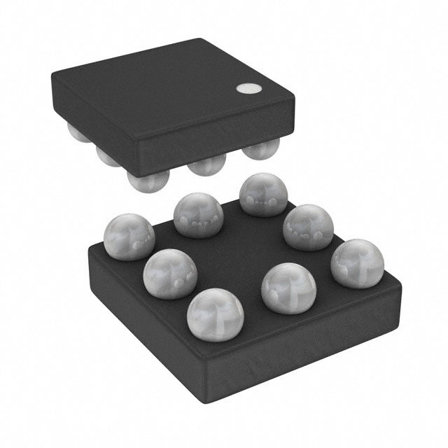
| 产品图片 |
|
| rohs | 符合RoHS无铅 / 符合限制有害物质指令(RoHS)规范要求 |
| 产品系列 | 放大器 IC,电流灵敏放大器,Maxim Integrated MAX4378TAUD+- |
| 数据手册 | |
| 产品型号 | MAX4378TAUD+ |
| 产品培训模块 | http://www.digikey.cn/PTM/IndividualPTM.page?site=cn&lang=zhs&ptm=25703http://www.digikey.cn/PTM/IndividualPTM.page?site=cn&lang=zhs&ptm=25705 |
| 产品目录页面 | |
| 产品种类 | 电流灵敏放大器 |
| 供应商器件封装 | 14-TSSOP |
| 共模抑制比—最小值 | 90 dB |
| 其它有关文件 | |
| 包装 | 管件 |
| 压摆率 | 10 V/µs |
| 商标 | Maxim Integrated |
| 增益带宽积 | - |
| 安装类型 | 表面贴装 |
| 安装风格 | SMD/SMT |
| 封装 | Tube |
| 封装/外壳 | 14-TSSOP(0.173",4.40mm 宽) |
| 封装/箱体 | TSSOP-14 |
| 工作温度 | -40°C ~ 125°C |
| 工厂包装数量 | 96 |
| 应用说明 | |
| 放大器类型 | 电流检测 |
| 最大工作温度 | + 125 C |
| 最小工作温度 | - 40 C |
| 标准包装 | 1 |
| 电压-电源,单/双 (±) | 3 V ~ 28 V |
| 电压-输入失调 | - |
| 电流-电源 | 1mA |
| 电流-输入偏置 | 800µA |
| 电流-输出/通道 | - |
| 电源电压-最大 | 28 V |
| 电源电压-最小 | 3 V |
| 电源电流 | 1 mA |
| 电路数 | 4 |
| 系列 | MAX4378T |
| 输出电流 | 2 mA |
| 输出类型 | - |
| 零件号别名 | MAX4378T |


- 商务部:美国ITC正式对集成电路等产品启动337调查
- 曝三星4nm工艺存在良率问题 高通将骁龙8 Gen1或转产台积电
- 太阳诱电将投资9.5亿元在常州建新厂生产MLCC 预计2023年完工
- 英特尔发布欧洲新工厂建设计划 深化IDM 2.0 战略
- 台积电先进制程称霸业界 有大客户加持明年业绩稳了
- 达到5530亿美元!SIA预计今年全球半导体销售额将创下新高
- 英特尔拟将自动驾驶子公司Mobileye上市 估值或超500亿美元
- 三星加码芯片和SET,合并消费电子和移动部门,撤换高东真等 CEO
- 三星电子宣布重大人事变动 还合并消费电子和移动部门
- 海关总署:前11个月进口集成电路产品价值2.52万亿元 增长14.8%


PDF Datasheet 数据手册内容提取
Click here for production status of specific part numbers. MAX4376/MAX4377/ Single/Dual/Quad, High-Side MAX4378 Current-Sense Amplifiers with Internal Gain General Description Features The MAX4376/MAX4377/MAX4378 single, dual, and ● Low-Cost, Single/Dual/Quad, High-Side Current- quad precision high-side current-sense amplifiers are Sense Amplifiers available in space-saving packages. They feature ● ±0.5% Typical Full-Scale Accuracy buffered voltage outputs that eliminate the need for ● +3V to +28V Supply Operation gain-setting resistors and are ideal for today’s notebook ● Adjustable Current-Sense Capability with External computers, cell phones, and other systems where Sense Resistor current monitoring is critical. These precision devices are ● Buffered Output Voltage with 2mA Drive offered in three fixed-gain versions of 20, 50, and 100: ● 1mA (typ) Supply Current GAIN SUFFIX ● 2.0MHz Bandwidth (Gain = +20V/V) 20 T ● Automotive Temperature Range (-40°C to +125°C) 50 F ● High Accuracy +2V to +28V Common-Mode Range, 100 H Functional Down to 0V, Independent of Supply Voltage For example, MAX4376TAUK is a single high-side amplifier ● Three Gain Versions Available with a gain of 20. +20V/V (MAX437_T) +50V/V (MAX437_F) High-side current monitoring is especially useful in +100V/V (MAX437_H) battery-powered systems since it does not interfere with the ground path of the battery charger. The input ● Available in Space-Saving 5-Pin SOT23 (Single), 8-Pin µMAX (Dual), and 14-Pin TSSOP (Quad) common-mode range of 0 to +28V is independent of the supply voltage and ensures that the current-sense ● AEC-Q100 Qualified, Refer to Ordering Information for the List of /V Parts feedback remains viable even when connected to a battery pack in deep discharge. Applications The full-scale current reading can be set by choosing the appropriate voltage gain and external-sense resistor. This ● Notebook Computers capability offers a high level of integration and flexibility, ● Current-Limited Power Supplies resulting in a simple and compact current-sense solution. ● Fuel Gauges in PC The MAX4376/MAX4377/MAX4378 operate over a supply ● General-System/Board-Level Current Monitoring voltage range of +3V to +28V, draw 1mA of supply current ● Battery Chargers per amplifier, and operate over the full automotive tempera- ● Portable/Battery-Powered Systems ture range of -40°C to +125°C. These devices have a wide ● Cell Phones bandwidth of 2MHz, making them suitable for use inside battery-charger control loops. The buffered outputs drive ● Smart Battery Packages up to 2mA of output current into a ground-referenced load. ● Automotive Current Detect The MAX4376 is available in a tiny 5-pin SOT23 package. ● Power Management Systems The MAX4377/MAX4378 are available in space-saving ● PA Bias Control 8-pin µMAX® and 14-pin TSSOP packages, respectively. ● Automotive Typical Operating Circuit 0 TO +28V VSENSE ILOAD RSENSE +3V TO +28V RS+ RS- VCC 0.1µF MAX4376T/F/H A/D LOAD/ OUT CONVERTER BATTERY µMAX is a registered trademark of Maxim Integrated Products, Inc. GND 19-1781; Rev 13; 11/19
MAX4376/MAX4377/ Single/Dual/Quad, High-Side MAX4378 Current-Sense Amplifiers with Internal Gain Absolute Maximum Ratings VCC, RS+, RS- to GND .........................................-0.3V to +30V 8-Pin SO (derate 5.88mW/°C above +70°C) ...............471mW OUT to GND .............................................-0.3V to (VCC + 0.3V) 14-Pin SO (derate 8.33mW/°C above +70°C) .............667mW Differential Input Voltage (VRS+ - VRS- ) ...............................±8V 14-Pin TSSOP (derate 9.1mW/°C above +70°C) ........727mW Output Short Circuit to VCC .......................................Continuous Operating Temperature Range .........................-40°C to +125°C Output Short Circuit to GND....................................................1s Junction Temperature ......................................................+150°C Current into Any Pin .........................................................±20mA Storage Temperature Range ............................-65°C to +150°C Continuous Power Dissipation (TA = +70°C) Lead Temperature (soldering, 10s) .................................+300°C 5-Pin SOT23 (derate 3.10mW/°C above +70°C) ...246.70mW Soldering Temperature (reflow) .......................................+260°C 8-Pin µMAX (derate 4.5mW/°C above +70°C) ............362mW Stresses beyond those listed under “Absolute Maximum Ratings” may cause permanent damage to the device. These are stress ratings only, and functional operation of the device at these or any other conditions beyond those indicated in the operational sections of the specifications is not implied. Exposure to absolute maximum rating conditions for extended periods may affect device reliability. Package Information 5 SOT23 PACKAGE CODE U5+2, U5+2A Outline Number 21-0057 Land Pattern Number 90-0174 Thermal Resistance, Multi-Layer Board: Junction to Ambient (θJA) 255.90°C/W Junction to Case (θJC) 81°C/W For the latest package outline information and land patterns (footprints), go to www.maximintegrated.com/packages. Note that a “+”, “#”, or “-” in the package code indicates RoHS status only. Package drawings may show a different suffix character, but the drawing pertains to the package regardless of RoHS status. Package thermal resistances were obtained using the method described in JEDEC specification JESD51-7, using a four-layer board. For detailed information on package thermal considerations, refer to www.maximintegrated.com/thermal-tutorial. www.maximintegrated.com Maxim Integrated │ 2
MAX4376/MAX4377/ Single/Dual/Quad, High-Side MAX4378 Current-Sense Amplifiers with Internal Gain Electrical Characteristics (VRS+ = 0 to 28V, VSENSE = (VRS+ - VRS- ) = 0V, VCC = +3.0V to +28V, RL = ∞, TA = TMIN to TMAX, unless otherwise noted. Typical values are at TA = +25°C.) (Note 1) PARAMETER SYMBOL CONDITIONS MIN TYP MAX UNITS Operating Voltage Range VCC Guaranteed by PSR test 3 28 V Common-Mode Input Range VCM Guaranteed by total OUT voltage error test 0 28 V Common-Mode Rejection CMR 2V ≤ VRS+ ≤ 28V, VSENSE = 100mV 90 dB Supply Current per Amplifier ICC VSENSE = 5mV, VRS+ > 2.0V, VCC = 12V 1 2.2 mA Leakage Current IRS+, IRS- VCC = 0V, VRS+ = 28V 8 mA VRS+ > 2.0V 0 60 IRS+ VRS+ ≤ 2.0V -400 +60 Input Bias Current mA VRS+ > 2.0V 0 120 IRS- VRS+ ≤ 2.0V -800 +120 Full-Scale Sense Voltage VSENSE 150 mV VSENSE = 100mV, ±6.75 VCC = 12V, VRS+ = 12V VSENSE = 100mV, VCC = 12V, TA = +25°C, ±0.5 ±3.25 VRS+ = 12V VSENSE = 100mV, ±11 VCC = 28V, VRS+ = 28V Total OUT Voltage Error (Note 2) IOUT ≤ 2mA VSENSE = 100mV, % VCC = 28V, VRS+ = 28V, ±0.5 ±5 TA = +25°C VSENSE = 100mV, ±9 ±32 VCC = 12V, VRS+ = 0.1V VSENSE = 6.25mV, VCC = 12V, VRS+ = 12V ±7 (Note 3) OUT High Voltage (Note 4) (VCC - VOUT) VCC = 3V, IOUT = 2mA, VRS+ = 28V 0.9 1.2 V IOUT = 200µA, VCC = VRS+ = 12V, OUT Low Voltage VOL 25 40 mV VSENSE = 0V, TA = +25°C www.maximintegrated.com Maxim Integrated │ 3
MAX4376/MAX4377/ Single/Dual/Quad, High-Side MAX4378 Current-Sense Amplifiers with Internal Gain Electrical Characteristics (continued) (VRS+ = 0 to 28V, VSENSE = (VRS+ - VRS- ) = 0V, VCC = +3.0V to +28V, RL = ∞, TA = TMIN to TMAX, unless otherwise noted. Typical values are at TA = +25°C.) (Note 1) PARAMETER SYMBOL CONDITIONS MIN TYP MAX UNITS VSENSE = 100mV 2 (gain = +20V/V) VCC = 12V VSENSE = 100mV 1.7 Bandwidth BW VRS+ = 12V (gain = +50V/V) MHz VSENSE = 15pF VSENSE = 100mV 1.2 (gain = +100V/V) VSENSE = 6.25mV (Note 3) 0.5 Slew Rate SR VSENSE = 20mV to 100mV, CLOAD = 15pF 10 V/µs MAX437_T +20 Gain AV MAX437_F +50 V/V MAX437_H +100 VSENSE = 10mV to TA = TMIN to TMAX ±5.5 150mV, VCC = 12V, IOUT = 2mA, gain = 20 and 50, VRS+ = 12V TA = +25°C ±0.5 ±2.5 Gain Accuracy DAV % VSENSE = 10mV to TA = TMIN to TMAX 5.5 150mV, VCC = 20V, IOUT = 2mA, gain = 100, VRS+ = 12V TA = +25°C ±0.5 ±2.5 VSENSE = 6.25mV 400 OUT Setting Time to 1% of VCC = 12V, VRS+ = 12V, to 100mV ns Final Value CLOAD = 15pF VSENSE = 100mV 800 to 6.25mV Maximum Capacitive Load CLOAD No sustained oscillation 1000 pF Output Resistance ROUT VSENSE = 100mV 5 W Power-Supply Rejection PSR VRS+ > 2V, VOUT = 1.6V, VCC = 3V to 28V 66 90 dB Power-Up Time to 1% of Final VSENSE = 100mV, CLOAD = 15pF 2 µs Value Saturation Recovery Time to VCC = 12V, VRS+ = 12V, CLOAD = 15pF, 1 µs 1% of Final Value VSENSE = 100mV Reverse Recovery Time to 1% VCC = 12V, VRS_ = 12V, CLOAD = 15pF, 1 µs of Final Value VSENSE = -100mV to +100mV Note 1: All devices are 100% production tested at TA = +25°C. All temperature limits are guaranteed by design. Note 2: Total OUT Voltage Error is the sum of gain and offset errors. Note 3: 6.25mV = 1/16 of 100mV full-scale sense voltage. Note 4: VSENSE such that VOUT is in saturation. www.maximintegrated.com Maxim Integrated │ 4
MAX4376/MAX4377/ Single/Dual/Quad, High-Side MAX4378 Current-Sense Amplifiers with Internal Gain Typical Operating Characteristics (VCC = VRS+ = 12V, VSENSE = 100mV, TA = +25°C.) SUPPLY CURRENT (PER AMPLIFIER) SUPPLY CURRENT (PER AMPLIFIER) TOTAL OUTPUT ERROR vs. SUPPLY VOLTAGE vs. TEMPERATURE vs. SUPPLY VOLTAGE (VSENSE = 100mV) SUPPLY CURRENT (mA)000000001.........667788990500505050 MAX4376H MAX4376MMTAAXX44337766FF MAX4376/7/8 toc01 SUPPLY CURRENT (mA) 000111......486204 MAX4376HMAX4376TMAX4376F MAX4376/7/8 toc02 TOTAL OUTPUT ERROR (%) ---0000000011..........6420246802 MAX437M6FAX43M76AHX4376T MAX4376/7/8 toc03 0.2 0.55 -0.8 0.50 0 -1.0 0 5 10 15 20 25 30 -50 -25 0 25 50 75 100 125 0 5 10 15 20 25 30 SUPPLY VOLTAGE (V) TEMPERATURE (°C) SUPPLY VOLTAGE (V) TOTAL OUTPUT ERROR TOTAL OUTPUT ERROR vs. SUPPLY VOLTAGE (VSENSE = 6.25mV) vs. COMMON-MODE VOLTAGE 6 1.0 TOTAL OUTPUT ERROR (%)--12012345 MAX4376T MAX4M37A6XF4376H MAX4376/7/8 toc04 TOTAL OUTPUT ERROR (%)---0000000.......46202468 MAX4376HMAX4376F MAX4376/7/8 toc05 MAX4376T -3 -0.8 -4 -1.0 0 5 10 15 20 25 30 0 5 10 15 20 25 30 SUPPLY VOLTAGE (V) COMMON-MODE VOLTAGE (V) GAIN ACCURACY TOTAL OUTPUT ERROR vs. TEMPERATURE vs. TEMPERATURE ACY (%) 1102....5050 MAX4376H MAX4376F MAX4376/7/8 toc06 ERROR (%) 00001.....24860 MAX4376T MAX4376F MAX4376/7/8 toc07 CUR 0 PUT 0 C T GAIN A-0.5 MAX4376T TAL OU--00..24 MAX4376H -1.0 O T-0.6 -1.5 -0.8 -2.0 -1.0 -50 -25 0 25 50 75 100 125 -50 -25 0 25 50 75 100 125 150 TEMPERATURE (°C) TEMPERATURE (°C)
MAX4376/MAX4377/ Single/Dual/Quad, High-Side MAX4378 Current-Sense Amplifiers with Internal Gain Typical Operating Characteristics (continued) (VCC = VRS+ = 12V, VSENSE = 100mV, TA = +25°C.) MAX4376T TOTAL OUTPUT ERROR SMALL-SIGNAL TRANSIENT RESPONSE vs. FULL-SCALE SENSE VOLTAGE (VSENSE = 95mV TO 100mV) OR (%) 435 MAX4376/7/8 toc08 5mV/dIiNv CRLL = = 115kΩpF MAX4376 toc09 9150m0mVV R R T E 2 OUTPU 1 MAX4376F MAX4376H 2.0V OTAL 0 50mVO/UdiTv T 1.9V -1 MAX4376T -2 0 50 100 150 200 2µs/div VSENSE (mV) MAX4376F MAX4376H SMALL-SIGNAL TRANSIENT RESPONSE SMALL-SIGNAL TRANSIENT RESPONSE (VSENSE = 95mV TO 100mV) (VSENSE = 95mV to 100mV) IN RCLL == 125.5pkFΩ MAX4376 toc10 100mV IN RCLL == 155kΩpF MAX4376 toc11 100mV 5mV/div 95mV 5mV/div 95mV 5V 10V OUT OUT 100mV/div 200mV/div 4.75V 9.5V 2µs/div 2µs/div MAX4376T MAX4376F LARGE-SIGNAL TRANSIENT RESPONSE LARGE-SIGNAL TRANSIENT RESPONSE (VSENSE = 6mV to 100mV) (VSENSE = 6mV to 100mV) RCLL == 115kΩpF MAX4376 toc12 100mV RCLL == 125.5pkFΩ MAX4376 toc13 100mV IN IN 45mV/div 6mV 45mV/div 6mV 2V 5V OUT OUT 500mV/div 2V/div 0.3V 0.120V 2µs/div 2µs/div
MAX4376/MAX4377/ Single/Dual/Quad, High-Side MAX4378 Current-Sense Amplifiers with Internal Gain Typical Operating Characteristics (continued) (VCC = VRS+ = 12V, VSENSE = 100mV, TA = +25°C.) MAX4376H LARGE-SIGNAL TRANSIENT RESPONSE SMALL-SIGNAL GAIN (VSENSE = 6mV to 100mV) vs. FREQUENCY 45 RCLL == 155kΩpF MAX4376 toc14 100mV 3450 MAX4376H MAX4376/7/8 toc15 IN 30 MAX4376F 45mV/div 6mV dB)25 10V N ( MAX4376T AI 20 G OUT 15 3V/div 10 0.6V 5 0 2µs/div 1.E+04 1.E+05 1.E+06 1.E+07 FREQUENCY (Hz) OVERDRIVE RESPONSE OUTPUT LOW AV = +20V/V vs. TEMPERATURE IN MAX4376/7/8 toc16 750mV 334500000 MAX4376/7/8 toc17 200mV/div V) m 350mV W (250 MAX4376T O T L200 U P VOH UT150 MAX4376F O OUT 100 MAX4376H 2V/div 7V 50 0 TIME (500ns) -50 -25 0 25 50 75 100 125 TEMPERATURE (°C) www.maximintegrated.com Maxim Integrated │ 7
MAX4376/MAX4377/ Single/Dual/Quad, High-Side MAX4378 Current-Sense Amplifiers with Internal Gain Pin Configurations TOP VIEW + + + + OUT 1 5 RS- VCC 1 8 RS+ OUT1 1 8 VCC OUT1 1 14 OUT4 N.C. 2 7 N.C. RS1- 2 7 OUT2 RS1- 2 13 RS4- MAX4376 MAX4376 MAX4377 MAX4378 GND 2 GND 3 6 RS- RS1+ 3 6 RS2- RS1+ 3 12 RS4+ VCC 3 4 RS+ OUT 4 5 N.C. GND 4 5 RS2+ VCC 4 11 GND RS2+ 5 10 RS3+ SOT23 SO MAX/SO RS2- 6 9 RS3- OUT2 7 8 OUT3 SO/TSSOP Pin Descriptions PIN MAX4376 MAX4376 MAX4377 MAX4378 NAME FUNCTION ΜMAX-8/ SO-14/ SOT23-5 SO-8 SO-8 TSSOP-14 Output Voltage. VOUT_ is proportional to the magnitude of 1 4 1, 7 1, 7, 8, 14 OUT, OUT_ the sense voltage (VRS+ - VRS-). VOUT_ is approximately zero when VRS - > VRS - + (no phase reversal). 2 3 4 11 GND Ground 3 1 8 4 VCC Supply Voltage 4 8 3, 5 3, 5, 10, 12 RS+, RS_+ Power connection to the external sense resistor 5 6 2, 6 2, 6, 9, 13 RS-, RS_- Load-side connection to the external sense resistor — 2, 5, 7 — — N.C. No Connection. Not internally connected. www.maximintegrated.com Maxim Integrated │ 8
MAX4376/MAX4377/ Single/Dual/Quad, High-Side MAX4378 Current-Sense Amplifiers with Internal Gain Detailed Description Applications Information The MAX4376/MAX4377/MAX4378 high-side cur- Recommended Component Values rent-sense amplifiers feature a 0 to +28V input com- The MAX4376/MAX4377/MAX4378 sense a wide variety mon-mode range that is independent of supply voltage. of currents with different sense resistor values. Table 1 This feature allows the monitoring of current out of a lists common resistor values for typical operation of the battery in deep discharge and also enables high-side cur- MAX4376/MAX4377/MAX4378. rent sensing at voltages greater than the supply voltage (VCC). Choosing RSENSE The MAX4376/MAX4377/MAX4378 operate as follows: To measure lower currents more accurately, use a high current from the source flows through RSENSE to the value for RSENSE. The high value develops a higher load (Figure 1). Since the internal sense amplifier’s sense voltage that reduces offset voltage errors of the inverting input has high impedance, negligible current internal op amp. flows through RG2 (neglecting the input bias current). In applications monitoring very high currents, RSENSE Therefore, the sense amplifier’s inverting-input voltage must be able to dissipate the I2R losses. If the resistor’s equals VSOURCE - (ILOAD)(RSENSE). rated power dissipation is exceeded, its value may drift or The amplifier’s open-loop gain forces its noninverting it may fail altogether, causing a differential voltage across input to the same voltage as the inverting input. the terminals in excess of the absolute maximum ratings. Therefore, the drop across RG1 equals (ILOAD) If ISENSE has a large high-frequency component, min- (RSENSE). Since IRG1 flows through RG1, IRG1 = imize the inductance of RSENSE. Wire-wound resistors (ILOAD)(RSENSE)/RG1. The internal current mirror multi- have the highest inductance, metal-film resistors are plies IRG1 by a current gain factor, β, to give IRGD = β x somewhat better, and low-inductance metal-film resistors IRG1. Solving IRGD = β x (ILOAD)(RSENSE)/RG1. are best suited for these applications. Therefore: Bidirectional Current-Sense Amplifier VOUT = b x (RGD/RG1)(RSENSE x ILOAD) x amp gain Systems such as laptop computers and other devices where amp gain is 2, 5, or 10. that have internal charge circuitry require a precise bidi- The part’s gain equals (β x RGD / RG1) x amp gain. rectional current-sense amplifier to monitor accurately the battery’s current regardless of polarity. Figure 2 shows the Therefore: MAX4377 used as a bidirectional current monitor. This is VOUT = (GAIN)(RSENSE)(ILOAD) useful for implementing either smart battery packs or fuel where GAIN = 20 for MAX437_T. gauges. GAIN = 50 for MAX437_F. Current Source Circuit GAIN = 100 for MAX437_H. Figure 3 shows a block diagram using the MAX4376 with Set the full-scale output range by selecting RSENSE and a switching regulator to make a current source. the appropriate gain version of the MAX4376/ MAX4377/ MAX4378. www.maximintegrated.com Maxim Integrated │ 9
MAX4376/MAX4377/ Single/Dual/Quad, High-Side MAX4378 Current-Sense Amplifiers with Internal Gain Table 1. Recommended Component Values FULL-SCALE OUTPUT VOLTAGE FULL-SCALE LOAD CURRENT-SENSE GAIN (+V/V) (FULL-SCALE VSENSE = 100mV), CURRENT, ILOAD (A) RESISTOR, RSENSE (mΩ) VOUT (V) 0.1 1000 20 2.0 50 5.0 100 10.0 1 100 20 2.0 50 5.0 100 10.0 5 20 20 2.0 50 5.0 100 10.0 10 10 20 2.0 50 5.0 100 10.0 ILOAD VSOURCE RSENSE TO LOAD BATTERY RSENSE SYSTEM BATTERY AND 0 TO +28V +3V TO +28V CHARGER RS+ RS- IRG1 VCC MAX4376 +3V TO +28VVCC RG1 RG2 RS1+ OUT1 RS1- A1 MAX4377 RS2- CMUIRRRREONRT OUT VOUT OAVR =1 02, 5, OUT OUT2 IRGD RS2+ RGD GND Figure 1. Functional Diagram Figure 2. Bidirectional Current Monitor www.maximintegrated.com Maxim Integrated │ 10
MAX4376/MAX4377/ Single/Dual/Quad, High-Side MAX4378 Current-Sense Amplifiers with Internal Gain Chip Information VIN MAX1745 0 TO +18V VSENSE ILOAD PROCESS: BiCMOS LOW-COST RSENSE SWITCHING REGULATOR +3V TO +28V RS+ RS- VCC 0.1µF MAX4376 LOAD/ OUT BATTERY GND Figure 3. Current Source Ordering Information GAIN TEMP PIN- TOP PART (+V/V) ANGE PACKAGEMARK MAX4376TAUK+T 20 -40°C to +125°C 5 SOT23 ADOG MAX4376TAUK/V+T 20 -40°C to +125°C 5 SOT23 AMGC MAX4376FAUK+T 50 -40°C to +125°C 5 SOT23 ADOH MAX4376FAUK/V+T 50 -40°C to +125°C 5 SOT23 AMJI MAX4376HAUK+T 100 -40°C to +125°C 5 SOT23 ADOI MAX4376HAUK/V+T 100 -40°C to +125°C 5 SOT23 AFGO MAX4376TASA+ 20 -40°C to +125°C 8 SO — MAX4376FASA+ 50 -40°C to +125°C 8 SO — MAX4376HASA+ 100 -40°C to +125°C 8 SO — MAX4377TAUA+ 20 -40°C to +125°C 8 µMAX — MAX4377FAUA+ 50 -40°C to +125°C 8 µMAX — MAX4377HAUA+ 100 -40°C to +125°C 8 µMAX — MAX4377TASA+ 20 -40°C to +125°C 8 SO — MAX4377FASA+ 50 -40°C to +125°C 8 SO — MAX4377HASA+ 100 -40°C to +125°C 8 SO — MAX4378TAUD+ 20 -40°C to +125°C 14 TSSOP — MAX4378FAUD+ 50 -40°C to +125°C 14 TSSOP — MAX4378HAUD+ 100 -40°C to +125°C 14 TSSOP — MAX4378TASD+ 20 -40°C to +125°C 14 SO — MAX4378FASD+ 50 -40°C to +125°C 14 SO — MAX4378HASD+ 100 -40°C to +125°C 14 SO — +Denotes a lead (Pb)-free/RoHS-compliant package. /V denotes an automotive qualified part. T = Tape and reel. www.maximintegrated.com Maxim Integrated │ 11
MAX4376/MAX4377/ Single/Dual/Quad, High-Side MAX4378 Current-Sense Amplifiers with Internal Gain Package Information For the latest package outline information and land patterns (footprints), go to www.maximintegrated.com/packages. Note that a “+”, “#”, or “-” in the package code indicates RoHS status only. Package drawings may show a different suffix character, but the drawing pertains to the package regardless of RoHS status. LAND PACKAGE TYPE PACKAGE CODE OUTLINE NO. PATTERN NO. 8 SOIC S8+2 21-0041 90-0096 8 µMAX U8+1 21-0036 90-0092 14 SOIC S14+1 21-0041 90-0096 14 TSSOP U14+1 21-0066 90-0117 www.maximintegrated.com Maxim Integrated │ 12
MAX4376/MAX4377/ Single/Dual/Quad, High-Side MAX4378 Current-Sense Amplifiers with Internal Gain Revision History REVISION REVISION PAGES DESCRIPTION NUMBER DATE CHANGED 4 4/09 Added automotive part number and lead-free designations 1, 9 Clarified 0V to 2V is not a high-accuracy range for the device, added soldering 5 6/10 1, 2, 10 temperature and Package Information section 6 2/11 Specified VRS+ value 2, 3 7 10/12 Added MAX4376HASA+ and MAX4376TAUK/V+T to Ordering Information 1 8 4/18 Updated Ordering Information table and Features section 1 9 7/18 Updated Features section, Pin Configuration diagram, and Ordering Information table 1, 9 10 7/18 Updated Package Information table 11 11 8/18 Updated Package Information table 11 12 12/18 Updated package code 2 13 11/19 Updated Package Information 2 For pricing, delivery, and ordering information, please visit Maxim Integrated’s online storefront at https://www.maximintegrated.com/en/storefront/storefront.html. Maxim Integrated cannot assume responsibility for use of any circuitry other than circuitry entirely embodied in a Maxim Integrated product. No circuit patent licenses are implied. Maxim Integrated reserves the right to change the circuitry and specifications without notice at any time. The parametric values (min and max limits) shown in the Electrical Characteristics table are guaranteed. Other parametric values quoted in this data sheet are provided for guidance. Maxim Integrated and the Maxim Integrated logo are trademarks of Maxim Integrated Products, Inc. © 2019 Maxim Integrated Products, Inc. │ 13