ICGOO在线商城 > 集成电路(IC) > 线性 - 放大器 - 仪表,运算放大器,缓冲器放大器 > LM2900N
 Datasheet下载
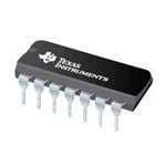
- 型号: LM2900N
- 制造商: Texas Instruments
- 库位|库存: xxxx|xxxx
- 要求:
| 数量阶梯 | 香港交货 | 国内含税 |
| +xxxx | $xxxx | ¥xxxx |
查看当月历史价格
查看今年历史价格
LM2900N产品简介:
ICGOO电子元器件商城为您提供LM2900N由Texas Instruments设计生产,在icgoo商城现货销售,并且可以通过原厂、代理商等渠道进行代购。 LM2900N价格参考¥0.98-¥2.81。Texas InstrumentsLM2900N封装/规格:线性 - 放大器 - 仪表,运算放大器,缓冲器放大器, 通用 放大器 4 电路 14-PDIP。您可以下载LM2900N参考资料、Datasheet数据手册功能说明书,资料中有LM2900N 详细功能的应用电路图电压和使用方法及教程。
Texas Instruments(德州仪器)的LM2900N是一款四通道低功耗运算放大器,适用于多种应用场景。其主要特点包括低静态电流、宽电源电压范围和高输入阻抗,使其在电池供电设备、传感器接口和工业控制等领域表现出色。

 1. 电池供电设备
LM2900N的低功耗特性非常适合用于便携式电子设备,如手持式测量仪器、无线传感器节点等。它能够在较低的工作电压下保持稳定的性能,延长电池寿命,同时提供足够的增益和带宽来处理信号。

 2. 传感器接口
该器件常用于各种传感器信号调理电路中,例如温度传感器、压力传感器和加速度计等。由于其高输入阻抗和低偏置电流,LM2900N能够准确地放大微弱的传感器信号,而不会对传感器负载产生影响。此外,其宽电源电压范围使得它可以适应不同的传感器供电需求。

 3. 工业控制系统
在工业自动化领域,LM2900N可用于构建精密的模拟信号处理电路,如PID控制器、滤波器和隔离放大器等。其四通道设计允许在一个封装内实现多个信号的独立处理,简化了电路板布局并提高了系统的集成度。

 4. 音频应用
尽管不是专门设计用于音频处理,但LM2900N也可以应用于一些低功耗音频设备中,如麦克风前置放大器或简单的音频混音器。其低噪声特性和合理的频率响应可以满足基本的音频信号放大需求。

 5. 测试与测量
在测试仪器中,LM2900N可以用作缓冲器或差分放大器,帮助提高信号完整性,减少噪声干扰。其稳定的工作特性和宽温度范围确保了在不同环境下的可靠性能。

总的来说,LM2900N凭借其低功耗、高性能和多通道设计,在众多需要精确信号处理的应用场景中发挥着重要作用。
| 参数 | 数值 |
| -3db带宽 | - |
| 产品目录 | 集成电路 (IC)半导体 |
| 描述 | IC OPAMP GP 2.5MHZ 14DIP运算放大器 - 运放 Quad |
| 产品分类 | Linear - Amplifiers - Instrumentation, OP Amps, Buffer Amps集成电路 - IC |
| 品牌 | Texas Instruments |
| 产品手册 | http://www.ti.com/litv/slos059 |
| 产品图片 |
|
| rohs | 符合RoHS无铅 / 符合限制有害物质指令(RoHS)规范要求 |
| 产品系列 | 放大器 IC,运算放大器 - 运放,Texas Instruments LM2900N- |
| 数据手册 | |
| 产品型号 | LM2900N |
| 产品目录页面 | |
| 产品种类 | 运算放大器 - 运放 |
| 供应商器件封装 | 14-PDIP |
| 关闭 | No Shutdown |
| 其它名称 | 296-9526-5 |
| 包装 | 管件 |
| 单位重量 | 1 g |
| 压摆率 | 20 V/µs |
| 双重电源电压 | +/- 3 V, +/- 5 V, +/- 9 V |
| 商标 | Texas Instruments |
| 增益带宽生成 | 2.5 MHz |
| 增益带宽积 | 2.5MHz |
| 安装类型 | 通孔 |
| 安装风格 | Through Hole |
| 封装 | Tube |
| 封装/外壳 | 14-DIP(0.300",7.62mm) |
| 封装/箱体 | PDIP-14 |
| 工作温度 | -40°C ~ 85°C |
| 工作电源电压 | 4.5 V to 32 V, +/- 2.2 V to +/- 16 V |
| 工厂包装数量 | 25 |
| 技术 | Bipolar |
| 放大器类型 | 通用 |
| 最大双重电源电压 | +/- 16 V |
| 最大工作温度 | + 85 C |
| 最小双重电源电压 | +/- 2.2 V |
| 最小工作温度 | - 40 C |
| 标准包装 | 25 |
| 电压-电源,单/双 (±) | 4.5 V ~ 32 V, ±2.2 V ~ 16 V |
| 电压-输入失调 | - |
| 电流-电源 | 6.2mA |
| 电流-输入偏置 | 30nA |
| 电流-输出/通道 | 18mA |
| 电源电流 | 10 mA |
| 电路数 | 4 |
| 系列 | LM2900 |
| 转换速度 | 20 V/us |
| 输入偏压电流—最大 | 200 nA |
| 输出电流 | 18 mA |
| 输出类型 | - |
| 通道数量 | 4 Channel |


- 商务部:美国ITC正式对集成电路等产品启动337调查
- 曝三星4nm工艺存在良率问题 高通将骁龙8 Gen1或转产台积电
- 太阳诱电将投资9.5亿元在常州建新厂生产MLCC 预计2023年完工
- 英特尔发布欧洲新工厂建设计划 深化IDM 2.0 战略
- 台积电先进制程称霸业界 有大客户加持明年业绩稳了
- 达到5530亿美元!SIA预计今年全球半导体销售额将创下新高
- 英特尔拟将自动驾驶子公司Mobileye上市 估值或超500亿美元
- 三星加码芯片和SET,合并消费电子和移动部门,撤换高东真等 CEO
- 三星电子宣布重大人事变动 还合并消费电子和移动部门
- 海关总署:前11个月进口集成电路产品价值2.52万亿元 增长14.8%


PDF Datasheet 数据手册内容提取
LM2900, LM3900 QUADRUPLE NORTON OPERATIONAL AMPLIFIERS SLOS059 – JULY 1979 – REVISED SEPTEMBER 1990 (cid:1) Wide Range of Supply Voltages, Single or N PACKAGE Dual Supplies (TOP VIEW) (cid:1) Wide Bandwidth (cid:1) 1IN+ 1 14 VCC Large Output Voltage Swing 2IN+ 2 13 3IN+ (cid:1) Output Short-Circuit Protection 2IN– 3 12 4IN+ (cid:1) Internal Frequency Compensation 2OUT 4 11 4IN– (cid:1) Low Input Bias Current 1OUT 5 10 4OUT (cid:1) 1IN– 6 9 3OUT Designed to Be Interchangeable With GND 7 8 3IN– National Semiconductor LM2900 and LM3900, Respectively description These devices consist of four independent, high- symbol (each amplifier) gain frequency-compensated Norton operational amplifiers that were designed specifically to operate from a single supply over a wide range of voltages. Operation from split supplies is also IN+ + possible. The low supply current drain is OUT essentially independent of the magnitude of the IN– – supply voltage. These devices provide wide band- width and large output voltage swing. The LM2900 is characterized for operation from –40°C to 85°C, and the LM3900 is characterized for operation from 0°C to 70°C. schematic (each amplifier) VCC Constant Current 200 m A Generator OUT IN– IN+ 1.3 mA PRODUCTION DATA information is current as of publication date. Copyright 1990, Texas Instruments Incorporated Products conform to specifications per the terms of Texas Instruments standard warranty. Production processing does not necessarily include testing of all parameters. POST OFFICE BOX 655303 • DALLAS, TEXAS 75265 1
LM2900, LM3900 QUADRUPLE NORTON OPERATIONAL AMPLIFIERS SLOS059 – JULY 1979 – REVISED SEPTEMBER 1990 absolute maximum ratings over operating free-air temperature range (unless otherwise noted) LM2900 LM3900 UNIT Supply voltage, VCC (see Note 1) 36 36 V Input current 20 20 mA Duration of output short circuit (one amplifier) to ground at (or below) 25°C free-air temperature unlimited unlimited (see Note 2) Continuous total dissipation See Dissipation Rating Table Operating free-air temperature range –40 to 85 0 to 70 °C Storage temperature range –65 to 150 –65 to 150 °C Lead temperature 1,6 mm (1/16 inch) from case for 10 seconds 260 260 °C NOTES: 1. All voltage values, except differential voltages, are with respect to the network ground terminal. 2. Short circuits from outputs to VCC can cause excessive heating and eventual destruction. DISSIPATION RATING TABLE TA ≤ 25°C DERATING FACTOR TA = 70°C TA = 85°C PACKAGE POWER RATING ABOVE TA = 25°C POWER RATING POWER RATING ° N 1150 mW 9.2 mW/ C 736 mW 598 mW recommended operating conditions LM2900 LM3900 UUNNIITT MIN MAX MIN MAX Supply voltage, VCC (single supply) 4.5 32 4.5 32 V Supply voltage, VCC+ (dual supply) 2.2 16 2.2 16 V Supply voltage, VCC– (dual supply) –2.2 –16 –2.2 –16 V Input current (see Note 3) –1 –1 mA Operating free-air temperature, TA –40 85 0 70 °C NOTE 3: Clamp transistors are included that prevent the input voltages from swinging below ground more than approximately –0.3 V. The negative input currents that may result from large signal overdrive with capacitive input coupling must be limited externally to values of approximately –1 mA. Negative input currents in excess of –4 mA causes the output voltage to drop to a low voltage. These values apply for any one of the input terminals. If more than one of the input terminals are simultaneously driven negative, maximum currents are reduced. Common-mode current biasing can be used to prevent negative input voltages. 2 POST OFFICE BOX 655303 • DALLAS, TEXAS 75265
LM2900, LM3900 QUADRUPLE NORTON OPERATIONAL AMPLIFIERS SLOS059 – JULY 1979 – REVISED SEPTEMBER 1990 electrical characteristics, V = 15 V, T = 25°C (unless otherwise noted) CC A LM2900 LM3900 PPAARRAAMMEETTEERR TTEESSTT CCOONNDDIITTIIOONNSS†† UUNNIITT MIN TYP MAX MIN TYP MAX TA = 25°C 30 200 30 200 IIIIBB IInnppuutt bbiiaass ccuurrrreenntt ((iinnvveerrttiinngg iinnppuutt)) IIII+ == 00 nnAA TA = Full range 300 300 MMiirrrroorr ggaaiinn IIII++ == 2200 mm AA ttoo 220000 mm AA 00.99 11.11 00.99 11.11 mm AA//mm AA TTAA == FFuullll rraannggee, Change in mirror gain See Note 4 2% 5% 2% 5% MMiirrrroorr ccuurrrreenntt VII++ = VII–,, TAA = Full rangge,, 1100 550000 1100 550000 mm AA See Note 4 Large-signal differential VO = 10 V, RL = 10 kW , AVD voltage amplification f = 100 Hz 1.2 2.8 1.2 2.8 V/mV ri Input resistance (inverting input) 1 1 MW ro Output resistance 8 8 kW Unity-gain bandwidth (inverting B1 input) 2.5 2.5 MHz Supply voltage rejection ratio kSVR (D VCC/D VIO) 70 70 dB RL = 2 kW 13.5 13.5 IIII+ == 00, VOH High-level output voltage II– = 0 VCC = 30 V, 29.5 29.5 V No load II+ = 0, II– = 10 m A, VOL Low-level output voltage RL = 2 kW 0.09 0.2 0.09 0.2 V Short-circuit output current II+ = 0, II– = 0, IOS (output internally high) VO = 0 –6 –18 –6 –10 mA Pulldown current 0.5 1.3 0.5 1.3 mA IOL Low-level output current‡ II– = 5 m A VOL = 1 V 5 5 mA ICC Supply current (four amplifiers) No load 6.2 10 6.2 10 mA †All characteristics are measured under open-loop conditions with zero common-mode voltage unless otherwise specified. Full range for TA is –40°C to 85°C for LM2900 and 0°C to 70°C for LM3900. ‡The output current-sink capability can be increased for large-signal conditions by overdriving the inverting input. NOTE 4: These parameters are measured with the output balanced midway between VCC and GND. operating characteristics, VCC± = ±15 V, TA = 25°C PARAMETER TEST CONDITIONS MIN TYP MAX UNIT Low-to-high output 0.5 SSRR SSlleeww rraattee aatt uunniittyy ggaaiinn VVOO == 1100 VV, CCLL == 110000 ppFF, RRLL == 22 kkWW VV//mm ss High-to-low output 20 POST OFFICE BOX 655303 • DALLAS, TEXAS 75265 3
LM2900, LM3900 QUADRUPLE NORTON OPERATIONAL AMPLIFIERS SLOS059 – JULY 1979 – REVISED SEPTEMBER 1990 TYPICAL CHARACTERISTICS† INPUT BIAS CURRENT (INVERTING INPUT) MIRROR GAIN vs vs FREE-AIR TEMPERATURE FREE-AIR TEMPERATURE 80 1.2 VCC = 15 V VCC = 15 V 70 VO = 7.5 V 1.15 II+ = 10 m A II+ = 0 A 60 1.1 n as Current – 4500 – Mirror Gain 1.015 Bi + – Input 30 /III – 0.95 B 20 0.9 II 10 0.85 0 0.8 –75 –50 –25 0 25 50 75 100 –75 –50 –25 0 25 50 75 100 125 ° TA – Free-Air Temperature – °C TA – Free-Air Temperature – C Figure 1 Figure 2 LARGE SIGNAL LARGE SIGNAL DIFFERENTIAL VOLTAGE AMPLIFICATION DIFFERENTIAL VOLTAGE AMPLIFICATION vs vs FREQUENCY SUPPLY VOLTAGE 104 104 RL≥10 kW VCC = 1°5 V TA = 25 C n n o o cati 103 cati 103 mplifi RL = 2 kW mplifi A A e e g g olta 102 olta 102 V V al al nti nti e e er er Diff 10 Diff 10 – D – D RL = 10 kW AV AV TA = 25°C 1 1 100 1 k 10 k 100 k 1 M 10 M 0 5 10 15 20 25 30 f – Frequency – Hz VCC – Supply Voltage – V Figure 3 Figure 4 †Data at high and low temperatures are applicable only within the rated operating free-air temperature ranges of the various devices. 4 POST OFFICE BOX 655303 • DALLAS, TEXAS 75265
LM2900, LM3900 QUADRUPLE NORTON OPERATIONAL AMPLIFIERS SLOS059 – JULY 1979 – REVISED SEPTEMBER 1990 TYPICAL CHARACTERISTICS† LARGE SIGNAL DIFFERENTIAL VOLTAGE AMPLIFICATION SUPPLY VOLTAGE REJECTION RATIO vs vs FREE-AIR TEMPERATURE FREQUENCY 104 100 dB 90 VCC = 15 V n – TA = 25°C o o cati 103 Rati 80 plifi on 70 e Am ejecti 60 g R olta 102 ge 50 V a erential pply Volt 3400 Diff 10 Su – – 20 D VCC = 15 V R AV VROL == 1100 kVW KSV 10 1 0 –75 –50 –25 0 25 50 75 100 125 100 400 1 k 4k 10 k 40 k 100 k 400 k 1 M TA – Free-Air Temperature – °C f – Frequency – Hz Figure 5 Figure 6 SHORT-CIRCUIT OUTPUT CURRENT PEAK-TO-PEAK OUTPUT VOLTAGE (OUTPUT INTERNALLY HIGH) vs vs FREQUENCY SUPPLY VOLTAGE 16 30 e – V 14 RVCL C= =2 1k5W V mA 25 VIIO+ == 00 ut Voltag 12 ITIA+ == 205°C urrent – 20 II– = 0 TA = 0°C utp 10 ut C k O utp TA = 25°C k-To-Pea 68 Circuit O 15 Pea ort- 10 Á– Á4 Sh ÁP)Á – O(P 2 OS 5 ÁVÁ I 0 0 1 k 10 k 100 k 1 M 10 M 0 5 10 15 20 25 30 f – Frequency – Hz VCC – Supply Voltage – V Figure 7 Figure 8 †Data at high and low temperatures are applicable only within the rated operating free-air temperature ranges of the various devices. POST OFFICE BOX 655303 • DALLAS, TEXAS 75265 5
LM2900, LM3900 QUADRUPLE NORTON OPERATIONAL AMPLIFIERS SLOS059 – JULY 1979 – REVISED SEPTEMBER 1990 TYPICAL CHARACTERISTICS† LOW-LEVEL OUTPUT CURRENT PULLDOWN CURRENT vs vs SUPPLY VOLTAGE SUPPLY VOLTAGE 60 2 VOL = 1 V 1.8 – mA 50 ITIA+ == 025°C 1.6 TA = –40°C nt Output Curre 3400 II– = 100 m A Current – mA 11..124 TA = 25°C evel own 0.8 TA = 85°C L d ow- 20 Pull 0.6 L – II– = 10 m A L 0.4 O I 10 II– = 5 m A 0.2 0 0 0 5 10 15 20 25 30 0 5 10 15 20 25 30 VCC – Supply Voltage – V VCC – Supply Voltage – V Figure 9 Figure 10 PULLDOWN CURRENT TOTAL SUPPLY CURRENT vs vs FREE-AIR TEMPERATURE SUPPLY VOLTAGE 2 8 VCC = 15 V 1.8 7 1.6 A 6 A m m 1.4 – nt – 1.2 rent 5 rre Cur Cu 1 y 4 wn 0.8 uppl o S 3 Pulld 0.6 otal – T 2 0.4 C TA = 25°C C I 1 No Signal 0.2 No Load 0 0 –75 –50 –25 0 25 50 75 100 125 0 5 10 15 20 25 30 TA – Free-Air Temperature –°C VCC – Supply Voltage – V Figure 11 Figure 12 †Data at high and low temperatures are applicable only within the rated operating free-air temperature ranges of the various devices. 6 POST OFFICE BOX 655303 • DALLAS, TEXAS 75265
LM2900, LM3900 QUADRUPLE NORTON OPERATIONAL AMPLIFIERS SLOS059 – JULY 1979 – REVISED SEPTEMBER 1990 APPLICATION INFORMATION Norton (or current-differencing) amplifiers can be used in most standard general-purpose operational amplifier applications. Performance as a dc amplifier in a single-power-supply mode is not as precise as a standard integrated-circuit operational amplifier operating from dual supplies. Operation of the amplifier can best be understood by noting that input currents are differenced at the inverting input terminal and this current then flows through the external feedback resistor to produce the output voltage. Common-mode current biasing is generally useful to allow operating with signal levels near (or even below) ground. Internal transistors clamp negative input voltages at approximately –0.3 V but the magnitude of current flow has to be limited by the external input network. For operation at high temperature, this limit should be approximately –100 m A. Noise immunity of a Norton amplifier is less than that of standard bipolar amplifiers. Circuit layout is more critical since coupling from the output to the noninverting input can cause oscillations. Care must also be exercised when driving either input from a low-impedance source. A limiting resistor should be placed in series with the input lead to limit the peak input current. Current up to 20 mA will not damage the device, but the current mirror on the noninverting input will saturate and cause a loss of mirror gain at higher current levels, especially at high operating temperatures. V+ 1 MW 1 MW 10 kW 1 kW 1 MW Input – 30 kW 100 kW + Output 91 kW ≈ IO 1 mA per input volt Figure 13. Voltage-Controlled Current Source V+ 1 MW 1 MW – Output 100 kW Input + 100 kW 1 kW ≈ IO 1 mA per input volt Figure 14. Voltage-Controlled Current Sink POST OFFICE BOX 655303 • DALLAS, TEXAS 75265 7
PACKAGE OPTION ADDENDUM www.ti.com 6-Feb-2020 PACKAGING INFORMATION Orderable Device Status Package Type Package Pins Package Eco Plan Lead/Ball Finish MSL Peak Temp Op Temp (°C) Device Marking Samples (1) Drawing Qty (2) (6) (3) (4/5) LM2900D ACTIVE SOIC D 14 50 Green (RoHS NIPDAU Level-1-260C-UNLIM -40 to 85 LM2900 & no Sb/Br) LM2900DR ACTIVE SOIC D 14 2500 Green (RoHS NIPDAU Level-1-260C-UNLIM -40 to 85 LM2900 & no Sb/Br) LM2900DR ACTIVE SOIC D 14 2500 Green (RoHS NIPDAU Level-1-260C-UNLIM -40 to 85 LM2900 & no Sb/Br) LM2900DR ACTIVE SOIC D 14 2500 Green (RoHS NIPDAU Level-1-260C-UNLIM -40 to 85 LM2900 & no Sb/Br) LM2900N ACTIVE PDIP N 14 25 Green (RoHS NIPDAU N / A for Pkg Type -40 to 85 LM2900N & no Sb/Br) LM2900N ACTIVE PDIP N 14 25 Green (RoHS NIPDAU N / A for Pkg Type -40 to 85 LM2900N & no Sb/Br) LM2900N ACTIVE PDIP N 14 25 Green (RoHS NIPDAU N / A for Pkg Type -40 to 85 LM2900N & no Sb/Br) LM2900NE4 ACTIVE PDIP N 14 25 Green (RoHS NIPDAU N / A for Pkg Type -40 to 85 LM2900N & no Sb/Br) LM2900NE4 ACTIVE PDIP N 14 25 Green (RoHS NIPDAU N / A for Pkg Type -40 to 85 LM2900N & no Sb/Br) LM2900NE4 ACTIVE PDIP N 14 25 Green (RoHS NIPDAU N / A for Pkg Type -40 to 85 LM2900N & no Sb/Br) LM3900D ACTIVE SOIC D 14 50 Green (RoHS NIPDAU Level-1-260C-UNLIM 0 to 70 LM3900 & no Sb/Br) LM3900D ACTIVE SOIC D 14 50 Green (RoHS NIPDAU Level-1-260C-UNLIM 0 to 70 LM3900 & no Sb/Br) LM3900D ACTIVE SOIC D 14 50 Green (RoHS NIPDAU Level-1-260C-UNLIM 0 to 70 LM3900 & no Sb/Br) LM3900DR ACTIVE SOIC D 14 2500 Green (RoHS NIPDAU Level-1-260C-UNLIM 0 to 70 LM3900 & no Sb/Br) LM3900DR ACTIVE SOIC D 14 2500 Green (RoHS NIPDAU Level-1-260C-UNLIM 0 to 70 LM3900 & no Sb/Br) LM3900DR ACTIVE SOIC D 14 2500 Green (RoHS NIPDAU Level-1-260C-UNLIM 0 to 70 LM3900 & no Sb/Br) LM3900N ACTIVE PDIP N 14 25 Green (RoHS NIPDAU N / A for Pkg Type 0 to 70 LM3900N & no Sb/Br) Addendum-Page 1
PACKAGE OPTION ADDENDUM www.ti.com 6-Feb-2020 Orderable Device Status Package Type Package Pins Package Eco Plan Lead/Ball Finish MSL Peak Temp Op Temp (°C) Device Marking Samples (1) Drawing Qty (2) (6) (3) (4/5) LM3900N ACTIVE PDIP N 14 25 Green (RoHS NIPDAU N / A for Pkg Type 0 to 70 LM3900N & no Sb/Br) LM3900N ACTIVE PDIP N 14 25 Green (RoHS NIPDAU N / A for Pkg Type 0 to 70 LM3900N & no Sb/Br) LM3900NE4 ACTIVE PDIP N 14 25 Green (RoHS NIPDAU N / A for Pkg Type 0 to 70 LM3900N & no Sb/Br) LM3900NE4 ACTIVE PDIP N 14 25 Green (RoHS NIPDAU N / A for Pkg Type 0 to 70 LM3900N & no Sb/Br) LM3900NE4 ACTIVE PDIP N 14 25 Green (RoHS NIPDAU N / A for Pkg Type 0 to 70 LM3900N & no Sb/Br) (1) The marketing status values are defined as follows: ACTIVE: Product device recommended for new designs. LIFEBUY: TI has announced that the device will be discontinued, and a lifetime-buy period is in effect. NRND: Not recommended for new designs. Device is in production to support existing customers, but TI does not recommend using this part in a new design. PREVIEW: Device has been announced but is not in production. Samples may or may not be available. OBSOLETE: TI has discontinued the production of the device. (2) RoHS: TI defines "RoHS" to mean semiconductor products that are compliant with the current EU RoHS requirements for all 10 RoHS substances, including the requirement that RoHS substance do not exceed 0.1% by weight in homogeneous materials. Where designed to be soldered at high temperatures, "RoHS" products are suitable for use in specified lead-free processes. TI may reference these types of products as "Pb-Free". RoHS Exempt: TI defines "RoHS Exempt" to mean products that contain lead but are compliant with EU RoHS pursuant to a specific EU RoHS exemption. Green: TI defines "Green" to mean the content of Chlorine (Cl) and Bromine (Br) based flame retardants meet JS709B low halogen requirements of <=1000ppm threshold. Antimony trioxide based flame retardants must also meet the <=1000ppm threshold requirement. (3) MSL, Peak Temp. - The Moisture Sensitivity Level rating according to the JEDEC industry standard classifications, and peak solder temperature. (4) There may be additional marking, which relates to the logo, the lot trace code information, or the environmental category on the device. (5) Multiple Device Markings will be inside parentheses. Only one Device Marking contained in parentheses and separated by a "~" will appear on a device. If a line is indented then it is a continuation of the previous line and the two combined represent the entire Device Marking for that device. (6) Lead/Ball Finish - Orderable Devices may have multiple material finish options. Finish options are separated by a vertical ruled line. Lead/Ball Finish values may wrap to two lines if the finish value exceeds the maximum column width. Important Information and Disclaimer:The information provided on this page represents TI's knowledge and belief as of the date that it is provided. TI bases its knowledge and belief on information provided by third parties, and makes no representation or warranty as to the accuracy of such information. Efforts are underway to better integrate information from third parties. TI has taken and Addendum-Page 2
PACKAGE OPTION ADDENDUM www.ti.com 6-Feb-2020 continues to take reasonable steps to provide representative and accurate information but may not have conducted destructive testing or chemical analysis on incoming materials and chemicals. TI and TI suppliers consider certain information to be proprietary, and thus CAS numbers and other limited information may not be available for release. In no event shall TI's liability arising out of such information exceed the total purchase price of the TI part(s) at issue in this document sold by TI to Customer on an annual basis. Addendum-Page 3
PACKAGE MATERIALS INFORMATION www.ti.com 14-Jul-2012 TAPE AND REEL INFORMATION *Alldimensionsarenominal Device Package Package Pins SPQ Reel Reel A0 B0 K0 P1 W Pin1 Type Drawing Diameter Width (mm) (mm) (mm) (mm) (mm) Quadrant (mm) W1(mm) LM2900DR SOIC D 14 2500 330.0 16.4 6.5 9.0 2.1 8.0 16.0 Q1 LM3900DR SOIC D 14 2500 330.0 16.4 6.5 9.0 2.1 8.0 16.0 Q1 PackMaterials-Page1
PACKAGE MATERIALS INFORMATION www.ti.com 14-Jul-2012 *Alldimensionsarenominal Device PackageType PackageDrawing Pins SPQ Length(mm) Width(mm) Height(mm) LM2900DR SOIC D 14 2500 367.0 367.0 38.0 LM3900DR SOIC D 14 2500 367.0 367.0 38.0 PackMaterials-Page2
None
None
None
IMPORTANTNOTICEANDDISCLAIMER TI PROVIDES TECHNICAL AND RELIABILITY DATA (INCLUDING DATASHEETS), DESIGN RESOURCES (INCLUDING REFERENCE DESIGNS), APPLICATION OR OTHER DESIGN ADVICE, WEB TOOLS, SAFETY INFORMATION, AND OTHER RESOURCES “AS IS” AND WITH ALL FAULTS, AND DISCLAIMS ALL WARRANTIES, EXPRESS AND IMPLIED, INCLUDING WITHOUT LIMITATION ANY IMPLIED WARRANTIES OF MERCHANTABILITY, FITNESS FOR A PARTICULAR PURPOSE OR NON-INFRINGEMENT OF THIRD PARTY INTELLECTUAL PROPERTY RIGHTS. These resources are intended for skilled developers designing with TI products. You are solely responsible for (1) selecting the appropriate TI products for your application, (2) designing, validating and testing your application, and (3) ensuring your application meets applicable standards, and any other safety, security, or other requirements. These resources are subject to change without notice. TI grants you permission to use these resources only for development of an application that uses the TI products described in the resource. Other reproduction and display of these resources is prohibited. No license is granted to any other TI intellectual property right or to any third party intellectual property right. TI disclaims responsibility for, and you will fully indemnify TI and its representatives against, any claims, damages, costs, losses, and liabilities arising out of your use of these resources. TI’s products are provided subject to TI’s Terms of Sale (www.ti.com/legal/termsofsale.html) or other applicable terms available either on ti.com or provided in conjunction with such TI products. TI’s provision of these resources does not expand or otherwise alter TI’s applicable warranties or warranty disclaimers for TI products. Mailing Address: Texas Instruments, Post Office Box 655303, Dallas, Texas 75265 Copyright © 2020, Texas Instruments Incorporated