ICGOO在线商城 > 集成电路(IC) > 线性 - 放大器 - 仪表,运算放大器,缓冲器放大器 > AD8366ACPZ-R7
 Datasheet下载
- 型号: AD8366ACPZ-R7
- 制造商: Analog
- 库位|库存: xxxx|xxxx
- 要求:
| 数量阶梯 | 香港交货 | 国内含税 |
| +xxxx | $xxxx | ¥xxxx |
查看当月历史价格
查看今年历史价格
AD8366ACPZ-R7产品简介:
ICGOO电子元器件商城为您提供AD8366ACPZ-R7由Analog设计生产,在icgoo商城现货销售,并且可以通过原厂、代理商等渠道进行代购。 AD8366ACPZ-R7价格参考¥71.61-¥106.29。AnalogAD8366ACPZ-R7封装/规格:线性 - 放大器 - 仪表,运算放大器,缓冲器放大器, 可变增益 放大器 2 电路 差分 32-LFCSP-VQ(5x5)。您可以下载AD8366ACPZ-R7参考资料、Datasheet数据手册功能说明书,资料中有AD8366ACPZ-R7 详细功能的应用电路图电压和使用方法及教程。
AD8366ACPZ-R7 是 Analog Devices Inc. 生产的一款线性放大器,属于仪表、运算放大器和缓冲器放大器类别。该型号具有低功耗、高精度和宽频率响应的特点,适用于多种场景。以下是其主要应用场景:

 1. 通信系统
AD8366ACPZ-R7 可用于无线通信系统中的信号调理和增益控制。例如,在射频(RF)接收机中,它可以用作可变增益放大器(VGA),调整信号强度以适应后续处理阶段的需求。

 2. 医疗设备
在医疗电子领域,这款放大器可用于心电图(ECG)、脑电图(EEG)等生物信号的放大和处理。其低噪声特性有助于提高信号质量,确保测量结果的准确性。

 3. 工业自动化
AD8366ACPZ-R7 在工业自动化中可用于传感器信号的放大和处理。例如,压力传感器、温度传感器或位移传感器输出的微弱信号可以通过该放大器进行增强,以便于进一步的数据采集和分析。

 4. 音频处理
由于其高线性和低失真特性,AD8366ACPZ-R7 可应用于音频设备中,如麦克风前置放大器或音频信号处理器,提供高质量的声音放大。

 5. 测试与测量
在测试仪器中,如示波器、信号发生器等,该放大器可用于信号的精确放大和调节,满足高精度测试需求。

 6. 消费电子产品
AD8366ACPZ-R7 还可以用于消费电子产品中的信号处理模块,如智能家居设备、便携式音频设备等,提供稳定的信号放大功能。

 特点总结
- 低功耗:适合电池供电设备。
- 高线性度:保证信号不失真。
- 宽频率范围:支持从低频到高频的应用。
- 小封装:便于集成到紧凑型设计中。

这些特点使 AD8366ACPZ-R7 成为多种应用的理想选择,尤其是在需要高性能信号处理的场合。
| 参数 | 数值 |
| -3db带宽 | 600MHz |
| 产品目录 | 集成电路 (IC) |
| 描述 | IC OPAMP VGA 600MHZ 32LFCSP |
| 产品分类 | Linear - Amplifiers - Instrumentation, OP Amps, Buffer Amps |
| 品牌 | Analog Devices Inc |
| 数据手册 | |
| 产品图片 |
|
| 产品型号 | AD8366ACPZ-R7 |
| PCN组件/产地 | |
| rohs | 无铅 / 符合限制有害物质指令(RoHS)规范要求 |
| 产品系列 | - |
| 产品培训模块 | http://www.digikey.cn/PTM/IndividualPTM.page?site=cn&lang=zhs&ptm=30008http://www.digikey.cn/PTM/IndividualPTM.page?site=cn&lang=zhs&ptm=26202 |
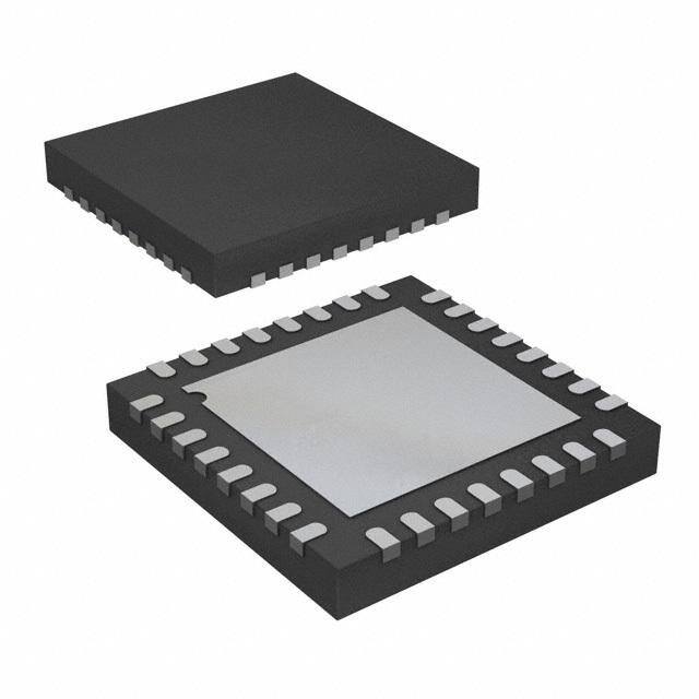
| 供应商器件封装 | 32-LFCSP-VQ(5x5) |
| 其它名称 | AD8366ACPZ-R7TR |
| 包装 | 带卷 (TR) |
| 压摆率 | 1100 V/µs |
| 增益带宽积 | - |
| 安装类型 | 表面贴装 |
| 封装/外壳 | 32-VFQFN 裸露焊盘,CSP |
| 工作温度 | -40°C ~ 85°C |
| 放大器类型 | 可变增益 |
| 标准包装 | 1,500 |
| 电压-电源,单/双 (±) | 4.75 V ~ 5.25 V |
| 电压-输入失调 | - |
| 电流-电源 | 180mA |
| 电流-输入偏置 | - |
| 电流-输出/通道 | - |
| 电路数 | 2 |
| 视频文件 | http://www.digikey.cn/classic/video.aspx?PlayerID=1364138032001&width=640&height=505&videoID=2245193153001http://www.digikey.cn/classic/video.aspx?PlayerID=1364138032001&width=640&height=505&videoID=2245193159001 |
| 输出类型 | 差分 |


- 商务部:美国ITC正式对集成电路等产品启动337调查
- 曝三星4nm工艺存在良率问题 高通将骁龙8 Gen1或转产台积电
- 太阳诱电将投资9.5亿元在常州建新厂生产MLCC 预计2023年完工
- 英特尔发布欧洲新工厂建设计划 深化IDM 2.0 战略
- 台积电先进制程称霸业界 有大客户加持明年业绩稳了
- 达到5530亿美元!SIA预计今年全球半导体销售额将创下新高
- 英特尔拟将自动驾驶子公司Mobileye上市 估值或超500亿美元
- 三星加码芯片和SET,合并消费电子和移动部门,撤换高东真等 CEO
- 三星电子宣布重大人事变动 还合并消费电子和移动部门
- 海关总署:前11个月进口集成电路产品价值2.52万亿元 增长14.8%


PDF Datasheet 数据手册内容提取
DC to 600 MHz, Dual-Digital Variable Gain Amplifiers Data Sheet AD8366 FEATURES FUNCTIONAL BLOCK DIAGRAM Matched pair of differential, digitally controlled VGAs CA SA MA MA SOA PA MA NB Gain range: 4.5 dB to 20.25 dB DE OF CC VC VP OP OP SE 0.25 dB gain step size Operating frequency DC to 150 MHz (2 V p-p) VPSIA BIT0/CS 3 dB bandwidth: 600 MHz IPPA BIT1/SDAT Noise figure (NF) IPMA BIT2/SCLK 11.4 dB at 10 MHz at maximum gain 18 dB at 10 MHz at minimum gain ENBL BIT3 DIGITAL GAIN OIP3: 45 dBm at 10 MHz ICOM CONTROL LOGIC OCOM HD2/HD3 IPMB BIT4 Better than −90 dBc for 2 V p-p output at 10 MHz at IPPB BIT 5 maximum gain Differential input and output VPSIB DENA Adjustable output common-mode Optional dc output offset correction SPeorwiaelr/-pdaorwalnle fle matoudree gain control DECB OFSB CCMB VCMB VPSOB OPPB OPMB DENB 07584-001 Figure 1. Single 5 V supply operation APPLICATIONS Baseband I/Q receivers Diversity receivers Wideband ADC drivers GENERAL DESCRIPTION The AD8366 is a matched pair of fully differential, low noise and The output common-mode voltage defaults to V /2 but can POS low distortion, digitally programmable variable gain amplifiers be programmed via the VCMA and VCMB pins over a range (VGAs). The gain of each amplifier can be programmed separately of voltages. The input common-mode voltage also defaults or simultaneously over a range of 4.5 dB to 20.25 dB in steps of to V /2 but can be driven down to 1.5 V. A built-in, dc offset POS 0.25 dB. The amplifier offers flat frequency performance from dc compensation loop can be used to eliminate dc offsets from prior to 70 MHz, independent of gain code. stages in the signal chain. This loop can also be disabled if dc- coupled operation is desired. The AD8366 offers excellent spurious-free dynamic range, suitable for driving high resolution analog-to-digital converters (ADCs). The digital interface allows for parallel or serial mode gain The NF at maximum gain is 11.4 dB at 10 MHz and increases programming. The AD8366 operates from a 4.75 V to 5.25 V ~2 dB for every 4 dB decrease in gain. Over the entire gain range, supply and consumes typically 180 mA. When disabled, the the HD3/HD2 are better than −90 dBc for 2 V p-p at the output at part consumes roughly 3 mA. The AD8366 is fabricated using 10 MHz into 200 Ω. The two-tone intermodulation distortion of Analog Devices, Inc., advanced silicon-germanium bipolar −90 dBc into 200 Ω translates to an OIP3 of 45 dBm (38 dBVrms). process, and it is available in a 32-lead exposed paddle LFCSP The differential input impedance of 200 Ω provides a well-defined package. Performance is specified over the −40°C to +85°C termination. The differential output has a low impedance of ~25 Ω. temperature range. Rev. B Document Feedback Information furnished by Analog Devices is believed to be accurate and reliable. However, no responsibility is assumed by Analog Devices for its use, nor for any infringements of patents or other One Technology Way, P.O. Box 9106, Norwood, MA 02062-9106, U.S.A. rights of third parties that may result from its use. Specifications subject to change without notice. No license is granted by implication or otherwise under any patent or patent rights of Analog Devices. Tel: 781.329.4700 ©2010–2017 Analog Devices, Inc. All rights reserved. Trademarks and registered trademarks are the property of their respective owners. Technical Support www.analog.com
AD8366 Data Sheet TABLE OF CONTENTS Features .............................................................................................. 1 Output Differential Offset Correction .................................... 15 Applications ....................................................................................... 1 Output Common-Mode Control ............................................. 15 Functional Block Diagram .............................................................. 1 Gain Control Interface ............................................................... 16 General Description ......................................................................... 1 Applications Information .............................................................. 17 Revision History ............................................................................... 2 Basic Connections ...................................................................... 17 Specifications ..................................................................................... 3 Direct Conversion Receiver Design ......................................... 18 Parallel and Serial Interface timing ............................................ 5 Quadrature Errors and Image Rejection ................................. 18 Absolute Maximum Ratings ............................................................ 6 Low Frequency IMD3 Performance ........................................ 19 ESD Caution .................................................................................. 6 Baseband Interface ..................................................................... 21 Pin Configuration and Function Descriptions ............................. 7 Characterization Setups ................................................................. 22 Typical Performance Characteristics ............................................. 8 Evaluation Board ............................................................................ 25 Circuit Description ......................................................................... 15 Outline Dimensions ....................................................................... 28 Inputs ........................................................................................... 15 Ordering Guide .......................................................................... 28 Outputs ........................................................................................ 15 REVISION HISTORY 8/2017—Rev. A to Rev. B Change to Figure 4 ........................................................................... 7 Updated Outline Dimensions ....................................................... 28 Changes to Ordering Guide .......................................................... 28 3/2011—Rev. 0 to Rev. A Changes to Table 2, Internal Power Dissipation Value ................ 6 10/2010—Revision 0: Initial Version Rev. B | Page 2 of 28
Data Sheet AD8366 SPECIFICATIONS V = 5 V, T = 25°C, Z = 200 Ω, Z = 200 Ω, f = 10 MHz, unless otherwise noted. S A S L Table 1. Parameter Test Conditions/Comments Min Typ Max Unit DYNAMIC PERFORMANCE Bandwidth 3 dB; all gain codes 600 MHz 1 dB; all gain codes 200 MHz Slew Rate Maximum gain 1100 V/µs Minimum gain 1500 V/µs INPUT STAGE IPPA, IPMA, IPPB, IPMB Linear Input Swing At minimum gain A = 4.5 dB, 1 dB gain compression 3.6 V p-p V Differential Input Impedance 217 Ω Minimum Input Common-Mode Voltage 1.5 V Maximum Input Common-Mode Voltage V /2 + 0.075 V POS Input pins left floating V /2 V POS GAIN Minimum Voltage Gain 4.5 dB Maximum Voltage Gain 20.25 dB Gain Step Size All gain codes 0.25 dB Gain Step Accuracy All gain codes ±0.25 dB Gain Flatness Maximum gain, DC to 70 MHz 0.1 dB Gain Mismatch Channel A/Channel B at minimum/maximum gain code 0.1 dB Group Delay Flatness All gain codes, 20% fractional bandwidth, f < 100 MHz <0.5 ns C Mismatch Channel A and Channel B at same gain code 2 ps Gain Step Response Maximum gain to minimum gain 30 ns Minimum gain to maximum gain 60 ns Common-Mode Rejection Ratio −66.2 dB OUTPUT STAGE OPPA, OPMA, OPPB, OPMB, VCMA, VCMB Linear Output Swing 1 dB gain compression 6 V p-p Differential Output Impedance 28 Ω Output DC Offset Inputs shorted, offset loop disabled at −10/−30 mV minimum/maximum gain Inputs shorted, offset loop enabled (across all gain codes) 10 mV Minimum Output Common-Mode Voltage HD3, HD2 > −90 dBc, 2 V p-p output 1.6 V Maximum Output Common-Mode Voltage HD3, HD2 > −90 dBc, 2 V p-p output 3 V VCMA and VCMB left floating V /2 V POS Common-Mode Setpoint Input Impedance 4 kΩ NOISE/DISTORTION 3 MHz Noise Figure Maximum gain 11.3 dB Minimum gain 18.2 dB Second Harmonic 2 V p-p output, maximum gain −82 dBc 2 V p-p output, minimum gain −82 dBc Third Harmonic 2 V p-p output, maximum gain −87 dBc 2 V p-p output, minimum gain −90 dBc OIP31 2 V p-p composite, maximum gain 34 dBVrms 2 V p-p composite, minimum gain 35 dBVrms OIP21 2 V p-p composite, maximum gain 76 dBVrms 2 V p-p composite, minimum gain 76 dBVrms Output 1 dB Compression Point1 Maximum gain 6.7 dBVrms Minimum gain 6.9 dBVrms Rev. B | Page 3 of 28
AD8366 Data Sheet Parameter Test Conditions/Comments Min Typ Max Unit 10 MHz Noise Figure Maximum gain 11.4 dB Minimum gain 18 dB Second Harmonic 2 V p-p output, maximum gain −97 dBc 2 V p-p output, minimum gain −96 dBc Third Harmonic 2 V p-p output, maximum gain −97 dBc 2 V p-p output, minimum gain −90 dBc OIP31 2 V p-p composite, maximum gain 38 dBVrms 2 V p-p composite, minimum gain 36 dBVrms OIP21 2 V p-p composite, maximum gain 72 dBVrms 2 V p-p composite, minimum gain 76 dBVrms Output 1 dB Compression Point1 Maximum gain 7 dBVrms Minimum gain 6.7 dBVrms 50 MHz Noise Figure Maximum gain 11.8 dB Minimum gain 18.2 dB Second Harmonic 2 V p-p output, maximum gain −82 dBc 2 V p-p output, minimum gain −84 dBc Third Harmonic 2 V p-p output, maximum gain −80 dBc 2 V p-p output, minimum gain −71 dBc OIP31 2 V p-p composite, maximum gain 32 dBVrms 2 V p-p composite, minimum gain 26 dBVrms OIP21 2 V p-p composite, maximum gain 71 dBVrms 2 V p-p composite, minimum gain 78 dBVrms Output 1 dB Compression Point1 Maximum gain 6.7 dBVrms Minimum gain 6.7 dBVrms DIGITAL LOGIC SENB, DENA, DENB, BIT0, BIT1, BIT2, BIT3, BIT4, BIT5 Input High Voltage, V 2.2 V INH Input Low Voltage, V 1.2 V INL Input Capacitance, C 1 pF IN Input Resistance, R 50 kΩ IN SPI INTERFACE TIMING SENB = high f Serial clock frequency (maximum) 44.4 MHz SCLK t CS rising edge to first SCLK rising edge (minimum) 7.5 ns 1 t SCLK high pulse width (minimum) 7.5 ns 2 t SCLK low pulse width (minimum) 15 ns 3 t SCLK falling edge to CS low (minimum) 7.5 ns 4 t SDAT setup time (minimum) 7.5 ns 5 t SDAT hold time (minimum) 15 ns 6 PARALLEL PORT TIMING SENB = low t DENA/DENB high pulse width (minimum) 7.5 ns 7 t DENA/DENB low pulse width (minimum) 15 ns 8 t BITx setup time (minimum) 7.5 ns 9 t BITx hold time (minimum) 7.5 ns 10 POWER AND ENABLE VPSIA, VPSIB, VPSOA, VPSOB, ICOM, OCOM, ENBL Supply Voltage Range 4.75 5.25 V Total Supply Current ENBL = 5 V 180 mA Disable Current ENBL = 0 V 3.2 mA Disable Threshold 1.65 V Enable Response Time Delay following high-to-low transition until device 150 ns meets full specifications Disable Response Time Delay following low-to-high transition until device 3 µs produces full attenuation 1 To convert to dBm for a 200 Ω load impedance, add 7 dB to the dBVrms value. Rev. B | Page 4 of 28
Data Sheet AD8366 PARALLEL AND SERIAL INTERFACE TIMING CS t t t1 t2 3 4 SCLK t t 5 6 SDAT X B-LSB B-MSB A-LSB A-MSB X SENB ALWAYS HIGH 07584-003 Figure 2. SPI Port Timing Diagram BIT[5:0] GAIN A GAIN B GAIN A, GAIN B DENA t9 t10 DENB t7 t8 SENB ALWAYS LOW 07584-004 Figure 3. Parallel Port Timing Diagram Rev. B | Page 5 of 28
AD8366 Data Sheet ABSOLUTE MAXIMUM RATINGS Stresses at or above those listed under Absolute Maximum Table 2. Ratings may cause permanent damage to the product. This is a Parameter Rating stress rating only; functional operation of the product at these Supply Voltages, VPSIx and VPSOx 5.5 V or any other conditions above those indicated in the operational ENBL, SENB, DENA, DENB, BIT0, BIT1, BIT2, 5.5 V BIT3, BIT4, BIT5 section of this specification is not implied. Operation beyond IPPA, IPMA, IPPB, IPMB 5.5 V the maximum operating conditions for extended periods may OPPA, OPMA, OPPB, OPMB 5.5 V affect product reliability. OFSA, OFSB 5.5 V DECA, DECB, VCMA, VCMB, CCMA, CCMB 5.5 V ESD CAUTION Internal Power Dissipation 1.4 W θ (With Pad Soldered to Board) 45.4°C/W JA Maximum Junction Temperature 150°C Operating Temperature Range −40°C to +85°C Storage Temperature Range −65°C to +150°C Lead Temperature (Soldering, 60 sec) 300°C Rev. B | Page 6 of 28
Data Sheet AD8366 PIN CONFIGURATION AND FUNCTION DESCRIPTIONS CASAMAMASOAPAMANB EFCCPPPE DOCVVOOS 21098765 33322222 VPSIA1 24BIT0/CS IPPA2 23BIT1/SDAT IPMA3 22BIT2/SCLK AD8366 ENBL 4 21BIT3 ICOM5 TOP VIEW 20OCOM (Not to Scale) IPMB6 19BIT4 IPPB7 18BIT5 VPSIB8 17DENA 90123456 1111111 BBBBBBBB CSMMOPMN DEOFCCVCPSOPOPDE V N1 . O TTTHOEE SG ERXOPUONSDE.D PAD MUST BE CONNECTED 07584-028 Figure 4. Pin Configuration Table 3. Pin Function Descriptions Pin No. Mnemonic Description 1, 8, 13, 28 VPSIA, VPSIB, VPSOB, Input and Output Stage Positive Supply Voltage (4.75 V to 5.25 V). VPSOA 2, 3, 6, 7 IPPA, IPMA, IPMB, Differential Inputs. IPPB 4 ENBL Chip Enable. Pull this pin high to enable. 5, 20 ICOM, OCOM Input and Output Ground Pins. Connect these pins via the lowest possible impedance to ground. 9, 32 DECB, DECA V /2 Reference Decoupling Node. Connect a decoupling capacitor from these nodes to POS ground. 10, 31 OFSB, OFSA Output Offset Correction Loop Compensation. Connect a capacitor from these nodes to ground to enable the correction loop. Tie this pin to ground to disable. 11, 30 CCMB, CCMA Connect These Nodes to Ground. 12, 29 VCMB, VCMA Output Common-Mode Setpoint. These pins default to V /2 if left open. Drive these pins POS from a low impedance source to change the output common-mode voltage. 14, 15, 26, 27 OPPB, OPMB, OPMA, Differential Outputs. OPPA 16, 17 DENB, DENA Data Enable. Pull these pins high to address each or both channels for parallel gain programming. These pins are not used in serial mode. 18, 19, 21, 22, 23, 24 BIT5, BIT4, BIT3, Parallel Data Path (When SENB Is Low). When SENB is high, BIT0 becomes a chip select (CS), BIT2/SCLK, BIT1/SDAT, BIT1 becomes a serial data input (SDAT), and BIT2 becomes a serial clock (SCLK). BIT3 to BIT5 BIT0/CS are not used in serial mode. 25 SENB Serial Interface Enable. Pull this pin high for serial gain programming mode and pull this pin low for parallel gain programming mode. EPAD The exposed pad must be connected to ground. Rev. B | Page 7 of 28
AD8366 Data Sheet TYPICAL PERFORMANCE CHARACTERISTICS V = 5 V, T = 25°C, Z = 200 Ω, Z = 200 Ω, f = 10 MHz, unless otherwise noted. S A S L 22 0.5 TA = +85°C FREQUENCY = 3MHz 20 0.4 TA = +25°C FREQUENCY = 50MHz TA = –40°C 18 TA = +85°C 0.3 TA = +25°C 16 TA = –40°C B) 0.2 d dB) 14 OR ( 0.1 N ( RR 0 GAI 12 AIN E–0.1 10 G –0.2 8 –0.3 6 –0.4 40 5 10 15 20 25GAI3N0 CO3D5E 40 45 50 55 60 07584-005 –0.50 5 10 15 20 25GAI3N0 CO3D5E 40 45 50 55 60 07584-006 Figure 5. Gain vs. Gain Code at 500 kHz, 3 MHz, 10 MHz, and 50 MHz Figure 8. Gain Error vs. Gain Code, Error Normalized to 10 MHz 25 21.0 B) GAIN CODE 63 20.8 L B (d 20 GAIN CODE 48 20.6 E ANN 15 GAIN CODE 32 20.4 H AIN C 10 GAIN CODE 16 N (dB)2200..02 A, G 5 GAIN CODE 00 GAI19.8 L E ANN 0 19.6 H C 19.4 N GAI 5 19.2 –11000k 1M FREQU1E0NMCY (Hz) 100M 1G 07584-007 19.0–40 –30 –20 –10 0TE1M0PER2A0TU3R0E(°4C0) 50 60 70 80 07584-017 Figure 6. Frequency Response vs. Gain Code Figure 9. Gain vs. Temperature at Maximum Gain at 10 MHz 1.0 1.0 0.9 0.9 0.8 0.8 0.7 0.7 CH (dB) 0000....3456 Degrees) 0000....3456 AT 0.2 H ( 0.2 E MISM–00..110 SMATC–00..110 UD–0.2 MI–0.2 PLIT––00..43 ASE ––00..43 AM––00..65 PH––00..65 –0.7 –0.7 –0.8 –0.8 –0.9 –0.9 –1.00 10 20 GAI3N0 CODE 40 50 60 07584-008 –1.00 10 20 GAI3N0 CODE 40 50 60 07584-009 Figure 7. Channel A-to-Channel B Amplitude Mismatch vs. Gain Code, Figure 10. Channel A-to-Channel B Phase Mismatch vs. Gain Code, 2 V p-p Output 2 V p-p Output Rev. B | Page 8 of 28
Data Sheet AD8366 20 20 20 20 TA = +85°C TA = +85°C GAIN CODE0 18 TTAA == +–4205°°CC 18 18 TTAA == +–4205°°CC GAIN CODE63 18 16 16 16 16 14 14 14 14 Bm) 12 12 Vrms) Bm) 12 12 Vrms) d B d B dB ( 10 10 B (d dB ( 10 10 B (d OP1 8 8 P1d OP1 8 8 P1d O O 6 6 6 6 4 4 4 4 2 2 2 2 00 5 10 15 20 25GAI3N0 CO3D5E 40 45 50 55 60 0 07584-030 00 10 20 30 40 50FR6E0QU7E0NC8Y0 (M90Hz1)001101201301401500 07584-029 Figure 11. OP1dB vs. Gain Code at 500 kHz, 3 MHz, 10 MHz, and 50 MHz Figure 14. OP1dB vs. Frequency at Gain Code 0 and Gain Code 63 50 60 50 45 55 45 GAIN CODE 63 40 50 40 GAIN CODE 32 35 45 35 m) 30 40 ms) m) 30 OIP3 (dB 2205 3305 OIP3 (dBVr OIP3 (dB 2205 15 25 15 10 20 10 GAIN CODE 0 5 TTAA == ++8255°°CC FREQUENCY = 10MHz 15 5 TTAA == ++8255°°CC CHANNEL A TA = –40°C FREQUENCY = 50MHz TA = –40°C CHANNEL B 00 5 10 15 20 25GAI3N0 CO3D5E 40 45 50 55 60 10 07584-039 00 10 20 30 40 50FR6E0QU7E0NC8Y0 (M90Hz1)00110120130140150 07584-041 Figure 12. OIP3 vs. Gain Code at 10 MHz and 50 MHz Frequency, 2 V p-p Figure 15. OIP3 vs. Frequency, Gain Code 0, Gain Code 32, and Gain Code 63, Composite Output 2 V p-p Composite Output 0 TA = +85°C CHANNEL A TA = +85°C FREQUENCY = 10MHz –10 TA = +25°C CHANNEL B –10 TTAA == +–4205°°CC FREQUENCY = 50MHz TA = –40°C –20 –30 GAIN CODE 0 –30 3 (dBc) ––5400 D3 (dBc) –50 D –60 M M I I –70 –70 –80 GAIN CODE 32 –90 GAIN CODE 63 –90 –100 –110 –1100 5 10 15 20 25GAI3N0 CO3D5E 40 45 50 55 60 07584-042 10 20 30 40 50 6F0RE7Q0UE8N0CY9 (0MH1z0)0 110 120130140150 07584-040 Figure 16. Two-Tone Output IMD3 vs. Frequency at Gain Code 0, Figure 13. Two-Tone Output IMD3 vs. Gain Code at 10 MHz and 50 MHz Gain Code 32, and Gain Code 63, 2 V p-p Composite Output Frequency, 2 V p-p Composite Output Rev. B | Page 9 of 28
AD8366 Data Sheet 100 100 100 90 90 90 80 80 80 GAIN CODE 63 70 70 70 m) 60 60 ms) m) 60 B Vr B OIP2 (d 4500 4500 OIP2 (dB OIP2 (d 4500 30 30 30 GAIN CODE 0 20 20 20 10 TTAA == ++8255°°CC FREQUENCY = 10MHz 10 10 TTAA == ++8255°°CC CHANNEL A TA = –40°C FREQUENCY = 50MHz TA = –40°C CHANNEL B 00 5 10 15 20 25GAI3N0 CO3D5E 40 45 50 55 60 0 07584-044 010 20 30 40 50 6F0RE7Q0UE8N0CY9 (0MH1z0)0 110 120 130 140 150 07584-043 Figure 17. OIP2 vs. Gain Code at 10 MHz and 50 MHz Frequency, Figure 20. OIP2 vs. Frequency at Gain Code 0 and Gain Code 63, 2 V p-p 2 V p-p Composite Output Composite Output 0 0 TA = +85°C FREQUENCY = 10MHz TA = +85°C CHANNEL A –10 TA = +25°C FREQUENCY = 50MHz –10 TA = +25°C CHANNEL B TA = –40°C TA = –40°C –20 –20 –30 –30 GAIN CODE 0 c) –40 c) –40 B B d d 2 ( –50 2 ( –50 D D M M I –60 I –60 –70 –70 –80 –80 GAIN CODE 63 –90 –90 –1000 5 10 15 20 25GAI3N0 CO3D5E 40 45 50 55 60 07584-045 –1000 10 20 30 40 50FR6E0QU7E0NC8Y0 (M90Hz1)00110120130140150 07584-052 Figure 18. Two-Tone Output IMD2 vs. Gain Code at 10 MHz and 50 MHz Figure 21. Two-Tone Output IMD2 vs. Frequency, Frequency, 2 V p-p Composite Output Gain Code 0 and Gain Code 63, 2 V p-p Composite Output 0 0 0 –10 GGAAININ C COODDEE320 HHDD23 –10 TTAA == ++8255°°CC CCHHAANNNNEELL AB –10 –20 GAIN CODE63 –20 TA = –40°C –20 –30 c) –30 c) B –30 B D3 (dBc) –––654000 CODE0 (d ––5400 ––5400 CODE0 (d HD2, H –70 GAIN ––7600 –60 GAIN –80 D2, –70 D3, H –80 H –90 –90 –80 –100 –110 –100 –90 –1201 10FREQUENCY (MHz1)00 1000 07584-032 –1101.0 1.2 1.4 1.6 V1C.8MA, 2V.C0MB2 (.V2) 2.4 2.6 2.8 3.0–100 07584-023 Figure 19. Harmonic Distortion vs. Frequency at Gain Code 0, Gain Code 32, Figure 22. HD3/HD2 vs. VOCM at 10 MHz, Gain Code 0, 2 V p-p Output and Gain Code 63, 2 V p-p Output Rev. B | Page 10 of 28
Data Sheet AD8366 60 0 TA = +85°C GAIN CODE 0 –10 TA = +25°C GAIN CODE 63 TA = –40°C 50 –20 –30 40 –40 OIP3 (dBm) 30 IMD3 (dBc) ––6500 –70 20 –80 –90 10 TTAA == ++2855°°CC GAIN CODE 0 –100 0–3 TA –=2 –40°C–1 POU0T PERT1ONE (d2Bm)GAIN3 CODE4 63 5 07584-055 –110–3 –2 –1 POU0T PERT1ONE (d2Bm) 3 4 5 07584-061 Figure 23. OIP3 vs. Output Power (POUT) at Minimum and Maximum Gain Figure 26. IMD3 vs. Output Power (POUT) at Minimum-to-Maximum Gain Codes, 10 MHz Frequency Codes, 10 MHz Frequency 100 0 TA = +85°C GAIN CODE 0 90 –10 TTAA == +–4205°°CC GAIN CODE 63 80 –20 70 –30 OIP2 (dBm) 456000 IMD2 (dBc) –––654000 30 –70 20 –80 10 TTAA == ++8255°°CC GAIN CODE 0 –90 0 TA = –40°C GAIN CODE 63 –100 –8 –7 –6 –5 –4POU–T3 PE–R2TO–N1E (d0Bm)1 2 3 4 5 07584-060 –8 –7 –6 –5 –4POU–T3 PE–R2TO–N1E (d0Bm)1 2 3 4 5 07584-062 Figure 24. OIP2 vs. Output Power (POUT) at Minimum and Maximum Gain Figure 27. IMD2 vs. Output Power (POUT) at Minimum and Maximum Gain Codes, 10 MHz Frequency Codes, 10 MHz Frequency –60 –60 –65 TTTAAA === ++–482055°°°CCC GGAAIINN CCOODDEE 063 –65 TTTAAA === ++–482055°°°CCC GGAAIINN CCOODDEE 063 –70 –70 –75 –75 –80 Bc) –80 Bc) –85 D2 (d –85 D3 (d –90 H –90 H –95 –100 –95 –105 –100 –110 –105 –115 –110 –120 –5 –4 –3 –2 –1 0POU1T (dB2m)3 4 5 6 7 8 07584-053 –5 –4 –3 –2 –1POUT 0(dBm)1 2 3 4 5 07584-054 Figure 25. HD2 vs. Output Power (POUT) at Gain Code 0 and Gain Code 63, Figure 28. HD3 vs. Output Power (POUT) for Gain Code 0 and Gain Code 63, 10 MHz Frequency 10 MHz Frequency Rev. B | Page 11 of 28
AD8366 Data Sheet 300 60 280 TTAA == ++8255°°CC 55 CCHHAANNNNEELL AB TA = –40°C Hz) GAIN CODE 63 260 √ 50 GAIN CODE 47 V/ GAIN CODE 48 NT (mA) 222400 NSITY (n 4405 GGGGAAAAIIIINNNN CCCCOOOODDDDEEEE 33116125 RE DE GAIN CODE 0 LY CUR 128000 CTRAL 3305 UPP 160 SPE 25 S E S 140 OI 20 N 120 15 1000 5 10 15 20 25GAI3N0 CO3D5E 40 45 50 55 60 07584-038 100.1 1 FREQUE1N0CY (kHz) 100 1000 07584-010 Figure 29. Supply Current vs. Gain Code at 10 MHz Figure 32. Noise Spectral Density vs. Frequency 30 30 CHANNEL B, FREQUENCY = 0.5MHz CHANNEL A 28 CHANNEL A, FREQUENCY = 0.5MHz 28 CHANNEL B CHANNEL B, FREQUENCY = 3MHz GAIN CODE 0 CHANNEL A, FREQUENCY = 3MHz GAIN CODE 15 26 CHANNEL B, FREQUENCY = 10MHz 26 GAIN CODE 16 CHANNEL A, FREQUENCY = 10MHz GAIN CODE 31 URE (dB) 2224 CCHHAANNNNEELL BA,, FFRREEQQUUEENNCCYY == 5500MMHHzz URE (dB) 2224 GGGGAAAAIIIINNNN CCCCOOOODDDDEEEE 34462783 G 20 G 20 OISE FI 18 OISE FI 18 N 16 N 16 14 14 12 12 100 5 10 15 20 25GAI3N0 CO3D5E 40 45 50 55 60 07584-011 100.1 1 FREQUE1N0CY (kHz) 100 1000 07584-012 Figure 30. Noise Figure vs. Gain Code at 0.5 MHz, 3 MHz, 10 MHz, and 50 MHz Figure 33. Noise Figure vs. Frequency 280 3.0 40 7.5 SISTANCE (Ω) 222223456700000 CCCCCCCCCHHHHHHHHHAAAAAAAAANNNNNNNNNNNNNNNNNNEEEEEEEEELLLLLLLLL AABAABAAB::::::::: RRRCCCRRRIIIIIIIIINNNNNNNNN,,,,,,,,, GGGGGGGGGAAAAAAAAAIIIIIIIIINNNNNNNNN CCCCCCCCCOOOOOOOOODDDDDDDDDEEEEEEEEE 630063063323232 11222.....58147 ACITANCE (pF) ESISTANCE (Ω) 2233358147 CCCCCCCCHHHHHHHHAAAAAAAANNNNNNNNNNNNNNNNEEEEEEEELLLLLLLL AAAABAAB:::::::: RRRRRLLLOOOOOOOOUUUUUUUUTTTTTTTT,,,,,,,, GGGGGGGGAAAAAAAAIIIIIIIINNNNNNNN CCCCCCCCOOOOOOOODDDDDDDDEEEEEEEE 0633006332232 66667.....03692 DUCTNACE (nH) INPUT RE 221200 01..92 INPUT CAP OUTPUT R 1292 55..47 OUTPUT IN 200 0.6 16 5.1 CHANNEL B: ROUT, GAIN CODE 63 190 CCHHAANNNNEELL AB:: CCIINN,, GGAAIINN CCOODDEE 302 0.3 13 CCHHAANNNNEELL AB:: LLOOUUTT,, GGAAIINN CCOODDEE 302 4.8 CHANNEL B: CIN, GAIN CODE 63 CHANNEL B: LOUT, GAIN CODE 63 180 0 10 4.5 0 20 40 60 FR8E0QUE1N0C0Y (1M2H0z) 140 160 180 200 07584-013 0 20 40 60 FR8E0QUE1N0C0Y (1M2H0z) 140 160 180 200 07584-014 Figure 31. Differential Parallel Input Resistance and Capacitance vs. Figure 34. Differential Series Output Resistance and Inductance vs. Frequency Frequency Rev. B | Page 12 of 28
Data Sheet AD8366 0 140 PSRRGAIN CODE0 PSRRGAIN CODE63 130 –10 120 –20 110 100 –30 90 dB) –40 dB) 80 R ( R ( 70 PSR –50 SFD 60 50 –60 40 –70 30 –80 20 TA = +85°C 10 TA = +25°C FREQUENCY = 10MHz TA = –40°C FREQUENCY = 50MHz –9010 20 30 40 50 6F0RE7Q0UE8N0CY9 (0MH1z0)0 110 120130140150 07584-036 00 5 10 15 20 25GAI3N0 CO3D5E 40 45 50 55 60 07584-037 Figure 35. Power Supply Rejection Ratio (PSRR) vs. Frequency Figure 38. SFDR vs. Gain Code at 10 MHz and 50 MHz, 1 Hz Analysis Bandwidth 2.0 90 GAIN CODE 32 1.8 GAIN CODE 0 80 GAIN CODE 63 GAIN CODE 63 1.6 70 ns) 1.4 60 P DELAY ( 11..02 MRR (dB) 4500 GAIN CODE 32 OU 0.8 C R G 30 0.6 GAIN CODE 0 20 0.4 0.2 10 010 20 30 40 50 6F0RE7Q0UE8N0CY9 (0MH1z0)0 110 120 130 140 150 07584-021 01M 10MFREQUENCY (Hz1)00M 1G 07584-016 Figure 36. Group Delay vs. Frequency at Gain Code 0, Gain Code 32, and Figure 39. Common-Mode Rejection Ratio (CMRR) vs. Frequency Gain Code 63 0 0 MEASURED CHANNEL ATGAIN CODE63 PIN = +10dBm MEASURED CHANNEL ATGAIN CODE32 PIN = +5dBm MEASURED CHANNEL ATGAIN CODE0 –20 PIN = 0dBm –20 PIN = –5dBm m) –40 PIN = –10dBm B dB) –40 GE (d –60 TION ( –60 EAKA –80 A L L D SO AR–100 I –80 W R O–120 F –100 –140 DRIVEN CHANNEL ATGAIN CODE0 –120 –160 1 10FREQUENCY (MHz1)00 1000 07584-034 1 10FREQUENCY (MHz1)00 1000 07584-031 Figure 37. Channel-to-Channel Isolation vs. Frequency, Figure 40. Forward Leakage vs. Frequency, Part Disabled Channel A Driven, Channel B Measured Rev. B | Page 13 of 28
AD8366 Data Sheet 1.2 1.4 0pF 1.0 1.2 0pF 0.8 1.0 0.6 10pF 0.8 10pF V) V) 0.6 E ( 0.4 E ( G G 0.4 A 0.2 A LT LT 0.2 O 0 O PUT V –0.2 PUT V –0.20 OUT –0.4 OUT –0.4 –0.6 –0.6 –0.8 –0.8 –1.0 –1.0 –1.2 –1.2 –5 –4 –3 –2 –1TIME0 (ns)1 2 3 4 5 07584-067 –5 –4 –3 –2 –1TIME0 (ns)1 2 3 4 5 07584-068 Figure 41. Large Signal Pulse Response, Gain Code 0, Input Signal 1.2 V p-p, Figure 44. Large Signal Pulse Response, Gain Code 63, Input Signal 240 mV p-p, 0 pF and 10 pF Capacitive Loading Conditions 0 pF and 10 pF Capacitive Loading Conditions 1 2 3 CH1 1VΩ CH2 100mVΩT M 14µ.0s2µs 51G00Sk/ sptsA CH1 1.60V 07584-065 CH3 50mV ΩM 200nsC H24501MVS/Ωs 4.0ns/pt A CH4 2.48V 07584-064 Figure 42. ENBL Time Domain Response Figure 45. Gain Step Time Domain Response, Minimum-to-Maximum Gain (Time Scale 200 ns/division), CH4 = Digital Control Inputs 0 –20 –40 B) d G ( A –60 M 2 1 S –80 –100 –120 0.1 1 FREQUEN1C0Y (MHz) 100 1000 07584-033 Figure 43. Reverse Isolation (S12) vs. Frequency Rev. B | Page 14 of 28
Data Sheet AD8366 CIRCUIT DESCRIPTION The AD8366 is a dual, differential, digitally controlled VGA OUTPUT DIFFERENTIAL OFFSET CORRECTION with 600 MHz of 3 dB bandwidth and a gain range of 4.5 dB to To prevent significant levels of offset from appearing at the 20.25 dB adjustable in 0.25 dB steps. Using a proprietary variable outputs of the AD8366, each digitally controlled VGA has a gain architecture, the AD8366 is able to achieve excellent linearity differential offset correction loop, as shown in Figure 47. This (45 dBm) and noise performance (11.7 nV/√Hz) at 10 MHz at loop senses any differential offset at the output and corrects for minimum gain. Intended for use in direct conversion systems, the it by injecting an opposing current at the input differential ground. part also includes dc offset correction that can be disabled easily The loop is able to correct for input dc offsets of up to ±20 mV. by grounding either OFSA or OFSB. In addition, the part offers Because the loop automatically nulls out any dc or low frequency an adjustable output common-mode range of 1.6 V to 3 V. offset, the effect of the loop is to introduce a high-pass corner into The main signal path is shown in Figure 46. It consists of an the transfer function of the digitally controlled VGA. The input transconductance, a variable-gain cell, and an output location of this high-pass corner depends on both the gain transimpedance amplifier. setting and the value of the capacitor connected to the OFSx pin VARIABLE (OFSA for DVGA A and OFSB for DVGA B) and is given by CURRENT-GAIN OUTPUT INP 100Ω SATAIGE BUZFFER 12.5Ω OUTP f3dB,HP(kHz)= 43002(π1.(0C3O7FS)G+C1+0)4000 INM 100Ω GVIRROTUUNADL GVIRROTUUNADL12.5Ω OUTM 07584-071 wGChe irse t: h e gain code (a value from 0 to 63). Figure 46. Main Signal Path C is the value of the capacitance connected to OFSA or OFSB, OFS The input transconductance provides a broadband 200 Ω in picofarads (pF). differential termination and converts the input voltage to a The offset correction loop can be disabled by grounding either current. This current is fed into the variable current-gain cell. OFSA or OFSB. The output of this cell goes into the transimpedance stage, which generates the output voltage. The transimpedance is fixed at 500 Ω, VARIABLE-GAIN OUTPUT STAGE BUFFER with a roughly 25 Ω differential output impedance. OUTP INPUTS AI Z OUTM The inputs to the digitally-controlled VGAs in the AD8366 are differential and can be either ac- or dc-coupled. The AD8366 INP synthesizes a 200 Ω (differential) input impedance, with a return gm2 gm1 INM loss (re: 200 Ω) of better than 10 dB to 200 MHz. The nominal common-mode input voltage to the part is V /2, but the AD8366 pcaanrt bs ec adnc -scinouk pcluerdr eton tp. aTrhtse wamitho ulonwt eorf ccoumrrPmeOnSot ns imnkoidnegs r iefq tuhierseed COFS COMOPLFEOFNOSSEPATTION 07584-073 Figure 47. Differential Offset Correction Loop depends on the input common-mode level and is given by OUTPUT COMMON-MODE CONTROL I (per leg) = (V /2 − V )/100 SINK POS ICM To interface to ADCs that require different input common-mode The input common-mode range is 1.5 V to V /2. POS voltages, the AD8366 has an adjustable output common-mode OUTPUTS level. The output common-mode level is normally set to V /2; POS The outputs of the digitally-controlled VGAs are differential and however, it can be changed between 1.6 V and 3 V by driving can be either ac- or dc-coupled. The AD8366 synthesizes a 25 Ω the VCMA pin or the VCMB pin. The input equivalent circuit differential output impedance, with a return loss (re: 25 Ω) of for the VCMA pin is shown in Figure 48; the VCMB pin has the better than 10 dB to 120 MHz. The nominal common-mode same input equivalent circuit. output voltage is V /2; however, it can be lowered or raised by POS driving the VCMA or VCMB pins. 4kΩ VPOS/2 500Ω VCMA 07584-072 Figure 48. Input Equivalent Circuit for VCMA Rev. B | Page 15 of 28
AD8366 Data Sheet GAIN CONTROL INTERFACE 25.0 1.0 22.5 0.8 The AD8366 provides two methods of digital gain control: serial or parallel. When the SENB pin is pulled low, the part 20.0 0.6 is in parallel gain control mode. In this mode, the two digitally 17.5 0.4 dB) R ( controlled VGAs can be programmed simultaneously, or one at B)15.0 0.2 RO ap itnim ise ,p duelpleedn dhiinggh ,o tnh teh pe alretv eisls i nat sDeEriNalA g aainnd c DonEtNroBl. mIf othdee S, EwNithB AIN (d12.5 0 EP ER G10.0 –0.2 ST Pin 24, Pin 23, and Pin 22 corresponding to the CS, SDAT, and N SCLK signals, respectively. 7.5 –0.4 GAI 5.0 –0.6 The voltage gain of the AD8366 is well approximated by 2.5 –0.8 Gain (dB) = GainCode × 0.253 + 4.5 N48o)t,e t hthea gta aitn s cehvaenragle ms saijgonri tfricaannstitlyio lnesss ( 1(05 dtoB 1s6te, p3)1 o tro s3ig2n, aifnicda 4n7tl yto 00 5 10 15 20 25GAI3N0 CO3D5E 40 45 50 55 60 –1.0 07584-063 Figure 49. Gain and Gain Step Error vs. Gain Code at 10 MHz more (0.5 dB step) than the desired 0.25 dB step. This is inherent in the design of the part and is related to the partitioning of the variable gain block into a fine-gain and a coarse-gain section. Rev. B | Page 16 of 28
Data Sheet AD8366 APPLICATIONS INFORMATION BASIC CONNECTIONS The output buffers of the AD8366 are low impedance around 25 Ω designed to drive ADC inputs. The output common-mode Figure 50 shows the basic connections for operating the AD8366. voltage defaults to V /2; however, it can be adjusted by applying a A voltage from 4.75 V to 5.25 V must be applied to the supply POS desired external voltage to VCMA/VCMB. The common-mode pins. Each supply pin must be decoupled with at least one low voltage can be adjusted from 1.6 V to 3.0 V without significant inductance, surface-mount ceramic capacitor of 0.1 µF placed as harmonic distortion degradation. close as possible to the device. To enable the AD8366, the ENBL pin must be pulled high. Taking The differential input impedance is 200 Ω and sits at a nominal ENBL low disables the device, reducing current consumption to common-mode voltage of V /2. The inputs can be dc-coupled POS approximately 3 mA at ambient temperature. or ac-coupled. If using direct dc coupling, the common-mode voltage, V , can range from 1.5 V to V /2. CM POS VPOS 0.01µF 8200pF CHANNEL A 0.01µF OUTPUT 0.01µF VPOS 0.1µF 0.1µF ACASAMAMAOAPAMBN EDFOCCCVSPVPOPOES CI) VPSIA BIT0/CS P CHANNINEPLU AT IIPPPMAA BBIITT12//SSDCALKT RIALACE ( EF VPOS 0.1µF 0.1µF EIIIPPCNMPOBBBML AD8366 OCBBBOIIITTTM345 RALLEL/SOL INTER CHANNEL B AR INPUT VPSIBBCBSBMBMBOSBPBMBNDENA PCONT EFCCPPPE VPOS DOCVVOOD 0.1µF 0.1µF 0.01µF CHANNEL B OUTPUT 0.01µF 8200pF 0.01µF 0.01µF VPOS 07584-046 Figure 50. Basic Connections Rev. B | Page 17 of 28
AD8366 Data Sheet LC LOW- LC LOW- PASS PASS FILTER FILTER MATCHING PAD 0 LO NETWORK FILTER RF TO BALUN 90 ADC ADF4350 ADL5523 ADL5523 LC LOW- LC LOW- PASS PASS FILTER FILTER ADL5380 AD8366 07584-047 Figure 51. Direct Conversion Receiver Block Diagram DIRECT CONVERSION RECEIVER DESIGN The image rejection ratio is the ratio of the intermediate frequency (IF) signal level produced by the desired input frequency to that A direct conversion receiver directly demodulates an RF modulated produced by the image frequency. The image rejection ratio is carrier to baseband frequencies, where the signals can be detected expressed in decibels (dB). Appropriate image rejection is critical and the conveyed information recovered. Eliminating the IF because the image power can be much higher than that of the stages and directly converting the signal to effectively zero IF desired signal, thereby plaguing the downconversion process. results in reduced component count. The image problems Amplitude and phase balance between the I/Q channels are associated with the traditional superheterodyne architectures critical for high levels of image rejection. Image rejection of can be ignored as well. However, there are different challenges greater than 47 dB was measured for the combined ADL5380 associated with direct conversion that include LO leakage, dc and the AD8366 for a 5 MHz baseband frequency, as seen in offsets, quadrature imperfections, and image rejection. LO Figure 53. This level of image rejection corresponds to a ±0.5° leakage causes self mixing that results in squaring of the LO phase mismatch and a ±0.05 dB of amplitude mismatch for the waveform which generates a dc offset that falls in band for the combined ADL5380 and AD8366. Looking back to Figure 7 and direct conversion receiver. Residual dc offsets create a similar Figure 10, the AD8366 exhibits only ±0.05 dB of amplitude mismatch interfering signal that falls in band. I/Q amplitude and phase and ±0.05o of phase mismatch, thus implying that the AD8366 mismatch lead to degraded SNR performance and poor image does not introduce additional amplitude and phase imbalance. rejection in the direct conversion system. Figure 51 shows the block diagram for a direct conversion receiver system. 55 QUADRATURE ERRORS AND IMAGE REJECTION 50 An overall RF-to-baseband EVM performance was measured B) with the ADL5380 IQ demodulator preceding the AD8366, as N (d45 shown in Figure 56. In this setup, no LC low-pass filters were used TIO C between the ADL5380 and AD8366. A 1900 MHz W-CDMA RF E40 J E signal with a 3.84 MHz symbol rate was used. The local oscillator R E (LO) is set at 1900 MHz to obtain a zero IF baseband signal. AG35 M The gain of the AD8366 is set to maximum gain (~20.25 dB). I Figure 52 shows the SNR vs. the input power of the cascaded 30 system for a 5 MHz analysis bandwidth. The broad input power rreafnlegcet os vthere wsuhpicehri othre d syynsatemmic e rxahnigbeit so fs ttrhoen Ag DSN83R6 6p.e rformance 25900 1100 1300 1500RF17F0R0EQU19E0N0CY2(M10H0z)2300 2500 2700 2900 07584-049 45 Figure 53. Image Rejection vs. RF Frequency 40 35 30 dB) 25 R ( SN 20 15 10 5 0–75 –65 –55 IN–P4U5T PO–W35ER (d–B2m5) –15 –5 5 07584-048 Figure 52. SNR vs. RF Input Power Level Rev. B | Page 18 of 28
Data Sheet AD8366 LOW FREQUENCY IMD3 PERFORMANCE –20 GC63 GC0 To measure the IMD3 data at low frequencies, wideband –30 transformer baluns from North Hills Signal Processing Corp. were used, specifically the 0301BB and the 0520BB. Figure 55 –40 shows the IMD3 performance vs. frequency for a 2 V p-p Bc) –50 composite output. The IMD3 performance was also measured d 3 ( for the combined ADL5380 and AD8366 system, as shown in MD –60 I Figure 56, with an FFT spectrum analyzer. An FFT spectrum analyzer works very similar to a typical ADC, the input signal –70 is digitized at a high sampling rate that is then passed through an –80 antialiasing filter. The resulting signal is transformed to the fTrheqeu seinngclye -deonmdeadin R uFs isniggn faals ftr oFmou trhieer s otruarncsef ogernmesr a(tFoFr Tis) .c o nverted –900.5 1.0 1.5 2.0FREQ2U.5ENCY3. 0(MHz)3.5 4.0 4.5 5.0 07584-018 to a differential signal using a balun that gets demodulated and Figure 54. System IMD3 vs. Frequency, 2 V p-p Composite at down converted to differential IF signals through the ADL5380. the Output of the AD8366 This differential IF signal drives the AD8366, thus eliminating 50 0 FREQUENCY = 1MHz the need for low frequency baluns. Figure 54 shows the IMD3 45 FREQUENCY = 3MHz –10 performance vs. frequency over the 500 kHz to 5 MHz range 40 –20 for minimum and maximum gain code setting on the AD8366. 35 –30 During the measurements, the output was set to 2 V p-p composite. m) 30 –40 c) B B OIP3 (d 2205 ––6500 IMD3 (d 15 –70 10 –80 5 –90 00 5 10 15 20 25GAI3N0 CO3D5E 40 45 50 55 60 –100 07584-035 Figure 55. OIP3 on Low Frequency, 2 V p-p Composite Rev. B | Page 19 of 28
AD8366 Data Sheet RFIN BALUN 100pF 100pF VPOS VPOS 0.1µF 100pF 24 23 22 21 20 19 VCC GND RFIP RFIN GND ADJ 1GND GND18 2GND GND17 3IHI QHI16 ADL5380 4ILO QLO15 5GND GND14 VPOS 0.1µF 100pF 6VCCENBL GND LOIP LOIN GND NCVCC13 100pF 0.1µF VPOS 7 8 9 10 11 12 100pF 100pF BALUN LO VPOS VPOS VPOS 0.1µF 0.1µF 0.1µF 0.01µF 0.01µF ECBVPSIB IPPB IPMB ICOM ENBL IPMA IPPA VPSIA ECA 0.01µF COFS D D COFS 0.01µF OFSB OFSA CCMB CCMA VCMB VCMA AD8366 VPOS VPSOB VPSOA VPOS 0.1µF 0.01µF 0.01µF 0.1µF OPPB OPPA OPMB OPMA B B DENDENA BIT5 BIT4 OCOM BIT3 BIT2 BIT1 BIT0 SEN 200Ω 200Ω I CHANNEL Q CHANNEL COPANRTRAOLLLE ILN/TSEERRFIAALCE 07584-050 Figure 56. ADL5380 and AD8366 Interface Block Diagram Rev. B | Page 20 of 28
Data Sheet AD8366 BASEBAND INTERFACE The order and type of filter network depends on the desired high frequency rejection required, pass-band ripple, and group delay. In most direct-conversion receiver designs, it is desirable to select a wanted carrier within a specified band. The desired channel can be Figure 57 shows the schematic for a typical fourth-order, Chebyshev, demodulated by tuning the LO to the appropriate carrier frequency. low-pass filter. Table 4 shows the typical values of the filter If the desired RF band contains multiple carriers of interest, the components for a fourth-order, Chebyshev, low-pass filter with adjacent carriers would also be down converted to a lower IF a differential source impedance of 25 Ω and a differential load frequency. These adjacent carriers can be a problem if they are impedance of 200 Ω. large relative to the desired carrier because they can overdrive L1 L3 the baseband signal detection circuitry. As a result, it is often necessary to insert a filter to provide sufficient rejection of the adjacent carriers. ZSOURCE C1 C2 ZLOAD Iptr iess nenecteedss abryy t thoe c AonDs8id3e6r6 t haen dov tehrea lAl sDouCr cien panudt tloo adde simigpne tdhaen ce L2 L4 07584-051 Figure 57. Schematic of a Fourth-Order, Chebyshev, Low-Pass Filter filter network. The differential baseband output impedance of the AD8366 is 25 Ω and is designed to drive a high impedance ADC input. It may be desirable to terminate the ADC input down to the lower impedance by using a terminating resistor, such as 500 Ω. The terminating resistor helps to better define the input impedance at the ADC input at the cost of a slightly reduced gain. Table 4. Typical Values for Fourth-Order, Chebyshev, Low-Pass Filter 3 dB Corner (MHz) Z (Ω) Z (Ω) L1 (µH) L2 (µH) L3 (µH) L4 (µH) C1 (pF) C2 (pF) SOURCE LOAD 5 25 200 6.6 6.6 6.0 6.0 220 180 10 25 200 3.3 3.3 3 3 110 90 28 25 200 1.2 1.2 1 1 39 33 Rev. B | Page 21 of 28
AD8366 Data Sheet CHARACTERIZATION SETUPS Figure 58 and Figure 59 are characterization setups used the output of the device under test (DUT), and 2 V p-p composite extensively to characterize the AD8366. Characterization was output for two-tone measurements. To measure harmonic done on single-ended and differential evaluation boards. The distortion, band-pass and band-reject filters were used on bulk of the characterization was done using an automated VEE the input and output of the DUT. program to control the equipment as shown in Figure 58. This Figure 59 shows the setup used to make differential measurements. setup was used to measure P1dB, OIP3, OIP2, IMD2, IMD3, All measurements on this setup were done in a 50 Ω system and harmonic distortion, gain, gain error, supply current, and noise post processed to reference the measurements to a 200 Ω system. density. All measurements were done with a 200 Ω load. All balun, Gain and phase mismatch were measured with 2 V p-p on the output matching network, and filter losses were de-embedded. output, and small signal frequency responses were measured Gain error was measured with constant input power. All other with −30 dBm on the input of the DUT. measurements were done on 2 V p-p (4 dBm, re: 200 Ω) on Rev. B | Page 22 of 28
Data Sheet AD8366 E E E E E E E E E I I I AGILENT E8251D AGILENT E8251A AGILENT E4440A SIGNAL GENERATOR SIGNAL GENERATOR SPECTRUM ANALYZER COMBINER RF SWITCH IEEE MATRIX KEITHLEY RF SWITCH MATRIX IEEE KEITHLEY BAND PASS BAND REJECT CH2 CH1 CH2 CH1 RF IN RF IN RF OUT RF OUT AD8366 EVALUATION BOARD AGILENT E3631A POWER AGILENT 34980A SUPPLY (IN ADGCI LI EMNOTD 3E4 F4O01RA S DUMPMPLY MULTIFUNCTION SWITCH CURRENT MEASUREMENT) (WITH 34950 AND 34921 MODULES) IEEE IEEE IEEE 07584-069 Figure 58. Characterization Setup, Single-Ended Measurements Rev. B | Page 23 of 28
AD8366 Data Sheet Rohde & Schwarz ZVA8 RF SWITCH MATRIX KEITHLEY CH2 CH2 IP IP AD8366 CH2 EVALUATION BOARD CH2 IM IM CH1 CH1 CH2 CH2 OP OM OP OM AGILENT E3631A POWER SUPPLY 07584-070 Figure 59. Characterization Setup, Differential Measurements Rev. B | Page 24 of 28
Data Sheet AD8366 EVALUATION BOARD The schematic for the AD8366 evaluation board is shown in Figure 60. The board can be used for single-ended or differential baseband analysis. The default configuration of the board is for single-ended baseband analysis. A A _ _ SI SI P P V V 6 8 C26 S S C27 T3 R39 42 43 T4 R38 R R R35 R34 R37 R36 A A A A A A _ _ _ _ _ _ R30 R29 SI SI SI SI SI SI R33 R31 C24 VP VP VP VP VP VP C25 S4 S9 S2 S10 S5 S7 R71 R70 R69 R74 R73 R72 R67 R65 R40 R61 R41 R64 R53 R57 R80 R68 C33 C29 C31 2 T BI B VCM ENB BIT0 BIT1 BIT2 BIT3 OCOM BIT4 BIT5 DENAENB S D OPMA OPMB C28 8 2 OPPA OPPB R VPSO_A VPSOA VPSOB VPSO_B 4 AD8366 R2 VCMA VCMA VCMB VCMB B C9 C10 _ CCMA CCMB PSI S11 S12 V OFSA OFSB A B VCMA C2 C11 DEC VPSIA IPPA IPMA ENBL ICOM IPMB IPPB VPSIBDEC C12 C3 _A _B VPSI_A VPSI_B C22 O O 2 S S R20 VP VP ENBL VPSI_A A R1 R5 C15 R6 C16 R54 R50 R48R63 R62 R58 S3 SI_ R45C20 R44 R46 C5 R47 P V 6 ENBL VPSI_A VPSI_B R13 T1 R14 R17 R16 T2 R15 R20 R2 C23 R18 R21 R79 C30 R3 C13 R4 C14 C1R812 C2R119 U1 2 S1 C1 R3 VPSI_A VPOS BIT2 07584-056 Figure 60. Evaluation Board Schematic Rev. B | Page 25 of 28
AD8366 Data Sheet 07584-059 07584-058 Figure 61. AD8366 Evaluation Board Printed Circuit Board (PCB), Top Side Figure 62. AD8366 Evaluation Board PCB, Bottom Side Table 5. Evaluation Board Configuration Options Components Function Default Conditions C1, C13 to C16, R3 to R6 Power supply decoupling. Nominal supply decoupling consists of a C1 = 0.1 μF (size 0603), 0.1 μF capacitor to ground followed by 0.01 μF capacitors to ground C13 to C16 = 0.01 μF (size 0402), positioned as close to the device as possible. R3 to R6 = 0 Ω (size 0603) T1, T2, C5, C18, C20, C21, Input interface. The default configuration of the evaluation board is T1, T2 = ADT4-6T+ (Mini-Circuits), R12 to R21, R44 to R48, for single-ended operation. T1 and T2 are 4:1 impedance ratio baluns to C5, C20 = 0.1 μF (size 0402), R50, R54, R58, R62, R63 transform a 50 Ω single-ended input into a 200 Ω balanced differential C18, C21 = do not install, signal. R12 to R14 and R15, R16, and R19 are populated for appropriate R12 to R16, R19, R44 to R47 = 0 Ω balun interface. R44 to R48 and R50, R54, R58, R62, and R63 are (size 0402), provided for generic placement of matching components. C5, C18, R17, R18, R20, R21,R48, R50, R54, C20, and C21 are balun decoupling capacitors. R17, R18, R20, and R58, R62, and R63 = open (size 0402) R21 can be populated with 0 Ω, and the balun interfacing resistors can be removed to bypass T1 and T2 for differential interfacing. T3, T4, C24 to C27, R29 to Output interface. The default configuration of the evaluation board T3, T4 = ADT4-6T+ (Mini-Circuits), R31, R33 to R39, R65, R67 is for single-ended operation. T3 and T4 are 4:1 impedance ratio C24, C25 = 0.1 μF (size 0402), to R74, R80 baluns to transform a 50 Ω single-ended output into a 200 Ω balanced C26, C27 = do not install, differential load. R29 to R31, R33, R38, and R39 are populated for R29 to R31, R33, R38, R39, R65, R67, appropriate balun interface. R65, R67 to R74, and R80 are provided R68, R80 = 0 Ω (size 0402), for generic placement of matching components. C24, C25, C26, and R34 to R37, R69 to R74 = open (size 0402) C27 are balun decoupling capacitors. R34 to R37 can be populated with 0 Ω, and the balun interfacing resistors can be removed to bypass T3 and T4 for differential interfacing. Rev. B | Page 26 of 28
Data Sheet AD8366 Components Function Default Conditions S1, S5, S7, R53, R57, R79, Enable interface includes device enable and data enable. S1, S5, S7 = installed, C29, C30, C31 Device enable. The AD8366 is enabled by applying a logic high R53, R57 = 5.1 kΩ (size 0603), voltage to the ENBL pin. The device is enabled when the S1 switch is R79 = 10 kΩ (size 0402), set in the down position (high), connecting the ENBL pin to VPSI_A. C30 = 0.01 µF (size 0402), Data enable. DENA and DENB are used to enable the data path for C29, C31 = 1500 pF (size 0402) Channel A and Channel B, respectively. Channel A is enabled when the S5 switch is set in the down position (high), connecting the DENA pin to VPSI_A. Likewise, Channel B is enabled when the S7 switch is set in the down position (high), connecting the DENB pin to VPSI_A. Both channels are disabled by setting the switches to the up position, connecting the DENA and DENB pins to GND. S2, S3, S4, S6, S8, S9, S10 Serial/parallel interface control. SENB is used to set the data control S2, S3, S4, S6, S8, S9, S10 = installed, R26, R32, R40 to R43, R61, either in parallel or serial mode. The parallel interface is enabled when R26 = 698 kΩ (size 0603), R64, C23, C33, U1 S4 is in the up position (low). The serial interface is enabled when S4 R32, R40 to R43, R61, R64 = 5.1 kΩ is in the down position (high). (size 0603), For SENB pulled low, BIT0 (S9) sets 0.25 dB gain, BIT1 (S2) sets 0.5 dB C23, C33 = 1500 pF (size 0603), gain, BIT2 (S3) sets 1 dB gain, BIT3 (S6) sets 2 dB gain, BIT4 (S8) sets U1 = SN74LVC2G14 inverter chip 4 dB gain, and BIT5 (S10) sets 8 dB gain. For SENB pulled high, BIT0 becomes a chip select (CS), BIT1 becomes a serial data input (SDAT), and BIT2 becomes serial clock (SCLK). BIT3 to BIT5 are not used in serial mode. U1 is used to deglitch the SCLK signal. S11, S12, C9, C10 DC offset correction loop compensation. S11, S12 = installed, The dc offset correction loop is enabled (high) with S11 and S12 for C9, C10 = 8200 pF (size 0402) Channel A and Channel B, respectively, when the enabled pins, OFSA/ OFSB, are connected to ground through the C9 and C10 capacitors. When disabled (low), OFSA/OFSB are connected to ground directly. R10, R22, R24, R28, C22, Output common-mode setpoint. The output common mode on R10, R24 = 10 kΩ potentiometers, C28 Channel A and Channel B can be set externally when applied to R22, R28 = 0 Ω, VCMA and VCMB. The resistive change through the potentiometer C22, C28 = 0.1 µF (size 0402) sets a variable VCMA voltage. If left open, the output common mode defaults to V /2. POS C2, C3, C11, C12 Reference output decoupling capacitor to circuit common. C2, C3 = 0.1 µF (size 0402), C11, C12 = 0.01 µF (size 0402) Rev. B | Page 27 of 28
AD8366 Data Sheet OUTLINE DIMENSIONS 5.10 0.30 5.00 SQ 0.25 PIN 1 4.90 0.18 INDICATOR PIN 1 25 32 INDICATOR 24 1 0.50 BSC EXPOSED 2.85 PAD 2.70 SQ 2.55 17 0.50 16 9 8 0.20 MIN TOP VIEW 0.40 BOTTOM VIEW 0.30 FOR PROPER CONNECTION OF 0.80 THE EXPOSED PAD, REFER TO 0.75 THE PIN CONFIGURATION AND 0.05 MAX FUNCTION DESCRIPTIONS 0.70 0.02 NOM SECTION OF THIS DATA SHEET. COPLANARITY 0.08 SEATING 0.20 REF PLANE PKG-004332 COMPLIANT TO JEDEC STANDARDS MO-220-WHHD-2. 08-22-2013-A Figure 63. 32-Lead Lead Frame Chip Scale Package [LFCSP] 5 mm × 5 mm Body and 0.75 mm Package Height (CP-32-21) Dimensions shown in millimeters ORDERING GUIDE Model1 Temperature Range Package Description Package Option AD8366ACPZ-R7 −40°C to +85°C 32-Lead Lead Frame Chip Scale Package [LFCSP] CP-32-21 AD8366-EVALZ Evaluation Board 1 Z = RoHS Compliant Part. ©2010–2017 Analog Devices, Inc. All rights reserved. Trademarks and registered trademarks are the property of their respective owners. D07584-0-8/17(B) Rev. B | Page 28 of 28
Mouser Electronics Authorized Distributor Click to View Pricing, Inventory, Delivery & Lifecycle Information: A nalog Devices Inc.: AD8366ACPZ-R7 AD8366-EVALZ