ICGOO在线商城 > 射频/IF 和 RFID > RF 收发器 IC > MAX2831ETM+

 Datasheet下载
- 型号: MAX2831ETM+
- 制造商: Maxim
- 库位|库存: xxxx|xxxx
- 要求:
| 数量阶梯 | 香港交货 | 国内含税 |
| +xxxx | $xxxx | ¥xxxx |
查看当月历史价格
查看今年历史价格
MAX2831ETM+产品简介:
ICGOO电子元器件商城为您提供MAX2831ETM+由Maxim设计生产,在icgoo商城现货销售,并且可以通过原厂、代理商等渠道进行代购。 MAX2831ETM+价格参考。MaximMAX2831ETM+封装/规格:RF 收发器 IC, IC 射频 仅限 TxRx WiFi 802.11b/g 2.4GHz 48-WFQFN 裸露焊盘。您可以下载MAX2831ETM+参考资料、Datasheet数据手册功能说明书,资料中有MAX2831ETM+ 详细功能的应用电路图电压和使用方法及教程。
MAX2831ETM+ 是 Maxim Integrated 生产的一款 RF(射频)收发器 IC,广泛应用于无线通信领域。它特别适用于 2.4GHz 频段的 IEEE 802.15.4 标准,该标准主要用于低速率无线个人区域网(LR-WPAN),如 ZigBee 和其他类似协议。

 应用场景:

1. 智能家居:
   - MAX2831ETM+ 可用于智能家居设备中的无线通信模块,例如智能灯泡、智能插座、温控器等。通过 ZigBee 或其他 802.15.4 协议,这些设备可以相互通信,并与中央控制系统或手机应用程序进行数据交换,实现远程控制和自动化管理。

2. 工业自动化:
   - 在工业环境中,MAX2831ETM+ 可用于构建无线传感器网络(WSN),用于监控温度、湿度、压力等环境参数。这些传感器节点可以通过 2.4GHz 射频信号将数据传输到中央控制器,帮助工厂实现智能化管理和维护。

3. 医疗健康监测:
   - 在医疗设备中,MAX2831ETM+ 可以集成到可穿戴设备或便携式医疗仪器中,如心率监测仪、血糖仪等。这些设备可以通过无线方式将患者的生理数据发送到医生的终端或云端平台,便于实时监控和诊断。

4. 智能农业:
   - 在农业领域,MAX2831ETM+ 可用于土壤湿度传感器、气象站等设备,帮助农民实时监测农田环境,优化灌溉和施肥策略,提高农作物产量。

5. 物联网 (IoT) 网关:
   - MAX2831ETM+ 还可用于 IoT 网关设备,作为连接多个传感器节点与互联网的桥梁。它能够处理来自多个设备的数据,并将其转发到云服务器或其他数据中心,支持大规模物联网应用。

6. 安全监控系统:
   - 在安防领域,MAX2831ETM+ 可用于无线摄像头、门禁系统、报警器等设备,确保数据的安全传输,同时减少布线成本和复杂性。

总之,MAX2831ETM+ 凭借其低功耗、高集成度和可靠的射频性能,成为众多无线通信应用的理想选择,尤其在需要低速率、低功耗且稳定连接的场景中表现出色。
| 参数 | 数值 |
| 产品目录 | |
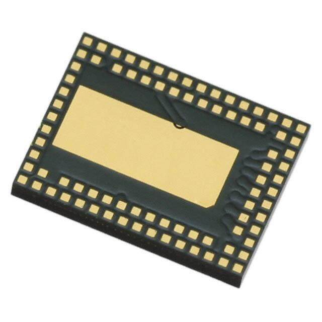
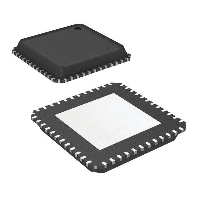
| 描述 | IC TXRX 2.4GHZ-2.5GHZ 48TQFN射频收发器 2.4-2.5GHz 802.11g/b 射频收发器 |
| 产品分类 | RF 收发器集成电路 - IC |
| 品牌 | Maxim Integrated |
| 产品手册 | |
| 产品图片 |
|
| rohs | 符合RoHS无铅 / 符合限制有害物质指令(RoHS)规范要求 |
| 产品系列 | RF集成电路,射频收发器,Maxim Integrated MAX2831ETM+- |
| 数据手册 | |
| 产品型号 | MAX2831ETM+ |
| 产品培训模块 | http://www.digikey.cn/PTM/IndividualPTM.page?site=cn&lang=zhs&ptm=25703http://www.digikey.cn/PTM/IndividualPTM.page?site=cn&lang=zhs&ptm=25705 |
| 产品种类 | 射频收发器 |
| 传输供电电流 | 82 mA |
| 功率-输出 | 18.5dBm |
| 包装 | 托盘 |
| 商标 | Maxim Integrated |
| 天线连接器 | PCB,表面贴装 |
| 存储容量 | - |
| 安装风格 | SMD/SMT |
| 封装 | Tube |
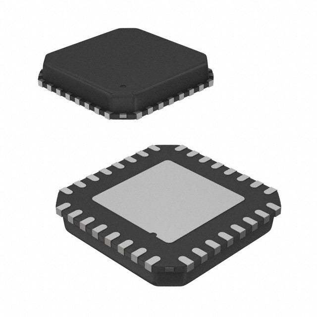
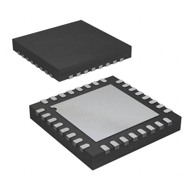
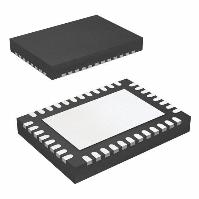
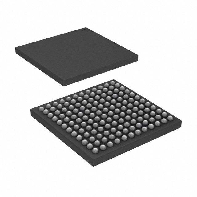
| 封装/外壳 | 48-WFQFN 裸露焊盘 |
| 封装/箱体 | TQFN-EP-48 |
| 工作温度 | -40°C ~ 85°C |
| 工作电源电压 | 2.7 V to 3.6 V, 4.2 V |
| 工厂包装数量 | 43 |
| 应用 | WLAN |
| 应用说明 | 点击此处下载产品Datasheet点击此处下载产品Datasheet点击此处下载产品Datasheet点击此处下载产品Datasheet点击此处下载产品Datasheet点击此处下载产品Datasheet |
| 接口类型 | Parallel, Serial |
| 接收供电电流 | 62 mA |
| 数据接口 | PCB,表面贴装 |
| 数据速率(最大值) | 54Mbps |
| 最大工作温度 | + 85 C |
| 最大数据速率 | 54 Mbps |
| 最小工作温度 | - 40 C |
| 标准包装 | 1 |
| 灵敏度 | - 76 dBm |
| 电压-电源 | 2.7 V ~ 3.6 V |
| 电流-传输 | 209mA |
| 电流-接收 | 62mA |
| 系列 | MAX2831 |
| 调制或协议 | 802.11b/g |
| 调制格式 | OFDM |
| 输出功率 | 18.5 dBm |
| 零件号别名 | MAX2831 |
| 频率 | 2.4GHz ~ 2.5GHz |
| 频率范围 | 2.4 GHz to 2.5 GHz |


- 商务部:美国ITC正式对集成电路等产品启动337调查
- 曝三星4nm工艺存在良率问题 高通将骁龙8 Gen1或转产台积电
- 太阳诱电将投资9.5亿元在常州建新厂生产MLCC 预计2023年完工
- 英特尔发布欧洲新工厂建设计划 深化IDM 2.0 战略
- 台积电先进制程称霸业界 有大客户加持明年业绩稳了
- 达到5530亿美元!SIA预计今年全球半导体销售额将创下新高
- 英特尔拟将自动驾驶子公司Mobileye上市 估值或超500亿美元
- 三星加码芯片和SET,合并消费电子和移动部门,撤换高东真等 CEO
- 三星电子宣布重大人事变动 还合并消费电子和移动部门
- 海关总署:前11个月进口集成电路产品价值2.52万亿元 增长14.8%

PDF Datasheet 数据手册内容提取
19-0363; Rev 2; 3/11 EVAALVUAAILTAIOBNL EKIT 2.4GHz to 2.5GHz 802.11g/b RF Transceivers with Integrated PA General Description Features M The MAX2831/MAX2832 direct conversion, zero-IF, RF ♦ 2.4GHz to 2.5GHz ISM Band Operation A transceivers are designed specifically for 2.4GHz to ♦ IEEE 802.11g/b Compatible (54Mbps OFDM and X 2.5GHz 802.11g/b WLAN applications. The MAX2831 11Mbps CCK) completely integrates all circuitry required to implement 2 the RF transceiver function, providing an RF power ♦ Complete RF Transceiver, PA, and Crystal 8 amplifier (PA), RF-to-baseband receive path, baseband- Oscillator (MAX2831) 3 to-RF transmit path, VCO, frequency synthesizer, crystal Best-in-Class Transceiver Performance 1 oscillator, and baseband/control interface. The MAX2832 62mA Receiver Current integrates the same functional blocks except for the PA. 2.6dB Rx Noise Figure /M Both devices include a fast-settling sigma-delta RF syn- -76dBm Rx Sensitivity (54Mbps OFDM) thesizer with smaller than 20Hz frequency steps and a No I/Q Calibration Required A digitally tuned crystal oscillator allowing use of a low-cost 0.1dB/0.35°Rx I/Q Gain/Phase Imbalance X crystal. The devices also integrate on-chip DC-offset 33dB RF and 62dB Baseband Gain Control cancellation and I/Q errors and carrier leakage-detection 2 Range circuits. Only an RF bandpass filter (BPF), crystal, RF 8 60dB Range Analog RSSI per RF Gain Setting switch, and a small number of passive components are 3 Fast Rx I/Q DC-Offset Settling needed to form a complete 802.11g/b WLAN RF front- Programmable Baseband Lowpass Filter 2 end solution. 20-Bit Sigma-Delta Fractional-N PLL with The MAX2831/MAX2832 completely eliminate the need < 20Hz Step Size for an external SAW filter by implementing on-chip mono- Digitally Tuned Crystal Oscillator lithic filters for both the receiver and transmitter. The +18.5dBm Transmit Power (5.6% EVM with baseband filters are optimized to meet the IEEE 802.11g 54Mbps OFDM) standard and proprietary turbo modes up to 40MHz 31dB Tx Gain Control Range channel bandwidth. These devices are suitable for the full Integrated Power Detector (MAX2831) range of 802.11g OFDM data rates (6Mbps to 54Mbps) Serial or Parallel Gain-Control Interface and 802.11b QPSK and CCK data rates (1Mbps to 11Mbps). The ICs are available in a small, 48-pin TQFN > 40dB Tx Sideband Suppression without package measuring only 7mm x 7mm x 0.8mm. Calibration Tx/Rx I/Q Error Detection Applications ♦ Transceiver Operates from +2.7V to +3.6V Wi-Fi, PDA, VOIP, and Cellular Handsets ♦ PA Operates from +2.7V to +4.2V (MAX2831) Wireless Speakers and Headphones ♦ Low-Power Shutdown Mode General 2.4GHz ISM Radios ♦ Small 48-Pin TQFN Package (7mm x 7mm x 0.8mm) Ordering Information PART TEMP RANGE PIN-PACKAGE MA X 28 3 1 E T M +T -4 0°C to +8 5°C 48 TQFN-E P* MA X 28 3 2 E T M +T -4 0°C to +8 5°C 48 TQFN-E P* *EP=Exposed pad. +Denotes a lead(Pb)-free/RoHS-compliant package. T = Tape and reel. Pin Configuration appears at end of data sheet. ________________________________________________________________Maxim Integrated Products 1 For pricing, delivery, and ordering information,please contact Maxim/Dallas Direct!at 1-888-629-4642, or visit Maxim’s website at www.maxim-ic.com.
2.4GHz to 2.5GHz 802.11g/b RF Transceivers with Integrated PA 2 ABSOLUTE MAXIMUM RATINGS 3 VCCTXPA, VCCPAand TXRF_ to GND....................-0.3V to +4.5V RF Input Power...............................................................+10dBm 8 VCCLNA, VCCTXMX, VCCPLL, VCCCP, VCCXTAL, VCCVCO, Continuous Power Dissipation (TA= +70°C) 2 VCCRXVGA, VCCRXFL, and VCCRXMX_ to GND....-0.3V to +3.9V 48-Pin TQFN (derates 27.8mW/°C above +70°C)..........2.22W B6, B7, B3, B2, SHDN, B5, CS, SCLK, DIN, B1, TUNE, B4, Operating Temperature Range...........................-40°C to +85°C X TXBBI_, TXBBQ_, RXHP, RXTX, RXBBI_, RXBBQ_, RSSI, Junction Temperature......................................................+150°C BYPASS, CPOUT, LD, CLOCKOUT, XTAL, CTUNE, RXRF_ to Storage Temperature Range.............................-65°C to +160°C A GND.......................................-0.3V to (Operating VCC+ 0.3V) Lead Temperature (soldering, 10s).................................+300°C M RXBBI_, RXBBQ_, RSSI, BYPASS, CPOUT, LD, CLOCKOUT Soldering Temperature (reflow).......................................+260°C Short-Circuit Duration..........................................................10s / 1 Stresses beyond those listed under “Absolute Maximum Ratings” may cause permanent damage to the device. These are stress ratings only, and functional 3 operation of the device at these or any other conditions beyond those indicated in the operational sections of the specifications is not implied. Exposure to absolute maximum rating conditions for extended periods may affect device reliability. 8 2 CAUTION! ESD SENSITIVE DEVICE X A DC ELECTRICAL CHARACTERISTICS M (MAX2831 EV kit: VCC_= 2.7V to 3.6V, VCCPA= VCCTXPA= 2.7V to 4.2V, TA= -40°C to +85°C, Rx set to the maximum gain. CS= high, RXHP = SCLK = DIN = low, RSSI and clock output buffer are off, no signal at RF inputs, all RF inputs and outputs terminated into 50Ω, receiver baseband outputs are open. 100mVRMSdifferential I and Q signals (54Mbps IEEE 802.11g OFDM) applied to I/Q baseband inputs of transmitter in transmit mode, fREF= 40MHz, and registers set to recommended settings and corresponding test mode, unless otherwise noted. Typical values are at VCC= 2.8V, VCCPA= 3.3V, and TA= +25°C, LO frequency = 2.437GHz, unless otherwise noted. RF inputs/outputs specifications are referenced to device pins and do not include 1dB loss from EV kit PCB, balun, and SMA connectors.) (Note 1) PARAMETERS CONDITIONS MIN TYP MAX UNITS VCC_ 2.7 3.6 Supply Voltage V VCCPA, VCCTXPA 2.7 4.2 Sh utdo wn mo de , B7: B1 = 0000000, TA = +25°C 20 µA re fere nce oscil la tor not app li e d TA = +25°C 28 35 Standby mode TA = -40°C to +85°C 35 Supply Current TA = +25°C 62 78 Rx mode TA = -40°C to +85°C 82 Tx mode, TA = +25°C, MAX2831, transmit section 82 104 mA VCC = 2.8V, VCCPA = MA X 2831, PA , PO UT = + 18.2dB m 209 258 3.3V, (Note 2) MAX2832 86 Rx calibration mode TA = +25°C 101 Tx calibration mode TA = +25°C 78 Rx I/Q Output Common-Mode TA = +25°C at default common-mode setting 0.98 1.2 1.33 V Voltage Rx I/Q Output Common-Mode TA = -40°C (relative to TA = +25°C) -17 mV Voltage Variation TA = +85°C (relative to TA = +25°C) 15 Tx Baseband Input Common- DC-coupled 0.9 1.3 V Mode Voltage Operating Range Tx Baseband Input Bias Current Source current 22 µA 2 _______________________________________________________________________________________
2.4GHz to 2.5GHz 802.11g/b RF Transceivers with Integrated PA DC ELECTRICAL CHARACTERISTICS (continued) M (MAX2831 EV kit: VCC_= 2.7V to 3.6V, VCCPA= VCCTXPA= 2.7V to 4.2V, TA= -40°C to +85°C, Rx set to the maximum gain. CS= A high, RXHP = SCLK = DIN = low, RSSI and clock output buffer are off, no signal at RF inputs, all RF inputs and outputs terminated into 50Ω, receiver baseband outputs are open. 100mVRMSdifferential I and Q signals (54Mbps IEEE 802.11g OFDM) applied to I/Q X baseband inputs of transmitter in transmit mode, fREF= 40MHz, and registers set to recommended settings and corresponding test 2 mode, unless otherwise noted. Typical values are at VCC= 2.8V, VCCPA= 3.3V, and TA= +25°C, LO frequency = 2.437GHz, unless otherwise noted. RF inputs/outputs specifications are referenced to device pins and do not include 1dB loss from EV kit PCB, balun, 8 and SMA connectors.) (Note 1) 3 PARAMETERS CONDITIONS MIN TYP MAX UNITS 1 LOGIC INPUTS: SHDN, RXTX, SCLK, DIN, CS, B7:B1, RXHP / M VCC - Digital Input-Voltage High, VIH V A 0.4 X Digital Input-Voltage Low, VIL 0.4 V Digital Input-Current High, IIH -1 +1 µA 2 Digital Input-Current Low, IIL -1 +1 µA 8 LOGIC OUTPUTS: LD, CLOCKOUT 3 2 VCC - Digital Output-Voltage High, VOH Sourcing 100µA V 0.4 Digital Output-Voltage Low, VOL Sinking 100µA 0.4 V AC ELECTRICAL CHARACTERISTICS—Rx Mode (MAX2831 EV kit: VCC_= 2.8V, VCCPA= VCCTXPA= 3.3V, TA=+25°C, fRF= 2.439GHz, fLO= 2.437GHz; receiver baseband I/Q out- puts at 112 mVRMS(-19dBV), fREF= 40MHz, SHDN= CS= high, RXTX = SCLK = DIN = low, with power matching for the differential RF pins using the typical applications and registers set to default settings and corresponding test mode, unless otherwise noted. Unmodulated single-tone RF input signal is used with specifications which normally apply over the entire operating conditions, unless otherwise indicated. RF inputs/outputs specifications are referenced to device pins and do not include 1dB loss from EV kit PCB, balun, and SMA connectors.) (Note 1) PARAMETER CONDITIONS MIN TYP MAX UNITS RECEIVER SECTION: LNA RF INPUT-TO-BASEBAND I/Q OUTPUTS RF Input Frequency Range 2.4 2.5 GHz High RF gain 18 RF Input Return Loss Mid RF gain 11 dB Low RF gain 14 Maximum gain, B7:B1 = TA = +25°C 86 98 1111111 TA = -40°C to +85°C 83 Total Voltage Gain dB Minimum gain, B7:B1 = TA = +25°C 3 8 0000000 From high-gain mode (B7:B6 = 11) to medium-gain -16 mode (B7:B6 = 10) RF Gain Steps (Note 3) dB From high-gain mode (B7:B6 = 11) to low-gain mode -33 (B7:B6 = 0X) Gain change from high gain to medium gain, high gain to RF Gain-Change Settling Time low, or medium gain to low gain; gain settling to within 0.2 µs ±2dB of steady state; RXHP = 1 _______________________________________________________________________________________ 3
2.4GHz to 2.5GHz 802.11g/b RF Transceivers with Integrated PA 2 AC ELECTRICAL CHARACTERISTICS—Rx Mode (continued) 3 (MAX2831 EV kit: VCC_= 2.8V, VCCPA= VCCTXPA= 3.3V, TA=+25°C, fRF= 2.439GHz, fLO= 2.437GHz; receiver baseband I/Q out- 8 puts at 112 mVRMS(-19dBV), fREF= 40MHz, SHDN= CS= high, RXTX = SCLK = DIN = low, with power matching for the differential RF pins using the typical applications and registers set to default settings and corresponding test mode, unless otherwise noted. 2 Unmodulated single-tone RF input signal is used with specifications which normally apply over the entire operating conditions, unless X otherwise indicated. RF inputs/outputs specifications are referenced to device pins and do not include 1dB loss from EV kit PCB, balun, and SMA connectors.) (Note 1) A PARAMETER CONDITIONS MIN TYP MAX UNITS M From maximum baseband gain (B5:B1 = 11111) to / Baseband Gain Range 55 62 67 dB 1 minimum baseband gain (B5:B1 = 00000) 3 Voltage gain = maximum with B7:B6 = 11 2.6 8 Voltage gain = 50dB with B7:B6 = 11 3.2 DSB Noise Figure dB 2 Voltage gain = 45dB with B7:B6 = 10 16 X Voltage gain = 15dB with B7:B6 = 0X 34 A -19dBVRMS baseband B7:B6 = 11 -41 In-Band Compression Point M output EVM degrades to B7:B6 = 10 -24 dBm Based on EVM 9% B7:B6 = 0X -6 In-Band Output P-1dB Voltage gain = 90dB, with B7:B6 = 11 2.5 VP-P B7:B6 = 11 -12 Out-of-Band Input IP3 (Note 4) B7:B6 = 10 -4 dBm B7:B6 = 0X 24 I/Q Phase Error 1σ variation (without calibration) ±0.35 De gr e es I/Q Gain Imbalance 1σ variation (without calibration) ±0.1 dB RX I/Q Output Load Impedance Minimum differential resistance 10 kΩ (R || C) Maximum differential capacitance 10 pF Tx-to-Rx Conversion Gain for Rx For receiver gain, B7:B1 = 1101111 (Note 5) 0.5 dB I/Q Calibration Gain change from B5:B1 = 10111 to B5:B1 = 00111; gain Baseband VGA Settling Time 0.1 µs settling to within ±2dB of steady state After switching RXHP to logic 0 from initial logic 1, during I/Q Output DC Step when RXHP ideal short sequence data at -55dBm input in AWGN Transitions from 1 to 0 in channel, for -19dBV output; normalized to RMS signal on -5 dBc Presence of 802.11g Short I and Q outputs; transition point varied from 0 to 0.8µs in Sequence steps of 0.1µs After switching RXHP to 0, D13:D12, Register 7 I/Q Output DC Droop ±1 V/s (A3:A0 = 0111) I/Q Static DC Offset RXHP = 1, B7:B1 = 1101110, 1σ variation ±1 mV Spurious Signal Emissions from RF = 1GHz to 26.5GHz -51 dBm LNA input RECEIVER BASEBAND FILTERS Gain Ripple in Passband 10kHz to 8.5MHz at baseband ±1.3 DBP-P G ro up -D ela y Rip pl e i n P assb and 10kHz to 8.5MHz at baseband ±45 nsP-P 4 _______________________________________________________________________________________
2.4GHz to 2.5GHz 802.11g/b RF Transceivers with Integrated PA AC ELECTRICAL CHARACTERISTICS—Rx Mode (continued) M (MAX2831 EV kit: VCC_= 2.8V, VCCPA= VCCTXPA= 3.3V, TA=+25°C, fRF= 2.439GHz, fLO= 2.437GHz; receiver baseband I/Q out- A puts at 112 mVRMS(-19dBV), fREF= 40MHz, SHDN= CS= high, RXTX = SCLK = DIN = low, with power matching for the differential RF pins using the typical applications and registers set to default settings and corresponding test mode, unless otherwise noted. X Unmodulated single-tone RF input signal is used with specifications which normally apply over the entire operating conditions, unless 2 otherwise indicated. RF inputs/outputs specifications are referenced to device pins and do not include 1dB loss from EV kit PCB, balun, and SMA connectors.) (Note 1) 8 3 PARAMETER CONDITIONS MIN TYP MAX UNITS 1 At 8.5MHz 3.2 / Baseband Filter Rejection At 15MHz 27 M dB (Nominal Mode) At 20MHz 50 A At > 40MHz 80 X RSSI 2 RSSI Minimum Output Voltage RLOAD ≥ 10kΩ || 5pF 0.4 V 8 RSSI Maximum Output Voltage RLOAD ≥ 10kΩ || 5pF 2.4 V 3 RSSI Slope 30 mV/dB 2 To within 3dB of steady +32dB signal step 200 RSSI Output Settling Time ns state -32dB signal step 600 _______________________________________________________________________________________ 5
2.4GHz to 2.5GHz 802.11g/b RF Transceivers with Integrated PA 2 AC ELECTRICAL CHARACTERISTICS—Tx Mode 3 (MAX2831 EV kit: VCC_= 2.8V, VCCPA= VCCTXPA= 3.3V, TA= +25°C, fRF= 2.439GHz , fLO= 2.437GHz. fREF= 40MHz, SHDN= 8 RXTX = CS = high, and SCLK = DIN = low, with power matching for the differential RF pins using the typical applications circuit. 100mVRMSsine and cosine signal (or 100mVRMS54Mbps IEEE 802.11g I/Q signals wherever OFDM is mentioned) applied to base- 2 band I/Q inputs of transmitter (differential DC-coupled). Registers set to recommend settings and corresponding test mode, unless X otherwise noted. RF inputs/outputs specifications are referenced to device pins and do not include 1dB loss from EV kit PCB, balun, and SMA connectors.) (Note 1) A M PARAMETER CONDITIONS MIN TYP MAX UNITS TRANSMIT SECTION: Tx BASEBAND I/Q INPUTS TO RF OUTPUTS / 1 RF Output Frequency Range 2.4 2.5 GHz 3 Output power adjusted 8 54Mbps 802.11g to meet 5.6% EVM, 18.5 2 OFDM signal and spectral mask X B6:B1 = 000000 -7.5 A MAX2831 Output Power 802.11b signal, dBm M 141mVRMS, Output power adjusted 21 IEEE802.11b I/Q to meet spectral mask signals -3dB VGA back off -5.3 MAX2832 B6:B1 = 000000 -31.5 Un w anted Si d eba nd Su pp r e ssio n Without I/Q calibration, B6:B1 = 100001 -42 dBc Carrier Leakage at Center Without DC offset correction -30 dBc Frequency of Channel 1/3 x fLO -67 < 1GHz -36 > 1GHz -47 2/3 x fLO -64 Transmitter Spurious Signal B6:B1 = 111000, dBm/ 4/3 x fLO -42 Emissions (MAX2831) OFDM signal MHz 5/3 x fLO -65 8/3 x fLO -51 2 x fLO -33 3 x fLO -54 1/3 x fLO -78 < 1GHz -65 > 1GHz -72 2/3 x fLO -78 Transmitter Spurious Signal B6:B1 = 111111, dBm/ 4/3 x fLO -46 Emissions (MAX2832) OFDM signal MHz 5/3 x fLO -72 8/3 x fLO -46 2 x fLO -60 3 x fLO -75 6 _______________________________________________________________________________________
2.4GHz to 2.5GHz 802.11g/b RF Transceivers with Integrated PA AC ELECTRICAL CHARACTERISTICS—Tx Mode (continued) M (MAX2831 EV kit: VCC_= 2.8V, VCCPA= VCCTXPA= 3.3V, TA= +25°C, fRF= 2.439GHz , fLO= 2.437GHz. fREF= 40MHz, SHDN= A RXTX = CS = high, and SCLK = DIN = low, with power matching for the differential RF pins using the typical applications circuit. 100mVRMSsine and cosine signal (or 100mVRMS54Mbps IEEE 802.11g I/Q signals wherever OFDM is mentioned) applied to base- X band I/Q inputs of transmitter (differential DC-coupled). Registers set to recommend settings and corresponding test mode, unless 2 otherwise noted. RF inputs/outputs specifications are referenced to device pins and do not include 1dB loss from EV kit PCB, balun, and SMA connectors.) (Note 1) 8 3 PARAMETER CONDITIONS MIN TYP MAX UNITS 1 O ff-c hi p b al un + ma tch, sin g l e- MAX2831 -20 RF Output Return Loss dB / end ed MAX2832 -10 M Tx I/Q Input Load Impedance Minimum differential resistance 20 kΩ A (R || C) Maximum differential capacitance 0.7 pF X Baseband -3dB Corner D1:D0 = 01, Register 8 Nominal mode 11 MHz 2 Frequency (A3:A0 = 1000) 8 Baseband Filter Rejection At 30MHz, in nominal mode 62 dB 3 Minimum Power Detector Output Short sequence transmitter power = +9dBm 0.3 V 2 Voltage Maximum Power Detector Output Short sequence transmitter power = +19dBm 1.2 V Voltage RF Po we r De tector Respo nse Tim e 0.3 µs TRANSMITTER LO LEAKAGE AND I/Q CALIBRATION USING LO LEAKAGE AND SIDEBAND DETECTOR (see the Tx/Rx Calibration Mode section) Tx BASEBAND I/Q INPUTS TO RECEIVER OUTPUTS Output at 1 x fTONE (for LO leakage = -29dBc), -34 Calibration register, LO Leakage and Sideband fTONE = 2MHz, 100mVRMS D12:D11 = 00, dB V RMS Detector Output A3:A0 = 0110 Output at 2 x fTONE (for LO leakage = -240dBc), -44 fTONE = 2MHz, 100mVRMS Amplifier Gain Range D12:D11 = 00 to D12:D11 = 11, A3:A0 = 0110 30 dB Lower -3dB Corner Frequency 1 MHz _______________________________________________________________________________________ 7
2.4GHz to 2.5GHz 802.11g/b RF Transceivers with Integrated PA 2 AC ELECTRICAL CHARACTERISTICS—Frequency Synthesis 3 (MAX2831 EV kit: VCC_= 2.7V, VCCPA= VCCTXPA= 3.3V, TA= +25°C, fLO= 2.437GHz, fREF= 40MHz, SHDN= CS= high, SCLK = 8 DIN = low, PLL loop bandwidth = 150kHz, and TA= +25°C, unless otherwise noted.) (Note 1) 2 PARAMETER CONDITIONS MIN TYP MAX UNITS X FREQUENCY SYNTHESIZER A RF Channel Center Frequency 2.4 2.5 GHz M Channel Center Frequency 20 Hz / Programming Minimum Step Size 1 3 Charge-Pump Comparison 20 MHz 8 Frequency 2 Reference Frequency Range 20 44 MHz X Reference Frequency Input A Levels AC-coupled to XTAL pin 800 mVP-P M Reference Frequency Input Resistance (XTAL) 5 kΩ Impedance (R || C) Capacitance (XTAL) 4 pF fOFFSET = 1kHz -86 fOFFSET = 10kHz -94 Closed-Loop Phase Noise fOFFSET = 100kHz -94 dBc/Hz fOFFSET = 1MHz -110 fOFFSET = 10MHz -120 Closed-Loop Integrated Phase RMS phase jitter; integrate from 10kHz to 10MHz offset 0.9 De g re es Noise Charge-Pump Output Current 1 mA Reference Spurs 20MHz offset -55 dBc M easure d fro m Tx- Rx or Rx- Tx 3µs to 9µs 50 VCO Frequency Error kHz tra nsit i on > 9µs 1 VOLTAGE-CONTROLLED OSCILLATOR Pushing Referred to 2400MHz LO, VCC varies by 0.3V 210 kHz VCO Tuning Voltage Range 0.5 2.2 V LO Tuning Gain VTUNE = 0.5V 1 03 MHz/V VTUNE = 2.2V 8 6 8 _______________________________________________________________________________________
2.4GHz to 2.5GHz 802.11g/b RF Transceivers with Integrated PA AC ELECTRICAL CHARACTERISTICS—Miscellaneous Blocks M (MAX2831 EV kit: VCC_= 2.8V, VCCPA= VCCTXPA= 3.3V, fLO= 2.437GHZ, fREF= 40MHz, SHDN= CS= high, SCLK = DIN = low, A and TA= +25°C, unless otherwise noted.) (Note 1) X PARAMETER CONDITIONS MIN TYP MAX UNITS 2 CRYSTAL OSCILLATOR 8 On-Chip Tuning Capacitance Ma xim u m capa cit ance, A3:A0 = 1110, D6 :D 0 = 1111111 15.4 pF 3 Range M in im um capa cit ance, A3:A0 = 1110, D6 :D 0 = 0000000 0.5 1 On-Chip Tuning Capacitance 0.12 pF / Step Size M ON-CHIP TEMPERATURE SENSOR A TA = -40°C 0.35 X Output Voltage A3:A0 = 1000, D9 :D8 = 01 TA = +25°C 1 V 2 TA = +85°C 1.6 8 3 2 AC ELECTRICAL CHARACTERISTICS—Timing (MAX2831 EV kit: VCC_= 2.8V, VCCPA= VCCTXPA= 3.3V, TA=+25°C, fLO= 2.437GHz, fREF= 40MHz, SHDN= CS= high, SCLK = DIN = low, PLL loop bandwidth = 150kHz, and TA= +25°C, unless otherwise noted.) (Note 1) PARAMETER CONDITIONS MIN TYP MAX UNITS SYSTEM TIMING (See Figure 3) From SHDN rising edge to LO settled within 1kHz using Turn-On Time 60 µs external reference frequency input Crystal Oscillator Turn-On Time 90% of final output amplitude level 1 ms Channel Switching Time Loop BW = 150kHz, fRF = 2.5GHz to 2.4GHz 25 µs Measured from Tx or Rx Rx to Tx 2 enable rising edge; signal Rx/Tx Turnaround Time µs settling to within ±2dB of steady state Tx to Rx, RXHP = 1 2 Tx Turn-On Time (from Standby From Tx-enable active rising edge; signal settling to 1.5 µs Mode) within ±2dB of steady state Tx Turn-Off Time (from Standby From Tx-enable inactive rising edge 1 µs Mode) Rx Turn-On Time (from Standby From Rx-enable active rising edge; signal settling to 1.9 µs Mode) within ±2dB of steady state Rx Turn-Off Time (from Standby From Rx-enable inactive rising edge 0.1 µs Mode) _______________________________________________________________________________________ 9
2.4GHz to 2.5GHz 802.11g/b RF Transceivers with Integrated PA 2 AC ELECTRICAL CHARACTERISTICS—Timing (continued) 3 (MAX2831 EV kit: VCC_= 2.8V, VCCPA= VCCTXPA= 3.3V, TA=+25°C, fLO= 2.437GHz, fREF= 40MHz, SHDN= CS= high, SCLK = 8 DIN = low, PLL loop bandwidth = 150kHz, and TA= +25°C, unless otherwise noted.) (Note 1) 2 PARAMETER CONDITIONS MIN TYP MAX UNITS X 3-WIRE SERIAL-INTERFACE TIMING (See Figure 2) A SCLK Rising Edge to CS Falling 6 ns M Edge Wait Time, tCSO Falling Edge of CS to Rising / 6 ns 1 Edge of First SCLK Time, tCSS 3 DIN to SCLK Setup Time, tDS 6 ns 8 DIN to SCLK Hold Time, tDH 6 ns 2 SCLK Pulse-Width High, tCH 6 ns X SCLK Pulse-Width Low, tCL 6 ns A Last Rising Edge of SCLK to M Rising Edge of CS or Clock to 6 ns Load Enable Setup Time, tCSH CS High Pulse Width, tCSW 20 ns Time Between the Rising Edge of CS and the Next Rising Edge of 6 ns SCLK, tCS1 Clock Frequency, fCLK 20 MHz Rise Time, tR 2 ns Fall Time, tF 2 ns Note 1: Min and max limits are guaranteed by test at TA= +25°C and +85°C and guaranteed by design and characterization at TA= -40°C. The power-on register settings are not production tested. Recommended register setting must be loaded after VCCis supplied. Note 2: Guaranteed by design and characterization. Note 3: The nominal part-to-part variation of the RF gain step is ±1dB. Note 4: Two tones at +25MHz and +48MHz offset with -35dBm/tone. Measure IM3 at 2MHz. Note 5: Tx I/Q inputs = 100mVRMS. 10 ______________________________________________________________________________________
2.4GHz to 2.5GHz 802.11g/b RF Transceivers with Integrated PA Typical Operating Characteristics M (MAX2831 EV kit, VCC_= 2.8V, VCCPA= VCCTXPA= 3.3V, TA= +25°C, fLO= 2.437GHz, fREF= 40MHz, SHDN= CS= high, RXHP = A SCLK = DIN = low.) X NOISE FIGURE Rx VOLTAGE GAIN 2 Rx ICC vs. VCC vs. BASEBAND GAIN SETTINGS vs. BASEBAND GAIN SETTING 6667 TA = +85°C MAX2831/32 toc01 344505 LNA = LOW GAIN MAX2831/32 toc02 178900000 LNA = HIGH GAIN MAX2831/32 toc03 831/ 65 30 M 60 I (mA)CC 64 NF (dB) 2205 LNA = MEDIUM GAIN GAIN (dB) 4500 AX 63 TA = +25°C 15 30 LNA = MEDIUM GAIN 2 10 LNA = HIGH GAIN 20 62 TA = -40°C 8 5 10 LNA = LOW GAIN 3 612.7 2.8 2.9 3.0 3.1 3.2 3.3 3.4 3.5 3.6 0 0 2 4 6 8 101214161820222426283032 0 0 2 4 6 8 101214161820222426283032 2 VCC (V) BASEBAND GAIN SETTINGS BASEBAND GAIN SETTINGS Rx IN-BAND OUTPUT P-1dB vs. GAIN Rx EVM vs. PIN Rx EVM vs. VOUT -10 MAX2831/32 toc04 122802 LNLAN =A H =IG MHE GDAIUINM GAIN LNA = LOW GAIN MAX2831/32 toc05 23..50 LPNINA = = - H50IGdHBm GAIN MAX2831/32 toc06 BV)RMS -2 LGNAAIN M SEWDIITUCMH/ HPIOGIHN-T 1146 2.0 T P-1dB (d --43 GLANIAN MSWEDITIUCMH /PLOOIWN-T EVM (%) 1102 EVM (%) 1.5 U 8 P 1.0 OUT -5 6 4 0.5 -6 2 -7 0 0 15 25 35 45 55 75 85 95 -80 -70 -60 -50 -40 -30 -20 -10 0 -29 -27 -25 -23 -21 -19 -17 -15 -13 -11 -9 GAIN (dB) PIN (dBm) VOUT (dBVRMS) OFDM EVM WITH OFDM JAMMER LNA INPUT RETURN LOSS vs. OFFSET FREQUENCY Rx EMISSION SPECTRUM, LNA INPUT vs. RF FREQUENCY EVM (%) 1111116789012345 PIN = -62fdOBFmFSET = f2O5FMFSHETz = 20MHz MAX2831/32 toc07 dBM -1------45678900000000 VCO LEAKAGE 1.5 VCO LEAKAGE 2x VCO LEAKAGE3x VCO 4x VCO LRNBAW = = LM 3OA0XW208k3 G1H/3Az2I tNoc08 RETURN LOSS (dB) ---211-5050 MID GAIN MAX2831/32 toc09 5 T LOW GAIN -110 U 4 NP 3 -120 I -25 HIGH GAIN 2 -130 1 fOFFSET = 40MHz 0 -140 -30 -65 -55 -45 -35 -25 DC 26.5GHz 2300 2350 2400 2450 2500 2550 2600 PJAMMER (dBm) RF FREQUENCY (MHz) ______________________________________________________________________________________ 11
2.4GHz to 2.5GHz 802.11g/b RF Transceivers with Integrated PA 2 Typical Operating Characteristics (continued) 3 (MAX2831 EV kit, VCC_= 2.8V, VCCPA= VCCTXPA= 3.3V, TA= +25°C, fLO= 2.437GHz, fREF= 40MHz, SHDN= CS= high, RXHP = 8 SCLK = DIN = low.) 2 Rx RSSI STEP RESPONSE Rx RSSI STEP RESPONSE X Rx RSSI OUTPUT vs. INPUT POWER (+32dB LNA GAIN STEP) (-32dB LNA GAIN STEP) MA 23..50 LNA = HIGH GAIN MAX2831/32 toc10 3V MAX2831/32 toc11 3V MAX2831/32 toc12 / 1 V) 2.0 LNA = MEDIUM GAIN 3 UT ( 8 UTP 1.5 0 0V O 2 RSSI 1.0 1.45V 1.5V X A 0.5 LNA = LOW GAIN 0.45 M 0 0V -120 -100 -80 -60 -40 -20 0 20 200ns/div 200ns/div PIN (dBm) Rx I/Q DC OFFSET SETTLING RESPONSE Rx I/Q DC OFFSET SETTLING RESPONSE Rx I/Q DC OFFSET SETTLING RESPONSE (+8dB BB VGA GAIN STEP) (-8dB BB VGA GAIN STEP) (-16dB BB VGA GAIN STEP) MAX2831/32 toc13 MAX2831/32 toc14 MAX2831/32 toc15 3V 2.0V 2.5V 0V 0V 0V 10mV 10mV 10mV 5mV 5mV 5mV 0V 0mV 0V 40ns/div 40ns/div 400ns/div Rx I/Q DC OFFSET SETTLING RESPONSE I/Q OUTPUT DC ERROR DROOP Rx BB VGA SETTLING RESPONSE (-32dB BB VGA GAIN STEP) (RxHP = 1→0; 100Hz MODE) (+8 GAIN STEP) MAX2831/32 toc16 MAX2831/32 toc17 MAX2831/32 toc18 3V 3V 3V 0V 0V 0V 0V 10mV -5mV 500mV 0V 5mV -10mV -500mV 0V 400ns/div 20ms/div 40ns/div 12 ______________________________________________________________________________________
2.4GHz to 2.5GHz 802.11g/b RF Transceivers with Integrated PA Typical Operating Characteristics (continued) M (MAX2831 EV kit, VCC_= 2.8V, VCCPA= VCCTXPA= 3.3V, TA= +25°C, fLO= 2.437GHz, fREF= 40MHz, SHDN= CS= high, RXHP = A SCLK = DIN = low.) X Rx BB VGA SETTLING RESPONSE Rx BB VGA SETTLING RESPONSE Rx BB VGA SETTLING RESPONSE 2 (-8 GAIN STEP) (-16 GAIN STEP) (-32 GAIN STEP) 8 MAX2831/32 toc19 MAX2831/32 toc20 MAX2831/32 toc21 3 3V 3V 3V 1 / M A 0V 0V 0V 500mV 500mV 500mV X 0V 0V 0V 2 8 -500mV -500mV -500mV 3 2 40ns/div 40ns/div 40ns/div RF LNA SETTLING RESPONSE RF LNA SETTLING RESPONSE Rx BB FREQUENCY RESPONSE vs. (HIGH TO MEDIUM) (HIGH TO LOW) FINE SETTING (COARSE SETTING = 8.5MHz) MAX2831/32 toc22 MAX2831/32 toc23 20 3V 3V 0 MAX2831/32 toc24 -20 0V 0V dB -40 500mV 500mV -60 0V 0V -80 -500mV -500mV -100 100ns/div 100ns/div 1 10 100 FREQUENCY (MHz) Rx BB FREQUENCY RESPONSE vs. RX BASEBAND FILTER COARSE SETTING (FINE SETTING = 010) GROUP DELAY HISTOGRAM: Rx STATIC DC OFFSET 200 MAX2831/32 toc25 MAX2831/32 toc26 6758 MSSTAEDMA:NP 0:L. 90E7m S7VImZEV: 1006 MAX2831/32 toc27 -20 52 -40 div dB ns/ 39 -60 20 26 -80 -100 13 -120 0 1 10 100 1 12 1σ/div FREQUENCY (MHz) FREQUENCY (MHz) ______________________________________________________________________________________ 13
2.4GHz to 2.5GHz 802.11g/b RF Transceivers with Integrated PA 2 Typical Operating Characteristics (continued) 3 (MAX2831 EV kit, VCC_= 2.8V, VCCPA= VCCTXPA= 3.3V, TA= +25°C, fLO= 2.437GHz, fREF= 40MHz, SHDN= CS= high, RXHP = 8 SCLK = DIN = low.) 2 X HISTOGRAM: Rx GAIN IMBALANCE HISTOGRAM: Rx PHASE IMBALANCE Tx ICC vs. VCC MA 111358 MSSTAEDMA:NP 0:L. 00E6d S4BIdZBE: 951 MAX2831/32 toc28 19154 MSSTAEDMA:N P0L:. 3E01 .S34°I°ZE: 1013 MAX2831/32 toc29 8868 TA = +85°C MAX2831/32 toc30 / TA = +25°C 1 92 76 84 3 A) 8 69 57 (mC C I 82 2 46 38 X 23 19 80 TA = -40°C A M 0 0 78 1σ/div 1σ/div 2.7 2.8 2.9 3.0 3.1 3.2 3.3 3.4 3.5 3.6 VCC (V) HISTOGRAM: Tx SIDEBAND HISTOGRAM: Tx OUTPUT POWER HISTOGRAM: Tx LO LEAKAGE SUPPRESSION VARIATION 4408 MSSTAEDMA:NP 6:L. 3-E31 S3dI.BZ4E5:d 9B9c9 MAX2831/32 toc31 6702 MSSTAEDMA:N P1L:. 9E-4d S2BIdZBEc: 1000 MAX2831/32 toc32 1102 MGTEOVAEM IAANNC A:H D1IE8JVU.5ESd TB5E.m6D% MAX2831/32 toc33 32 48 8 24 36 6 16 24 4 8 12 2 0 0 0 1σ/div 1σ/div 0.1dB/div Tx OUTPUT POWER vs. FREQUENCY (B6:B1 = 111111) Tx OUTPUT POWER vs. GAIN SETTING Tx BASEBAND FREQUENCY RESPONSE (MAX2832 ONLY) (MAX2832 ONLY) --21000 MAX2831/32 toc34 --10..050 MAX2831/32 toc35 -1-050 MAX2831/32 toc36 LTER RESPONSE (dB)----65430000 P (dBm)OUT---221...505 TAT =A -=4 +08°5C°CTA = +25°C P (dBm)OUT ---221505 FI -3.0 -30 -70 -80 -3.5 -35 -90 -4.0 -40 0.1 1 10 100 2.40 2.42 2.44 2.46 2.48 2.50 0 4 8 1216202428323640444852566064 BASEBAND FREQUENCY (MHz) FREQUENCY (GHz) GAIN SETTINGS 14 ______________________________________________________________________________________
2.4GHz to 2.5GHz 802.11g/b RF Transceivers with Integrated PA Typical Operating Characteristics (continued) M (MAX2831 EV kit, VCC_= 2.8V, VCCPA= VCCTXPA= 3.3V, TA= +25°C, fLO= 2.437GHz, fREF= 40MHz, SHDN= CS= high, RXHP = A SCLK = DIN = low.) X EVM vs. Tx OUTPUT POWER 11g SPECTRAL MASK Tx OUTPUT SPURS 2 (MAX2832 ONLY) (MAX2832 ONLY) (MAX2832 ONLY) EVM (%)122223......702570505050 MAX2831/32 toc36a dBm ------543216-9999999 PEVOMUT == 2-.21.21%7dBm MAX2831/32 toc37 dBm -------17654320000000 RFVCO2x RF2x VCO 3x VCO 4x VCO R80B2W.1 =1 g1 MMSAIHXG2zN83A1/3L2 toc38 831/MAX -79 -80 2 1.50 -89 -90 8 1.25 -99 -100 3 1.00 -109 -110 2 -30 -24 -18 -12 -6 0 2387 2407 2427 2447 2467 2487 DC 26.5GHz OUTPUT POWER (dBm) FREQUENCY (MHz) Tx GAIN VARIATION vs. FREQUENCY Tx EVM vs. POUT PA SUPPLY CURRENT vs. POUT (B6:B1 = 101001) 78 VCVCCPCA P=A 3=. 34V.2V MAX2831/32 toc39a A) 225800 MAX2831/32 toc40 TA = -40°C MAX2831/32 toc41 m 6 VCCPA = 3.0V ENT ( 220 TA = +25°C EVM (%) 5 VCCPA = 2.7V PLY CURR 190 1dB/div TA = +85°C 4 UP VCCPA = 4.2V S A P 160 3 VCCPA = 2.7V, 3.0V, 3.3V 2 130 0 2 4 6 8 10 12 14 16 18 20 22 0 2 4 6 8 10 12 14 16 18 20 22 24 2.40 2.42 2.44 2.46 2.48 2.50 POUT (dBm) POUT (dBm) FREQUENCY (GHz) 802.11g POUT vs. GAIN SETTING Tx OUTPUT POWER vs. FREQUENCY 11g SPECTRAL MASK (UPPER GAIN CONTROL RANGE) 1290 GAIN ADJUSTED TO ACHIEVTEA 5 =.6 +%25 E°VCM MAX2831/32 toc42 --21-999 PEVOMUT == 51.86.%64dBm MAX2831/32 toc43 2202 MAX2831/32 toc44 -39 m) m -49 m) 18 P (dBOUT 18 dB --6599 P (dBOUT 16 -79 17 -89 14 TA = +85°C TA = -40°C -99 16 -109 12 2.40 2.42 2.44 2.46 2.48 2.50 2387 2407 2427 2447 2467 2487 40 44 48 52 56 60 64 FREQUENCY (GHz) FREQUENCY (MHz) GAIN SETTINGS ______________________________________________________________________________________ 15
2.4GHz to 2.5GHz 802.11g/b RF Transceivers with Integrated PA 2 Typical Operating Characteristics (continued) 3 (MAX2831 EV kit, VCC_= 2.8V, VCCPA= VCCTXPA= 3.3V, TA= +25°C, fLO= 2.437GHz, fREF= 40MHz, SHDN= CS= high, RXHP = 8 SCLK = DIN = low.) 2 X POWER DETECTOR OVER FREQUENCY POWER DETECTOR OVER SUPPLY VOLTAGE POWER DETECTOR OVER TEMPERATURE 2831/MA WER DETECTOR (V) 0111112.......8024680 fRF = 2.5fGRFH z= 2.4GHz MAX2831/32 toc45 WER DETECTOR (V) 0111112.......8024680 VCCPA = 2.7V, 3.0V MAX2831/32 toc46 WER DETECTOR (V) 0111112.......8024680 TA = +85°C MAX2831/32 toc47 X PO 0.6 PO 0.6 PO 0.6 TA +=2 -54°0C°C, 0.4 0.4 VCCPA = 3.3V, 4.2V 0.4 A 0.2 0.2 0.2 M 0 0 0 0 2 4 6 8 10 12 14 16 18 20 22 0 2 4 6 8 10 12 14 16 18 20 22 0 2 4 6 8 10 12 14 16 18 20 22 OUTPUT POWER (dBm) OUTPUT POWER (dBm) POUT (dBm) PA OUTPUT POWER HISTORGRAM POWER-DETECTOR OUTPUT PA OUTPUT ENVELOPE RESPONSE FOR 1.1V POWER DETECTOR OUTPUT 300mV 20dB GAIN STEP PA ENVELOPE MAX2831/32 toc48 50mV MAX2831/32 toc49 1102 MEAN = 18.5dBm MAX2831/32 toc50 -50mV 8 TX I/Q INPUT -300mV 6 1V 20dBm 4 POWER DETECTOR 0 0V -20dBm PA ENVELOPE 2 0 100ns/div 1µs/div 0.1dB/div PA OUTPUT RETURN LOSS vs. RF FREQUENCY Tx OUTPUT SPURS B) --1150 MAX2831/32 toc51 -11000 RF R80B2W.1 =1M g1A XMS28IHG31zN/32A tLoc52 T RETURN LOSS (d -20 ----54320000 VCO2x RF2x VCO3x RF 4x RF U TP -60 U -25 O -70 -80 -30 -90 2300 2350 2400 2450 2500 2550 2600 DC 26.5GHz RF FREQUENCY (MHz) 16 ______________________________________________________________________________________
2.4GHz to 2.5GHz 802.11g/b RF Transceivers with Integrated PA Typical Operating Characteristics (continued) M (MAX2831 EV kit, VCC_= 2.8V, VCCPA= VCCTXPA= 3.3V, TA= +25°C, fLO= 2.437GHz, fREF= 40MHz, SHDN= CS= high, RXHP = A SCLK = DIN = low.) X LO PHASE NOISE CHANNEL SWITCHING FREQUENCY LO FREQUENCY vs. VTUNE vs. OFFSET FREQUENCY SETTLING (FROM 2500MHz TO 2400MHz) 2 22565000 MAX2831/32 toc53 ---765000 MAX2831/32 toc54 50kHz MAX2831/32 toc55 831 QUENCY (MHz)22455000 (dBc/Hz)NOISE-1--980000 10kHdziv/ /MA LO FRE2400 PHASE --112100 X2 -130 2350 8 -140 3 2300 -150 -50kHz 0.2 0.4 0.6 0.8 1.0 1.2 1.4 1.6 1.8 2.0 2.2 2.4 0.001 0.01 0.1 1 10 0 250µs 2 VTUNE (V) OFFSET FREQUENCY (MHz) PLL SETTLING TIME FROM PLL SETTLING TIME Rx TO Tx TURNAROUND SHUTDOWN TO STANDBY MODE FROM STANDBY TO Tx PLL SETTLING TIME 50kHz MAX2831/32 toc56 50kHz MAX2831/32 toc57 25kHz MAX2831/32 toc58 10kHz/ 10kHz/ 5kHz/ div div div -50kHz -50kHz -25kHz 0 2ms 0 30µs 0 50µs CRYSTAL-OSCILLATOR OFFSET FREQUENCY Tx-Rx TURNAROUND PLL SETTLING TIME CLOCK OUTPUT vs. CRYSTAL-OSCILLATOR TUNING BITS 25kHz MAX2831/32 toc59 fCCLLOOACDK == 54p0FMHz MAX2831/32 toc60 Y (Hz) 456780000000000 K(CYXO-C32E2R5ASB) MAX2831/32 toc61 C 3V EN 300 U 200 Q RE 100 5kHz/div T F 0 SE-100 F F-200 O 0V AL -300 ST-400 RY-500 C-600 -700 -25kHz -800 0 50µs 10ns/div 0 10 20 30 40 50 60 70 80 90100110120130 CTUNE (DIGITAL BITS) ______________________________________________________________________________________ 17
2.4GHz to 2.5GHz 802.11g/b RF Transceivers with Integrated PA 2 Block Diagrams/Typical Operating Circuits 3 8 2 RX BASEBAND HPF X MODE CORNER FREQUENCY CONTROL TX INPUT CONTROL RX I OUTPUTS A M / 31 RXTX GNDTEST VCCRXMX TXBBI+ TXBBI- TXBBQ+ TXBBQ- VCCRXFL RXHP VCCRXVGA RXBBI+ RXBBI- 8 48 47 46 45 44 43 42 41 40 39 38 37 2 VCCLNA 1 MUX 36 RXBBQ+ X RX Q GNDRXLNA MAX2831 RXBBQ- OUTPUTS A 2 TO 35 RX/TX B6 RSSI RMSUSXI MUX B4 RX/TX GAIN M RX INPUT GAIN CONTROL 3 34 CONTROL RXRF+ BYPASS 4 33 RXRF- TUNE 5 90° 32 RX GAIN B7 GNDVCO 6 31 CONTROL IMUX QMUX 0° VCCPA 7 PLL 30 VCCVCO TX OUTPUT RXC/OTXN TGRAOINL B3 8 DETAEMCTOR CRYSTAL 29 CTUNE ÷(cid:31) OSCILLATOR/ TXRF+ 9 BUFFER 28 XTAL TEMP TXRF- 10 SENSOR TMOU RXSSI 27 VCCXTAL RX/TX GAIN B2 11 POWER DETECTOR SERIAL 26 GNDCP CONTROL TEMP INTERFACE MODE CONTROL SHDN 12 SENRSSOSRI MRSUSXI ÷(cid:31) 25 VCCCP 13 14 15 16 17 18 19 20 21 22 23 24 VCCTXPA B5 CS RSSI VCCTXMX SCLK DIN VCCPLL CLOCKOUT LD B1 CPOUT RX/TX GAIN REFERENCE RX/TX GAIN CONTROL CLOCK BUFFER CONTROL SERIAL INPUTS OUTPUT NOTE: ALL GROUND (PINS 2, 26, AND 31) AND BYPASS CAPACITORS’ GROUND REQUIRE THEIR OWN VIAS TO GROUND. DO NOT CONNECT THEM TO THE EXPOSED PADDLE GROUND. 18 ______________________________________________________________________________________
2.4GHz to 2.5GHz 802.11g/b RF Transceivers with Integrated PA Block Diagrams/Typical Operating Circuits (continued) M A X RX BASEBAND HPF 2 MODE CORNER FREQUENCY CONTROL TX INPUT CONTROL RX I OUTPUTS 8 3 1 / RXTX GNDTEST VCCRXMX TXBBI+ TXBBI- TXBBQ+ TXBBQ- VCCRXFL RXHP VCCRXVGA RXBBI+ RXBBI- MA 48 47 46 45 44 43 42 41 40 39 38 37 X VCCLNA 1 MUX 36 RXBBQ+ RX Q 2 GNDRXLNA 2 MAX2832 TO 35 RXBBQ- OUTPUTS 8 RSSI RSSI MUX RX/TX B6 MUX B4 RX/TX GAIN 3 RX INPUT GAIN CONTROL 3 34 CONTROL 2 RXRF+ BYPASS 4 33 RXRF- TUNE 5 32 90° RX GAIN B7 GNDVCO 6 31 CONTROL IMUX QMUX 0° VCCPA 7 PLL 30 VCCVCO RX/TX GAIN B3 AM CTUNE TX OUTPUT CONTROL 8 DETECTOR CRYSTAL 29 ÷(cid:31) OSCILLATOR/ TXRF+ 9 BUFFER 28 XTAL TEMP TXRF- 10 SENSOR TMOU RXSSI 27 VCCXTAL RX/TX GAIN B2 11 SERIAL 26 GNDCP CONTROL TEMP INTERFACE MODE CONTROL SHDN 12 SENRSSOSRI MRSUSXI ÷(cid:31) 25 VCCCP 13 14 15 16 17 18 19 20 21 22 23 24 VCCTXPA B5 CS RSSI VCCTXMX SCLK DIN VCCPLL CLOCKOUT LD B1 CPOUT RX/TX GAIN REFERENCE RX/TX GAIN CONTROL CLOCK BUFFER CONTROL SERIAL INPUTS OUTPUT NOTE: ALL GROUND (PINS 2, 26, AND 31) AND BYPASS CAPACITORS’ GROUND REQUIRE THEIR OWN VIAS TO GROUND. DO NOT CONNECT THEM TO THE EXPOSED PADDLE GROUND. ______________________________________________________________________________________ 19
2.4GHz to 2.5GHz 802.11g/b RF Transceivers with Integrated PA 2 Pin Description 3 PIN NAME FUNCTION 8 2 1 VCCLNA LNA Supply Voltage X 2 GNDRXLNA LNA Ground 3 B6 Receiver and Transmitter Gain-Control Logic-Input Bit 6 A 4 RXRF+ LNA Differential Input. Input is internally AC-coupled and matched to 100Ω differential. Connect M 5 RXRF- directly to a 2:1 balun. 1/ 6 B7 Receiver Gain-Control Logic-Input Bit 7 3 7 VCCPA Supply Voltage for Second Stage of Power Amplifier 8 8 B3 Receiver and Transmitter Gain-Control Logic-Input Bit 3 2 9 TXRF+ Power-Amplifier Differential Output for the MAX2831. PA output must be AC-coupled. PA driver X internally AC-coupled differential outputs and matched to 100Ω differential for the MAX2832. Connect 10 TXRF- directly to a 2:1 balun. A 11 B2 Receiver and Transmitter Gain-Control Logic-Input Bit 2 M 12 SHDN Active-Low Shutdown and Standby Logic Input. See Table 31 for operating modes. 13 VCCTXPA Supply Voltage for First-Stage of PA and PA Driver 14 B5 Receiver and Transmitter Gain-Control Logic-Input Bit 5 15 CS Active-Low Chip-Select Logic Input of 3-Wire Serial Interface (See Figure 2) 16 RSSI RSSI, PA Power Detector (MAX2831 Only) or Temperature-Sensor Multiplexed Analog Output 17 VCCTXMX Transmitter Upconverter Supply Voltage 18 SCLK Serial-Clock Logic Input of 3-Wire Serial Interface (See Figure 2) 19 DIN Data Logic Input of 3-Wire Serial Interface (See Figure 2) 20 VCCPLL PLL and Registers Supply Voltage. Connect to the supply voltage to retain the register settings. 21 CLOCKOUT Reference Clock Buffer Output Lock-D e tect Logi c Outpu t of Fre qu ency S ynthesiz er. Ou tp ut hi gh in d ic ates that the fre qu ency synthesi zer 22 LD is l ocked. Ou tp ut pr ogr amm ab le as CM OS or op en- dr a in outpu t. (S ee Tabl e s 16 and 20.) 23 B1 Receiver and Transmitter Gain-Control Logic-Input Bit 1 Charge-Pump Output. Connect the frequency synthesizer’s loop filter between CPOUT and TUNE 24 CPOUT (see the Block Diagrams/Typical Operating Circuits). 25 VCCCP PLL Charge-Pump Supply Voltage 26 GNDCP Charge-Pump Circuit Ground 27 VCCXTAL Crystal Oscillator Supply Voltage 28 XTAL Crystal or Reference Clock Input. AC-couple a crystal or a reference clock to this analog input. Connection for Crystal Oscillator Off-Chip Capacitors. When using an external reference clock input, 29 CTUNE leave CTUNE unconnected. 30 VCCVCO VCO Supply Voltage 31 GNDVCO VCO Ground 32 TUNE VCO TUNE Input (see the Block Diagrams/Typical Operating Circuits) On-Chip VCO Regulator Output Bypass. Bypass with a 0.1µF to 1µF capacitor to GND. Do not 33 BYPASS connect other circuitry to this point. 34 B4 Receiver and Transmitter Gain-Control Logic-Input Bit 4 20 ______________________________________________________________________________________
2.4GHz to 2.5GHz 802.11g/b RF Transceivers with Integrated PA Pin Description (continued) M PIN NAME FUNCTION A 35 RXBBQ- Receiver Baseband Q-Channel Differential Outputs. In TX calibration mode, these pins are the LO X 36 RXBBQ+ leakage and sideband detector outputs. 2 37 RXBBI- Receiver Baseband I-Channel Differential Outputs. In TX calibration mode, these pins are the LO 8 38 RXBBI+ leakage and sideband detector outputs. 3 39 VCCRXVGA Receiver VGA Supply Voltage 1 40 RXHP Receiver Baseband AC-Coupling High-Pass Corner Frequency Control Logic Input / M 41 VCCRXFL Receiver Baseband Filter Supply Voltage A 42 TXBBQ- Transmitter Baseband I-Channel Differential Inputs X 43 TXBBQ+ 44 TXBBI- 2 Transmitter Baseband Q-Channel Differential Inputs 45 TXBBI+ 8 3 46 VCCRXMX Receiver Downconverters Supply Voltage 2 47 GNDTEST Connect to Ground 48 RXTX RX/TX Mode Control Logic Input. See Table 31 for operating modes. Exposed Paddle. Connect to the ground plane with multiple vias for proper operation and heat — EP dissipation. Do not share with any other pin grounds and bypass capacitors' ground. Detailed Description LNA Input Matching The LNA features a differential input that is internally The MAX2831/MAX2832 single-chip, low-power, direct AC-coupled and internally matched to 100Ω. Connect a conversion, zero-IF transceivers are designed to support 2:1 balun transformer directly to the RXRF+ (pin 4) and 802.11g/b applications operating in the 2.4GHz to RXRF- (pin 5) ports to convert the differential 100Ω 2.5GHz band. The fully integrated transceivers include a input impedance to a single-ended 50Ω input. Provide receive path, transmit path, voltage-controlled oscillator electrically symmetrical input traces from the LNA input (VCO), sigma-delta fractional-N synthesizer, crystal oscil- to the balun to maintain IP2 performance and RF com- lator, RSSI, PA power detector (MAX2831), temperature mon-mode noise rejection. sensor, Rx and Tx I/Q error-detection circuitry, baseband- control interface and linear power amplifier (MAX2831). LNA Gain Control The only additional components required to implement a The LNA has three gain modes: max gain, max gain - complete radio front-end solution are a crystal, a pair of 16dB, and max gain - 33dB. The three LNA gain modes baluns, a BPF, a switch, and a small number of passive can be serially programmed through the SPI™ interface components (RCs, no inductors required). by programming bits D6:D5 in Register 11 (A3:A0 = 1011) or programmed in parallel through the digital Receiver logic gain-control pins, B7 (pin 6) and B6 (pin 3). Set The fully integrated receiver achieves a noise figure of bit D12 = 1 in Register 8 (A3:A0 = 1000) to enable pro- 2.6dB in high-gain mode, and an input compression point gramming through the SPI interface, or set bit D12 = 0 of -6dBm in low-gain mode, while consuming only 62mA to enable parallel programming. See Table 1 for LNA of supply current. The receiver integrates an LNA and gain-control settings. VGA with a 95dB digitally programmable gain control range, direct-conversion downconverters, I/Q baseband Table 1. LNA Gain-Control Settings (Pins lowpass filters with programmable LPF corner frequen- B7:B6 or Register A3:A0 = 1011, D6:D5) cies, analog RSSI and integrated DC-offset correction cir- cuitry. A logic-low on the RXTX input (pin 48) and a B7 OR D6 B6 OR D5 NAME DESCRIPTION logic-high on the SHDNinput (pin 12) enable the receiver. 1 1 High Max gain 1 0 Medium Max gain - 16dB (typ) 0 X Low Max gain - 33dB (typ) SPI is a trademark of Motorola, Inc. ______________________________________________________________________________________ 21
2.4GHz to 2.5GHz 802.11g/b RF Transceivers with Integrated PA 2 Baseband Variable-Gain Amplifier Baseband Highpass Filter The receiver baseband variable-gain amplifiers provide and DC Offset Correction 3 62dB of gain control range programmable in 2dB steps. The receiver implements programmable AC and near- 8 The VGA gain can be serially programmed through the DC coupling of I/Q baseband signals. Temporary AC- 2 SPI interface by setting bits D4:D0 in Register 11 (A3:A0 coupling is used to quickly remove LO leakage and X = 1011) or programmed in parallel through the digital other DC offsets that could saturate the receiver out- A logic gain-control pins, B5 (pin 14), B4 (pin 34), B3 (pin puts. When DC offsets have settled, near DC-coupling 8), B2 (pin 11), and B1 (pin 23). Set bit D12 = 1 in is enabled to avoid attenuation of the received signal. M Register 8 (A3:A0 = 1000) to enable serial programming AC-coupling is set (-3dB highpass corner frequency of through the serial interface or set bit D12 = 0 to enable 600kHz) when a logic-high is applied to RXHP (pin 40). / 1 parallel programming through the external logic pins. Near DC-coupling is set (-3dB highpass corner fre- 3 See Table 2 for the gain-step value and Table 3 for quency of 100Hz nominal) when a logic-low is applied 8 baseband VGA gain-control settings. to RXHP. Bits D13:D12 in Register 7 (A3:A0 = 0111) allow the near DC-coupling -3B highpass corner fre- 2 Receiver Baseband Lowpass Filter quency to be set to 100Hz (D13:D12 = 00), 4kHz X The receiver integrates lowpass filters that provide an (D13:D12 = X1), or 30kHz (D13:D12 = 10). See Table 6. upper -3dB corner frequency of 8.5MHz (nominal mode) A with 50dB of attenuation at 20MHz, and 45ns of group M delay ripple in the passband (10kHz to 8.5MHz). The Table 4. Receiver LPF Coarse -3dB upper -3dB corner frequency is tightly controlled on-chip Corner Frequency Settings in Register and does not require user adjustment. However, provi- (A3:A0 = 1000) sions are made to allow fine tuning of the upper -3dB cor- ner frequency. In addition, coarse frequency tuning -3dB CORNER BITS (D1:D0) MODE allows the -3dB corner frequency to be set to 7.5MHz FREQUENCY (MHz) (11b mode), 8.5MHz (11g mode), 15MHz (turbo 1 mode), 00 7.5 11b and 18MHz (turbo 2 mode) by programming bits D1:D0 01 8.5 11g in Register 8 (A3:A0 = 1000). See Table 4. The coarse 10 15 Turbo 1 corner frequency can be fine-tuned approximately ±10% in 5% steps by programming bits D2:D0 in Register 7 11 18 Turbo 2 (A3:A0 = 0111). See Table 5 for receiver LPF fine -3dB corner frequency adjustment. Table 5. Receiver LPF Fine -3dB Corner Table 2. Receiver Baseband VGA Gain- Frequency Adjustment in Register Step Value (Pins B5:B1 or Register D4:D0, (A3:A0 = 0111) A3:A0 = 1011) % ADJUSTMENT RELATIVE TO BITS (D2:D0) COARSE SETTING PIN/BIT GAIN STEP (dB) 000 90 B1/D0 2 001 95 B2/D1 4 010 100 B3/D2 8 011 105 B4/D3 16 100 110 B5/D4 32 Table 3. Baseband VGA Gain-Control Table 6. Receiver Highpass Filter -3dB Settings in Receiver Gain-Control Register Corner Frequency Programming (Pin B5:B1 or Register D4:D0, A3:A0 = 1011) A3:A0 = 0111, -3dB HIGHPASS CORNER RXHP B5:B1 OR D4:D0 GAIN D13:D12 FREQUENCY (Hz) 11111 Max 1 XX 600k 11110 Max - 2dB 0 00 100 (recommended) 11101 Max - 4dB 0 X1 4k : : 0 10 30k 00000 Min X = Don’t care. 22 ______________________________________________________________________________________
2.4GHz to 2.5GHz 802.11g/b RF Transceivers with Integrated PA Receiver I/Q Baseband Outputs Register 8 (A3:A0 = 1000) and bit D5:D3 in Register 7 M The differential outputs (RXBBI+, RXBBI-, RXBBQ+, (A3:A0 = 0111). The -3dB corner-frequency is tightly con- RXBBQ-) of the baseband amplifiers have a differential trolled on-chip and does not require user adjustment. A output impedance of ~300Ω, and are capable of dri- Additionally, provisions are made to fine tune the -3dB cor- X ving differential loads up to 10kΩ || 10pF. The outputs ner frequency through bits D5:D3 in the Filter are internally biased to a common-mode voltage of Programming register (A3:A0 = 0111). See Tables 8 and 9. 2 1.1V and are intended to be DC-coupled to the in- Table 7. RSSI Pin Truth Table 8 phase (I) and quadrature (Q) analog-to-digital data 3 converter inputs of the accompanying baseband IC. INPUT CONDITIONS 1 Additionally, the common-mode output voltage can be A3:A0 = 1000, A3:A0 = 1000, RSSI OUTPUT / adjusted from 1.1V to 1.4V through programming bits RXHP M D9:D8 D10 D11:D10 in Register 15 (A3:A0 = 1111). X 0 0 No signal A Received Signal-Strength Indicator (RSSI) 00 0 1 RSSI X The RSSI output (pin 16) can be programmed to multi- Temperature 2 plex an analog output voltage proportional to the 01 0 1 received signal strength, the PA output power sensor 8 (MAX2831), or the die temperature. Set bits D9:D8 = 00 Power detector 3 10 0 1 in Register 8 (A3:A0 = 1000) to enable the RSSI output (MAX2831) 2 in receive mode (off in transmit mode). Set bit D10 = 1 00 1 X RSSI to enables the RSSI output when RXHP = 1, and dis- able the RSSI output when RXHP = 0. Set bit D10 = 0 to 01 1 X Temperature enable the RSSI output independent of RXHP. See sensor Table 7 for a summary of the RSSI output versus regis- Power detector ter programming and RXHP. 10 1 X (MAX2831) The received signal strength indicator provides an ana- X = Don’t care. log voltage proportional to the log of the sum of the Table 8. Transmitter LPF Coarse -3dB squares of the I and Q channels, measured after the receive baseband filters and before the variable-gain Corner Frequency Settings in Register amplifiers. The RSSI analog output voltage is propor- (A3:A0 = 1000) tional to the RF input signal level and LNA gain state over a 60dB range, and is not dependent upon VGA BITS (D1:D0) -3dB CORNER MODE gain. See the graph RX RSSI Output vs. Input Power in FREQUENCY (MHz) the Typical Operating Characteristicsfor further details. 00 8 11b Transmitter 01 11 11g The transmitter integrates baseband lowpass filters, 10 16.5 Turbo 1 direct-upconversion mixers, a VGA, a PA driver, and a lin- 11 22.5 Turbo 2 ear RF PA with a power detector (MAX2831). A logic-high Table 9. Transmitter LPF Fine -3dB on the RXTX input (pin 48) and a logic-high on the SHDN input (pin 12) enable the transmitter. Corner Frequency Adjustment in Register (A3:A0 = 0111) Transmitter I/Q Baseband Inputs The differential analog inputs of the transmitter baseband % ADJUSTMENT RELATIVE TO amplifier I/Q inputs (TXBBI+, TXBBI-, TXBBQ+, TXBBQ-) BITS (D5:D3) COARSE SETTING have a differential impedance of 20kΩ || 1pF. The inputs require an input common-mode voltage of 0.9V to 1.3V, 000 90 which is provided by the DC-coupled I and Q DAC out- 001 95 puts of the accompanying baseband IC. 010 100 Transmitter Baseband Lowpass Filtering 011 105 The transmitter integrates lowpass filters that can be 100 110 (11g) tuned to -3dB corner frequencies of 8MHz (11b), 101 115 11MHz (11g), 16.5MHz (turbo 1 mode), and 22.5MHz 101–111 Not used (turbo 2 mode) through programming bits D1:D0 in ______________________________________________________________________________________ 23
2.4GHz to 2.5GHz 802.11g/b RF Transceivers with Integrated PA 2 Transmitter Variable-Gain Amplifier Power-Amplifier Bias, Enable Delay The variable-gain amplifier of the transmitter provides and Output Matching (MAX2831) 3 31dB of gain control range programmable in 0.5dB The MAX2831 integrates a 2-stage PA, providing 8 steps over the top 8dB of the gain control range and in +18.5dBm of output power at 5.6% EVM (54Mbps 2 1dB steps below that. The transmitter gain can be pro- OFDM signal) in 802.11g mode while exceeding the X grammed serially through the SPI interface by setting 802.11g spectral mask requirements. The first and sec- A bits D5:D0 in Register 12 (A3:A0 = 1100) or in parallel ond stage PA bias currents are set through program- through the digital logic gain-control pins B6:B1 (pins ming bits D2:D0 and bits D6:D3 in Register 10 (A3:A0 = M 3, 6, 8, 11, 14, 23, and 34, respectively). Set bit D10 = 1010), respectively. An adjustable PA enable delay, rel- 0 in Register 9 (A3:A0 = 1001) to enable parallel pro- ative to the transmitter enable (RXTX low-to-high transi- / 1 gramming, and set bit D10 = 1 to enable programming tion), can be set from 200ns to 7µs through 3 through the 3-wire serial interface. See Table 10 for the programming bits D13:D10 in Register 10 (A3:A0 = 8 transmitter VGA gain-control settings. 1010). 2 The PA of the MAX2831 has a 100Ω differential output X Table 10. Transmitter VGA Gain-Control that is internally matched. The output has to be AC-cou- A Settings pled using two off-chip 1.5pF capacitors to a 100Ω:50Ω balun. Provide electrically symmetrical traces from the M D5:D0 Or PA output to the balun to present a balanced load and to NUMBER OUTPUT SIGNAL POWER B6:B1 reduce out-of-band spurs. 63 111111 Max Power Detector (MAX2831) 62 111110 Max - 0.5dB The MAX2831 integrates a voltage-peak detector at the 61 111101 Max - 1.0dB PA output and provides an analog voltage proportional to PA output power. See the Power Detector Over : : : Frequency and Power Detector Over Supply Voltage 49 110001 Max - 7dB graphs in the Typical Operating Characteristics. Set bits 48 110000 Max - 7.5dB D9:D8 = 10 in Register 8 (A3:A0 = 1000) to multiplex the 47 101111 Max - 8dB power-detector analog output voltage to the RSSI output (pin 16). 46 101110 Max - 8dB 45 101101 Max - 9dB Synthesizer Programming 44 101100 Max - 9dB The MAX2831/MAX2832 integrate a 20-bit sigma-delta fractional-N synthesizer, allowing the device to achieve : : : excellent phase-noise performance (0.9° RMS from 5 000101 Max - 29dB 10kHz to 10MHz), fast PLL settling times, and an RF fre- 4 000100 Max - 29dB quency step-size of 20Hz. The synthesizer includes a 3 000011 Max - 30dB divide-by-1 or a divide-by-2 reference frequency divider, an 8-bit integer portion main divider with a divi- 2 000010 Max - 30dB sor range programmable from 64 to 255, and a 20-bit 1 000001 Max - 31dB fractional portion main-divider. Bit D2 in Register 5 0 000000 Max - 31dB (A3:A0 = 0101) sets the reference oscillator divider ratio to 1 or 2. Bits D7:D0 in Register 3 (A3:A0 = 0011) set the integer portion of the main divider. The 20-bit frac- Power-Amplifier Driver Output Matching (MAX2832) tional portion of the main-divider is split between two The PA driver of the MAX2832 has a 100Ω differential registers. The 14 MSBs of the fractional portion are set output with on-chip AC-coupling capacitors. Provide in Register 4 (A3:A0 = 0100), and the 6 LSBs of the frac- electrically symmetrical traces to present a balanced tional portion of the main divider are set in Register 3 load to the PA driver output to help maintain driver lin- (A3:A0 = 0011). See Tables 11 and 12. earity and RF common-mode rejection. 24 ______________________________________________________________________________________
2.4GHz to 2.5GHz 802.11g/b RF Transceivers with Integrated PA Calculating Integer and Fractional Divider Ratios LO Frequency Divider = fRF/ fCOMP= 2437MHz / M The desired integer and fractional divider ratios can be 20MHz = 121.85 calculated by dividing the RF frequency (f ) by f . A RF COMP Integer Divider = 121 (d) = 0111 1001 (binary) For nominal 802.11g/b operation, a 40MHz reference X Fractional Divider = 0.85 x (220- 1) = 891289 (decimal) oscillator is divided by 2 to generate a 20MHz compari- = 1101 1001 1001 1001 1001 2 son frequency (f ). The following method can be COMP used when calculating divider ratios supporting various See Table 13 for integer and fractional divider ratios for 8 reference and comparison frequencies: 802.11g/b systems using a 20MHz comparison frequency. 3 1 Table 11. Integer Divider Register (A3:A0 = 0011) / M BIT RECOMMENDED DESCRIPTION A D13:D8 00000 6 LSBs of 20-Bit Fractional Portion of Main Divider X D7:D0 01111001 8-Bit Integer Portion of Main Divider. Programmable from 64 to 255. 2 8 Table 12. Fractional Divider Register (A3:A0 = 0100) 3 BIT RECOMMENDED DESCRIPTION 2 D13:D0 11011001100110 14 MSBs of 20-Bit Fractional Portion of Main Divider Table 13. IEEE 802.11g/b Divider-Ratio Programming Words fRF INTEGER DIVIDER FRACTIONAL DIVIDER (fRF / fCOMP) (MHz) A3:A0 = 0011, D7:D0 A3:A0 = 0100, D13:D0 A3:A0 = 0011, D13:D8 2412 120.6 0111 1000b 2666h 1Ah 2417 120.85 0111 1000b 3666h 1Ah 2422 121.1 0111 1001b 0666h 1Ah 2427 121.35 0111 1001b 1666h 1Ah 2432 121.6 0111 1001b 2666h 1Ah 2437 121.85 0111 1001b 3666h 1Ah 2442 122.1 0111 1010b 0666h 1Ah 2447 122.35 0111 1010b 1666h 1Ah 2452 122.6 0111 1010b 2666h 1Ah 2457 122.85 0111 1010b 3666h 1Ah 2462 123.1 0111 1011b 0666h 1Ah 2467 123.35 0111 1011b 1666h 1Ah 2472 123.6 0111 1011b 2666h 1Ah 2484 124.2 0111 1100b 0CCCh 33h ______________________________________________________________________________________ 25
2.4GHz to 2.5GHz 802.11g/b RF Transceivers with Integrated PA 2 Crystal Oscillator Reference Clock Output Divider/Buffer The crystal oscillator has been optimized to work with The reference oscillator of the MAX2831/MAX2832 has 3 low-cost crystals (e.g., Kyocera CX-3225SB). See Figure a divider and a buffered output for routing the refer- 8 1. The crystal oscillator frequency can be fine tuned ence clock to the accompanying baseband IC. Bit D10 2 through bits D6:D0 in Register 14 (A3:A0 = 1110), which in Register 14 (A3:A0 = 1110) sets the buffer divider to X control the value of C from 0.5pF to 15.4pF in divide by 1 or 2, independent of the divide ratio for the TUNE 0.12pF steps. See the Crystal-Oscillator Offset reference frequency provided to the PLL. Bit B9 in the A Frequency vs. Crystal-Oscillator Tuning Bits graph in the same register enables or disables the reference buffer M Typical Operating Characteristics. The crystal oscillator output. See the Clock Output waveform in the Typical can be used as a buffer for an external reference fre- Operating Characteristics. / 1 quency source. In this case, the reference signal is AC- Loop Filter 3 coupled to the XTAL pin, and capacitors C1 and C2 are The PLL charge-pump output, CPOUT (pin 24), con- 8 not connected. When used as a buffer, the XTAL input nects to an external third-order, lowpass RC loop-filter, pin has to be AC-coupled. The XTAL pin has an input 2 which in turn connects to the voltage tuning input, impedance of 5kΩ || 4pF, (set D6:D0 = 0000000 in X TUNE (pin 32), of the VCO, completing the PLL loop. Register 14 A3:A0 = 1110). The charge-pump output sink and source current is A 1mA, and the VCO tuning gain is 103MHz/V at 0.5V M tune voltage and 86MHz/V at 2.2V tune voltage. The RC loop-filter values have been optimized for a loop band- MAX2831 width of 150kHz, to achieve the desired Tx/Rx turn- MAX2832 around settling time, while maintaining loop stability and good phase noise. Refer to the MAX2831 EV kit XTAL 28 schematic for the recommended loop-filter component C1 values. Keep the line from this pinto the tune input as CTUNE short as possible to prevent spurious pickup. 29 Lock-Detector Output C2 CTUNE 1.35kΩ 5.9kΩ The PLL features a logic lock-detect output. A logic-high indicates the PLL is locked, and a logic-low indicates the PLL is not locked. Bit D5 in Register 5 (A3:A0 = 0101) enables or disables the lock-detect output. Bit FOR EXTERNAL REFERENCE CLOCK SET, C1 = C2 = OPEN D12 in Register 1 (A3:A0 = 0001) configures the lock- detect output as a CMOS or open-drain output. In open- Figure 1. Crystal Oscillator Schematic drain output mode, bit D9 in Register 5 (A3:A0 = 0101) enables or disables an internal 30kΩ pullup resistor from the open-drain output. 26 ______________________________________________________________________________________
2.4GHz to 2.5GHz 802.11g/b RF Transceivers with Integrated PA Programmable Registers and shifted in MSB first and is framed by CS. When CS is M 3-Wire SPI-Interface low, the clock is active, and data is shifted with the ris- A The MAX2831/MAX2832 include 16 programmable, 18- ing edge of the clock. When CS transitions high, the bit registers. The 14 most significant bits (MSBs) are shift register is latched into the register selected by the X used for register data. The 4 least significant bits contents of the address bits. See Figure 2. Only the last 2 (LSBs) of each register contain the register address. 18 bits shifted into the device are retained in the shift 8 See Table 14 for a summary of the registers and rec- register. No check is made on the number of clock ommended register settings. pulses. For programming data words less than 14 bits 3 long, only the required data bits and the address bits 1 Register data is loaded through the 3-wire SPI/ MICROWIRE™-compatible serial interface. Data is need to be shifted, resulting in faster Rx and Tx gain / M control where only the LSBs need to be programmed. MICROWIRE is a trademark of National Semiconductor Corp. A X Table 14. Recommended Register Settings* 2 DATA ADDRESS 8 REGISTER TABLE D13 D12 D11 D10 D9 D8 D7 D6 D5 D4 D3 D2 D1 D0 (A3:A0) 3 0 0 1 0 1 1 1 0 1 0 0 0 0 0 0 0000 15 2 1 0 1 0 0 0 1 1 0 0 1 1 0 1 0 0001 16 2 0 1 0 0 0 0 0 0 0 0 0 0 1 1 0010 17 3 0 0 0 0 0 0 0 1 1 1 1 0 0 1 0011 18 4 1 1 0 1 1 0 0 1 1 0 0 1 1 0 0100 19 5 0 0 0 0 0 0 1 0 1 0 0 1 0 0 0101 20 6 0 0 0 0 0 0 0 1 1 0 0 0 0 0 0110 21 7 0 1 0 0 0 0 0 0 1 0 0 0 1 0 0111 22 8 1 0 0 0 0 0 0 0 1 0 0 0 0 1 1000 23 9 0 0 0 0 1 1 1 0 1 1 0 1 0 1 1001 24 10 0 1 1 1 0 1 1 0 1 0 0 1 0 0 1010 25 11 0 0 0 0 0 0 0 1 1 1 1 1 1 1 1011 26 12 0 0 0 0 0 1 0 1 0 0 0 0 0 0 1100 27 13 0 0 1 1 1 0 1 0 0 1 0 0 1 0 1101 28 14 0 0 0 0 1 1 0 0 1 1 1 0 1 1 1110 29 15 0 0 0 0 0 1 0 1 0 0 0 1 0 1 1111 30 *The power-on register settings are not production tested. Recommended register settings must be loaded after V is supplied. CC DIN BIT 1 BIT 2 BIT 15 BIT 16 BIT 23 BIT 24 SCLK tCH tCS1 tDS tCL CS tCSO tCSS tDH tCSH tCSW Figure 2. 3-Wire SPI Serial-Interface Timing Diagram ______________________________________________________________________________________ 27
2.4GHz to 2.5GHz 802.11g/b RF Transceivers with Integrated PA 2 Table 15. Register 0 (A3:A0 = 0000) 3 DATA BITS RECOMMENDED DESCRIPTION 8 D13:D11 000 Set to recommended value. 2 Fractional-N PLL Mode Enable. Set 1 to enable the fractional-N PLL or set 0 to enable the X D10 1 integer-N PLL. A D9:D0 1101000000 Set to recommended value. M / Table 16. Register 1 (A3:A0 = 0001) 1 3 DATA BITS RECOMMENDED DESCRIPTION 8 D13 0 Set to recommended value. 2 Lock-Detector Output Select. Set to 1 for CMOS Output. Set to 0 for open-drain output. Bit D9 X D12 1 in register (A3:A0 = 0101) enables or disables an internal 30kΩ pullup resistor in open-drain output mode. A M D11:D0 000110011010 Set to recommended value. Table 17. Register 2 (A3:A0 = 0010) DATA BITS RECOMMENDED DESCRIPTION D13:D0 01000000000011 Set to recommended value. This register contains the 8-bit integer portion and 6 LSBs of the fractional portion of the divider ratio of the synthesizer. Table 18. Register 3 (A3:A0 = 0011) BIT RECOMMENDED DESCRIPTION D13:D8 00000 6 LSBs of 20-Bit Fractional Portion of Main Divider D7:D0 01111001 8-Bit Integer Portion of Main Divider. Programmable from 64 to 255. Table 19. Register 4 (A3:A0 = 0100) BIT RECOMMENDED DESCRIPTION D13:D0 11011001100110 14 MSBs of 20-Bit Fractional Portion of Main Divider Table 20. Register 5 (A3:A0 = 0101) BIT RECOMMENDED DESCRIPTION D13:D10 0000 Set to recommended value. Lock-Detect Output Internal Pullup Resistor Enable. Set to 1 to enable internal 30kΩ pullup D9 0 resistor or set to 0 to disable the resistor. Only available when lock-detect, open-drain output is selected (A3:A0 = 0010, D12 = 1). D8:D6 010 Set to recommended value. Lock-Detect Output Enable. Set to 1 to enable the lock-detect output or set to 0 to disable the D5 1 output. The output is high impedance when disabled. D4:D3 00 Set to recommended value. D2 1 Reference Frequency Divider Ratio to PLL. Set to 0 to divide by 1. Set to 1 to divide by 2. D1:D0 00 Set to recommended value. 28 ______________________________________________________________________________________
2.4GHz to 2.5GHz 802.11g/b RF Transceivers with Integrated PA Table 21. Register 6 (A3:A0 = 0110) M DATA BIT RECOMMENDED DESCRIPTION A D13 0 Set to recommended value. X Tx I/Q Calibration LO Leakage and Sideband Detector Gain-Control Bits. D12:D11 = 00: 9dB; 2 D12:D11 00 01 19dB; 10: 29dB; 11: 39dB. 8 D10:D7 0000 Set to recommended value. 3 Power-Detector Enable in Tx Mode. Set to 1 to enable the power detector or set to 0 to 1 D6 1 disable the detector. / M D5:D2 1000 Set to recommended value. A Tx Calibration Mode. Set to 1 to place the device in Tx calibration mode or 0 to place the D1 0 device in normal Tx mode when RXTX is set to 1 (see Table 31). X Rx Calibration Mode. Set to 1 to place the device in Rx calibration mode or 0 to place the 2 D0 0 device in normal Rx mode when RXTX is set to 0 (see Table 31). 8 3 Table 22. Register 7 (A3:A0 = 0111) 2 BIT RECOMMENDED DESCRIPTION Receiver Highpass Corner Frequency Setting for RXHP = 0. Set to 00 for 100Hz, X1 for 4kHz, D13:D12 01 and 10 for 30kHz. D11:D6 000000 Set to recommended value. Transmitter Lowpass Filter Corner Frequency Fine Adjustment (Relative to Coarse Setting). D5:D3 100 See Table 8. Bits D1:D0 in A3:A0 = 1000 provide the lowpass filter corner coarse adjustment. Receiver Lowpass Filter Corner Frequency Fine Adjustment (Relative to Coarse Setting). See D2:D0 010 Table 5. Bits D1:D0 in A3:A0 = 1000 provide the lowpass filter corner coarse adjustment. Table 23. Register 8 (A3:A0 = 1000) BIT RECOMMENDED DESCRIPTION D13 1 Set to recommended value. Enable Receiver Gain Programming Through the Serial Interface. Set to 1 to enable D12 0 programming through the 3-wire serial interface (D6:D0 in Register A3:A0 = 1011). Set to 0 to enable programming in parallel through external digital pins (B7:B1). D11 0 Set to recommended value. RSSI Operating Mode. Set to 1 to enable RSSI output independent of RXHP. Set to 0 to D10 0 disable RSSI output if RXHP = 0, and enable the RSSI output if RXHP = 1. RS SI , Po w er De tector or Temp er atur e Se nsor O utp ut Se l ect. Se t to 00 to enabl e the RS SI D9:D8 00 outp ut in r ecei ve mo d e. S et to 01 to enabl e the temp er atur e sensor outpu t in r ecei ve and tr ansm i t mo d es. Se t to 10 to enabl e the p owe r - d etector outpu t i n tra nsm it m ode . Se e Tab l e 7. D7:D2 001000 Set to recommended value. Receiver and Transmitter Lowpass Filter Corner Frequency Coarse Adjustment. See Tables 4 D1:D0 01 and 7. ______________________________________________________________________________________ 29
2.4GHz to 2.5GHz 802.11g/b RF Transceivers with Integrated PA 2 Table 24. Register 9 (A3:A0 = 1001) 3 BIT RECOMMENDED DESCRIPTION 8 D13:D11 000 Set to recommended value. 2 Enable Transmitter Gain Programming Through the Serial or Parallel Interface. Set to 1 to X D10 0 enable programming through the 3-wire serial interface (D5:D0 in Register A3:A0 = 1011). A Set to 0 to enable programming in parallel through external digital pins (B6:B1). M D9:D0 1110110101 Set to recommended value. / 1 3 8 Table 25. Register 10 (A3:A0 = 1010) 2 BIT RECOMMENDED DESCRIPTION X Po w er- A mp li f ie r En abl e De la y. Se ts a de la y be twe en RXT X l ow- t o- hig h tra nsit io n and in tern al P A D13:D10 0111 A enabl e . Pr o gr a m ma bl e in 0.5µs steps . D1 3:D1 0 = 0001 (0 .2µs) and D1 3:D1 0 = 1111 (7 µs). M D9:D7 011 Set to recommended value. D6:D3 0100 Second-Stage Power-Amplifier Bias Current Adjustment. Set to XXXX for 802.11g/b. D2:D0 100 First-Stage Power-Amplifier Bias Current Adjustment. Set to XXX for 802.11g/b. Table 26. Register 11 (A3:A0 = 1011) BIT RECOMMENDED DESCRIPTION D13:D7 0000000 Set to recommended value. LNA Gain Control. Set to 11 for high-gain mode. Set to 10 for medium-gain mode, reducing D6:D5 11 LNA gain by 16dB. Set to 0X for low-gain mode, reducing LNA gain by 33dB. Receiver VGA Control. Set D4:D0 = 00000 for minimum gain and D4:D0 = 11111 for D4:D0 11111 maximum gain. Table 27. Register 12 (A3:A0 = 1100) BIT RECOMMENDED DESCRIPTION D13:D6 00000101 Set to recommended value. Transmitter VGA Gain Control. Set D5:D0 = 000000 for minimum gain, and set D5:D0 = D5:D0 000000 111111 for maximum gain. Table 28. Register 13 (A3:A0 = 1101) BIT RECOMMENDED DESCRIPTION D13:D10 0011 Set to recommended value. D9:D6 1010 Set to recommended value. D5:D0 010010 Set to recommended value. 30 ______________________________________________________________________________________
2.4GHz to 2.5GHz 802.11g/b RF Transceivers with Integrated PA Table 29. Register 14 (A3:A0 = 1110) M BIT RECOMMENDED DESCRIPTION A D13:D11 000 Set to recommended value. X D10 0 Reference Clock Output Divider Ratio. Set 1 to divide by 2 or set 0 to divide by 1. 2 D9 1 Refere nce Cl o ck Outpu t En ab le . Se t 1 to enabl e the re fere nce cl ock outpu t or set 0 to di s abl e . 8 D8:D7 10 Set to recommended value. 3 D6:D0 XXXXXXX Crystal-Oscillator Fine Tune. Tunes crystal oscillator over ±20ppm to within ±1ppm. 1 X = Don’t care. / M A Table 30. Register 15 (A3:A0 = 1111) X 2 BIT RECOMMENDED DESCRIPTION 8 D13:D12 00 Set to recommended value. 3 Receiver I/Q Output Common-Mode Voltage Adjustment. Set D11:D10 = 00: 1.1V, D11:D10 00 2 01: 1.2V, 10: 1.3V, 11: 1.45V. D9:D0 0101000101 Set to recommended value. Table 31. Operating Mode Table REGISTER LOGIC PINS CIRCUIT BLOCK STATES SETTINGS MODE PLL, VCO, D1:D0 CALIBRATION SHDN RXTX Rx PATH Tx PATH LO GEN, (A3:A0 = 0110) SECTIONS ON AUTO-TUNER Shutdown 0 0 00 Off Off Off None Standby 0 1 00 Off Off On None Rx 1 0 X0 On Off On None Tx 1 1 0X Off On On None On Ca l tone, RF ph ase Rx Calibration 1 0 X1 Upconverters On (except LNA) shi ft, Tx fil t er On (except PA AM detector, Tx Calibration 1 1 1X Off On driver and PA) Rx I/Q buffers X = Don’t care. ______________________________________________________________________________________ 31
2.4GHz to 2.5GHz 802.11g/b RF Transceivers with Integrated PA 2 Modes of Operation The LO leakage and sideband detector output are The modes of operation for the MAX2831/MAX2832 are taken at the receiver I and Q channel outputs during 3 shutdown, standby, transmit, receive, transmitter calibra- this calibration phase. 8 tion, and receiver calibration. See Table 31 for a summa- During Tx LO leakage and I/Q imbalance calibration, a 2 ry of the modes of operation. The logic-input pins, SHDN sine and cosine signal (f = f ) is input to the base- X (pin 12) and RXTX (pin 48), control the various modes. TONE band I/Q Tx pins from the baseband IC. At the LO leak- A age and sideband-detector output, the LO leakage Shutdown Mode corresponds to the signal at f and the sideband M The MAX2831/MAX2832 feature a low-power shutdown TONE suppression corresponds to the signal at 2 x f . The mode that disables all circuit blocks, except the serial- TONE / output power of these signals vary 1dB for 1dB of varia- 1 interface and internal registers, allowing the registers to tion in the LO leakage and sideband suppression. To be loaded and values maintained, as long as V is 3 CC calibrate the Tx path, first set the power-detector gain applied. Set SHDN and RXTX logic-low to place the 8 to 9dB using D12:D11 in Register 5 (see Table 21). device in shutdown mode. 2 Adjust the DC offset of the baseband inputs to minimize X After supply voltage ramp up, supply current in shut- the signal at fTONE(LO leakage). Then, adjust the base- down mode could be high. Program the default value to band input relative magnitude and phase offsets to A SPI register 0 to eliminate high shutdown current. reduce the signal at 2 x f . TONE M Standby Mode In Rx calibration mode, the calibrated Tx RF signal is The standby mode is used to enable the frequency internally routed to the Rx inputs. In this mode, the synthesizer block while the rest of the device is pow- VCO/LO generator/PLL blocks are powered on and ered down. In this mode, the PLL, VCO, and LO gener- active except for the low-noise amplifier (LNA). ators are on, so that Tx or Rx modes can be quickly Applications Information enabled from this mode. Set SHDN to a logic-low and RXTX to a logic-high to place the device in standby Layout Issues mode. The MAX2831 EV kit can be used as a starting point for layout. For best performance, take into consideration Receive (Rx) Mode grounding and RF, baseband, and power-supply rout- The complete receive signal path is enabled in this ing. Make connections from vias to the ground plane as mode. Set SHDNto logic-high and RXTX to logic-low to short as possible. Do not connect the device ground place the device in Rx mode. pin to the exposed paddle ground. Keep the buffered Transmit (Tx) Mode clock output trace as short as The complete transmitter signal path is enabled in this possible. Do not share the trace with the RF input layer, mode. Set SHDN and RXTX to logic-high to place the especially on or inter-layer or back side of the board. device in Tx mode. On the high-impedance ports, keep traces short to min- imize shunt capacitance. EV kit Gerber files can be Tx/Rx Calibration Mode requested at www.maxim-ic.com. The MAX2831/MAX2832 feature Rx/Tx calibration modes to detect I/Q imbalances and transmit LO leakage. In the Power-Supply Layout Tx calibration mode, all Tx circuit blocks, except the PA To minimize coupling between different sections of the driver and external PA, are powered on and active. The IC, a star power-supply routing configuration with a AM detector and receiver I and Q channel buffers are large decoupling capacitor at a central VCCnode is rec- also on, along with multiplexers in the receiver side to ommended. The VCC traces branch out from this node, route this AM detector’s signal. In this mode, the LO each going to a separate VCC node in the circuit. Place leakage calibration is done only for the LO leakage sig- a bypass capacitor as close as possible to each supply nal that is present at the center frequency of the channel pin. This arrangement provides local decoupling at (i.e., in the middle of the OFDM or QPSK spectrum). The each VCCpin. Use at least one via per bypass capacitor LO leakage calibration includes the effect of all DC off- for a low-inductance ground connection. Do not share sets in the entire baseband paths of the I/Q modulator the capacitor ground vias with any other branch and the and direct leakage of the LO to the I/Q modulator output. exposed paddle ground. 32 ______________________________________________________________________________________
2.4GHz to 2.5GHz 802.11g/b RF Transceivers with Integrated PA M POWER SUPPLY A ON POWER 3-WIRE SERIAL INTERFACE AVAILABLE X 2 IREF 8 3 1 SHDN SHUTDOWN / M C A M RXTX 2 A 3 8 2 AX X M 31/ 2 8 2 X 8 CS A CS (SELECT) M 3 SPI SCLK SCLK (CLOCK) 2 C A M DIN DIN (DATA) SPI: CHANNEL FREQUENCY, PA BIAS, TRANSMITTER LINEARITY, RECEIVER RSSI OPERATION, CALIBRATION MODE, ETC. INTERNAL PA ENABLED (DRIVES POWER RAMP CONTROL) 0 TO 7µs PA ENABLE SHUTDOWN STANDBY RECEIVE TRANSMIT MODE MODE MODE MODE Figure 3. Timing Diagram Pin Configuration Chip Information PROCESS: BiCMOS TOP VIEW RXTX GNDTEST VCCRXMX TXBBI+ TXBBI- TXBBQ+ TXBBQ- VCCRXFL RXHP VCCRXVGA RXBBI+ RXBBI- 48 47 46 45 44 43 42 41 40 39 38 37 Package Information VCCLNA 1 + 36 RXBBQ+ For the latest package outline information and land patterns GNDRXLNA 2 35 RXBBQ- (footprints), go to www.maxim-ic.com/packages. Note that a B6 3 34 B4 "+", "#", or "-" in the package code indicates RoHS status only. Package drawings may show a different suffix character, but RXRF+ 4 33 BYPASS the drawing pertains to the package regardless of RoHS status. RXRF- 5 32 TUNE B7 6 MAX2831 31 GNDVCO PACKAGE PACKAGE OUTLINE LAND PATTERN VCCPA 7 MAX2832 30 VCCVCO TYPE CODE NO. NO. B3 8 29 CTUNE 48 TQFN-E P T4877+4 21- 0 14 4 90- 0 13 0 TXRF+ 9 28 XTAL TXRF- 10 27 VCCXTAL B2 11 26 GNDCP SHDN 12 EP 25 VCCCP 13 14 15 16 17 18 19 20 21 22 23 24 VCCTXPA B5 CS RSSI VCCTXMX SCLK DIN VCCPLL CLOCKOUT LD B1 CPOUT TQFN ______________________________________________________________________________________ 33
2.4GHz to 2.5GHz 802.11g/b RF Transceivers with Integrated PA 2 Revision History 3 REVISION REVISION PAGES 8 DESCRIPTION NUMBER DATE CHANGED 2 0 10/06 Initia l rele ase — X 1 3/10 Removed MAX2832 future product reference and made minor corrections 1, 2, 10, 18, 19, 20 A Corrected conditions for Rx I/Q Output Common-Mode Voltage Variation in the M 2, 27, 28, 2 3/11 DC Electrical Characteristics; corrected Tables 14, 17, and 27; added text to 30, 32 / Shutdown Mode section 1 3 8 2 X A M Maxim cannot assume responsibility for use of any circuitry other than circuitry entirely embodied in a Maxim product. No circuit patent licenses are implied. Maxim reserves the right to change the circuitry and specifications without notice at any time. 34 ____________________Maxim Integrated Products, 120 San Gabriel Drive, Sunnyvale, CA 94086 408-737-7600 © 2011 Maxim Integrated Products Maxim is a registered trademark of Maxim Integrated Products, Inc.