ICGOO在线商城 > MAX1273CUA+

 Datasheet下载
- 型号: MAX1273CUA+
- 制造商: Maxim
- 库位|库存: xxxx|xxxx
- 要求:
| 数量阶梯 | 香港交货 | 国内含税 |
| +xxxx | $xxxx | ¥xxxx |
查看当月历史价格
查看今年历史价格
MAX1273CUA+产品简介:
ICGOO电子元器件商城为您提供MAX1273CUA+由Maxim设计生产,在icgoo商城现货销售,并且可以通过原厂、代理商等渠道进行代购。 提供MAX1273CUA+价格参考以及MaximMAX1273CUA+封装/规格参数等产品信息。 你可以下载MAX1273CUA+参考资料、Datasheet数据手册功能说明书, 资料中有MAX1273CUA+详细功能的应用电路图电压和使用方法及教程。
MAX1273CUA+是Maxim Integrated(现属Analog Devices)推出的12位、串行输出、8通道多路复用模数转换器(ADC),采用μMAX-8封装,支持2.7V–3.6V单电源供电,采样速率高达100ksps。其典型应用场景包括:

工业过程控制:用于传感器信号采集(如温度、压力、电流环4–20mA经调理后的电压信号),配合微控制器实现多点数据监测与闭环调节。

便携式仪器仪表:凭借低功耗(待机电流仅1μA)、小尺寸和宽温范围(–40°C至+85°C),适用于手持式万用表、数据记录仪及现场校准设备。

医疗电子:在便携式监护设备(如血糖仪、心率检测模块)中采集生物电信号或传感器模拟量,满足精度(INL ±1 LSB)与稳定性要求。

汽车电子子系统:用于车载环境监测(如舱内温湿度、电池电压/电流采样),符合AEC-Q100可靠性标准(注:MAX1273CUA+为商用级,若需车规应用需确认具体版本或选用对应车规型号)。

此外,其内置基准源(2.048V)、SPI/QSPI兼容接口及通道自动扫描模式,简化了嵌入式系统设计,广泛应用于需要中等精度、多通道、低功耗数据采集的嵌入式终端设备。
| 参数 | 数值 |
| 产品目录 | 集成电路 (IC) |
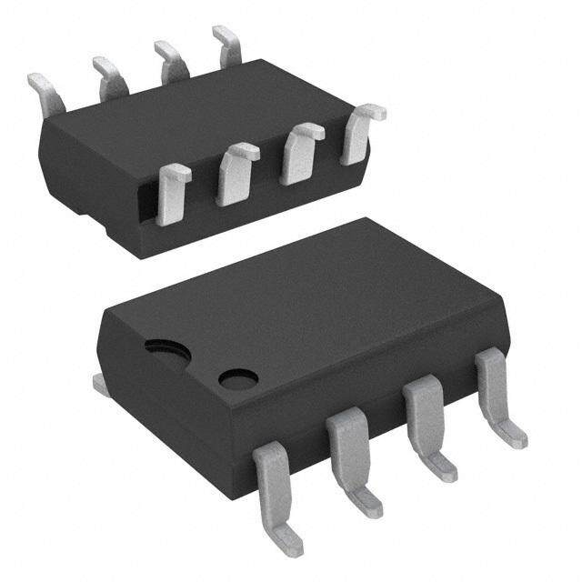
| 描述 | IC ADC 12BIT SRL 87KSPS 8UMAX |
| 产品分类 | |
| 品牌 | Maxim Integrated |
| 数据手册 | |
| 产品图片 |
|
| 产品型号 | MAX1273CUA+ |
| rohs | 无铅 / 符合限制有害物质指令(RoHS)规范要求 |
| 产品系列 | - |
| 位数 | 12 |
| 供应商器件封装 | 8-uMAX |
| 包装 | 管件 |
| 安装类型 | 表面贴装 |
| 封装/外壳 | 8-TSSOP,8-MSOP(0.118",3.00mm 宽) |
| 工作温度 | -40°C ~ 85°C |
| 数据接口 | MICROWIRE™,QSPI™,串行,SPI™ |
| 标准包装 | 1 |
| 特性 | - |
| 电压源 | 单电源 |
| 转换器数 | 1 |
| 输入数和类型 | 1 个单端,单极1 个单端,双极 |
| 采样率(每秒) | 87k |









PDF Datasheet 数据手册内容提取
19-2921; Rev 3; 12/11 EVAALVUAAILTAIOBNL EKIT Fault-Protected, 12-Bit ADCs with Software-Selectable Input Range General Description Features M The MAX1272/MAX1273 multirange 12-bit data-acquisi- (cid:1) Four Software-Selectable Input Ranges A tion systems (DAS) operate with a single 5V supply. The MAX1272: 0 to 10V, 0 to 5V, ±10V, ±5V X software-programmable analog input accepts a variety MAX1273: 0 to VREF, 0 to VREF/2, ±VREF, of voltage ranges: ±10V, ±5V, 0 to 10V, 0 to 5V for the ±VREF/2 1 MAX1272; ±VREF, ±VREF/2, 0 to VREF, 0 to VREF/2 for the (cid:1) 12-Bit Resolution, No Missing Codes 2 MAX1273. The software-selectable extended analog 7 input range increases the effective dynamic range to 14 (cid:1) 5V Single-Supply Operation 2 bits and provides the flexibility to interface 4–20mA pow- (cid:1) SPI/QSPI/MICROWIRE-Compatible 3-Wire ered sensors directly to a single 5V system. In addition, Interface /M the MAX1272 provides fault protection to ±12V. Other features include a 5MHz track/hold (T/H) bandwidth, (cid:1) 87ksps Sampling Rate A 87ksps throughput rate, and internal (4.096V) or external (cid:1) ±12V Fault-Protected Analog Input (MAX1272) X (2.40V to 4.18V) reference. (cid:1) Internal (4.096V) or External (2.4V to 4.18V) 1 The MAX1272/MAX1273 serial interfaces connect Reference 2 directly to SPI/QSPI™/MICROWIRE®-compatible devices without any external logic. (cid:1) Low Power 7 1.5mA at 87ksps 3 Four software-programmable power-down modes 0.4mA at 10ksps (delayed standby, immediate standby, delayed full power- 0.2mA at 1ksps down, and immediate full power-down) provide low-cur- rent shutdown between conversions. In standby mode, the (cid:1) Four Power-Down Modes internal reference buffer remains active, thus eliminating (cid:1) 8-Pin µMAX Package startup delay. The MAX1272/MAX1273 are available in an 8-pin Ordering Information µMAX® package. Both devices are available in the extended (-40°C to +85°C) temperature range. TEMP PIN- INL PART Applications RANGE PACKAGE (LSB) Industrial Control Systems MAX1272EUA+ -40°C to +85°C 8 µMAX ±1 MAX1273EUA+ -40°C to +85°C 8 µMAX ±1 Data-Acquisition Systems +Denotes a lead(Pb)-free/RoHS-compliant package. Robotics Automatic Testing Battery-Powered Instruments Medical Instruments Pin Configuration TOP VIEW + SCLK 1 8 DOUT Typical Application Circuit appears at end of data sheet. DIN 2 7 CS MAX1272 VDD 3 MAX1273 6 REF GND 4 5 AIN QSPI is a trademark of Motorola, Inc. µMAX MICROWIRE is a registered trademark of National Semiconductor Corp. µMAX is a registered trademark of Maxim Integrated Products, Inc. ________________________________________________________________Maxim Integrated Products 1 For pricing, delivery, and ordering information,please contact Maxim Directat 1-888-629-4642, or visit Maxim’s website at www.maxim-ic.com.
Fault-Protected, 12-Bit ADCs with Software-Selectable Input Range 3 ABSOLUTE MAXIMUM RATINGS 7 VDDto GND..............................................................-0.3V to +6V Operating Temperature Ranges 2 AIN to GND (MAX1272)......................................................±12V Storage Temperature Range.............................-65°C to +150°C 1 AIN to GND (MAX1273)........................................................±6V Junction Temperature .....................................................+150°C DOUT, CS, DIN, SCLK, REF to GND..........-0.3V to (VDD+ 0.3V) Lead Temperature (soldering, 10s).................................+300°C X Maximum Current into Any Pin............................................50mA Soldering Temperature (reflow).......................................+260°C A Continuous Power Dissipation (TA= +70°C) µMAX M Single-Layer Board (derate 4.5mW/ C above +70°C).........362mW Multilayer Board (derate 4.8mW/ C above +70°C)...........387.8mW / 2 Stresses beyond those listed under “Absolute Maximum Ratings” may cause permanent damage to the device. These are stress ratings only, and functional 7 operation of the device at these or any other conditions beyond those indicated in the operational sections of the specifications is not implied. Exposure to 2 absolute maximum rating conditions for extended periods may affect device reliability. 1 X ELECTRICAL CHARACTERISTICS A (VDD = 4.75V to 5.25V, unipolar/bipolar input range, external reference mode, VREF = 4.096V, CREF = 1.0µF, fSCLK = 1.4MHz, 50% duty cycle, CLOAD= 50pF, TA= -40°C to +85°C, unless otherwise noted. Typical values are at TA= +25°C.) M PARAMETERS SYMBOL CONDITIONS MIN TYP MAX UNITS ACCURACY (Note 1) Resolution 12 Bits Integral Nonlinearity INL ±0.3 ±1.0 LSB Differential Nonlinearity DNL No missing codes over temperature ±0.35 ±1.00 LSB Unipolar ±7.5 Offset Error LSB Bipolar ±7.5 Unipolar ±5 Gain Error (Note 2) LSB Bipolar ±7 Gain Error Temperature Unipolar ±3 ppm/°C Coefficient (Note 2) Bipolar ±5 DYNAMIC SPECIFICATIONS (10kHz sine-wave input, ±10VP-P (MAX1272), or ±4.096VP-P (MAX1273), fSAMPLE = 87ksps) Signal-to-Noise + Distortion Ratio SINAD 69 72 dB Total Harmonic Distortion THD Up to the 5th harmonic -87 -78 dB Spurious-Free Dynamic Range SFDR 80 88 dB Aperture Delay tAD 15 ns Aperture Jitter tAJ <50 ps ANALOG INPUT T/H Acquisition Time tACQ 2.85 µs 2 _______________________________________________________________________________________
Fault-Protected, 12-Bit ADCs with Software-Selectable Input Range ELECTRICAL CHARACTERISTICS (continued) M (VDD = 4.75V to 5.25V, unipolar/bipolar input range, external reference mode, VREF = 4.096V, CREF = 1.0μF, fSCLK = 1.4MHz, A 50% duty cycle, CLOAD= 50pF, TA= -40°C to +85°C, unless otherwise noted. Typical values are at TA= +25°C.) X PARAMETERS SYMBOL CONDITIONS MIN TYP MAX UNITS 1 ±10V (MAX1272) or ±VREF (MAX1273) 5 2 range 7 ±5V (MAX1272) or ±VREF/2 (MAX1273) 2.5 2 range Small-Signal Bandwidth BW-3dB MHz /M 0 to 10V (MAX1272) or 0 to VREF (MAX1273) 2.5 range A 0 to 5V (MAX1272) or 0 to VREF/2 X 1.25 (MAX1273) range 1 RNG = 1 0 10 MAX1272 2 RNG = 0 0 5 7 Unipolar RNG = 1 0 VREF 3 MAX1273 Input Voltage Range RNG = 0 0 VREF/2 VIN V (Tables 2, 3) RNG = 1 -10 +10 MAX1272 RNG = 0 -5 +5 Bipolar RNG = 1 -VREF +VREF MAX1273 RNG = 0 -VREF/2 +VREF/2 0 to 10V range -10 +860 MAX1272 0 to 5V range -10 +430 Unipolar 0 to VREF range -10 +10 MAX1273 0 to VREF/2 range -10 +10 Input Current IIN μA ±10V range -1400 +860 MAX1272 ±5V range -720 +430 Bipolar ±VREF range -1400 +10 MAX1273 ±VREF/2 range -720 +10 Input Capacitance 40 pF INTERNAL REFERENCE REF Output Voltage VREF TA = +25°C 4.036 4.096 4.156 V MAX127_ C ±15 REF Output Tempco TC VREF ppm/°C MAX127_ E ±30 Output Short-Circuit Current REF shorted to GND 40 mA Load Regulation 0 to 0.5mA output current 0.7 10 mV Capacitive Bypass at REF 1 μF REFERENCE INPUT (Reference buffer disabled, reference input applied to REF) Input Voltage Range 2.40 4.18 V _______________________________________________________________________________________ 3
Fault-Protected, 12-Bit ADCs with Software-Selectable Input Range 3 ELECTRICAL CHARACTERISTICS (continued) 7 (VDD = 4.75V to 5.25V, unipolar/bipolar input range, external reference mode, VREF = 4.096V, CREF = 1.0μF, fSCLK = 1.4MHz, 2 50% duty cycle, CLOAD= 50pF, TA= -40°C to +85°C, unless otherwise noted. Typical values are at TA= +25°C.) 1 PARAMETERS SYMBOL CONDITIONS MIN TYP MAX UNITS X Converting 400 850 A Standby power-down Input Current VREF = 4.096V 5 10 μA M mode Full power-down mode 1 / 2 POWER REQUIREMENTS 7 Supply Voltage VDD 4.75 5 5.25 V 2 Bipolar 2.2 3.5 Converting mA 1 Supply Current Unipolar 1.8 2.5 IDD X (Internal Reference Mode) Standby power-down mode 380 550 μA A Full power-down mode 1 15 M Bipolar 1.5 2.5 Converting mA Supply Current Unipolar 1.0 1.5 IDD (External Reference Mode) Standby power-down mode 180 300 μA Full power-down mode 1 15 Power-Supply Rejection External reference = 4.096V ±0.3 ±1.0 PSRR LSB Ratio (Note 3) Internal reference ±0.5 TIMING Clock Frequency Range fSCLK 0.1 1.4 MHz T/H Acquisition Time tACQ (Note 4) 2.85 μs Conversion Time tCONV (Note 4) 8.57 μs Throughput Rate 87.5 ksps Internal Reference Settling Time REF bypass capacitor initially discharged 2 ms Device Power-Up Time External reference mode 10 μs DIGITAL INPUTS (DIN, SCLK, and CS) Input High-Threshold Voltage VIH 2.4 V Input Low-Threshold Voltage VIL 0.8 V Input Hysteresis VHYS 0.2 V Input Leakage Current IIN VIN = 0 to VDD -10 +10 μA Input Capacitance CIN 15 pF DIGITAL OUTPUT (DOUT) ISINK = 10mA 0.4 Output Voltage Low VOL V ISINK = 16mA 0.6 VDD Output Voltage High VOH ISOURCE = 0.5mA V - 0.5 Three-State Leakage Current IL CS = VDD -10 +10 μA Three-State Output Capacitance COUT CS = VDD 15 pF 4 _______________________________________________________________________________________
Fault-Protected, 12-Bit ADCs with Software-Selectable Input Range TIMING CHARACTERISTICS M (VDD = 4.75V to 5.25V, unipolar/bipolar input range, external reference mode, VREF = 4.096V, CREF = 1.0μF, fSCLK = 1.4MHz, A 50% duty cycle, CLOAD= 50pF, TA= -40°C to +85°C, unless otherwise noted. Typical values are at TA= +25°C.) (Figures 1 and 4) X PARAMETERS SYMBOL CONDITIONS MIN TYP MAX UNITS 1 DIN to SCLK Setup tDS 100 ns 2 DIN to SCLK Hold tDH 0 ns 7 SCLK Fall to Output Data Valid tDO 20 250 ns 2 CS Fall to Output Enable tDV 100 ns / M CS Rise to Output Disable tTR 100 ns CS to SCLK Rise Setup tCSS 100 ns A CS to SCLK Rise Hold tCSH 0 ns X SCLK Pulse Width High tCH 200 ns 1 SCLK Pulse Width Low tCL 200 ns 2 Note 1: Accuracy specifications tested at VDD= 5V. Performance at power-supply tolerance limit is guaranteed by power-supply 7 rejection test. 3 Note 2: Offset error nulled. The ideal last-code transition is (FS - 1.5 LSB). Note 3: PSRR measured at full scale. Tested at ±10V (MAX1272) and ±4.096V (MAX1273) input ranges. Note 4: Acquisition and conversion times are dependent on the clock speed. Typical Operating Characteristics (Typical operating circuit, BIP = RNG = 1, VDD = 5V, external reference mode, VREF = 4.096V, CREF = 1.0μF, fSCLK = 1.4MHz, 50% duty cycle, 87ksps, TA= +25°C, unless otherwise noted.) CONVERTING SUPPLY CURRENT CONVERTING SUPPLY CURRENT STANDBY SUPPLY CURRENT vs. SUPPLY VOLTAGE vs. TEMPERATURE vs. TEMPERATURE SUPPLY CURRENT (mA) 12233445........50505050 IRNETFEERRNEANLC E VAIN = 0 MAX1272/73 toc01 SUPPLY CURRENT (mA) 12233445........50505050 IRNETFEERRNEANLC E VAIN = 0 MAX1272/73 toc02 DBY SUPPLY CURRENT (mA) 00000001........34567890 IRNEETFXEERTRENERANNLCA EL VAIN = 0 MAX1272/73 toc03 1.0 ERXETFEERRNENACL E 1.0 ERXETFEERRNENACL E STAN 0.2 REFERENCE 0.5 0.5 0.1 0 0 0 4.754.804.854.904.955.005.055.105.155.205.25 -40 -15 10 35 60 85 -40 -15 10 35 60 85 SUPPLY VOLTAGE (V) TEMPERATURE (°C) TEMPERATURE (°C) _______________________________________________________________________________________ 5
Fault-Protected, 12-Bit ADCs with Software-Selectable Input Range 3 Typical Operating Characteristics (continued) 7 (Typical operating circuit, BIP = RNG = 1, VDD = 5V, external reference mode, VREF = 4.096V, CREF = 1.0μF, fSCLK = 1.4MHz, 2 50% duty cycle, 87ksps, TA= +25°C, unless otherwise noted.) 1 STANDBY SUPPLY CURRENT FULL POWER-DOWN FULL POWER-DOWN SUPPLY CURRENT X vs. SUPPLY VOLTAGE SUPPLY CURRENT vs. TEMPERATURE vs. SUPPLY VOLTAGE 2/MA mA) 0001....7890 VAIN = 0 MAX1272/73 toc04 μA) 17890 VAIN = 0 MAX1272/73 toc05 μA) 17890 VAIN = 0 MAX1272/73 toc06 7 RENT ( 0.6 RENT ( 6 RENT ( 6 12 PLY CUR 00..45 IRNETFEERRNEANLC E PLY CUR 45 PLY CUR 45 P P P X SU 0.3 SU 3 SU 3 0.2 2 INTERNAL/EXTERNAL 2 INTERNAL/EXTERNAL A EXTERNAL REFERENCE REFERENCE 0.1 1 1 REFERENCE M 0 0 0 4.754.804.854.904.955.005.055.105.155.205.25 -40 -15 10 35 60 85 4.754.804.854.904.955.005.055.105.155.205.25 SUPPLY VOLTAGE (V) TEMPERATURE (°C) SUPPLY VOLTAGE (V) NORMALIZED INTERNAL REFERENCE NORMALIZED INTERNAL REFERENCE VOLTAGE vs. TEMPERATURE VOLTAGE vs. SUPPLY VOLTAGE NORMALIZED INTERNAL REFERENCE VOLTAGE 100000100.........099999099099999099078899067000505555 MAX1272/73 toc07 NORMALIZED INTERNAL REFERENCE VOLTAGE0000111111..........9999000000999900000099990000012468024680 MAX1272/73 toc08 0.9960 0.9990 -40 -15 10 35 60 85 4.754.804.854.904.955.005.055.105.155.205.25 TEMPERATURE (°C) SUPPLY VOLTAGE (V) DNL vs. CODE INL vs. CODE 1.0 1.0 00..68 MAX1272/73 toc09 00..68 MAX1272/73 toc10 0.4 0.4 DNL (LSB) -00..202 INL (LSB) -00..202 -0.4 -0.4 -0.6 -0.6 -0.8 -0.8 -1.0 -1.0 0 512 1024 1536 2048 2560 3072 3584 4096 0 512 1024 1536 2048 2560 3072 3584 4096 CODE CODE 6 _______________________________________________________________________________________
Fault-Protected, 12-Bit ADCs with Software-Selectable Input Range Typical Operating Characteristics (continued) M (Typical operating circuit, BIP = RNG = 1, VDD = 5V, external reference mode, VREF = 4.096V, CREF = 1.0μF, fSCLK = 1.4MHz, A 50% duty cycle, 87ksps, TA= +25°C, unless otherwise noted.) X SUPPLY CURRENT 1 FFT PLOT vs. CONVERSION RATE --42000 fAIN = 10kHz MAX1272/73 toc11 22050000 VSBATEIATNWN =DE 0EBNY CPOOWNVEERR-DSIOOWNNS MODE MAX1272/73 toc12 272 A) / AMPLITUDE (dB)-1--086000 μPPLY CURRENT (11050000 EXTERNAL REFERENCE MAX -120 SU INTERNAL REFERENCE 1 500 2 -140 7 -160 0 3 0 10 20 30 40 50 0.1 1 10 100 FREQUENCY (kHz) CONVERSION RATE (ksps) OFFSET ERROR vs. TEMPERATURE OFFSET ERROR vs. SUPPLY VOLTAGE 10 10 SB) 5 RBNIPG = = 10 RBNIPG = = 11 MAX1272 toc13 SB) 5 RBNIPG = = 10 RBNIPG = = 11 MAX1272 toc14 R (L R (L O O RR 0 RR 0 OFFSET E RBNIPG = = 01 RBNIPG = = 00 OFFSET E RBNIPG = = 01 RBNIPG = = 00 -5 -5 -10 -10 -40 -15 10 35 60 85 4.5 4.7 4.9 5.1 5.3 5.5 TEMPERATURE (°C) SUPPLY VOLTAGE (V) GAIN ERROR vs. TEMPERATURE GAIN ERROR vs. SUPPLY VOLTAGE 10 10 68 RNG = 0, BIP = 0 RNG = 0, BIP = 1 MAX1272/73 toc15 68 RNG = 0, BIP = 1 RNG = 0, BIP = 0 MAX1272/73 toc16 B) 4 B) 4 S S R (L 2 R (L 2 O O R 0 R 0 R RNG = 1, BIP = 0 R AIN E -2 RNG = 1, BIP = 1 AIN E -2 RNG = 1, BIP = 1 RNG = 1, BIP = 0 G G -4 -4 -6 -6 -8 -8 -10 -10 -40 -15 10 35 60 85 4.50 4.75 5.00 5.25 5.50 TEMPERATURE (°C) SUPPLY VOLTAGE (V) _______________________________________________________________________________________ 7
Fault-Protected, 12-Bit ADCs with Software-Selectable Input Range 3 Pin Description 7 2 PIN NAME FUNCTION 1 1 SCLK Serial Clock Input. Clocks data in and out of serial interface. SCLK sets the conversion speed. X 2 DIN Serial Data Input. Data clocks in on the rising edge of SCLK. A 3 VDD 5V Supply. Bypass with a 0.1μF capacitor to GND. M 4 GND Ground 5 AIN Analog Input / 2 Reference Buffer Output/Reference Input. Bypass REF with a 1μF capacitor to GND. In internal 7 6 REF reference mode, the reference buffer provides a 4.096V nominal output. For external reference mode, 2 disable the internal reference buffer through the serial interface and apply an external reference to REF. 1 Active-Low Chip-Select Input. Drive CS low to clock data into the MAX1272/MAX1273. See the Input 7 CS X Data Format section. A Serial Data Output. Data clocks out on the falling edge of SCLK. DOUT is high impedance when CS is 8 DOUT M high. to convert an analog signal to a 12-bit digital output. DOUT Figure 2 shows a block diagram of the MAX1272/ CLOAD MAX1273. Analog-Input Track/Hold The T/H tracking/acquisition mode begins on the falling 1kΩ edge of the fourth clock cycle in the 8-bit input control word and enters hold/conversion mode on the falling edge of the eighth clock cycle. A) TEST CIRCUIT FOR VOH The MAX1272/MAX1273 input architecture includes a resistor-divider and a T/H system (Figure 3). When DOUT operating in bipolar or unipolar mode, the resistor- CLOAD divider network formed by R1, R2, and R3 scales the signal applied at the input channel. Use a low source impedance (<4Ω) to minimize gain error. 1kΩ Input Bandwidth The ADC’s small-signal input bandwidth depends on 5V the selected input range and varies from 1.25MHz to 5MHz (see the Electrical Characteristics). The maxi- B) TEST CIRCUIT FOR VOL mum sampling rate for the MAX1272/MAX1273 is fSCLK = 1.4MHz, CLOAD = 50pF 87ksps (16 clocks per conversion). Use undersampling techniques to digitize high-speed transient events and Figure 1. Output Load Circuit for Timing Characteristics measure periodic signals with bandwidths exceeding the ADC’s sampling rate. Detailed Description Use anti-alias filtering to avoid the aliasing of high-fre- quency signals into the frequency band of interest. An Converter Operation anti-aliasing filter must limit the input bandwidth to no The MAX1272/MAX1273 multirange ADCs use succes- more than one half of the sampling frequency. sive approximation and internal track/hold (T/H) circuitry 8 _______________________________________________________________________________________
Fault-Protected, 12-Bit ADCs with Software-Selectable Input Range M DIN DOUT CS SCLK A X VDD SERIALL OINGTIECRFACE 1 2 GND MAX1272 7 MAX1273 OUT 2 / SIGNAL 12-BIT M AIN CONDITIONING T/H IN SAR ADC CLK A REF X REF 1 4.096V 2 REFERENCE 7 3 Figure 2. Simplified Block Diagram Table 1. Control-Byte Format BIT 7 BIT 0 BIT 6 BIT 5 BIT 4 Bit 3 BIT 2 BIT 1 (MSB) (LSB) START RNG BIP PD MODE1 MODE0 RESERVED REF BIT NAME DESCRIPTION 7 (MSB) START Write a logic 1 (see the Input Data Format section) 6 RNG Selects the full-scale input voltage range (Tables 2, 3) 5 BIP Selects unipolar or bipolar conversion mode (Tables 2, 3) 4 PD Selects normal operation (PD = 1) or power-down (PD = 0) mode 3 MODE1 Selects standby power-down (STBYPD) or full power-down (FULLPD) mode (Table 4) 2 MODE0 Selects delayed or immediate power-down mode (Table 4) 1 RESERVED Write a logic 0 0 (LSB) REF Selects external (REF = 0, default) or internal (REF = 1) reference mode Input Range and Protection Overvoltage circuitry at the analog input provides ±12V The MAX1272/MAX1273 provide software-selectable fault protection for the MAX1272. This circuit limits the analog input voltage ranges. Program the analog input current going into or out of the device to less than 2mA, to one of four ranges by setting the appropriate control providing an added layer of protection from momentary bits (RNG, BIP) in the control byte (Table 1). The over/undervoltages at the analog input. The overvoltage MAX1272 has selectable input voltage ranges extend- protection activates when the device enters power- ing to ±10V (±VREF (cid:3) 2.4414), while the MAX1273 has down mode or if VDD= 0V. selectable input voltage ranges extending to ±VREF. Figure 3shows the equivalent input circuit. _______________________________________________________________________________________ 9
Fault-Protected, 12-Bit ADCs with Software-Selectable Input Range 3 Table 2. Input Range and Polarity Selection for MAX1272 7 2 INPUT RANGE RNG BIP NEGATIVE ZERO SCALE FULL SCALE FULL SCALE 1 X 0 to 5V 0 0 — 0 VREF × 1.2207 A ±5V 0 1 -VREF × 1.2207 0 VREF × 1.2207 0 to 10V 1 0 — 0 VREF × 2.4414 M ±10V 1 1 -VREF × 2.4414 0 VREF × 2.4414 / 2 Table 3. Input Range and Polarity Selection for MAX1273 7 2 NEGATIVE INPUT RANGE RNG BIP ZERO SCALE FULL SCALE 1 FULL SCALE X 0 to VREF/2 0 0 — 0 VREF/2 A ±VREF/2 0 1 -VREF/2 0 VREF/2 M 0 to VREF 1 0 — 0 VREF ±VREF 1 1 -VREF 0 VREF Table 4. Power-Down Selection PD MODE1 MODE0 MODE Normal operation (ADCs always active). Automatically enters delayed 1 X X standby power-down mode between conversions. 0 Delayed standby power-down mode. 0 1 Immediate standby power-down mode. 0 0 Delayed full power-down mode. 1 1 Immediate full power-down mode. Input Data Format Input data (control byte) clocks in at DIN on the rising BIPOLAR VOLTAGE edge of SCLK. CS enables communication with the S1 REFERENCE MAX1272/MAX1273. After CS falls, the first arriving 1 represents the start bit (MSB) of the input control byte. UNIPOLAR The start bit is defined as follows: R3 4.8kΩ 1) The first high bit clocked into DIN with CS low any R1 OFF time the converter is idle (e.g., after applying VDD). CHOLD 2) The first high bit clocked into DIN after bit 4 (D4) of a AIN S2 T/H conversion in progress clocks out on DOUT. ON OUT See Table 1 for programming the control byte. Figure 4 R2 HOLD shows the detailed serial interface timing. S3 TRACK HOLD TRACK S4 Output Data Format Output data (DOUT) clocks out MSB first on the falling edge of SCLK. The unipolar mode provides a straight S1 = BIPOLAR/UNIPOLAR SWITCH R1 = 11.3kΩ (MAX1272) binary output. The bipolar mode provides a two’s com- S2 = INPUT MUX SWITCH or 4.8kΩ (MAX1273) plement binary output. For output binary codes, see the S3, S4 = T/H SWITCH R2 = 7.8kΩ (MAX1272) or ∞ (OPEN) (MAX1273) Transfer Functionsection. Figure 3. Equivalent Input Circuit 10 ______________________________________________________________________________________
Fault-Protected, 12-Bit ADCs with Software-Selectable Input Range M A X CS • • • 1 2 tCSS tCL tCH tCSH tCSH 7 2 SCLK • • • / M tDS A tDH X DIN • • • 1 2 tDV tDO tTR 7 3 DOUT • • • Figure 4. Detailed Serial Interface Timing CS D DIN START RNG BIP PD MODE1 MODE0 RESERVE REF HI-Z MSB LSB HI-Z DOUT D11 D10 D9 D8 D7 D6 D5 D4 D3 D2 D1 D0 SCLK 1 8 16 24 32 ACQUISITION CONVERSION AUTO STANDBY 4 SCLKs 12 SCLKs Figure 5. Conversion Timing, 21 Clocks/Conversion ______________________________________________________________________________________ 11
Fault-Protected, 12-Bit ADCs with Software-Selectable Input Range 3 7 2 CS 1 CONTROL BYTE 0 CONTROL BYTE 1 CONTROL BYTE 2 X D D A DIN START RNG BIP PD MODE1 MODE0 RESERVE REF START RNG BIP PD MODE1 MODE0 RESERVE REF START RNG BIP PD MODE1 M HI-Z MSB RESULT 0 LSB MSB RESULT 1 LSB / 2 DOUT D11 D10 D9 D8 D7 D6 D5 D4 D3 D2 D1 D0 D11 D10 D9 D8 D7 D6 D5 D4 D3 D2 D1 D0 7 2 1 SCLK 1 8 16 24 32 X A ACQUISITION CONVERSION ACQUISITION CONVERSION M 4 SCLKs 12 SCLKs 4 SCLKs 12 SCLKs Figure 6. Conversion Timing,16 Clocks/Conversion Starting a Conversion To achieve the maximum throughput, keep CS low, and The MAX1272/MAX1273 use the serial clock to complete start the control byte after bit 4 (D4) of the conversion in an acquisition. The falling edge of CS does not start a progress clocks out on DOUT. conversion on the MAX1272/MAX1273. Each conversion If CS is low and SCLK is continuous, guarantee a start requires a control byte. Programming the fourth bit in the bit by first clocking in 16 zeros. control byte starts the acquisition sequence. Conversion starts on the falling edge of the eighth clock cycle after Applications Information the start bit. Keep CSlow during successive conversions. If a start bit Power-On Reset is received after CStransitions from high to low, but before The MAX1272/MAX1273 power-up in normal operating the output bit 4 (D4) becomes available, the current con- mode (all internal circuitry active), and external reference version terminates and a new conversion begins. DOUT mode. The MAX1272/MAX1273 require a start bit to initi- enters high-impedance state when CStransitions high. ate a conversion. The contents of the output data register clear during power-up. SCLK shifts data in and out of the MAX1272/MAX1273 and controls both acquisition and conversion timing. Internal or External Reference Conversion begins immediately after the end of the Operate the MAX1272/MAX1273 with an internal or an acquisition cycle. Successive-approximation bit deci- external reference. Configure REF as an internal refer- sions appear at DOUT on each of the following 12 clock ence output or an external reference input using the falling edges (Figure 5). Additional clock falling edges serial interface. When changing from external reference result in trailing zeros at DOUT. mode to internal reference mode, allow 2ms (CREF = The maximum running rate of the MAX1272/MAX1273 is 1μF) for the reference to stabilize before taking any 16 clocks per conversion. A clock speed of 1.4MHz measurement. allows for a maximum sampling rate of 87ksps (Figure 6). Internal Reference The internally trimmed reference provides 4.096V at REF. Bypass REF to GND with a 1.0μF capacitor (Figure 7a). 12 ______________________________________________________________________________________
Fault-Protected, 12-Bit ADCs with Software-Selectable Input Range M 5V A IN X 1 2 MAX6064 REF 7 REF OUT MAX1272 CREF 2 MAX1273 1.0μF MAX1272 1.0μF / MAX1273 CREF M A GND X 1 2 Figure 7a. Internal Reference Configuration Figure 7b. External Reference Configuration 7 3 External Reference serial clock cycle and no conversion takes place To use an external reference, disable the internal buffer (Figure 9). In all power-down modes, the interface by setting the REF bit in the 8-bit control word to zero remains active with the conversion results available at (see Table 1), and apply a reference voltage to REF. Use DOUT. Additionally, the input overvoltage protection an external reference voltage ranging from 2.40V to remains active in all power-down modes (MAX1272). 4.18V. External reference voltages less than 4.096V The first high bit on DIN after CS falls (start condition) increase the ratio of RMS noise to the LSB value (full powers up the MAX1272/MAX1273 from any software- scale / 4096) resulting in performance degradation (loss selected power-down condition. With external refer- of effective bits—ENOB). ence mode, device power-up time from full power- The REF input impedance is a minimum of 4.8kΩ for down is typically 10μs. Send a control byte and allow DC currents; therefore, the external reference must be 10μs for the device to wake up from full power-down. able to source 850μA during conversions and have an The next received control byte initiates a conversion. output impedance of less than 10Ω. Bypass REF with a When in internal reference mode, full power-down 1μF capacitor to GND as close to REF as possible mode disables the internal reference and reference (Figure 7b). buffer. Only the interface circuitry remains active for reading conversion results. Send a control byte and Power-Down Modes allow 2ms (CREF= 1μF) for the internal reference to set- To save power, configure the ADC for a low-current tle and the MAX1272/MAX1273 to wake up from full shutdown mode by setting the PD bit in the control power-down mode. The next received control byte initi- byte. The MAX1272/MAX1273 features four program- ates a conversion. mable power-down modes: delayed standby power- down, immediate standby power-down, delayed full AutoShutdown™ power-down, and immediate full power-down. Select The MAX1272/MAX1273 automatically enter standby standby or full power-down by programming MODE1 in power-down mode after each conversion without requir- the input control byte (Table 4). Select delayed or ing any startup time on the next conversion. immediate power-down by programming MODE0 in the input control byte. Use the MODE0 bit to choose when Digital Interface the part enters the power-down state. For example, The MAX1272/MAX1273 feature a fully compatible when MODE0 of the control byte is 0, the device SPI/QSPI and MICROWIRE serial interface. For SPI and remains powered up until after the current conversion QSPI, clear CPOL and CPHA in the microcontroller’s ends (Figure 8). On the other hand, if MODE0 = 1, the SPI control registers. device powers down on the falling edge of the eighth AutoShutdown is a trademark of Maxim Integrated Products, Inc. ______________________________________________________________________________________ 13
Fault-Protected, 12-Bit ADCs with Software-Selectable Input Range 3 7 2 CS 1 X A DIN START RNG BIP 0 MODE1 0 RESERVED REF START RNG BIP PD MODE1 MODE0 RESERVED REF M HI-Z MSB LSB HI-Z / 2 DOUT D11 D10 D9 D8 D7 D6 D5 D4 D3 D2 D1 D0 7 2 1 SCLK 1 8 16 24 32 X A ACQUISITION CONVERSION 4 SCLKs 12 SCLKs M POWERED UP POWERED UP POWERED DOWN Figure 8. Delayed Power-Down Timing CS DIN START RNG BIP 0 MODE1 1 RESERVED REF START RNG BIP PD MODE1 MODE0 RESERVED REF HI-Z HI-Z DOUT SCLK 1 8 16 24 32 ACQUISITION 4 SCLKs POWERED DOWN POWERED UP POWERED UP Figure 9. Immediate Power-Down Timing SPI and MICROWIRE Interface bit data stream contains all leading zeros. The second When using the SPI (Figure 10a) or MICROWIRE (Figure 8-bit data stream contains a leading zero followed by 10b) interfaces, set CPOL = 0 and CPHA = 0 in the SPI the MSB through D5. The third 8-bit data stream con- master. Conversion begins with a falling edge on CS. tains D4–D0 followed by trailing zeros. Three consecutive 8-bit readings are necessary to obtain the entire 12-bit result from the ADC. DOUT data transitions on the serial clock’s falling edge. The first 8- 14 ______________________________________________________________________________________
Fault-Protected, 12-Bit ADCs with Software-Selectable Input Range QSPI Interface μC on SCLK’s rising edge. The first 8-bit data stream M Using the high-speed QSPI interface with CPOL = 0 contains all zeros. The second 8-bit data stream con- and CPHA = 0, the MAX1272/MAX1273 support a max- tains a leading zero followed by the MSB through D5. A imum fSCLK of 1.4MHz. Figure 11 shows the MAX1272/ The third 8-bit data stream contains bits D4–D0 fol- X MAX1273 connected to a QSPI master. lowed by trailing zeros. 1 PIC16 with SSP Module and Transfer Function 2 PIC17 Interface Output data coding for the MAX1272/MAX1273 is bina- 7 The MAX1272/MAX1273 are compatible with a ry in unipolar mode with: 2 PIC16/PIC17 controller (μC) using the synchronous ser- FS 1LSB= / ial-port (SSP) module. M 4096 To establish SPI communication, connect the controller and two’s complement binary in bipolar mode with: A as shown in Figure 12 and configure the PIC16/PIC17 as system master by initializing its synchronous serial- 1LSB= 2 ×|FS| X port control register (SSPCON) and synchronous serial- 4096 1 port status register (SSPSTAT) to the bit patterns shown 2 in Tables 5 and 6. Code transitions occur halfway between successive integer LSB values. Figures 13a and 13b show the 7 In SPI mode, the PIC16/PIC17 μCs allow 8 bits of data input/output transfer functions for uni-polar and bipolar 3 to be transmitted and received simultaneously. Three operations, respectively. For full-scale (FS) values, see consecutive 8-bit readings are necessary to obtain the Tables 2 and 3. entire 12-bit result from the ADC. DOUT data transitions on the serial clock’s falling edge and is clocked into the I/O CS I/O CS SCK SCLK SCK SCLK MISO DOUT SI DOUT SPI VDD MICROWIRE MAX1272 MAX1272 MAX1273 SS MAX1273 Figure 10a. SPI Connections Figure 10b. MICROWIRE Connections VDD VDD CS CS SCLK SCK SCK SCLK DOUT SDI MISO DOUT CS I/O QSPI VDD PIC16/PIC17 MAX1272 MAX1272 MAX1273 MAX1273 SS GND Figure 11. QSPI Connections Figure 12. SPI Interface Connection for a PIC16/PIC17 ______________________________________________________________________________________ 15
Fault-Protected, 12-Bit ADCs with Software-Selectable Input Range 3 Table 5. Detailed SSPCON Register Contents—PIC16/PIC17 7 2 CONTROL BIT SYNCHRONOUS SERIAL-PORT CONTROL REGISTER (SSPCON) 1 WCOL BIT7 X Write Collision Detection Bit X SSPOV BIT6 X Receive Overflow Detection Bit A Synchronous Serial-Port Enable Bit: M SSPEN BIT5 1 0: Disables serial port and configures these pins as I/O port pins. 1: Enables serial port and configures SCK, SDO, and SCI pins as serial port pins. / 2 CKP BIT4 0 Clock Polarity Select Bit. CKP = 0 for SPI master mode section. 7 SSPM3 BIT3 0 2 SSPM2 BIT2 0 1 SSPM1 BIT1 0 Synchronous Serial-Port Mode-Select Bit. Sets SPI master mode and selects fCLK = fOSC / 16. X SSPM0 BIT0 1 A X = Don’t care. M Table 6. Detailed SSPSTAT Register Contents—PIC16/PIC17 CONTROL BIT SYNCHRONOUS SERIAL-PORT STATUS REGISTER (SSPSTAT) SPI Data Input Sample Phase. Input data is sampled at the middle of the data output SMP BIT7 0 time. CKE BIT6 1 SPI Clock Edge-Select Bit. Data is transmitted on the rising edge of the serial clock. D/A BIT5 X Data Address Bit P BIT4 X Stop Bit S BIT3 X Start Bit R/W BIT2 X Read/Write Bit Information UA BIT1 X Update Address BF BIT0 X Buffer Full Status Bit X = Don’t care. 1 LSB = FS OUTPUT CODE 1 LSB = 2⏐FS⏐(cid:1) OUTPUT CODE 4096 (TWO’S COMPLEMENT) 4096 1…111 0…111 1…110 0…110 1…101 0…101 1…100 0…100 0…001 0…000 1…111 0…011 1…011 0…010 1…010 0…001 1…001 0…000 1…000 0 1 2 3 4092 4094 FS -2048 -2046 -1 0 +1 +2045 +2047 INPUT VOLTAGE (LSB) INPUT VOLTAGE (LSB) Figure 13a. Unipolar Transfer Function Figure 13b. Bipolar Transfer Function 16 ______________________________________________________________________________________
Fault-Protected, 12-Bit ADCs with Software-Selectable Input Range Layout, Grounding, and Bypassing The ideal, theoretical minimum analog-to-digital noise is M For best performance, use printed circuit (PC) boards. caused by quantization noise error only and results A Wire-wrap configurations are not recommended since directly from the ADC’s resolution (N-bits): the layout should ensure proper separation of analog SNR = (6.02 (cid:3)N + 1.76) dB X and digital traces. Do not run analog and digital lines In reality, there are other noise sources besides quanti- 1 parallel to each other, and do not lay out digital signal zation noise: thermal noise, reference noise, clock jitter, 2 paths underneath the ADC package. Use separate analog and digital PC board ground sections with only etc. SNR is computed by taking the ratio of the RMS 7 one star point (Figure 14), connecting the two ground signal to the RMS noise, which includes all spectral 2 systems (analog and digital). For lowest-noise opera- components minus the fundamental, the first five har- / tion, ensure that the ground return to the star ground’s monics, and the DC offset. M power supply is low impedance and as short as possi- Signal-to-Noise Plus Distortion A ble. Route digital signals far away from sensitive analog Signal-to-noise plus distortion (SINAD) is the ratio of the X and reference inputs. fundamental input frequency’s RMS amplitude to the High-frequency noise in the power supply (VDD) can RMS equivalent of all the other ADC output signals: 1 degrade the performance of the ADC’s fast compara- 2 tor. Bypass VDD to the star ground with a 0.1μF capaci- SINAD (dB) = 20 (cid:3)log [SignalRMS/(Noise + 7 tor located as close as possible to the MAX1272/ Distortion)RMS] 3 MAX1273’s power-supply input. Minimize capacitor lead Effective Number of Bits length for best supply-noise rejection. Add an attenua- Effective number of bits (ENOB) indicates the global tion resistor (5Ω) to extremely noisy power supplies. accuracy of an ADC at a specific input frequency and sampling rate. An ideal ADC’s error consists of quanti- Definitions zation noise only. With an input range equal to the full- scale range of the ADC, calculate the effective number Integral Nonlinearity of bits as follows: Integral nonlinearity (INL) is the deviation of the values ENOB = (SINAD - 1.76)/6.02 on an actual transfer function from a straight line. This straight line can be either a best-straight-line fit or a line Total Harmonic Distortion drawn between the endpoints of the transfer function, Total harmonic distortion (THD) is the ratio of the RMS once offset and gain errors have been nullified. The sum of the first five harmonics of the input signal to the static linearity parameters for the MAX1272/MAX1273 fundamental itself. This is expressed as: are measured using the endpoint method. ⎡ ⎤ Differential nonlinearity (DDNifLf)e irse thnet idaiflf eNreonnclei nbeeatwreiteyn THD = 20 × log ⎢⎢ ⎛⎝V22 + V32 + V42 + V52⎞⎠ ⎥⎥ an actual step-width and the ideal value of 1 LSB. A ⎢ V ⎥ 1 DNL error specification of 1 LSB guarantees no missing ⎢ ⎥ ⎣ ⎦ codes and a monotonic transfer function. Aperture Definitions where V1 is the fundamental amplitude and V2 through Aperture jitter (tAJ) is the sample-to-sample variation in V5are the 2nd- through 5th-order harmonics. the time between samples. Aperture delay (tAD) is the Spurious-Free Dynamic Range time between the falling edge of the sampling clock Spurious-free dynamic range (SFDR) is the ratio of the and the instant when the actual sample is taken. RMS amplitude of the fundamental (maximum signal component) to the RMS value of the next largest fre- Signal-to-Noise Ratio quency component, excluding DC offset. For a waveform perfectly reconstructed from digital samples, signal-to-noise ratio (SNR) is the ratio of the full-scale analog input (RMS value) to the RMS quanti- zation error (residual error). ______________________________________________________________________________________ 17
Fault-Protected, 12-Bit ADCs with Software-Selectable Input Range 3 Typical Operating Circuit 7 2 5V 1 SUPPLIES X 0.1μF A 5V VLOGIC = 5V GND M / VDD 2 R* = 5Ω AIN CS I/O 7 2 0.1μF SCLK SCK μP 1 MAX1272 X VDD GND 5V DGND MAX1273 DIN MOSI A DOUT MISO M MAX1272 DIGITAL REF MAX1273 CIRCUITRY 1.0μF GND *OPTIONAL Figure 14. Power-Supply Grounding Connections Chip Information Package Information For the latest package outline information and land patterns PROCESS: BiCMOS (footprints), go to www.maxim-ic.com/packages. Note that a “+”, “#”, or “-” in the package code indicates RoHS status only. Package drawings may show a different suffix character, but the drawing pertains to the package regardless of RoHS status. PACKAGE PACKAGE LAND OUTLINE NO. TYPE CODE PATTERN NO. 8 μMAX U8+3 21-0036 90-0092 18 ______________________________________________________________________________________
Fault-Protected, 12-Bit ADCs with Software-Selectable Input Range Revision History M A REVISION REVISION PAGES DESCRIPTION X NUMBER DATE CHANGED 1 0 7/03 Initial release — 2 1 12/03 Update Table 1 9 7 2 5/04 Removed all references to μMAX packages. 1, 2, 20 2 Replaced PDIP packages with μMAX packages. Revised Ordering 1, 2, 3, 7, 9, 10, 15, / 3 12/11 Information, Features, General Description, Absolute Maximum Ratings, 17–19 M Electrical Characteristics, and Typical Operating Characteristics A X 1 2 7 3 Maxim cannot assume responsibility for use of any circuitry other than circuitry entirely embodied in a Maxim product. No circuit patent licenses are implied. Maxim reserves the right to change the circuitry and specifications without notice at any time. Maxim Integrated Products, 120 San Gabriel Drive, Sunnyvale, CA 94086 408-737-7600 ____________________19 © 2011 Maxim Integrated Products Maxim is a registered trademark of Maxim Integrated Products, Inc.
Mouser Electronics Authorized Distributor Click to View Pricing, Inventory, Delivery & Lifecycle Information: M axim Integrated: MAX1273CUA+T MAX1273CUA+ MAX1272EUA+T MAX1273EUA+ MAX1272EUA+ MAX1272CUA+T MAX1272CUA+ MAX1273EUA+T