ICGOO在线商城 > 分立半导体产品 > 晶闸管 - TRIAC > MAC4DSMT4G
 Datasheet下载
- 型号: MAC4DSMT4G
- 制造商: ON Semiconductor
- 库位|库存: xxxx|xxxx
- 要求:
| 数量阶梯 | 香港交货 | 国内含税 |
| +xxxx | $xxxx | ¥xxxx |
查看当月历史价格
查看今年历史价格
MAC4DSMT4G产品简介:
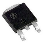
ICGOO电子元器件商城为您提供MAC4DSMT4G由ON Semiconductor设计生产,在icgoo商城现货销售,并且可以通过原厂、代理商等渠道进行代购。 MAC4DSMT4G价格参考。ON SemiconductorMAC4DSMT4G封装/规格:晶闸管 - TRIAC, TRIAC Logic - Sensitive Gate 600V 4A Surface Mount DPAK。您可以下载MAC4DSMT4G参考资料、Datasheet数据手册功能说明书,资料中有MAC4DSMT4G 详细功能的应用电路图电压和使用方法及教程。
MAC4DSMT4G 是安森美(ON Semiconductor)推出的高可靠性、小封装(SOT-23)双向可控硅(TRIAC),额定通态电流 IT(RMS) 为4A,触发电流 IG(T) 典型值仅5mA,支持零交叉或非零交叉触发,具备良好的dv/dt抗干扰能力(≥10V/μs)和高结温(Tj = 125°C),采用无铅环保封装。

其典型应用场景包括:
1. 智能家电控制:如洗衣机、空调、微波炉中的交流电机调速、加热器通断控制;
2. 固态继电器(SSR)模块:替代机械继电器,用于PLC输出端、工业控制板的交流负载开关;
3. LED/LCD背光调光电路:配合过零检测电路实现相位控制调光(如台灯、商业照明);
4. 小型电源与适配器:用于输入级浪涌抑制、待机电源启停管理;
5. IoT终端设备:在空间受限的智能家居节点(如智能插座、温控器)中实现低功耗、高集成度的AC负载驱动。

SOT-23封装便于自动化贴装与高密度PCB布局,配合简单外围电路(如RC缓冲网络、触发隔离光耦)即可可靠工作,适用于对尺寸、成本及可靠性均有要求的中低功率(≤500W)交流开关应用。
| 参数 | 数值 |
| 产品目录 | |
| 描述 | TRIAC SENS GATE 600V 4A DPAK双向可控硅 THY 4A 600V TRIAC |
| 产品分类 | 双向可控硅分离式半导体 |
| GateTriggerCurrent-Igt | 10 mA |
| GateTriggerVoltage-Vgt | 1.3 V |
| 品牌 | ON Semiconductor |
| 产品手册 | |
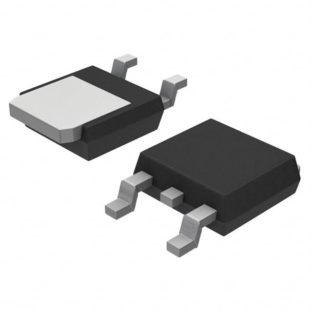
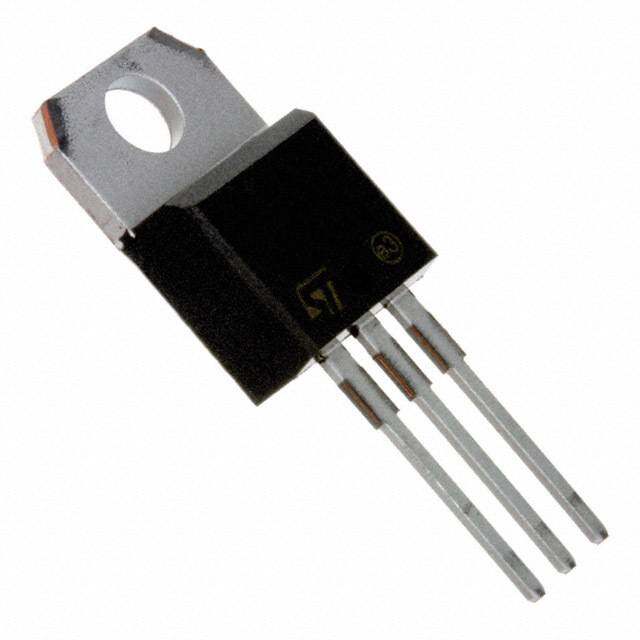
| 产品图片 |
|
| rohs | 符合RoHS无铅 / 符合限制有害物质指令(RoHS)规范要求 |
| 产品系列 | 晶体闸流管,双向可控硅,ON Semiconductor MAC4DSMT4G- |
| 数据手册 | |
| 产品型号 | MAC4DSMT4G |
| PCN组件/产地 | |
| 三端双向可控硅类型 | 逻辑 - 灵敏栅极 |
| 不重复通态电流 | 40 A |
| 产品目录页面 | |
| 产品种类 | 双向可控硅 |
| 供应商器件封装 | DPAK-3 |
| 保持电流Ih最大值 | 15 mA |
| 关闭状态漏泄电流(在VDRMIDRM下) | 0.01 mA |
| 其它名称 | MAC4DSMT4GOSDKR |
| 包装 | Digi-Reel® |
| 商标 | ON Semiconductor |
| 安装类型 | 表面贴装 |
| 安装风格 | SMD/SMT |
| 封装 | Reel |
| 封装/外壳 | TO-252-3,DPak(2 引线+接片),SC-63 |
| 封装/箱体 | DPAK-3 |
| 工厂包装数量 | 2500 |
| 开启状态电压 | 1.6 V |
| 最大工作温度 | + 125 C |
| 最大转折电流IBO | 40 A |
| 最小工作温度 | - 40 C |
| 栅极触发电压-Vgt | 1.3 V |
| 栅极触发电流-Igt | 10 mA |
| 标准包装 | 1 |
| 电压-断态 | 600V |
| 电压-栅极触发(Vgt)(最大值) | 1.3V |
| 电流-不重复浪涌50、60Hz(Itsm) | 40A @ 60Hz |
| 电流-保持(Ih)(最大值) | 15mA |
| 电流-栅极触发(Igt)(最大值) | 10mA |
| 电流-通态(It(RMS))(最大值) | 4A |
| 系列 | MAC4DSM |
| 配置 | 单一 |
| 零件号别名 | MAC4DSM-1G |
| 额定重复关闭状态电压VDRM | 600 V |


- 商务部:美国ITC正式对集成电路等产品启动337调查
- 曝三星4nm工艺存在良率问题 高通将骁龙8 Gen1或转产台积电
- 太阳诱电将投资9.5亿元在常州建新厂生产MLCC 预计2023年完工
- 英特尔发布欧洲新工厂建设计划 深化IDM 2.0 战略
- 台积电先进制程称霸业界 有大客户加持明年业绩稳了
- 达到5530亿美元!SIA预计今年全球半导体销售额将创下新高
- 英特尔拟将自动驾驶子公司Mobileye上市 估值或超500亿美元
- 三星加码芯片和SET,合并消费电子和移动部门,撤换高东真等 CEO
- 三星电子宣布重大人事变动 还合并消费电子和移动部门
- 海关总署:前11个月进口集成电路产品价值2.52万亿元 增长14.8%


PDF Datasheet 数据手册内容提取
Thyristors Surface Mount – 600V - 800V > MAC4DSM, MAC4DSN MAC4DSM, MAC4DSN Pb Description Designed for high volume, low cost, industrial and consumer applications such as motor control; process control; temperature, light and speed control. Features • Small Size Surface Mount DPAK Package • Passivated Die for Reliability and Uniformity • Blocking Voltage to 800 V • On−State Current Rating of 4.0 A RMS at 108°C • Low IGT − 10 mA Maximum in 3 Quadrants • High Immunity to dv/dt − 50 V/μs at 125°C • Epoxy Meets UL 94 V−0 @ 0.125 in Pin Out • ESD Ratings: Human Body Model, 3B > 8000 V Machine Model, C > 400 V • Pb−Free Packages are Available 4 4 1 2 Functional Diagram 3 1 2 MT2 MT1 G Additional Information Datasheet Resources Samples © 2017 Littelfuse, Inc. Specifications are subject to change without notice. Revised: 08/30/17
Thyristors Surface Mount – 600V - 800V > MAC4DSM, MAC4DSN Maximum Ratings (T = 25°C unless otherwise noted) J Rating Symbol Value Unit Peak Repetitive Off-State Voltage (Note 1) V , DRM (Gate Open, Sine Wave 50 to 60 Hz, T = -40° to 110°C) J MAC4DSM VRRM 600 V MAC4DSN 800 On-State RMS Current (Full Cycle Sine Wave, 60 Hz, T = 108°C) I 4.0 A C T (RMS) Peak Non-Repetitive Surge Current I 40 A (One Full Cycle Sine Wave, 60 Hz, T = 108°C) TSM C Circuit Fusing Consideration (t = 8.3 msec) I2t 6.6 A²sec Peak Gate Current (Pulse Width ≤ 20 µsec, T = 108°C) I 4.0 W C GM Peak Gate Power (Pulse Width ≤ 10 µsec, T = 108°C) P 2.0 W C GM Peak Gate Voltage (Pulse Width ≤ 20 µsec, T = 108°C) V 5.0 V C GM Average Gate Power (t = 8.3 msec, T = 108°C) P 1.0 W C G(AV) Operating Junction Temperature Range T -40 to +125 °C J Storage Temperature Range T -40 to +150 °C stg Stresses exceeding Maximum Ratings may damage the device. Maximum Ratings are stress ratings only. Functional operation above the Recommended Operating Conditions is not implied. Extended exposure to stresses above the Recommended Operating Conditions may affect device reliability. 1. V and V for all types can be applied on a continuous basis. Ratings apply for zero or negative gate voltage; however, positive gate voltage shall not be applied concurrent with negative DRM RRM potential on the anode. Blocking voltages shall not be tested with a constant current source such that the voltage ratings of the devices are exceeded. Thermal Characteristics Rating Symbol Value Unit R Thermal Resistance, Junction−to−Case (AC) 8JC 3.5 Junction−to−Ambient R 88 °C/W 8JA Junction−to−Ambient (Note 2) R 80 8JA Maximum Lead Temperature for Soldering Purposes, 1/8” from case for T 260 °C 10 seconds (Note 3) L 2. These ratings are applicable when surface mounted on the minimum pad sizes recommended. 3. 1/8" from case for 10 seconds. © 2017 Littelfuse, Inc. Specifications are subject to change without notice. Revised: 08/30/17
Thyristors Surface Mount – 600V - 800V > MAC4DSM, MAC4DSN Electrical Characteristics - OFF (T = 25°C unless otherwise noted ; Electricals apply in both directions) J Characteristic Symbol Min Typ Max Unit Peak Repetitive Blocking Current TJ = 25°C I , - - 0.01 (V = V = V ; Gate Open) DRM mA D D R M R R M T = 125°C IRRM - - 2.0 J Electrical Characteristics - ON (T = 25°C unless otherwise noted; Electricals apply in both directions) J Characteristic Symbol Min Typ Max Unit Peak On−State Voltage (Note 4) (I = ±6.0 A) V − 1.3 1.6 V TM TM MT2(+), G(+) 2.9 4.0 10 Gate Trigger Current MT2(+), G(−) I 2.9 5.0 10 mA (Continuous dc) GT (V = 12 V, R = 100 Ω) D L MT2(−), G(−) 2.9 7.0 10 Holding Current (V = 12 V, Gate Open, Initiating Current = ±200 mA)) I 0.2 5.5 1.5 mA D H MT2(+), G(+) _ 6.0 30 Latching Current MT2(+), G(−) I _ 10 30 mA L MT2(−), G(−) _ 6.0 30 MT2(+), G(+) 0.5 0.7 1.3 Gate Trigger Voltage (Continuous dc) MT2(+), G(−) V 0.5 0.65 1.3 V GT (V = 12 V, R = 100 Ω) D L MT2(−), G(−) 0.5 0.7 1.3 MT2(+), G(+) 0.2 0.4 − Gate Non−Trigger Voltage (T = 125°C) MT2(+), G(−) V 0.2 0.4 − V J GD (V = 12 V, R = 100 Ω) D L MT2(−), G(−) 0.2 0.4 − 4. Indicates Pulse Test: Pulse Width ≤ 2.0 ms, Duty Cycle ≤ 2%. © 2017 Littelfuse, Inc. Specifications are subject to change without notice. Revised: 08/30/17
Thyristors Surface Mount – 600V - 800V > MAC4DSM, MAC4DSN Dynamic Characteristics Characteristic Symbol Min Typ Max Unit Rate of Change of Commutating Current (V = 400 V, I = 3.5 A, Commutating dv/dt = 10 V/µsec, Gate Open, D TM (dI/dt)c 3.0 4.0 − A/ms T = 125°C, f = 500 Hz, CL = 5.0 µF, LL = 20 mH, No Snubber) See Figure 16 J Critical Rate of Rise of Off-State Voltage dV/dt 50 175 − V/µs (V = 0.67 x V , Exponential Waveform, Gate Open, T = 125°C) D DRM J Voltage Current Characteristic of SCR Symbol Parameter +Current V Peak Repetitive Forward Off State Voltage Quadrant 1 DRM MainTerminal 2 + VTM I Peak Forward Blocking Current DRM on state IH V Peak Repetitive Reverse Off State Voltage IRRM at VRRM RRM I Peak Reverse Blocking Current off state +Voltage RRM IH IDRM at VDRM V Maximum On State Voltage Quadrant 3 TM MainTerminal 2 VTM I Holding Current H Quadrant Definitions for a Triac MT2 POSITIVE (Positive Half Cycle) + (+) MT2 (+) MT2 QuadrantII ( ) IGT (+) IGT QuadrantI GATE GATE MT1 MT1 REF REF IGT +IGT ( ) MT2 ( ) MT2 QuadrantIII ( ) IGT (+) IGT QuadrantIV GATE GATE MT1 MT1 REF REF MT2 NEGATIVE (Negative Half Cycle) All polarities are referenced to MT1. With inphase signals (using standard AC lines) quadrants I and III are used. © 2017 Littelfuse, Inc. Specifications are subject to change without notice. Revised: 08/30/17
Thyristors Surface Mount – 600V - 800V > MAC4DSM, MAC4DSN Figure 1. Typical RMS Current Derating Figure 2. On-State Power Dissipation Figure 3. On−State Characteristics Figure 4. Transient Thermal Response MPS)100 ED) 1.0 E CURRENT (A 10 TYPICAL @ TJ = 25°C MAXIMUM @ JT = 125°C CE (NORMALIZ US ON-STAT MAXIMUM @ JT = 25°C T RESISTAN 0.1 Z JC(t) = R JC(t)r(t) O 1.0 N E E I, INSTANTANT0.10 1.0 2.0 3.0 4.0 5.0 r, TRANSI(t) 0.01 0.1 1.0 10 100 1000 10 K t, TIME (ms) VT, INSTANTANEOUS ON-STATE VOLTAGE (VOLTS) Figure 5. Typical Gate Trigger Current vs, Junction Temperature Figure 6. Typical Gate Trigger Voltage vs. Junction Temperature © 2017 Littelfuse, Inc. Specifications are subject to change without notice. Revised: 08/30/17
Thyristors Surface Mount – 600V - 800V > MAC4DSM, MAC4DSN Figure 7. Typical Holding Current vs. Junction Temperature Figure 8. Typical Latching Current vs.Junction Temperature 14 25 Q2 12 A) A) 20 m m T ( 10 T ( N MT2 NEGATIVE N Q1 E E RR 8.0 RR 15 CU CU Q3 DING 6.0 MT2 POSITIVE HING 10 L C HO 4.0 AT I, H , LIL5.0 2.0 0 0 -50 -25 0 25 50 75 100 125 -50 -25 0 25 50 75 100 125 TJ, JUNCTION TEMPERATURE (°C) TJ, JUNCTION TEMPERATURE (°C) Figure 9. Exponential Static dv/dt vs. Figure 10. Exponential Static dv/dt vs. Gate−MT1 Resistance, MT2(+) Gate−MT1 Resistance, MT2(-) 1000 1200 TJ = 125°C TJ = 125°C 1000 VPK = 400 V 800 STATIC dv/dt (V/ s) 640000 600 V VPK = 400 V STATIC dv/dt (V/ s) 864000000 600 V 200 800 V 200 800 V 0 0 100 1000 10 k 100 1000 10 k RG-MT1, GATE-MT1 RESISTANCE (OHMS) RG-MT1, GATE-MT1 RESISTANCE (OHMS) Figure 9. Exponential Static dv/dt vs. Figure 10. Exponential Static dv/dt vs. Gate−MT1 Resistance, MT2(+) Gate−MT1 Resistance, MT2(-) 800 2000 GATE OPEN 1600 GATE OPEN C dv/dt (V/ s) 640000 110°C TJ = 100°C C dv/dt (V/ s)1200 TJ = 100°C 110°C STATI 125°C STATI 800 125°C 200 400 0 0 400 500 600 700 800 400 500 600 700 800 VPK, PEAK VOLTAGE (VOLTS) VPK, PEAK VOLTAGE (VOLTS) © 2017 Littelfuse, Inc. Specifications are subject to change without notice. Revised: 08/30/17
Thyristors Surface Mount – 600V - 800V > MAC4DSM, MAC4DSN Figure 13. Typical Holding Current vs. Junction Temperature Figure 14. Typical Latching Current vs.Junction Temperature 800 1600 GATE OPEN 1400 GATE OPEN 600 VPK = 400 V 1200 VPK = 400 V V/ s) V/ s) 1000 dt ( dt ( C dv/ 400 600 V C dv/ 800 600 V ATI ATI 600 T T S S 200 400 800 V 200 800 V 0 0 100 105 110 115 120 125 100 105 110 115 120 125 TJ, JUNCTION TEMPERATURE °(C) TJ, JUNCTION TEMPERATURE °(C) Figure 15. Typical Holding Current vs. Junction Temperature 100 VPK = 400 V OFs) ATE OF RISE OLTAGE (V/ TJ = 125°C 100°C 75°C dv/dt(c), CRITICAL RCOMMUTATING V 10 VDRMtw f (=di/2d1 ttw)c =61f0 I0T0M 1.0 0 5.0 10 15 20 di/dt(c), RATE OF CHANGE OF COMMUTATING CURRENT (A/ms) Figure 16. Simplified Test Circuit to Measure the Critical Rate of Rise of Commutating Current (di/dt) LL 1N4007 200 VRMS ADJUST FOR MEASURE TM, 60 Hz VAC I CHARGE L CHARGE TRIGGER CONTROL TRO - 200 V ON + R C MT2 GGE 1N91451 RI MT1 T G CL Note: Component values are for verification of rated (di/dt)c. See AN1048 for additional information. © 2017 Littelfuse, Inc. Specifications are subject to change without notice. Revised: 08/30/17
Thyristors Surface Mount – 600V - 800V > MAC4DSM, MAC4DSN Dimensions Soldering Footprint DPAK CASE 369C 6.20 3.0 ISSUE O 0.244 0.118 2.58 T SEATING PLANE 0.101 B C V R E 5.80 1.6 6.172 0.228 0.063 0.243 4 Z A S 12 3 U mm K SCALE 3:1 inches F J L H D2 PL G 0.13 (0.005) M T Inches Millimeters Dim Min Max Min Max A 0.235 0.245 5.97 6.35 B 0.250 0.265 6.35 6.73 C 0.086 0.094 2.19 2.38 D 0.027 0.035 0.69 0.88 E 0.018 0.023 0.46 0.58 F 0.037 0.045 0.94 1.14 G 0.090 BSC 2.29 BSC H 0.034 0.040 0.87 1.01 J 0.018 0.023 0.46 0.58 K 0.350 0.380 8.89 9.65 R 0.180 0.215 4.45 5.45 S 0.025 0.040 0.63 1.01 V 0.035 0.050 0.89 1.27 Z 0.155 −−− 3.93 −−− 1. DIMENSIONING AND TOLERANCING PER ANSI Y14.5M, 1982. 2. CONTROLLING DIMENSION: INCH. STYLE 6: PIN 1. MT1 2. MT2 3. GATE 4. MT2 © 2017 Littelfuse, Inc. Specifications are subject to change without notice. Revised: 08/30/17
Thyristors Surface Mount – 600V - 800V > MAC4DSM, MAC4DSN Dimensions Part Marking System DPAK 3 4 01 DPAK CASE 369C YWW 1 2 STYLE 6 AC 3 4DSxG B C V R E 4 4 DPAK 3 YWW Z A CASE 369D AC S 4DSxG 12 3 STYLE 6 1 T 2 3 SEATING PLANE K Y= Year WW = Work Week F J AC4DCx = Device Code H x= M or N D3 PL G= Pb Free Package G 0.13 (0.005) M T Pin Assignment Inches Millimeters Dim 1 Main Terminal 1 Min Max Min Max 2 Main Terminal 2 A 0.235 0.245 5.97 6.35 B 0.250 0.265 6.35 6.73 3 Gate C 0.086 0.094 2.19 2.38 4 Main Terminal 2 D 0.027 0.035 0.69 0.88 E 0.018 0.023 0.46 0.58 Ordering Information F 0.037 0.045 0.94 1.14 G 0.090 BSC 2.29 BSC Package Device Package Shipping H 0.034 0.040 0.87 1.01 Type J 0.018 0.023 0.46 0.58 MAC4DSM−001 DPAK−3 369D 75 Units / Rail K 0.350 0.380 8.89 9.65 R 0.180 0.215 4.45 5.45 DPAK−3 MAC4DSM−001G 369D 75 Units / Rail (Pb−Free) S 0.025 0.040 0.63 1.01 V 0.035 0.050 0.89 1.27 2500 / Tape & MAC4DSMT4 DPAK−3 369C Reel Z 0.155 −−− 3.93 −−− DPAK−3 2500 / Tape & 1. DIMENSIONING AND TOLERANCING PER ANSI Y14.5M, MAC4DSMT4G (Pb−Free) 369C Reel 1982. 2. CONTROLLING DIMENSION: INCH. MAC4DSN−001 DPAK−3 369D 75 Units / Rail STYLE 6: PIN 1. MT1 DPAK−3 MAC4DSN−001G 369D 75 Units / Rail 2. MT2 (Pb−Free) 3. GATE 4. MT2 MAC4DSNT4 DPAK−3 369C 2500 / Tape & Reel Disclaimer Notice - Information furnished is believed to be accurate and reliable. However, users should independently evaluate the suitability of and test each product selected for their own applications. Littelfuse products are not designed for, and may not be used in, all applications. Read complete Disclaimer Notice at: www.littelfuse.com/disclaimer-electronics © 2017 Littelfuse, Inc. Specifications are subject to change without notice. Revised: 08/30/17