ICGOO在线商城 > 分立半导体产品 > 晶闸管 - TRIAC > BTA12-600BW3G
 Datasheet下载
- 型号: BTA12-600BW3G
- 制造商: ON Semiconductor
- 库位|库存: xxxx|xxxx
- 要求:
| 数量阶梯 | 香港交货 | 国内含税 |
| +xxxx | $xxxx | ¥xxxx |
查看当月历史价格
查看今年历史价格
BTA12-600BW3G产品简介:
ICGOO电子元器件商城为您提供BTA12-600BW3G由ON Semiconductor设计生产,在icgoo商城现货销售,并且可以通过原厂、代理商等渠道进行代购。 BTA12-600BW3G价格参考¥6.18-¥7.20。ON SemiconductorBTA12-600BW3G封装/规格:晶闸管 - TRIAC, TRIAC Standard 600V 12A Through Hole TO-220AB。您可以下载BTA12-600BW3G参考资料、Datasheet数据手册功能说明书,资料中有BTA12-600BW3G 详细功能的应用电路图电压和使用方法及教程。
Littelfuse Inc.生产的BTA12-600BW3G是一种双向晶闸管(TRIAC),广泛应用于交流电力控制领域。以下是该型号的主要应用场景:

 1. 家用电器
   BTA12-600BW3G常用于家用电器的调光和调速控制,如:
   - 调光灯具:通过调节交流电压的导通角来控制灯光亮度,适用于LED灯、白炽灯等。
   - 风扇调速:用于控制风扇的速度,提供不同的风力档位选择。
   - 电暖器:调节加热功率,以适应不同的温度需求。

 2. 工业自动化
   在工业环境中,BTA12-600BW3G可以用于电机控制、加热元件的功率调节等场景:
   - 电机软启动:通过逐步增加电流,减少电机启动时的冲击电流,延长设备寿命。
   - 加热控制:在电炉、热处理设备中,精确控制加热元件的功率输出,确保温度稳定。

 3. 智能控制系统
   随着智能家居和物联网的发展,BTA12-600BW3G也广泛应用于智能控制系统中:
   - 智能插座:通过Wi-Fi或蓝牙控制电源开关,实现远程控制家电设备的开闭。
   - 智能照明系统:与传感器结合,自动调节灯光亮度或开关状态,提升能源利用效率。

 4. 电动工具
   在电动工具中,BTA12-600BW3G可用于调节工具的工作速度或功率:
   - 电钻、砂轮机:根据实际需要调整工作速度,提高工作效率和安全性。

 5. 舞台灯光控制
   在娱乐行业,尤其是舞台灯光系统中,BTA12-600BW3G用于控制灯光效果:
   - 灯光渐变:实现灯光从暗到亮或从亮到暗的平滑过渡,营造不同的舞台氛围。
   - 频闪效果:通过快速开关控制,产生频闪效果,增强视觉冲击力。

 总结
BTA12-600BW3G作为一种高性能的双向晶闸管,凭借其高耐压、大电流承载能力和可靠的开关特性,广泛应用于家用电器、工业自动化、智能控制系统、电动工具以及舞台灯光等领域,能够有效实现对交流电力的精确控制。
| 参数 | 数值 |
| 产品目录 | |
| 描述 | TRIAC 600V 12A TO220AB双向可控硅 12A 50mA 600V IGT 3 QUAD INTERNL ISLTD |
| 产品分类 | 双向可控硅分离式半导体 |
| GateTriggerCurrent-Igt | 50 mA |
| GateTriggerVoltage-Vgt | 1.7 V |
| 品牌 | ON Semiconductor |
| 产品手册 | |
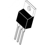
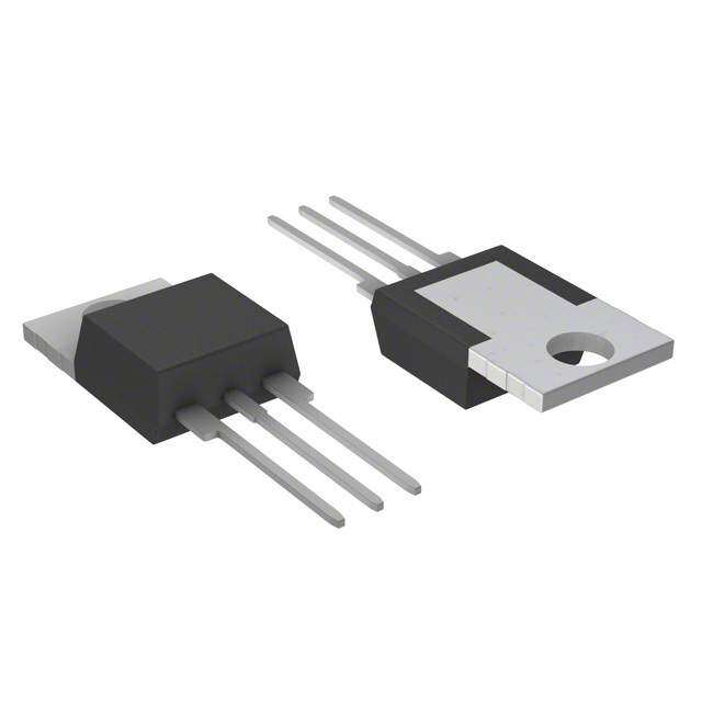
| 产品图片 |
|
| rohs | 符合RoHS无铅 / 符合限制有害物质指令(RoHS)规范要求 |
| 产品系列 | 晶体闸流管,双向可控硅,ON Semiconductor BTA12-600BW3G- |
| 数据手册 | |
| 产品型号 | BTA12-600BW3G |
| 三端双向可控硅类型 | 标准 |
| 不重复通态电流 | 105 A |
| 产品种类 | 双向可控硅 |
| 供应商器件封装 | TO-220AB |
| 保持电流Ih最大值 | 50 mA |
| 关闭状态漏泄电流(在VDRMIDRM下) | 0.005 mA |
| 其它名称 | BTA12-600BW3G-ND |
| 包装 | 管件 |
| 商标 | ON Semiconductor |
| 安装类型 | 通孔 |
| 安装风格 | Through Hole |
| 封装/外壳 | TO-220-3 |
| 封装/箱体 | TO-220-3 |
| 工厂包装数量 | 50 |
| 开启状态电压 | 1.55 V |
| 最大工作温度 | + 125 C |
| 最小工作温度 | - 40 C |
| 栅极触发电压-Vgt | 1.7 V |
| 栅极触发电流-Igt | 50 mA |
| 标准包装 | 50 |
| 电压-断态 | 600V |
| 电压-栅极触发(Vgt)(最大值) | 1.1V |
| 电流-不重复浪涌50、60Hz(Itsm) | 105A @ 60Hz |
| 电流-保持(Ih)(最大值) | 50mA |
| 电流-栅极触发(Igt)(最大值) | 50mA |
| 电流-通态(It(RMS))(最大值) | 12A |
| 系列 | BTA12-50MA |
| 配置 | 单一 |
| 额定重复关闭状态电压VDRM | 600 V |


- 商务部:美国ITC正式对集成电路等产品启动337调查
- 曝三星4nm工艺存在良率问题 高通将骁龙8 Gen1或转产台积电
- 太阳诱电将投资9.5亿元在常州建新厂生产MLCC 预计2023年完工
- 英特尔发布欧洲新工厂建设计划 深化IDM 2.0 战略
- 台积电先进制程称霸业界 有大客户加持明年业绩稳了
- 达到5530亿美元!SIA预计今年全球半导体销售额将创下新高
- 英特尔拟将自动驾驶子公司Mobileye上市 估值或超500亿美元
- 三星加码芯片和SET,合并消费电子和移动部门,撤换高东真等 CEO
- 三星电子宣布重大人事变动 还合并消费电子和移动部门
- 海关总署:前11个月进口集成电路产品价值2.52万亿元 增长14.8%


PDF Datasheet 数据手册内容提取
Thyristors Surface Mount – 800V > BTA12-600BW3G, BTA12-800BW3G, BTA12-600BW3G, BTA12-800BW3G, Pb Description Designed for high performance full−wave ac control applications where high noise immunity and high commutating di/dt are required. Features • Blocking Voltage to 800 V • On-State Current Rating of 12 A RMS at 25°C • Uniform Gate Trigger Currents in Three Quadrants • High Immunity to dV/dt − 2000 V/µs minimum at 125°C • Minimizes Snubber Networks for Protection • Industry Standard TO-220AB Package • High Commutating dI/dt − 2.5 A/ms minimum at 125°C Pin Out • Internally Isolated (2500 VRMS) • These Devices are Pb−Free and are RoHS Compliant Functional Diagram MT2 MT1 G CASE 221A STYLE 4 1 2 Additional Information Datasheet Resources Samples © 2017 Littelfuse, Inc. Specifications are subject to change without notice. Revised: 08/30/17
Thyristors Surface Mount – 800V > BTA12-600BW3G, BTA12-800BW3G, Maximum Ratings (T = 25°C unless otherwise noted) J Rating Symbol Value Unit Peak Repetitive Off-State Voltage (Note 1) V , (Gate Open, Sine Wave 50 to 60 Hz, T = -40° to 125°C) DRM J V V BTA12−600BW3G RRM 600 BTA12−800BW3G 800 On-State RMS Current (Full Cycle Sine Wave, 60 Hz, T = 80°C) I 12 A C T (RMS) Peak Non-Repetitive Surge Current I 105 A (One Full Cycle Sine Wave, 60 Hz, T = 25°C) TSM C Circuit Fusing Consideration (t = 8.3 ms) I2t 46 A²sec Non−Repetitive Surge Peak Off−State Voltage (T = 25°C, t = 10ms) V / V V / V V J DSM RSM DSM RSM +100 Peak Gate Current (T = 125°C, t = 20ms) I 4.0 A J GM Peak Gate Power (Pulse Width ≤ 1.0 µs, TC = 80°C) PG(AV) 20 W Average Gate Power (T = 125°C) P 1.0 W J G(AV) Operating Junction Temperature Range T -40 to +125 °C J Storage Temperature Range T -40 to +125 °C stg RMS Isolation Voltage (t = 300 ms, R.H.≤ 30%, T = 25°C) V 2500 V A iso Stresses exceeding Maximum Ratings may damage the device. Maximum Ratings are stress ratings only. Functional operation above the Recommended Operating Conditions is not implied. Extended exposure to stresses above the Recommended Operating Conditions may affect device reliability. 1. V and V for all types can be applied on a continuous basis. Ratings apply for zero or negative gate voltage; however, positive gate voltage shall not be applied concurrent with negative DRM RRM potential on the anode. Blocking voltages shall not be tested with a constant current source such that the voltage ratings of the devices are exceeded. Thermal Characteristics Rating Symbol Value Unit Thermal Resistance, Junction−to−Case (AC) R 2.5 8JC °C/W Junction−to−Ambient R 60 8JA Maximum Lead Temperature for Soldering Purposes, 1/8” from case for T 260 °C 10 seconds L © 2017 Littelfuse, Inc. Specifications are subject to change without notice. Revised: 08/30/17
Thyristors Surface Mount – 800V > BTA12-600BW3G, BTA12-800BW3G, Electrical Characteristics - OFF (T = 25°C unless otherwise noted ; Electricals apply in both directions) J Characteristic Symbol Min Typ Max Unit Peak Repetitive Blocking Current TJ = 25°C I , - - 0.005 (V = V = V ; Gate Open) DRM mA D D R M R R M T = 125°C IRRM - - 2.0 J Electrical Characteristics - ON (T = 25°C unless otherwise noted; Electricals apply in both directions) J Characteristic Symbol Min Typ Max Unit Forward On-State Voltage (Note 2) (I = ±17 A Peak) V − − 1.55 V TM TM MT2(+), G(+) 2.5 − 50 Gate Trigger Current (Continuous dc) (V = 12 V, R = 30 Ω) D L MT2(+), G(−) I 2.5 − 50 mA GT MT2(−), G(−) 2.5 − 50 Holding Current IH − − 50 mA (V = 12 V, Gate Open, Initiating Current = ±100 mA) D MT2(+), G(+) − − 70 Latching Current (V = 24 V, I = 60 mA) MT2(+), G(−) IL − − 80 mA D G MT2(−), G(−) − − 70 MT2(+), G(+) 0.5 − 1.7 Gate Trigger Voltage (V = 12 V, R = 30 Ω) MT2(+), G(−) V 0.5 − 1.1 V D L GT MT2(−), G(−) 0.5 − 1.1 MT2(+), G(+) 0.2 − − Gate Non−Trigger Voltage (T = 125°C) MT2(+), G(−) t 0.2 − − V J gt MT2(−), G(−) 0.2 − − 2. Indicates Pulse Test: Pulse Width ≤ 2.0 ms, Duty Cycle ≤ 2%. © 2017 Littelfuse, Inc. Specifications are subject to change without notice. Revised: 08/30/17
Thyristors Surface Mount – 800V > BTA12-600BW3G, BTA12-800BW3G, Dynamic Characteristics Characteristic Symbol Min Typ Max Unit Rate of Change of Commutating Current, See Figure 10. (dI/dt)c 2.5 − − A/ms (Gate Open, T = 125°C, No Snubber) J Critical Rate of Rise of On−State Current dI/dt − − 50 A/µs (T = 125°C, f = 120 Hz, I = 2 x I , tr ≤ 100 ns) J G GT Critical Rate of Rise of Off-State Voltage (V = 0.66 x V , Exponential Waveform, Gate Open, T = 125°C) dV/dt 2000 − − V/µs D DRM J Voltage Current Characteristic of SCR Symbol Parameter +Current V Peak Repetitive Forward Off State Voltage Quadrant 1 DRM MainTerminal 2 + VTM I Peak Forward Blocking Current DRM on state IH V Peak Repetitive Reverse Off State Voltage IRRM at VRRM RRM I Peak Reverse Blocking Current off state +Voltage RRM IH IDRM at VDRM V Maximum On State Voltage Quadrant 3 TM MainTerminal 2 VTM I Holding Current H Quadrant Definitions for a Triac MT2 POSITIVE (Positive Half Cycle) + (+) MT2 (+) MT2 QuadrantII ( ) IGT (+) IGT QuadrantI GATE GATE MT1 MT1 REF REF IGT +IGT ( ) MT2 ( ) MT2 QuadrantIII ( ) IGT (+) IGT QuadrantIV GATE GATE MT1 MT1 REF REF MT2 NEGATIVE (Negative Half Cycle) All polarities are referenced to MT1. With inphase signals (using standard AC lines) quadrants I and III are used. © 2017 Littelfuse, Inc. Specifications are subject to change without notice. Revised: 08/30/17
Thyristors Surface Mount – 800V > BTA12-600BW3G, BTA12-800BW3G, Figure 1. RMS Current Derating Figure 2. On-State Power Dissipation 20 125 DC 18 C) W) 16 180° °E (110 120°, 90°, 60°, 30° ER ( 14 120° R W TU O 12 A P R E 10 E G MP 95 RA 8 90° E E ASE T 80 180° , AVAV 64 30°60° C P , C DC 2 T 0 65 0 2 4 6 8 10 12 0 2 4 6 8 10 12 IT(RMS), ON-STATE CURRENT (A) Figure 3. On−State Characteristics Figure 4. Thermal Response D) E Z ALI 1 M R O N ( E C N A T S SI E L R 0.1 A M R E H T T N E SI N A r(t), TR0.010.1 1 10t, TIME (m1s0)0 1000 1·104 Figure 5. Hold Current Variation © 2017 Littelfuse, Inc. Specifications are subject to change without notice. Revised: 08/30/17
Thyristors Surface Mount – 800V > BTA12-600BW3G, BTA12-800BW3G, Figure 6. Gate Trigger Current Variation Figure 7. Gate Trigger Voltage Variation Figure 8. Critical Rate of Rise of Off-State Voltage Figure 10. Latching Current Variation (Exponential Waveform) µ 5000 VD = 800 Vpk 4K TJ = 125°C 3K 2K 1K 0 10 100 1000 10000 RG, GATE TO MAIN TERMINAL 1 RESISTANCE (OHMS) Figure 9. Simplified Test Circuit to Measure the Critical Rate of Rise of Commutating Current (di/dt) Note: Component values are for verification of rated (di/dt)c. See AN1048 for additional information © 2017 Littelfuse, Inc. Specifications are subject to change without notice. Revised: 08/30/17
Thyristors Surface Mount – 800V > BTA12-600BW3G, BTA12-800BW3G, Dimensions Part Marking System 4 SEATING PLANE B F C T S 4 Q A BTA12 xBWG TO 220AB AYWW 12 3 U 1 CASE 221A 2 H 3 STYLE 12 K Z L R x= 6 or 8 V J A= Assembly Location (Optional)* Y= Year G WW = Work Week D G= Pb Free Package N *The Assembly Location code (A) is optional. In cases where the Assembly Location is stamped on the package the assembly code may be blank. Inches Millimeters Pin Assignment Dim Min Max Min Max 1 Main Terminal 1 A 0.570 0.620 14.48 15.75 2 Main Terminal 2 B 0.380 0.405 9.66 10.28 C 0.160 0.190 4.07 4.82 3 Gate D 0.025 0.035 0.64 0.88 4 No Connection F 0.142 0.147 3.61 3.73 G 0.095 0.105 2.42 2.66 H 0.110 0.155 2.80 3.93 Ordering Information J 0.014 0.022 0.36 0.55 K 0.500 0.562 12.70 14.27 Device Package Shipping L 0.045 0.060 1.15 1.52 TO−220AB BTA12−600BW3G 50 Units / Rail N 0.190 0.210 4.83 5.33 (Pb−Free) Q 0.100 0.120 2.54 3.04 TO−220AB BTA12−800BW3G 50 Units / Rail R 0.080 0.110 2.04 2.79 (Pb−Free) S 0.045 0.055 1.15 1.39 T 0.235 0.255 5.97 6.47 U 0.000 0.050 0.00 1.27 V 0.045 −−− 1.15 −−− Z −−− 0.080 −−− 2.04 1. DIMENSIONING AND TOLERANCING PER ANSI Y14.5M, 1982. 2. CONTROLLING DIMENSION: INCH. 3. DIMENSION Z DEFINES A ZONE WHERE ALL BODY AND LEAD IRREGULARITIES ARE ALLOWED. Disclaimer Notice - Information furnished is believed to be accurate and reliable. However, users should independently evaluate the suitability of and test each product selected for their own applications. Littelfuse products are not designed for, and may not be used in, all applications. Read complete Disclaimer Notice at: www.littelfuse.com/disclaimer-electronics. © 2017 Littelfuse, Inc. Specifications are subject to change without notice. Revised: 08/30/17