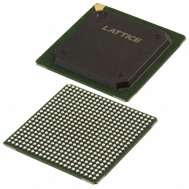
ICGOO在线商城 > 集成电路(IC) > 嵌入式 - CPLD(复杂可编程逻辑器件) > M4A5-64/32-10JNC

 Datasheet下载
- 型号: M4A5-64/32-10JNC
- 制造商: Lattice
- 库位|库存: xxxx|xxxx
- 要求:
| 数量阶梯 | 香港交货 | 国内含税 |
| +xxxx | $xxxx | ¥xxxx |
查看当月历史价格
查看今年历史价格
M4A5-64/32-10JNC产品简介:
ICGOO电子元器件商城为您提供M4A5-64/32-10JNC由Lattice设计生产,在icgoo商城现货销售,并且可以通过原厂、代理商等渠道进行代购。 M4A5-64/32-10JNC价格参考。LatticeM4A5-64/32-10JNC封装/规格:嵌入式 - CPLD(复杂可编程逻辑器件), 。您可以下载M4A5-64/32-10JNC参考资料、Datasheet数据手册功能说明书,资料中有M4A5-64/32-10JNC 详细功能的应用电路图电压和使用方法及教程。
Lattice Semiconductor Corporation(莱迪思半导体公司)的M4A5-64/32-10JNC是一款嵌入式CPLD(复杂可编程逻辑器件),属于ispMACH 4000A系列。这类器件主要应用于需要灵活逻辑控制、信号调理和接口桥接的场景,以下是其典型应用场景:

 1. 工业自动化
   - 设备控制:用于实现工业设备中的状态机控制、传感器数据采集和驱动器接口。
   - 实时信号处理:处理来自传感器或执行器的高速信号,提供快速响应。
   - 协议转换:在不同通信协议之间进行桥接,例如将RS-232信号转换为SPI或I2C。

 2. 通信设备
   - 接口扩展:为通信模块增加GPIO、UART或其他接口,满足多样化的连接需求。
   - 信号调理:对输入输出信号进行电平转换或滤波处理。
   - 时钟管理:生成或分配系统所需的时钟信号,确保同步操作。

 3. 消费电子
   - 嵌入式控制器:在小型家电或消费类电子产品中用作主控芯片的辅助逻辑单元。
   - 显示驱动:支持LCD或LED显示屏的驱动和刷新控制。
   - 电源管理:监控和控制电源状态,实现低功耗模式切换。

 4. 汽车电子
   - 车载信息娱乐系统:用于音频视频信号的切换和处理。
   - 传感器融合:整合多个传感器的数据,优化车辆控制系统性能。
   - 安全功能:实现紧急制动、碰撞检测等逻辑控制。

 5. 医疗设备
   - 仪器控制:管理医疗设备中的数据采集和处理流程。
   - 患者监测:处理来自心率、血压等传感器的信号,并传输至主处理器。
   - 用户界面:控制按钮、触摸屏或指示灯的交互逻辑。

 6. 军事与航空航天
   - 高可靠性应用:由于其低功耗和高可靠性特点,适用于恶劣环境下的任务关键型设备。
   - 信号路由:在复杂的通信或导航系统中实现信号的动态路由。

 核心优势
- 低功耗:适合对功耗敏感的应用场景。
- 小封装:易于集成到空间受限的设计中。
- 即时编程:支持现场可编程特性,便于快速开发和调试。
- 高性价比:相比FPGA,更适合中小型逻辑设计。

综上,M4A5-64/32-10JNC CPLD广泛应用于需要高效逻辑控制、信号处理和接口扩展的领域,尤其适合资源有限但功能需求多样的嵌入式系统。
| 参数 | 数值 |
| 产品目录 | 集成电路 (IC)半导体 |
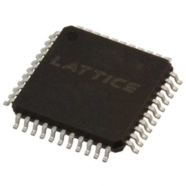
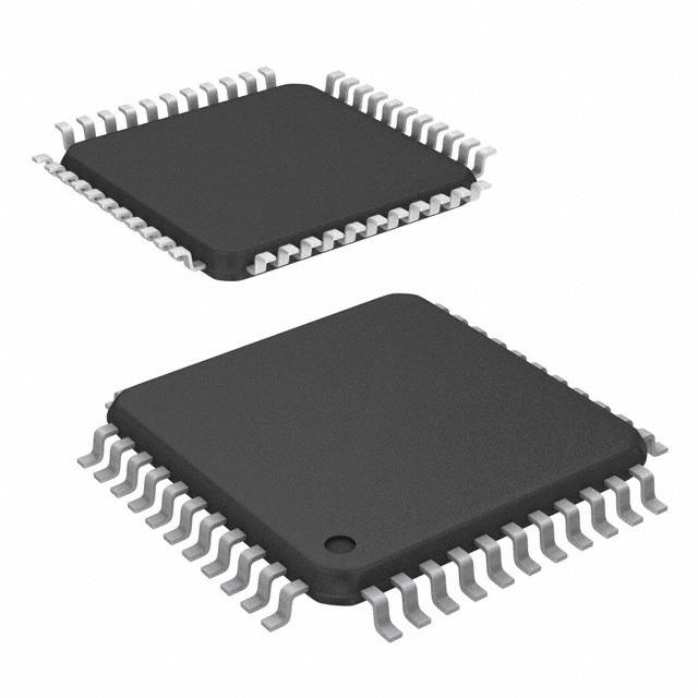
| 描述 | IC CPLD 64MC 10NS 44PLCCCPLD - 复杂可编程逻辑器件 64 MC 32 IO JTAG ISP 5V 10ns |
| 产品分类 | |
| I/O数 | 32 |
| 品牌 | Lattice Semiconductor Corporation |
| 产品手册 | |
| 产品图片 |
|
| rohs | 符合RoHS无铅 / 符合限制有害物质指令(RoHS)规范要求 |
| 产品系列 | 嵌入式处理器和控制器,CPLD - 复杂可编程逻辑器件,Lattice M4A5-64/32-10JNCispMACH® 4A |
| 数据手册 | |
| 产品型号 | M4A5-64/32-10JNC |
| 产品 | ispMACH 4A |
| 产品种类 | CPLD - 复杂可编程逻辑器件 |
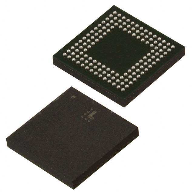
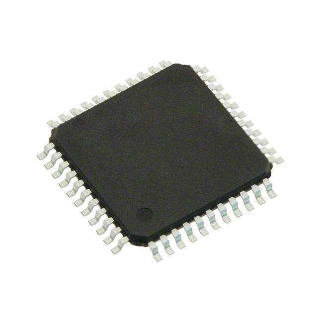
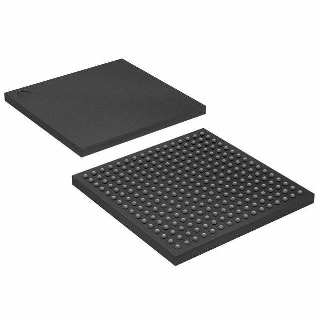
| 供应商器件封装 | 44-PLCC(16.58x16.58) |
| 其它名称 | 220-1845 |
| 包装 | 管件 |
| 可编程类型 | 系统内可编程 |
| 商标 | Lattice |
| 大电池数量 | 64 |
| 存储类型 | EEPROM |
| 安装类型 | 表面贴装 |
| 安装风格 | SMD/SMT |
| 宏单元数 | 64 |
| 封装 | Tube |
| 封装/外壳 | 44-LCC(J 形引线) |
| 封装/箱体 | PLCC-44 |
| 工作温度 | 0°C ~ 70°C |
| 工作电源电压 | 4.75 V to 5.25 V |
| 工厂包装数量 | 26 |
| 延迟时间 | 10 ns |
| 延迟时间tpd(1)最大值 | 10.0ns |
| 最大工作温度 | + 70 C |
| 最大工作频率 | 182 MHz |
| 最小工作温度 | 0 C |
| 栅极数 | - |
| 栅极数量 | 2500 |
| 标准包装 | 26 |
| 每个宏指令的积项数 | 20 |
| 电源电压-内部 | 4.75 V ~ 5.25 V |
| 电源电压-最大 | 5.25 V |
| 电源电压-最小 | 4.75 V |
| 系列 | M4A5-64/32-10JN |
| 输入/输出端数量 | 32 |
| 逻辑元件/块数 | - |
| 逻辑数组块数量——LAB | - |

.jpg)


- 商务部:美国ITC正式对集成电路等产品启动337调查
- 曝三星4nm工艺存在良率问题 高通将骁龙8 Gen1或转产台积电
- 太阳诱电将投资9.5亿元在常州建新厂生产MLCC 预计2023年完工
- 英特尔发布欧洲新工厂建设计划 深化IDM 2.0 战略
- 台积电先进制程称霸业界 有大客户加持明年业绩稳了
- 达到5530亿美元!SIA预计今年全球半导体销售额将创下新高
- 英特尔拟将自动驾驶子公司Mobileye上市 估值或超500亿美元
- 三星加码芯片和SET,合并消费电子和移动部门,撤换高东真等 CEO
- 三星电子宣布重大人事变动 还合并消费电子和移动部门
- 海关总署:前11个月进口集成电路产品价值2.52万亿元 增长14.8%


PDF Datasheet 数据手册内容提取
ispMACH™ 4A CPLD Family 2 High Performance E CMOS® Lead- In-System Programmable Logic Free Package Options Available! FEATURES ◆ High-performance, E2CMOS 3.3-V & 5-V CPLD families ◆ Flexible architecture for rapid logic designs — Excellent First-Time-FitTM and refit feature — SpeedLockingTM performance for guaranteed fixed timing — Central, input and output switch matrices for 100% routability and 100% pin-out retention ◆ High speed — 5.0ns t Commercial and 7.5ns t Industrial PD PD — 182MHz f CNT ◆ 32 to 512 macrocells; 32 to 768 registers ◆ 44 to 388 pins in PLCC, PQFP, TQFP, BGA, fpBGA and caBGA packages ◆ Flexible architecture for a wide range of design styles — D/T registers and latches — Synchronous or asynchronous mode — Dedicated input registers — Programmable polarity — Reset/ preset swapping ◆ Advanced capabilities for easy system integration — 3.3-V & 5-V JEDEC-compliant operations — JTAG (IEEE 1149.1) compliant for boundary scan testing — 3.3-V & 5-V JTAG in-system programming — PCI compliant (-5/-55/-6/-65/-7/-10/-12 speed grades) — Safe for mixed supply voltage system designs — Programmable pull-up or Bus-FriendlyTM inputs and I/Os — Hot-socketing — Programmable security bit — Individual output slew rate control ◆ Advanced E2CMOS process provides high-performance, cost-effective solutions ◆ Lead-free package options Publication# ISPM4A Rev: M Amendment/0 Issue Date: September 2006
Table 1. ispMACH 4A Device Features 3.3 V Devices Feature M4A3-32 M4A3-64 M4A3-96 M4A3-128 M4A3-192 M4A3-256 M4A3-384 M4A3-512 Macrocells 32 64 96 128 192 256 384 512 User I/O options 32 32/64 48 64 96 128/160/192 160/192 160/192/256 t (ns) 5.0 5.5 5.5 5.5 6.0 5.5 6.5 7.5 PD f (MHz) 182 167 167 167 160 167 154 125 CNT t (ns) 4.0 4.0 4.0 4.0 4.5 4.0 4.5 5.5 COS t (ns) 3.0 3.5 3.5 3.5 3.5 3.5 3.5 5.0 SS Static Power (mA) 20 25/52 40 55 85 110/150 149/155 179 JTAG Compliant Yes Yes Yes Yes Yes Yes Yes Yes PCI Compliant Yes Yes Yes Yes Yes Yes Yes Yes 5 V Devices Feature M4A5-32 M4A5-64 M4A5-96 M4A5-128 M4A5-192 M4A5-256 Macrocells 32 64 96 128 192 256 User I/O options 32 32 48 64 96 128 t (ns) 5.0 5.5 5.5 5.5 6.0 6.5 PD f (MHz) 182 167 167 167 160 154 CNT t (ns) 4.0 4.0 4.0 4.0 4.5 5.0 COS t (ns) 3.0 3.5 3.5 3.5 3.5 3.5 SS Static Power (mA) 20 25 40 55 74 110 JTAG Compliant Yes Yes Yes Yes Yes Yes PCI Compliant Yes Yes Yes Yes Yes Yes 2 ispMACH 4A Family
GENERAL DESCRIPTION ™ The ispMACH 4A family from Lattice offers an exceptionally flexible architecture and delivers a superior Complex Programmable Logic Device (CPLD) solution of easy-to-use silicon products and software tools. The overall benefits for users are a guaranteed and predictable CPLD solution, faster time-to-market, greater flexibility and lower cost. The ispMACH 4A devices offer densities ranging from 32 to 512 macrocells with 100% utilization and 100% pin-out retention. The ispMACH 4A families offer 5-V (M4A5- xxx) and 3.3-V (M4A3-xxx) operation. ispMACH 4A products are 5-V or 3.3-V in-system programmable through the JTAG (IEEE Std. 1149.1) interface. JTAG boundary scan testing also allows product testability on automated test equipment for device connectivity. All ispMACH 4A family members deliver First-Time-Fit and easy system integration with pin-out retention after any design change and refit. For both 3.3-V and 5-V operation, ispMACH 4A products can deliver guaranteed fixed timing as fast as 5.0 ns t and 182 MHz f through the SpeedLocking feature when PD CNT using up to 20 product terms per output (Table 2). Table 2. ispMACH 4A Speed Grades Speed Grade Device -5 -55 -6 -65 -7 -10 -12 -14 M4A3-32 C C, I C, I I M4A5-32 M4A3-64/32 C C, I C, I I M4A5-64/32 M4A3-64/64 C C, I C, I I M4A3-96 C C, I C, I I M4A5-96 M4A3-128 C C, I C, I I M4A5-128 M4A3-192 C C, I C, I I M4A5-192 M4A3-256/128 C C C, I C, I I M4A5-256/128 C C C, I I M4A3-256/192 C C, I I M4A3-256/160 M4A3-384 C C, I C, I I M4A3-512 C C, I C, I I Note: 1. C = Commercial, I = Industrial ispMACH 4A Family 3
The ispMACH 4A family offers 20 density-I/O combinations in Thin Quad Flat Pack (TQFP), Plastic Quad Flat Pack (PQFP), Plastic Leaded Chip Carrier (PLCC), Ball Grid Array (BGA), fine-pitch BGA (fpBGA), and chip-array BGA (caBGA) packages ranging from 44 to 388 pins (Table 3). It also offers I/O safety features for mixed-voltage designs so that the 3.3-V devices can accept 5-V inputs, and 5-V devices do not overdrive 3.3-V inputs. Additional features include Bus-Friendly inputs and I/Os, a programmable power-down mode for extra power savings and individual output slew rate control for the highest speed transition or for the lowest noise transition. Table 3. ispMACH 4A Package and I/O Options (Number of I/Os and dedicated inputs in Table) 3.3 V Devices Package M4A3-32 M4A3-64 M4A3-96 M4A3-128 M4A3-192 M4A3-256 M4A3-384 M4A3-512 44-pin PLCC 32+2 32+2 44-pin TQFP 32+2 32+2 48-pin TQFP 32+2 32+2 100-pin TQFP 64+6 48+8 64+6 100-pin PQFP 64+6 100-ball caBGA 64+6 144-pin TQFP 96+16 144-ball fpBGA 96+16 208-pin PQFP 128+14, 160 160 160 256-ball fpBGA 128+14, 192 192 192 256-ball BGA 128+14 192 388-ball fpBGA 256 5 V Devices Package M4A5-32 M4A5-64 M4A5-96 M4A5-128 M4A5-192 M4A5-256 44-pin PLCC 32+2 32+2 44-pin TQFP 32+2 32+2 48-pin TQFP 32+2 32+2 100-pin TQFP 48+8 64+6 100-pin PQFP 64+6 144-pin TQFP 96+16 208-pin PQFP 128+14 4 ispMACH 4A Family
FUNCTIONAL DESCRIPTION ® The fundamental architecture of ispMACH 4A devices (Figure 1) consists of multiple, optimized PAL blocks interconnected by a central switch matrix. The central switch matrix allows communication between PAL blocks and routes inputs to the PAL blocks. Together, the PAL blocks and central switch matrix allow the logic designer to create large designs in a single device instead of having to use multiple devices. The key to being able to make effective use of these devices lies in the interconnect schemes. In the ispMACH 4A architecture, the macrocells are flexibly coupled to the product terms through the logic allocator, and the I/O pins are flexibly coupled to the macrocells due to the output switch matrix. In addition, more input routing options are provided by the input switch matrix. These resources provide the flexibility needed to fit designs efficiently. PAL Block 4 Clock Note 2 Generator Clock/Input x Note 3 Pins 3334// Matri I/O DInepduitc aPtiends Switch Matrix 36 LAInorprgauiyct wAilLtlhoo cgXaiOctoRr 1616 MOaBcuurtropiecudet/lls 16 utput Switch N8ote 1 I/O Cells Pins al Switch O 16 ntr Matrix PI/iOns e C PAL Block PAL Block I/O Pins 17466G-001 Figure 1. ispMACH 4A Block Diagram and PAL Block Structure Notes: 1. 16 for ispMACH 4A devices with 1:1 macrocell-I/O cell ratio (see next page). 2. Block clocks do not go to I/O cells in M4A(3,5)-32/32. 3. M4A(3,5)-192, M4A(3,5)-256, M4A3-384, and M4A3-512 have dedicated clock pins which cannot be used as inputs and do not connect to the central switch matrix. ispMACH 4A Family 5
Table 4. Architectural Summary of ispMACH 4A devices ispMACH 4A Devices M4A3-64/32, M4A5-64/32 M4A3-96/48, M4A5-96/48 M4A3-32/32 M4A3-128/64, M4A5-128/64 M4A5-32/32 M4A3-192/96, M4A5-192/96 M4A3-64/64 M4A3-256/128, M4A5-256/128 M4A3-256/160 M4A3-384 M4A3-256/192 M4A3-512 Macrocell-I/O Cell Ratio 2:1 1:1 Input Switch Matrix Yes Yes1 Input Registers Yes No Central Switch Matrix Yes Yes Output Switch Matrix Yes Yes The Macrocell-I/O cell ratio is defined as the number of macrocells versus the number of I/O cells internally in a PAL block (Table 4). The central switch matrix takes all dedicated inputs and signals from the input switch matrices and routes them as needed to the PAL blocks. Feedback signals that return to the same PAL block still must go through the central switch matrix. This mechanism ensures that PAL blocks in ispMACH 4A devices communicate with each other with consistent, predictable delays. The central switch matrix makes a ispMACH 4A device more advanced than simply several PAL devices on a single chip. It allows the designer to think of the device not as a collection of blocks, but as a single programmable device; the software partitions the design into PAL blocks through the central switch matrix so that the designer does not have to be concerned with the internal architecture of the device. Each PAL block consists of: ◆ Product-term array ◆ Logic allocator ◆ Macrocells ◆ Output switch matrix ◆ I/O cells ◆ Input switch matrix ◆ Clock generator Notes: 1. M4A3-64/64 internal switch matrix functionality embedded in central switch matrix. 6 ispMACH 4A Family
Product-Term Array The product-term array consists of a number of product terms that form the basis of the logic being implemented. The inputs to the AND gates come from the central switch matrix (Table 5), and are provided in both true and complement forms for efficient logic implementation. Table 5. PAL Block Inputs Device Number of Inputs to PAL Block M4A3-32/32 and M4A5-32/32 33 M4A3-64/32 and M4A5-64/32 33 M4A3-64/64 33 M4A3-96/48 and M4A5-96/48 33 M4A3-128/64 and M4A5-128/64 33 M4A3-192/96 and M4A5-192/96 34 M4A3-256/128 and M4A5-256/128 34 M4A3-256/160 and M4A3-256/192 36 M4A3-384 36 M4A3-512 36 Logic Allocator Within the logic allocator, product terms are allocated to macrocells in “product term clusters.” The availability and distribution of product term clusters are automatically considered by the software as it fits functions within a PAL block. The size of a product term cluster has been optimized to provide high utilization of product terms, making complex functions using many product terms possible. Yet when few product terms are used, there will be a minimal number of unused—or wasted—product terms left over. The product term clusters available to each macrocell within a PAL block are shown in Tables 6 and 7. Each product term cluster is associated with a macrocell. The size of a cluster depends on the configuration of the associated macrocell. When the macrocell is used in synchronous mode (Figure 2a), the basic cluster has 4 product terms. When the associated macrocell is used in asynchronous mode (Figure 2b), the cluster has 2 product terms. Note that if the product term cluster is routed to a different macrocell, the allocator configuration is not determined by the mode of the macrocell actually being driven. The configuration is always set by the mode of the macrocell that the cluster will drive if not routed away, regardless of the actual routing. In addition, there is an extra product term that can either join the basic cluster to give an extended cluster, or drive the second input of an exclusive-OR gate in the signal path. If included with the basic cluster, this provides for up to 20 product terms on a synchronous function that uses four extended 5-product-term clusters. A similar asynchronous function can have up to 18 product terms. When the extra product term is used to extend the cluster, the value of the second XOR input can be programmed as a 0 or a 1, giving polarity control. The possible configurations of the logic allocator are shown in Figures 3 and 4. ispMACH 4A Family 7
Table 6. Logic Allocator for All ispMACH 4A Devices (except M4A(3,5)-32/32) Output Macrocell Available Clusters Output Macrocell Available Clusters M C , C , C M C ,C , C , C 0 0 1 2 8 7 8 9 10 M C , C , C , C M C , C , C , C 1 0 1 2 3 9 8 9 10 11 M C , C , C , C M C , C , C , C 2 1 2 3 4 10 9 10 11 12 M C , C , C , C M C , C , C , C 3 2 3 4 5 11 10 11 12 13 M C , C , C , C M C , C , C , C 4 3 4 5 6 12 11 12 13 14 M C , C , C , C M C , C , C , C 5 4 5 6 7 13 12 13 14 15 M C , C , C ,C M C , C , C 6 5 6 7 8 14 13 14 15 M C , C ,C , C M C , C 7 6 7 8 9 15 14 15 Table 7. Logic Allocator for M4A(3,5)-32/32 Output Macrocell Available Clusters Output Macrocell Available Clusters M C , C , C M C , C , C 0 0 1 2 8 8 9 10 M C , C , C , C M C , C , C , C 1 0 1 2 3 9 8 9 10 11 M C , C , C , C M C , C , C , C 2 1 2 3 4 10 9 10 11 12 M C , C , C , C M C , C , C , C 3 2 3 4 5 11 10 11 12 13 M C , C , C , C M C , C , C , C 4 3 4 5 6 12 11 12 13 14 M C , C , C , C M C , C , C , C 5 4 5 6 7 13 12 13 14 15 M C , C , C M C , C , C 6 5 6 7 14 13 14 15 M C , C M C , C 7 6 7 15 14 15 1 n-1n-2 m n- Logic Allocator Basic Product To To Fro Term Cluster ell n n oc acrn 0 Default M o T Extra 0 Default +1 +1+2 n nn Product o m m Term T oo FrFr Prog. Polarity 17466G-005 a. Synchronous Mode 1 n-1n-2 m n- Logic Allocator Basic Product To To Fro Term Cluster ell n n oc 0 Default Macrn o T Extra 0 Default +1 +1+2 Product o n m nm n Term T oo FrFr Prog. Polarity b. Asynchronous Mode 17466G-006 Figure 2. Logic Allocator: Configuration of Cluster “n” Set by Mode of Macrocell “n” 8 ispMACH 4A Family
a. Basic cluster with XOR b. Extended cluster, active high c. Extended cluster, active low 0 d. Basic cluster routed away; e. Extended cluster routed away single-product-term, active high 17466G-007 Figure 3. Logic Allocator Configurations: Synchronous Mode a. Basic cluster with XOR b. Extended cluster, active high c. Extended cluster, active low 0 d. Basic cluster routed away; e. Extended cluster routed away single-product-term, active high 17466G-008 Figure 4. Logic Allocator Configurations: Asynchronous Mode Note that the configuration of the logic allocator has absolutely no impact on the speed of the signal. All configurations have the same delay. This means that designers do not have to decide between optimizing resources or speed; both can be optimized. If not used in the cluster, the extra product term can act in conjunction with the basic cluster to provide XOR logic for such functions as data comparison, or it can work with the D-,T-type flip-flop to provide for J-K, and S-R register operation. In addition, if the basic cluster is routed to another macrocell, the extra product term is still available for logic. In this case, the first XOR input will be a logic 0. This circuit has the flexibility to route product terms elsewhere without giving up the use of the macrocell. Product term clusters do not “wrap” around a PAL block. This means that the macrocells at the ends of the block have fewer product terms available. ispMACH 4A Family 9
Macrocell The macrocell consists of a storage element, routing resources, a clock multiplexer, and initialization control. The macrocell has two fundamental modes: synchronous and asynchronous (Figure 5). The mode chosen only affects clocking and initialization in the macrocell. Power-Up Reset PAL-Block Initialization Product Terms SWAP Common PAL-block resource Individual macrocell resources To Output and Input AP AR Switch Matrices From Logic Allocator D/T/L Q Block CLK0 From Block CLK1 PAL-Clock Block CLK2 Generator Block CLK3 17466G-009 a. Synchronous mode Power-Up Reset Individual Initialization Product Term SWAP To Output and Input AP AR Switch Matrices From Logic Allocator D/T/L Q From PAL-Block Block CLK0 Clock Generator Block CLK1 Individual Clock Product Term b. Asynchronous mode 17466G-010 Figure 5. Macrocell In either mode, a combinatorial path can be used. For combinatorial logic, the synchronous mode will generally be used, since it provides more product terms in the allocator. 10 ispMACH 4A Family
The flip-flop can be configured as a D-type or T-type latch. J-K or S-R registers can be synthesized. The primary flip-flop configurations are shown in Figure 6, although others are possible. Flip-flop functionality is defined in Table 8. Note that a J-K latch is inadvisable as it will cause oscillation if both J and K inputs are HIGH. AP AR AP AR D Q D Q a. D-type with XOR b. D-type with programmable D polarity AP AR AP AR L Q L Q G G c. Latch with XOR d. Latch with programmable D polarity AP AR T Q f. Combinatorial with XOR e. T-type with programmable T polarity g. Combinatorial with programmable polarity 17466G-011 Figure 6. Primary Macrocell Configurations ispMACH 4A Family 11
Table 8. Register/Latch Operation Configuration Input(s) CLK/LE 1 Q+ D=X 0,1, ↓ (↑) Q D-type Register D=0 ↑ (↓) 0 D=1 ↑ (↓) 1 T=X 0, 1, ↓ (↑) Q T-type Register T=0 ↑ (↓) Q T=1 ↑ (↓) Q D=X 1(0) Q D-type Latch D=0 0(1) 0 D=1 0(1) 1 Note: 1. Polarity of CLK/LE can be programmed Although the macrocell shows only one input to the register, the XOR gate in the logic allocator allows the D-, T-type register to emulate J-K, and S-R behavior. In this case, the available product terms are divided between J and K (or S and R). When configured as J-K, S-R, or T-type, the extra product term must be used on the XOR gate input for flip-flop emulation. In any register type, the polarity of the inputs can be programmed. The clock input to the flip-flop can select any of the four PAL block clocks in synchronous mode, with the additional choice of either polarity of an individual product term clock in the asynchronous mode. The initialization circuit depends on the mode. In synchronous mode (Figure 7), asynchronous reset and preset are provided, each driven by a product term common to the entire PAL block. Power-Up Power-Up Reset Preset PAL-Block PAL-Block Initialization Initialization Product Terms Product Terms AP AR AP AR D/T/L Q D/L Q a. Power-up reset b. Power-up preset 17466G-012 17466G-013 Figure 7. Synchronous Mode Initialization Configurations 12 ispMACH 4A Family
A reset/preset swapping feature in each macrocell allows for reset and preset to be exchanged, providing flexibility. In asynchronous mode (Figure 8), a single individual product term is provided for initialization. It can be selected to control reset or preset. Power-Up Power-Up Reset Preset Individual Individual Preset Reset Product Term Product Term AP AR AP AR D/L/T Q D/L/T Q a. Reset b. Preset 17466G-014 17466G-015 Figure 8. Asynchronous Mode Initialization Configurations Note that the reset/preset swapping selection feature effects power-up reset as well. The initialization functionality of the flip-flops is illustrated in Table 9. The macrocell sends its data to the output switch matrix and the input switch matrix. The output switch matrix can route this data to an output if so desired. The input switch matrix can send the signal back to the central switch matrix as feedback. Table 9. Asynchronous Reset/Preset Operation AR AP CLK/LE1 Q+ 0 0 X See Table 8 0 1 X 1 1 0 X 0 1 1 X 0 Note: 1. Transparent latch is unaffected by AR, AP ispMACH 4A Family 13
Output Switch Matrix The output switch matrix allows macrocells to be connected to any of several I/O cells within a PAL block. This provides high flexibility in determining pinout and allows design changes to occur without effecting pinout. In ispMACH 4A devices with 2:1 Macrocell-I/O cell ratio, each PAL block has twice as many macrocells as I/O cells. The ispMACH 4A output switch matrix allows for half of the macrocells to drive I/O cells within a PAL block, in combinations according to Figure 9. Each I/O cell can choose from eight macrocells; each macrocell has a choice of four I/O cells. The ispMACH 4A devices with 1:1 Macrocell-I/O cell ratio allow each macrocell to drive one of eight I/O cells (Figure 9). M0 M0 I/O0 M0 I/O0 M1 M1 I/O1 M1 I/O1 M2 M2 I/O2 M2 I/O2 M3 M3 I/O3 M3 I/O3 M4 I/O0 M4 I/O4 M4 I/O4 M5 I/O1 M5 I/O5 M5 I/O5 M6 I/O2 M6 I/O6 M6 I/O6 s cell X ell M7 I/O3 M7 I/O7 M7 I/O7 o U c cr M O M8 I/O4 M8 I/O8 M8 I/O8 ma I/ M9 I/O5 M9 I/O9 M9 I/O9 M10 I/O6 M10 I/O10 M10 I/O10 M11 I/O7 M11 I/O11 M11 I/O11 M12 M12 I/O12 M12 I/O12 M13 M13 I/O13 M13 I/O13 M14 M14 I/O14 M14 I/O14 M15 M15 I/O15 M15 I/O15 Each I/O cell can Each macrocell can drive Each macrocell can drive Each macrocell can drive choose one of 8 one of 4 I/O cells in one of 8 I/O cells in one of 8 I/O cells in macrocells in ispMACH 4A devices with ispMACH 4A devices with 1:1 M4A(3, 5)-32/32 devices. all ispMACH 4A 2:1 macrocell-I/O cell ratio. macrocell-I/O cell ratio except devices. M4A(3, 5)-32/32 devices. Figure 9. ispMACH 4A Output Switch Matrix Table 10. Output Switch Matrix Combinations for ispMACH 4A Devices with 2:1 Macrocell-I/O Cell Ratio Macrocell Routable to I/O Cells M0, M1 I/O0, I/O5, I/O6, I/O7 M2, M3 I/O0, I/O1, I/O6, I/O7 M4, M5 I/O0, I/O1, I/O2, I/O7 M6, M7 I/O0, I/O1, I/O2, I/O3 M8, M9 I/O1, I/O2, I/O3, I/O4 M10, M11 I/O2, I/O3, I/O4, I/O5 14 ispMACH 4A Family
Table 10. Output Switch Matrix Combinations for ispMACH 4A Devices with 2:1 Macrocell-I/O Cell Ratio Macrocell Routable to I/O Cells M12, M13 I/O3, I/O4, I/O5, I/O6 M14, M15 I/O4, I/O5, I/O6, I/O7 I/O Cell Available Macrocells I/O0 M0, M1, M2, M3, M4, M5, M6, M7 I/O1 M2, M3, M4, M5, M6, M7, M8, M9 I/O2 M4, M5, M6, M7, M8, M9, M10, M11 I/O3 M6, M7, M8, M9, M10, M11, M12, M13 I/O4 M8, M9, M10, M11, M12, M13, M14, M15 I/O5 M0, M1, M10, M11, M12, M13, M14, M15 I/O6 M0, M1, M2, M3, M12, M13, M14, M15 I/O7 M0, M1, M2, M3, M4, M5, M14, M15 Table 11. Output Switch Matrix Combinations for M4A3-256/160 and M4A3-256/192 Macrocell Routable to I/O Cells M0 I/O0 I/O1 I/O2 I/O3 I/O4 I/O5 I/O6 I/O7 M1 I/O0 I/O1 I/O2 I/O3 I/O4 I/O5 I/O6 I/O7 M2 I/O0 I/O1 I/O2 I/O3 I/O4 I/O5 I/O6 I/O7 M3 I/O0 I/O1 I/O2 I/O3 I/O4 I/O5 I/O6 I/O7 M4 I/O0 I/O1 I/O2 I/O3 I/O4 I/O5 I/O6 I/O7 M5 I/O0 I/O1 I/O2 I/O3 I/O4 I/O5 I/O6 I/O7 M6 I/O0 I/O1 I/O2 I/O3 I/O4 I/O5 I/O6 I/O7 M7 I/O0 I/O1 I/O2 I/O3 I/O4 I/O5 I/O6 I/O7 M8 I/O8 I/O9 I/O10 I/O11 I/O12 I/O13 I/O14 I/O15 M9 I/O8 I/O9 I/O10 I/O11 I/O12 I/O13 I/O14 I/O15 M10 I/O8 I/O9 I/O10 I/O11 I/O12 I/O13 I/O14 I/O15 M11 I/O8 I/O9 I/O10 I/O11 I/O12 I/O13 I/O14 I/O15 M12 I/O8 I/O9 I/O10 I/O11 I/O12 I/O13 I/O14 I/O15 M13 I/O8 I/O9 I/O10 I/O11 I/O12 I/O13 I/O14 I/O15 M14 I/O8 I/O9 I/O10 I/O11 I/O12 I/O13 I/O14 I/O15 M15 I/O8 I/O9 I/O10 I/O11 I/O12 I/O13 I/O14 I/O15 I/O Cell Available Macrocells I/O0 M0 M1 M2 M3 M4 M5 M6 M7 I/O1 M0 M1 M2 M3 M4 M5 M6 M7 I/O2 M0 M1 M2 M3 M4 M5 M6 M7 I/O3 M0 M1 M2 M3 M4 M5 M6 M7 I/O4 M0 M1 M2 M3 M4 M5 M6 M7 I/O5 M0 M1 M2 M3 M4 M5 M6 M7 I/O6 M0 M1 M2 M3 M4 M5 M6 M7 I/O7 M0 M1 M2 M3 M4 M5 M6 M7 ispMACH 4A Family 15
Table 11. Output Switch Matrix Combinations for M4A3-256/160 and M4A3-256/192 Macrocell Routable to I/O Cells I/O8 M8 M9 M10 M11 M12 M13 M14 M15 I/O9 M8 M9 M10 M11 M12 M13 M14 M15 I/O10 M8 M9 M10 M11 M12 M13 M14 M15 I/O11 M8 M9 M10 M11 M12 M13 M14 M15 I/O12 M8 M9 M10 M11 M12 M13 M14 M15 I/O13 M8 M9 M10 M11 M12 M13 M14 M15 I/O14 M8 M9 M10 M11 M12 M13 M14 M15 I/O15 M8 M9 M10 M11 M12 M13 M14 M15 Table 12. Output Switch Matrix Combinations for M4A(3,5)-32/32 Macrocell Routable to I/O Cells M0, M1, M2, M3, M4, M5, M6, M7 I/O0, I/O1, I/O2, I/O3, I/O4, I/O5, I/O6, I/O7 M8, M9, M10, M11, M12, M13, M14, M15 I/O8, I/O9, I/O10, I/O11, I/O12, I/O13, I/O14, I/O15 I/O Cell Available Macrocells I/O0, I/O1, I/O2, I/O3, I/O4, I/O5, I/O6, I/O7 M0, M1, M2, M3, M4, M5, M6, M7 I/O8, I/O9, I/O10, I/O11, I/O12, I/O13, I/O14, I/O15 M8, M9, M10, M11, M12, M13, M14, M15 Table 13. Output Switch Matrix Combinations for M4A3-64/64 Macrocell Routable to I/O Cells MO, M1 I/O0, I/O1, I/O10, I/O11, I/O12, I/O13, I/O14, I/O15 M2, M3 I/O0, I/O1, I/O2, I/O3, I/O12, I/O13, I/O14, I/O15 M4, M5 I/O0, I/O1, I/O2,I/O3, I/O4,I/O5, I/O14, I/O15 M6, M7 I/O0, I/O1, I/O2, I/O3, I/O4, I/O5, I/O6, I/O7 M8, M9 I/O2, I/O3, I/O4, I/O5, I/O6, I/O7, I/O8, I/O9 M10, M11 I/O4, I/O5, I/O6, I/O7, I/O8, I/O9, I/O10, I/O11 M12, M13 I/O6, I/O7, I/O8, I/O9, I/O10, I/O11, I/O12, I/O13 M14, M15 I/O8, I/O9, I/O10, I/O11, I/O12, I/O13, I/O14, I/O15 I/O Cell Available Macrocells I/O0, I/O1 M0, M1, M2, M3, M4, M5, M6, M7 I/O2, I/O3 M2, M3, M4, M5, M6, M7, M8, M9 I/O4, I/O5 M4, M5, M6, M7, M8, M9, M10, M11 I/O6, I/O7 M6, M7, M8, M9, M10, M11, M12, M13 I/O8, I/O9 M8, M9, M10, M11, M12, M13, M14, M15 I/O10, I/O11 M0, M1, M10, M11, M12, M13, M14, M15 I/O12, I/O13 M0, M1, M2, M3, M12, M13, M14, M15 I/O14, I/O15 M0, M1, M2, M3, M4, M5, M14, M15 16 ispMACH 4A Family
I/O Cell The I/O cell (Figures 10 and 11) simply consists of a programmable output enable, a feedback path, and flip-flop (except ispMACH 4A devices with 1:1 macrocell-I/O cell ratio). An individual output enable product term is provided for each I/O cell. The feedback signal drives the input switch matrix. Individual Output Enable Product Term From Output Switch Matrix Individual Output Enable Product Term To Input From Output Switch Switch Matrix Matrix Q D/L To Input Block CLK0 Switch Block CLK1 Matrix Block CLK2 Block CLK3 Power-up reset 17466G-017 17466G-018 Figure 10. I/O Cell for ispMACH 4A Devices with 2:1 Figure 11. I/O Cell for ispMACH 4A Devices with 1:1 Macrocell-I/O Cell Ratio Macrocell-I/O Cell Ratio The I/O cell (Figure 10) contains a flip-flop, which provides the capability for storing the input in a D-type register or latch. The clock can be any of the PAL block clocks. Both the direct and registered versions of the input are sent to the input switch matrix. This allows for such functions as “time-domain-multiplexed” data comparison, where the first data value is stored, and then the second data value is put on the I/O pin and compared with the previous stored value. Note that the flip-flop used in the ispMACH 4A I/O cell is independent of the flip-flops in the macrocells. It powers up to a logic low. Zero-Hold-Time Input Register The ispMACH 4A devices have a zero-hold-time (ZHT) fuse which controls the time delay associated with loading data into all I/O cell registers and latches. When programmed, the ZHT fuse increases the data path setup delays to input storage elements, matching equivalent delays in the clock path. When the fuse is erased, the setup time to the input storage element is minimized. This feature facilitates doing worst-case designs for which data is loaded from sources which have low (or zero) minimum output propagation delays from clock edges. ispMACH 4A Family 17
Input Switch Matrix The input switch matrix (Figures 12 and 13) optimizes routing of inputs to the central switch matrix. Without the input switch matrix, each input and feedback signal has only one way to enter the central switch matrix. The input switch matrix provides additional ways for these signals to enter the central switch matrix. From Input Cell atrix From Macrocell 1 From Macrocell 2 Direct gistered/Latched atrix From Macrocell From I/O Pin M e M h R h c c wit wit S S al al ntr ntr e e C C o o T T 17466G-002 17466G-003 Figure 12. ispMACH 4A with 2:1 Macrocell-I/O Cell Figure 13. ispMACH 4A with 1:1 Macrocell-I/O Cell Ratio - Input Switch Matrix Ratio - Input Switch Matrix 18 ispMACH 4A Family
PAL Block Clock Generation Each ispMACH 4A device has four clock pins that can also be used as inputs. These pins drive a clock generator in each PAL block (Figure 14). The clock generator provides four clock signals that can be used anywhere in the PAL block. These four PAL block clock signals can consist of a large number of combinations of the true and complement edges of the global clock signals. Table 14 lists the possible combinations. GCLK0 Block CLK0 (GCLK0 or GCLK1) GCLK1 Block CLK1 (GCLK1 or GCLK0) GCLK2 Block CLK2 (GCLK2 or GCLK3) GCLK3 Block CLK3 (GCLK3 or GCLK2) 17466G-004 Figure 14. PAL Block Clock Generator 1 1. M4A(3,5)-32/32 and M4A(3,5)-64/32 have only two clock pins, GCLK0 and GCLK1. GCLK2 is tied to GCLK0, and GCLK3 is tied to GCLK1. Table 14. PAL Block Clock Combinations1 Block CLK0 Block CLK1 Block CLK2 Block CLK3 GCLK0 GCLK1 X X GCLK1 GCLK1 X X GCLK0 GCLK0 X X GCLK1 GCLK0 X X X X GCLK2 (GCLK0) GCLK3 (GCLK1) X X GCLK3 (GCLK1) GCLK3 (GCLK1) X X GCLK2 (GCLK0) GCLK2 (GCLK0) X X GCLK3 (GCLK1) GCLK2 (GCLK0) Note: 1. Values in parentheses are for the M4A(3,5)-32/32 and M4A(3,5)-64/32. This feature provides high flexibility for partitioning state machines and dual-phase clocks. It also allows latches to be driven with either polarity of latch enable, and in a master-slave configuration. ispMACH 4A Family 19
ispMACH 4A TIMING MODEL The primary focus of the ispMACH 4A timing model is to accurately represent the timing in a ispMACH 4A device, and at the same time, be easy to understand. This model accurately describes all combinatorial and registered paths through the device, making a distinction between internal feedback and external feedback. A signal uses internal feedback when it is fed back into the switch matrix or block without having to go through the output buffer. The input register specifications are also reported as internal feedback. When a signal is fed back into the switch matrix after having gone through the output buffer, it is using external feedback. The parameter, t , is defined as the time it takes to go from feedback through the output buffer to the BUF I/O pad. If a signal goes to the internal feedback rather than to the I/O pad, the parameter designator is followed by an “i”. By adding t to this internal parameter, the external parameter is derived. For BUF example, t = t + t . A diagram representing the modularized ispMACH 4A timing model is shown PD PDi BUF in Figure 15. Refer to the application note entitled MACH 4 Timing and High Speed Design for a more detailed discussion about the timing parameters. (External Feedback) (Internal Feedback) COMB/DFF/TFF/ LATCH/SR*/JK* IN Central *emulated tSLW OUT Switch tSS(T) tPDi Q tBUF Matrix tSA(T) tPDLi tH(S/A) tCO(S/A)i tS(S/A)L tGO(S/A)i tPL ttHSR(SR/A)L tSRi INPUT REG/ INPUT LATCH S/R tEA tSIRS tPDILi Q tER tHIRS tICOSi tSIL tIGOSi tHIL tPDILZi tSIRZ tHIRZ tSILZ tHILZ BLK CLK 17466G-025 Figure 15. ispMACH 4A Timing Model SPEEDLOCKING FOR GUARANTEED FIXED TIMING The ispMACH 4A architecture allows allocation of up to 20 product terms to an individual macrocell with the assistance of an XOR gate without incurring additional timing delays. The design of the switch matrix and PAL blocks guarantee a fixed pin-to-pin delay that is independent of the logic required by the design. Other competitive CPLDs incur serious timing delays as product terms expand beyond their typical 4 or 5 product term limits. Speed and SpeedLocking combine to give designs easy access to the performance required in today’s designs. 20 ispMACH 4A Family
IEEE 1149.1-COMPLIANT BOUNDARY SCAN TESTABILITY All ispMACH 4A devices have boundary scan cells and are compliant to the IEEE 1149.1 standard. This allows functional testing of the circuit board on which the device is mounted through a serial scan path that can access all critical logic nodes. Internal registers are linked internally, allowing test data to be shifted in and loaded directly onto test nodes, or test node data to be captured and shifted out for verification. In addition, these devices can be linked into a board-level serial scan path for more complete board-level testing. IEEE 1149.1-COMPLIANT IN-SYSTEM PROGRAMMING Programming devices in-system provides a number of significant benefits including: rapid prototyping, lower inventory levels, higher quality, and the ability to make in-field modifications. All ispMACH 4A devices provide In-System Programming (ISP) capability through their Boundary ScanTest Access Ports. This capability has been implemented in a manner that ensures that the port remains compliant to the IEEE 1149.1 standard. By using IEEE 1149.1 as the communication interface through which ISP is achieved, customers get the benefit of a standard, well-defined interface. ispMACH 4A devices can be programmed across the commercial temperature and voltage range. The PC- based ispVM™ software facilitates in-system programming of ispMACH 4A devices. ispVM takes the JEDEC file output produced by the design implementation software, along with information about the JTAG chain, and creates a set of vectors that are used to drive the JTAG chain. ispVM software can use these vectors to drive a JTAG chain via the parallel port of a PC. Alternatively, ispVM software can output files in formats understood by common automated test equipment. This equpment can then be used to program ispMACH 4A devices during the testing of a circuit board. PCI COMPLIANT ispMACH 4A devices in the -5/-55/-6/-65/-7/-10/-12 speed grades are compliant with the PCI Local Bus Specification version 2.1, published by the PCI Special Interest Group (SIG). The 5-V devices are fully PCI- compliant. The 3.3-V devices are mostly compliant but do not meet the PCI condition to clamp the inputs as they rise above V because of their 5-V input tolerant feature. CC SAFE FOR MIXED SUPPLY VOLTAGE SYSTEM DESIGNS Both the 3.3-V and 5-V V ispMACH 4A devices are safe for mixed supply voltage system designs. The CC 5-V devices will not overdrive 3.3-V devices above the output voltage of 3.3 V, while they accept inputs from other 3.3-V devices. The 3.3-V device will accept inputs up to 5.5 V. Both the 5-V and 3.3-V versions have the same high-speed performance and provide easy-to-use mixed-voltage design capability. PULL UP OR BUS-FRIENDLY INPUTS AND I/Os All ispMACH 4A devices have inputs and I/Os which feature the Bus-Friendly circuitry incorporating two inverters in series which loop back to the input. This double inversion weakly holds the input at its last driven logic state. While it is good design practice to tie unused pins to a known state, the Bus-Friendly input structure pulls pins away from the input threshold voltage where noise can cause high-frequency switching. At power-up, the Bus-Friendly latches are reset to a logic level “1.” For the circuit diagram, please refer to the document entitled MACH Endurance Characteristics on the Lattice Data Book CD-ROM or Lattice web site. All ispMACH 4A devices have a programmable bit that configures all inputs and I/Os with either pull-up or Bus-Friendly characteristics. If the device is configured in pull-up mode, all inputs and I/O pins are ispMACH 4A Family 21
weakly pulled up. For the circuit diagram, please refer to the document entitled MACH Endurance Characteristics on the Lattice Data Book CD-ROM or Lattice web site. POWER MANAGEMENT Each individual PAL block in ispMACH 4A devices features a programmable low-power mode, which results in power savings of up to 50%. The signal speed paths in the low-power PAL block will be slower than those in the non-low-power PAL block. This feature allows speed critical paths to run at maximum frequency while the rest of the signal paths operate in the low-power mode. PROGRAMMABLE SLEW RATE Each ispMACH 4A device I/O has an individually programmable output slew rate control bit. Each output can be individually configured for the higher speed transition (3 V/ns) or for the lower noise transition (1 V/ns). For high-speed designs with long, unterminated traces, the slow-slew rate will introduce fewer reflections, less noise, and keep ground bounce to a minimum. For designs with short traces or well terminated lines, the fast slew rate can be used to achieve the highest speed. The slew rate is adjusted independent of power. POWER-UP RESET/SET All flip-flops power up to a known state for predictable system initialization. If a macrocell is configured to SET on a signal from the control generator, then that macrocell will be SET during device power-up. If a macrocell is configured to RESET on a signal from the control generator or is not configured for set/reset, then that macrocell will RESET on power-up. To guarantee initialization values, the V rise must be CC monotonic, and the clock must be inactive until the reset delay time has elapsed. SECURITY BIT A programmable security bit is provided on the ispMACH 4A devices as a deterrent to unauthorized copying of the array configuration patterns. Once programmed, this bit defeats readback of the programmed pattern by a device programmer, securing proprietary designs from competitors. Programming and verification are also defeated by the security bit. The bit can only be reset by erasing the entire device. HOT SOCKETING ispMACH 4A devices are well-suited for those applications that require hot socketing capability. Hot socketing a device requires that the device, when powered down, can tolerate active signals on the I/Os and inputs without being damaged. Additionally, it requires that the effects of the powered-down MACH devices be minimal on active signals. 22 ispMACH 4A Family
CLK0CLK1CLK2CLK3 MM44AA(33-,6 54)/6-644/32 M4(3, 5)-192/96 M4A3-384 M4A(3, 5)-96/48 M4(3, 5)-256/128 M4A3-512 A CLOCK M4A(3, 5)-128/64 GENERATOR A 16 17 18 4 B 17 17 18 0 M0 C0 M0 MACROCELL I/O0 O0 I/O M1 CELL C1 M1 MACROCELL M2 C2 M2 MACROCELL I/O1 I/O M3 O1 CELL C3 M3 MACROCELL M4 C4 M4 MACROCELL I/O2 I/O M5 O2 CELL C5 M5 MACROCELL M6 CENTRAL SWITCH MATRIX CCC678 LOGIC ALLOCATOR MMM678 MMMAAACCCRRROOOCCCEEELLLLLL MMM789 OUTPUT SWITCH MATRIX OO34 CCIIEE//OOLLLL II//OO34 C9 M9 MACROCELL M10 C10 M10 MACROCELL I/O5 I/O M11 O5 CELL C11 M11 MACROCELL M12 C12 M12 MACROCELL I/O6 I/O M13 O6 CELL C13 M13 MACROCELL C14 M14 M14 MACROCELL I/O7 I/O M15 O7 CELL C15 M15 MACROCELL 89 B 16 24 INPUT SWITCH 16 MATRIX Figure 16. PAL Block for ispMACH 4A with 2:1 Macrocell - I/O Cell Ratio ispMACH 4A Family 23
CLK0CLK1CLK2CLK3 M4A3-64/64 MM44AA33--225566//116902 A 16 18 A CLOCK B 17 18 GENERATOR 4 0 M0 I/O I/O0 M0 MACROCELL O0 CELL C0 M1 I/O1 C1 M1 MACROCELL O1 CIE/OLL M2 I/O I/O2 C2 M2 MACROCELL O2 CELL M3 I/O3 I/O C3 M3 MACROCELL O3 CELL I/O4 M4 I/O C4 M4 MACROCELL O4 CELL M5 I/O5 C5 M5 MACROCELL O5 CIE/OLL M6 I/O I/O6 RIX C6 M6 MACROCELL XO6 CELL SWITCH MAT C7 LLOCATOR M7 MACROCELL M7WITCH MATRIO7 CIE/OLL I/O7 CENTRAL C8 LOGIC A M8 MACROCELL MM89OUTPUT SO8 CIE/OLL II//OO89 C9 M9 MACROCELL O9 CIE/OLL M10 I/O I/O10 C10 M10 MACROCELL O10 CELL M11 I/O11 C11 M11 MACROCELL O11 CIE/OLL M12 I/O I/O12 C12 M12 MACROCELL O12 CELL M13 I/O13 C13 M13 MACROCELL O13 CIE/OLL M14 I/O I/O14 C14 M14 MACROCELL O14 CELL M15 I/O15 C15 M15 MACROCELL O15 CIE/OLL 97 B 16 32 INPUT SWITCH 16 MATRIX 17466H-41 Figure 17. PAL Block for ispMACH 4A Devices with 1:1 Macrocell-I/O Cell Ratio (except M4A (3,5)-32/32) 24 ispMACH 4A Family
CLK0/I0 CLK0/I1 16 CLOCK GENERATOR 2 0 M0 I/O I/O0 M0 MACROCELL O0 CELL C0 M1 I/O1 C1 M1 MACROCELL O1 CIE/OLL M2 I/O I/O2 C2 M2 MACROCELL XO2 CELL C3 M3 MACROCELL M3H MATRIO3 CIE/OLL I/O3 C T WI M4T S I/O I/O4 C4 M4 MACROCELL PUO4 CELL T C5 M5 MACROCELL M5OUO5 CIE/OLL I/O5 M6 I/O I/O6 RIX C6 M6 MACROCELL O6 CELL CH MAT C7 ATOR M7 MACROCELL M7 O7 CIE/OLL I/O7 T C SWI LLO NTRAL C8 OGIC A M8 MACROCELL M8 O8 CIE/OLL I/O8 E L C M9 I/O9 C9 M9 MACROCELL O9 CIE/OLL M10 I/O I/O10 C10 M10 MACROCELL XO10 CELL C11 M11 MACROCELL M11H MATRIO11 CIE/OLL I/O11 C T WI M12T S I/O I/O12 C12 M12 MACROCELL PUO12 CELL T C13 M13 MACROCELL M13OUO13 CIE/OLL I/O13 M14 I/O I/O14 C14 M14 MACROCELL O14 CELL M15 I/O15 C15 M15 MACROCELL O15 CIE/OLL 97 17 16 32 INPUT SWITCH 16 MATRIX Figure 18. PAL Block for M4A (3,5)-32/32 17466H-042 ispMACH 4A Family 25
BLOCK DIAGRAM – M4A(3,5)-32/32 Block A I/O8–I/O15 I/O0–I/O7 8 8 I/O Cells I/O Cells 8 or 8 at Output Switch ner Output Switch Matrix 8 Ge 8 Matrix 8 4 ck 4 8 o 8 Cl 8 8 8 Macrocells Macrocells 8 OE 2 E 8 O h h c c ut SwitMatrix AND6 L6o Xg i9c8 Array ut SwitMatrix p p n and Logic Allocator n I I 16 16 1 33 1/I K L C Central Switch Matrix 0/I0, 2 2 CLK 16 33 16 h 66 X 98 h ut SwitcMatrix aAndN DLo Lgoicg iAcl lAorcraatyor ut SwitcMatrix p p n n I E E I 8 O 2 O 8 Macrocells Macrocells 8 8 8 4 or 4 8 8 Output Switch 8 nerat 8 Output Switch 8 e Matrix G Matrix k c 8 Clo 8 I/O Cells I/O Cells 8 8 I/O16–I/O23 I/O24–I/O31 Block B 17466H-019 26 ispMACH 4A Family
BLOCK DIAGRAM – M4A(3,5)-64/32 Block A Block D I/O0–I/O7 I/O24–I/O31 8 8 I/O Cells I/O Cells ator 4 8 ator 4 8 ner Output Switch ner Output Switch Ge 8 Matrix Ge 8 Matrix k 16 k 16 c c o o Cl 4 16 Cl 4 16 16 16 Macrocells Macrocells O 16 O 16 E E h h c c 2 aAndN DLo6 Lg6oi cXg iAc9l 0lAorcraatyor put SwitMatrix 2 aAndN DLo6 Lg6oi cXg iAc9l 0lAorcraatyor put SwitMatrix n n I I 24 24 1 33 33 1/I K L C Central Switch Matrix 0/I0, 2 2 K CL 33 24 33 24 h h 2 aAndN DLo6 Lg6oi cXg iAc9l 0lAorcraatyor ut SwitcMatrix 2 aAndN DLo6 Lg6oi cXg iAc9l 0lAorcraatyor ut SwitcMatrix p p n n O I O I E 16 E 16 Macrocells Macrocells 16 16 4 4 or 16 or 16 nerat 8 Output Switch 16 nerat 8 Output Switch 16 Ge Matrix Ge Matrix k k Cloc 4 8 Cloc 4 8 I/O Cells I/O Cells 8 8 I/O8–I/O15 I/O16–I/O23 Block B Block C 17466H-020 ispMACH 4A Family 27
BLOCK DIAGRAM – M4A3-64/64 Block A Block D 16 16 I/O Cells I/O Cells or 16 or 16 at at ner Output Switch ner Output Switch Ge 16 Matrix Ge 16 Matrix k 16 k 16 c c o o Cl 4 16 Cl 4 16 16 16 Macrocells Macrocells O 16 O 16 E E 66 X 90 66 X 90 4 4 AND Logic Array AND Logic Array and Logic Allocator and Logic Allocator 14 33 33 1/I3/I KK LL CC Central Switch Matrix 0/I0, 2/I3, 4 4 2 KK LL 33 33 CC 66 X 90 66 X 90 AND Logic Array AND Logic Array 4 4 and Logic Allocator and Logic Allocator O O E 16 E 16 Macrocells Macrocells 16 16 4 4 or 16 or 16 nerat 16 Output Switch 16 nerat 16 Output Switch 16 Ge Matrix Ge Matrix k k c c Clo 16 Clo 16 I/O Cells I/O Cells 16 16 Block B Block C 17466H-020A 28 ispMACH 4A Family
BLOCK DIAGRAM – M4A(3,5)-96/48 I2, I3, I6, I7 4 Input Switch Input Switch 16 16 Matrix 24 24 Matrix 16 16 Block A I/O0–I/O7 8 I/O Cells 8 Output SwitchMatrix 16 Macrocells 16 66 X 90ND Logic Arrayd Logic Allocator 33 33 66 X 90ND Logic Arrayd Logic Allocator 16 Macrocells 16 Output SwitchMatrix 8 I/O Cells 8 I/O40–I/O47 Block F An An a a 8 OE OE 8 4 4 4 4 Clock Generator Clock Generator 4 4 x ri Input Switch at Input Switch 16 16 Matrix 24 h M 24 Matrix 16 16 c Block B I/O8–I/O15 8 I/O Cells 8 Output SwitchMatrix 16 Macrocells 16 66 X 90ND Logic Arrayd Logic Allocator 33 Central Swit 33 66 X 90ND Logic Arrayd Logic Allocator 16 Macrocells 16 Output SwitchMatrix 8 I/O Cells 8 I/O32–I/O39 Block E An An a a 8 OE OE 8 4 4 4 4 Clock Generator Clock Generator 4 4 Input Switch Input Switch 16 16 Matrix 24 24 Matrix 16 16 Block C I/O16–I/O23 8 I/O Cells 8 Output SwitchMatrix 16 Macrocells 16 66 X 90ND Logic Arrayd Logic Allocator 33 33 66 X 90ND Logic Arrayd Logic Allocator 16 Macrocells 16 Output SwitchMatrix 8 I/O Cells 8 I/O24–I/O31 Block D An An a a 8 OE OE 8 4 4 4 4 Clock Generator Clock Generator 4 4 4 4 CLK0/I0, CLK1/I1, CLK2/I4, CLK3/I5 17466G-021 ispMACH 4A Family 29
BLOCK DIAGRAM – M4A(3,5)-128/64 I2, I5 2 Input Switch Input Switch 16 16 Matrix 24 24 Matrix 16 16 Block A I/O0–I/O7 8 I/O Cells 8 Output SwitchMatrix 16 Macrocells 16 66 X 90AND Logic Arraynd Logic Allocator 33 33 66 X 90AND Logic Arraynd Logic Allocator 16 Macrocells 16 Output SwitchMatrix 8 I/O Cells 8 I/O56–I/O63 Block H a a 8 OE OE 8 4 4 4 4 Clock Generator Clock Generator 4 4 Input Switch Input Switch 16 16 Matrix 24 24 Matrix 16 16 Block B I/O8–I/O15 8 I/O Cells 8 Output SwitchMatrix 16 Macrocells 16 66 X 90AND Logic Arraynd Logic Allocator 33 x 33 66 X 90AND Logic Arraynd Logic Allocator 16 Macrocells 16 Output SwitchMatrix 8 I/O Cells 8 I/O48–I/O55 Block G a ri a 8 OE at OE 8 4 4 M 4 4 h Clock Generator 4 witc 4 Clock Generator S 16 16 InpMuta Strwixitch 24 entral 24 InpMuta Strwixitch 16 16 C Block C I/O16–I/O23 8 I/O Cells 8 Output SwitchMatrix 16 Macrocells 16 66 X 90AND Logic Arraynd Logic Allocator 33 33 66 X 90AND Logic Arraynd Logic Allocator 16 Macrocells 16 Output SwitchMatrix 8 I/O Cells 8 I/O40–I/O47 Block F a a 8 OE OE 8 4 4 4 4 Clock Generator Clock Generator 4 4 Input Switch Input Switch 16 16 Matrix 24 24 Matrix 16 16 Block D I/O24–I/031 8 I/O Cells 8 Output SwitchMatrix 16 Macrocells 16 66 X 90AND Logic Arraynd Logic Allocator 33 33 66 X 90AND Logic Arraynd Logic Allocator 16 Macrocells 16 Output SwitchMatrix 8 I/O Cells 8 I/O32–I/O39 Block E a a 8 OE OE 8 4 4 4 4 Clock Generator Clock Generator 4 4 4 4 CLK0/I0, CLK1/I1, CLK2/I3, CLK3/I4 17466H-022 ispMACH 4A Family 30
BLOCK DIAGRAM – M4A(3,5)-192/96 Block B Block A Block L Block K I/O88—I/O95 I/O80—I/O87 CLK0—CLK3 I/O72—I/O79 I/O64—I/O71 4 4 8 8 8 8 I/O Cells I/O Cells I/O Cells I/O Cells 16 OutpMu1at86 tS riwxitch 844 Clock Generator 16 OutpMu1at68 tS riwxitch 844 Clock Generator Clock Generator 448 Ou1tpM68u at tSriwxitch 16 Clock Generator 448 Ou1tp68Mu at tSriwxitch 16 16 Macrocells 16 Macrocells Macrocells 16 Macrocells 16 16 OE 16 OE OE 16 OE 16 Input SwitchMatrix aAndN DL6o L8go i cgX iA c9l l0Aorcraatyor 4 Input SwitchMatrix aAndN DL6o L8go i cgX iA c9l l0Aorcraatyor 4 4 aAndN DL6o L8go i cgX iA c9l l0Aorcraatyor Input SwitchMatrix 4 aAndN DL6o L8go i cgX iA c9l l0Aorcraatyor Input SwitchMatrix 24 34 24 34 34 24 34 24 Block C I/O8—I/O15 I/O56—I/O63 Block J Block D I/O0—I/O7 I/O48—I/O55 Block I 8 8 8 8 I/O Cells I/O Cells I/O Cells I/O Cells 1616 OMutapMcu1rat86o tS rciewxliltsch 844 Clock Generator 1616 OMutapMcu1rat68o tS rciewxliltsch 844 Clock Generator ntral Switch Matrix Clock Generator 448 OMu1tapM68cu rato tScriewxllistch 1616 Clock Generator 448 OMu1tap68Mcu rato tScriewxllistch 1616 16 OE 16 OE Ce OE 16 OE 16 Input SwitchMatrix aAndN DL6o L8go i cgX iA c9l l0Aorcraatyor 4 Input SwitchMatrix aAndN DL6o L8go i cgX iA c9l l0Aorcraatyor 4 4 aAndN DL6o L8go i cgX iA c9l l0Aorcraatyor Input SwitchMatrix 4 aAndN DL6o L8go i cgX iA c9l l0Aorcraatyor Input SwitchMatrix 24 34 24 34 34 24 34 24 34 34 34 34 24 24 24 24 Input SwitchMatrix aAndN DL6o L8go i cgX iA1 c96l l0AorcraatyorOE 4 Input SwitchMatrix aAndN DL6o L8go i cgX 1iA c96l l0AorcraatyorOE 4 4 OEaAndN DL6o 1L8g6o i c gX iA c9l l0Aorcraatyor Input SwitchMatrix 4 OEaAndN DL6o 1L8g6o i c gX iA c9l l0Aorcraatyor Input SwitchMatrix Macrocells Macrocells Macrocells Macrocells 16 16 16 16 16 OutpMuat tSri wx816itch 844 Clock Generator 16 OutpMuat tSri wx816itch 844 Clock Generator Clock Generator 448 Ou1tp68M uat tSriwxitch 16 Clock Generator 448 Ou1t68pM uat tSriwxitch 16 I/O Cells I/O Cells I/O Cells I/O Cells 8 8 8 8 16 I/O16—I/O23 I/O24—I/O31 I0—I15 I/O32—I/O39 I/O40—I/O47 Block E Block F Block G Block H 17466G-067 ispMACH 4A Family 31
BLOCK DIAGRAM – M4A(3,5)-256/128 Block B Block A Block P Block O I/O8–I/O15 I/O0–I/O7 CLK0–CLK3 I/O120–I/O127 I/O112–I/O119 4 4 8 8 8 8 I/O Cells I/O Cells I/O Cells I/O Cells 16 OutpMu1at86 tS riwxitch 844 Clock Generator 16 OutpMu1at86 tS riwxitch 844 Clock Generator Clock Generator 448 Ou1tpM86u at tSriwxitch 16 Clock Generator 448 Ou1tp86Mu at tSriwxitch 16 16 Macrocells 16 Macrocells Macrocells 16 Macrocells 16 16 OE 16 OE OE 16 OE 16 Input SwitchMatrix aAndN DL6o L8go i cgX iA c9l l0Aorcraatyor 4 Input SwitchMatrix aAndN DL6o L8go i cgX iA c9l l0Aorcraatyor 4 4 aAndN DL6o L8go i cgX iA c9l l0Aorcraatyor Input SwitchMatrix 4 aAndN DL6o L8go i cgX iA c9l l0Aorcraatyor Input SwitchMatrix 24 34 24 34 34 24 34 24 24 34 24 34 34 24 34 24 Input SwitchMatrix aAndN DL6o L8go i cgX iA1 c96l l0AorcraatyorOE 4 Input SwitchMatrix aAndN DL6o L8go i cgX 1iA c96l l0AorcraatyorOE 4 4 OEaAndN DL6o 1L8g6o i c gX iA c9l l0Aorcraatyor Input SwitchMatrix 4 OEaAndN DL6o 1L8g6o i c gX iA c9l l0Aorcraatyor Input SwitchMatrix 16 Macrocells 16 Macrocells Macrocells 16 Macrocells 16 16 OutpMuat tSri wx816itch 844 Clock Generator 16 OutpMuat tSri wx816itch 844 Clock Generator Clock Generator 448 Ou1tp68M uat tSriwxitch 16 Clock Generator 448 Ou1tp68Mu at tSriwxitch 16 I/O Cells I/O Cells I/O Cells I/O Cells x 8 8 Matri 8 8 Block C I/O16–I/O23 h I/O104–I/O111 Block N BBlloocckk DE II//OO2342––II//OO3319 witc II//OO9868––II//OO19053 B Blolockc kL M Block F I/O40–I/O47 8 8 ntral S 8 8 I/O80–I/O87 Block K e C I/O Cells I/O Cells I/O Cells I/O Cells 16 OutpMu1at86 tS riwxitch 844 Clock Generator 16 OutpMu1at86 tS riwxitch 844 Clock Generator Clock Generator 448 Ou1tpM86u at tSriwxitch 16 Clock Generator 448 Ou1tp86Mu at tSriwxitch 16 16 Macrocells 16 Macrocells Macrocells 16 Macrocells 16 16 OE 16 OE OE 16 OE 16 Input SwitchMatrix aAndN DL6o L8go i cgX iA c9l l0Aorcraatyor 4 Input SwitchMatrix aAndN DL6o L8go i cgX iA c9l l0Aorcraatyor 4 4 aAndN DL6o L8go i cgX iA c9l l0Aorcraatyor Input SwitchMatrix 4 aAndN DL6o L8go i cgX iA c9l l0Aorcraatyor Input SwitchMatrix 24 34 24 34 34 24 34 24 24 34 24 34 34 24 34 24 Input SwitchMatrix aAndN DL6o L8go i cgX iA1 c96l l0AorcraatyorOE 4 Input SwitchMatrix aAndN DL6o L8go i cgX 1iA c96l l0AorcraatyorOE 4 4 OEaAndN DL6o 1L8g6o i c gX iA c9l l0Aorcraatyor Input SwitchMatrix 4 OEaAndN DL6o 1L8g6o i c gX iA c9l l0Aorcraatyor Input SwitchMatrix Macrocells Macrocells Macrocells Macrocells 16 16 16 16 16 OutpMuat tSri wx816itch 844 Clock Generator 16 OutpMuat tSri wx816itch 844 Clock Generator Clock Generator 448 Ou1tp68M uat tSriwxitch 16 Clock Generator 448 Ou1t68pM uat tSriwxitch 16 I/O Cells I/O Cells I/O Cells I/O Cells 8 8 8 8 14 I/O48–I/O55 I/O56–I/O63 I0–I13 I/O64–I/O71 I/O72–I/O79 17466G-024 Block G Block H Block I Block J 32 ispMACH 4A Family
BLOCK DIAGRAM – M4A3-256/160, M4A3-256/192 Block B Block A CLK0–CLK3 Block P Block O 4 4 16 16 16 16 I/O Cells I/O Cells I/O Cells I/O Cells 16 OutpMu11at66 tS riwxitch 1644 Clock Generator 16 OutpMu11at66 tS riwxitch 1644 Clock Generator Clock Generator 4416 Ou11tpM66u at tSriwxitch 16 Clock Generator 4416 Ou11tp66Mu at tSriwxitch 16 16 Macrocells 16 Macrocells Macrocells 16 Macrocells 16 16 OE 16 OE OE 16 OE 16 Input SwitchMatrix aAndN DLo7 Lg2oi cXg iAc9l 8lAorcraatyor 4 Input SwitchMatrix aAndN DLo7 Lg2oi cXg iAc9l 8lAorcraatyor 4 4 aAndN DLo7 Lg2oi cXg iAc9l 8lAorcraatyor Input SwitchMatrix 4 aAndN DLo7 Lg2oi cXg iAc9l 8lAorcraatyor Input SwitchMatrix 32 36 32 36 36 32 36 32 32 36 32 36 36 32 36 32 Input SwitchMatrix aAndN DLo7 Lg2oi cXg iA1c96l 8lAorcraatyorOE 4 Input SwitchMatrix aAndN DLo7 Lg2oi cXg 1 iAc96l 8lAorcraatyorOE 4 4 OEaAndN DLo7 1Lg26oi c Xg iAc9l 8lAorcraatyor Input SwitchMatrix 4 OEaAndN DLo7 1Lg26oi c Xg iAc9l 8lAorcraatyor Input SwitchMatrix 16 Macrocells 16 Macrocells Macrocells 16 Macrocells 16 16 OutpMuat tSri wx1166itch 1644 Clock Generator 16 OutpMuat tSri wx1166itch 1644 Clock Generator Clock Generator 4416 Ou11tp66M uat tSriwxitch 16 Clock Generator 4416 Ou11tp66Mu at tSriwxitch 16 I/O Cells I/O Cells I/O Cells I/O Cells x 16 16 Matri 16 16 Block C h Block N BBlloocckk DE witc BBlloocckk ML Block F 16 16 ntral S 16 16 Block K e C I/O Cells I/O Cells I/O Cells I/O Cells 16 OutpMu11at66 tS riwxitch 1644 Clock Generator 16 OutpMu11at66 tS riwxitch 1644 Clock Generator Clock Generator 4416 Ou11tpM66u at tSriwxitch 16 Clock Generator 4416 Ou11tp66Mu at tSriwxitch 16 16 Macrocells 16 Macrocells Macrocells 16 Macrocells 16 16 OE 16 OE OE 16 OE 16 Input SwitchMatrix aAndN DLo7 Lg2oi cXg iAc9l 8lAorcraatyor 4 Input SwitchMatrix aAndN DLo7 Lg2oi cXg iAc9l 8lAorcraatyor 4 4 aAndN DLo7 Lg2oi cXg iAc9l 8lAorcraatyor Input SwitchMatrix 4 aAndN DLo7 Lg2oi cXg iAc9l 8lAorcraatyor Input SwitchMatrix 32 36 32 36 36 32 36 32 32 36 32 36 36 32 36 32 Input SwitchMatrix aAndN DLo7 Lg2oi cXg iA1c96l 8lAorcraatyorOE 4 Input SwitchMatrix aAndN DLo7 Lg2oi cXg 1 iAc96l 8lAorcraatyorOE 4 4 OEaAndN DLo7 1Lg26oi c Xg iAc9l 8lAorcraatyor Input SwitchMatrix 4 OEaAndN DLo7 1Lg26oi c Xg iAc9l 8lAorcraatyor Input SwitchMatrix Macrocells Macrocells Macrocells Macrocells 16 16 16 16 16 OutpMuat tSri wx1166itch 1644 Clock Generator 16 OutpMuat tSri wx1166itch 1644 Clock Generator Clock Generator 4416 Ou11tp66M uat tSriwxitch 16 Clock Generator 4416 Ou11t66pM uat tSriwxitch 16 I/O Cells I/O Cells I/O Cells I/O Cells 16 16 16 16 Block G Block H Block I Block J 17466G-050 ispMACH 4A Family 33
BLOCK DIAGRAM – M4A3-384/160, M4A3-384/192 CLK0–CLK3 Block B Block A Block HX Block GX 4 Detail A 8 8 4 4 8 8 I/O Cells I/O Cells I/O Cells I/O Cells 16 OutpMu1at86 tS riwxitch 844 Clock Generator 16 OutpMu1at86 tS riwxitch 844 Clock Generator Clock Generator 448 Ou1tpM86u at tSriwxitch 16 Clock Generator 448 Ou1tp86Mu at tSriwxitch 16 16 Macrocells 16 Macrocells Macrocells 16 Macrocells 16 16 OE 16 OE OE 16 OE 16 Input SwitchMatrix aAndN DL7o L2go i cgX iA c9l l0Aorcraatyor 4 Input SwitchMatrix aAndN DL7o L2go i cgX iA c9l l0Aorcraatyor 4 4 aAndN DL7o L2go i cgX iA c9l l0Aorcraatyor Input SwitchMatrix 4 aAndN DL7o L2go i cgX iA c9l l0Aorcraatyor Input SwitchMatrix 24 36 24 36 36 24 36 24 24 36 24 36 36 24 36 24 Input SwitchMatrix aAndN DL7o L2go i cgX iA1 c96l l0AorcraatyorOE 4 Input SwitchMatrix aAndN DL7o L2go i cgX 1iA c96l l0AorcraatyorOE 4 Matrix 4 OEaAndN DL7o 1L2g6o i c gX iA c9l l0Aorcraatyor Input SwitchMatrix 4 OEaAndN DL7o 1L2g6o i c gX iA c9l l0Aorcraatyor Input SwitchMatrix 1616 OMutapMcurato tSrci ewx81l6iltsch 844 Clock Generator 1616 OMutapMcurato tSrci ewx81l6iltsch 844 Clock Generator Central Switch Clock Generator 448 OMu1tap68Mc urato tSrciewxliltsch 1616 Clock Generator 448 OMu1tap68Mcu rato tSrciewxliltsch 1616 I/O Cells I/O Cells I/O Cells I/O Cells 8 8 8 8 Block C Block D Block EX Block FX Block F Block E Block DX Block CX Repeat Detail A Block G Block H Block AX Block BX Block J Block I Block P Block O 8 8 8 8 I/O Cells I/O Cells I/O Cells I/O Cells 16 OutpMu1at86 tS riwxitch 844 Clock Generator 16 OutpMu1at86 tS riwxitch 844 Clock Generator Clock Generator 448 Ou1tpM86u at tSriwxitch 16 Clock Generator 448 Ou1tp86Mu at tSriwxitch 16 16 Macrocells 16 Macrocells Macrocells 16 Macrocells 16 16 OE 16 OE OE 16 OE 16 Input SwitchMatrix aAndN DL7o L2go i cgX iA c9l l0Aorcraatyor 4 Input SwitchMatrix aAndN DL7o L2go i cgX iA c9l l0Aorcraatyor 4 4 aAndN DL7o L2go i cgX iA c9l l0Aorcraatyor Input SwitchMatrix 4 aAndN DL7o L2go i cgX iA c9l l0Aorcraatyor Input SwitchMatrix 24 36 24 36 36 24 36 24 24 36 24 36 36 24 36 24 Input SwitchMatrix aAndN DL7o L2go i cgX iA1 c96l l0AorcraatyorOE 4 Input SwitchMatrix aAndN DL7o L2go i cgX 1iA c96l l0AorcraatyorOE 4 4 OEaAndN DL7o 1L2g6o i c gX iA c9l l0Aorcraatyor Input SwitchMatrix 4 OEaAndN DL7o 1L2g6o i c gX iA c9l l0Aorcraatyor Input SwitchMatrix 16 Macrocells 16 Macrocells Macrocells 16 Macrocells 16 16 OutpMuat tSri wx816itch 844 Clock Generator 16 OutpMuat tSri wx816itch 844 Clock Generator Clock Generator 448 Ou1tp68M uat tSriwxitch 16 Clock Generator 448 Ou1tp68Mu at tSriwxitch 16 I/O Cells I/O Cells I/O Cells I/O Cells 8 8 8 8 Block K Block L Block M Block N 17466G-067 34 ispMACH 4A Family
BLOCK DIAGRAM - M4A3-512/160, M4A3-512/192, M4A3-512/256 CLK0–CLK3 Block B Block A Block PX Block OX 4 Detail A 8 8 4 4 8 8 I/O Cells I/O Cells I/O Cells I/O Cells 16 OutpMu1at86 tS riwxitch 844 Clock Generator 16 OutpMu1at86 tS riwxitch 844 Clock Generator Clock Generator 448 Ou1tpM86u at tSriwxitch 16 Clock Generator 448 Ou1tp86Mu at tSriwxitch 16 16 Macrocells 16 Macrocells Macrocells 16 Macrocells 16 16 OE 16 OE OE 16 OE 16 Input SwitchMatrix aAndN DL7o L2go i cgX iA c9l l0Aorcraatyor 4 Input SwitchMatrix aAndN DL7o L2go i cgX iA c9l l0Aorcraatyor 4 4 aAndN DL7o L2go i cgX iA c9l l0Aorcraatyor Input SwitchMatrix 4 aAndN DL7o L2go i cgX iA c9l l0Aorcraatyor Input SwitchMatrix 24 36 24 36 36 24 36 24 24 36 24 36 36 24 36 24 Input SwitchMatrix aAndN DL7o L2go i cgX iA1 c96l l0AorcraatyorOE 4 Input SwitchMatrix aAndN DL7o L2go i cgX 1iA c96l l0AorcraatyorOE 4 Matrix 4 OEaAndN DL7o 1L2g6o i c gX iA c9l l0Aorcraatyor Input SwitchMatrix 4 OEaAndN DL7o 1L2g6o i c gX iA c9l l0Aorcraatyor Input SwitchMatrix 1616 OMutapMcurato tSrci ewx81l6iltsch 844 Clock Generator 1616 OMutapMcurato tSrci ewx81l6iltsch 844 Clock Generator Central Switch Clock Generator 448 OMu1tap68Mc urato tSrciewxliltsch 1616 Clock Generator 448 OMu1tap68Mcu rato tSrciewxliltsch 1616 I/O Cells I/O Cells I/O Cells I/O Cells 8 8 8 8 Block C Block D Block MX Block NX Block F Block E Block LX Block KX Repeat Detail A Block G Block H Block IX Block JX Block J Block I Block HX Block GX Repeat Detail A Block K Block L Block EX Block FX Block N Block M Block DX Block CX 8 8 8 8 I/O Cells I/O Cells I/O Cells I/O Cells 16 OutpMu1at86 tS riwxitch 844 Clock Generator 16 OutpMu1at86 tS riwxitch 844 Clock Generator Clock Generator 448 Ou1tpM86u at tSriwxitch 16 Clock Generator 448 Ou1tp86Mu at tSriwxitch 16 16 Macrocells 16 Macrocells Macrocells 16 Macrocells 16 16 OE 16 OE OE 16 OE 16 Input SwitchMatrix aAndN DL7o L2go i cgX iA c9l l0Aorcraatyor 4 Input SwitchMatrix aAndN DL7o L2go i cgX iA c9l l0Aorcraatyor 4 4 aAndN DL7o L2go i cgX iA c9l l0Aorcraatyor Input SwitchMatrix 4 aAndN DL7o L2go i cgX iA c9l l0Aorcraatyor Input SwitchMatrix 24 36 24 36 36 24 36 24 24 36 24 36 36 24 36 24 Input SwitchMatrix aAndN DL7o L2go i cgX iA1 c96l l0AorcraatyorOE 4 Input SwitchMatrix aAndN DL7o L2go i cgX 1iA c96l l0AorcraatyorOE 4 4 OEaAndN DL7o 1L2g6o i c gX iA c9l l0Aorcraatyor Input SwitchMatrix 4 OEaAndN DL7o 1L2g6o i c gX iA c9l l0Aorcraatyor Input SwitchMatrix 16 Macrocells 16 Macrocells Macrocells 16 Macrocells 16 16 OutpMuat tSri wx816itch 844 Clock Generator 16 OutpMuat tSri wx816itch 844 Clock Generator Clock Generator 448 Ou1tp68M uat tSriwxitch 16 Clock Generator 448 Ou1tp68Mu at tSriwxitch 16 I/O Cells I/O Cells I/O Cells I/O Cells 8 8 8 8 Block O Block P Block AX Block BX 17466G-068 ispMACH 4A Family 35
ABSOLUTE MAXIMUM RATINGS OPERATING RANGES M4A5 Commercial (C) Devices Storage Temperature. . . . . . . . . . . . . . . . . . . -65°C to +150°C Ambient Temperature (T ) A Operating in Free Air. . . . . . . . . . . . . . . . . . . . . 0°C to +70°C Ambient Temperature with Power Applied. . . . . . . . . . . . . . . . . . . . .-55°C to +100°C Supply Voltage (V ) CC with Respect to Ground. . . . . . . . . . . . . . +4.75 V to +5.25 V Device Junction Temperature. . . . . . . . . . . . . . . . . . . .+130°C Supply Voltage Industrial (I) Devices with Respect to Ground. . . . . . . . . . . . . . . . .-0.5 V to +7.0 V Ambient Temperature (T ) A DC Input Voltage . . . . . . . . . . . . . . . . . -0.5 V to VCC + 0.5 V Operating in Free Air. . . . . . . . . . . . . . . . . . . .-40°C to +85°C Static Discharge Voltage. . . . . . . . . . . . . . . . . . . . . . . . 2000 V Supply Voltage (V ) CC Latchup Current (T = -40°C to +85°C) . . . . . . . . . .200 mA with Respect to Ground. . . . . . . . . . . . . . . +4.50 V to +5.5 V A Stresses above those listed under Absolute Maximum Ratings may cause per- Operating ranges define those limits between which the functionality of the device is manent device failure. Functionality at or above these limits is not implied. Expo- guaranteed. sure to Absolute Maximum Ratings for extended periods may affect device reliability. 5-V DC CHARACTERISTICS OVER OPERATING RANGES Parameter Symbol Parameter Description Test Conditions Min Typ Max Unit I = –3.2 mA, V = Min, V = V or V 2.4 V OH CC IN IH IL V Output HIGH Voltage OH I = -100 µA, V = Max, V = V or V 3.3 3.6 V OH CC IN IH IL V Output LOW Voltage I = 24 mA, V = Min, V = V or V (Note 1) 0.5 V OL OL CC IN IH IL Guaranteed Input Logical HIGH Voltage for all Inputs V Input HIGH Voltage 2.0 V IH (Note 2) Guaranteed Input Logical LOW Voltage for all Inputs V Input LOW Voltage 0.8 V IL (Note 2) I Input HIGH Leakage Current V = 5.25 V, V = Max (Note 3) 10 μA IH IN CC I Input LOW Leakage Current V = 0 V, V = Max (Note 3) –10 μA IL IN CC I Off-State Output Leakage Current HIGH V = 5.25 V, V = Max, V = V or V (Note 3) 10 μA OZH OUT CC IN IH IL I Off-State Output Leakage Current LOW V = 0 V, V = Max , V = V or V (Note 3) –10 μA OZL OUT CC IN IH IL I Output Short-Circuit Current V = 0.5 V, V = Max (Note 4) –30 –160 mA SC OUT CC Notes: 1. Total I for one PAL block should not exceed 64 mA. OL 2. These are absolute values with respect to device ground, and all overshoots due to system or tester noise are included. 3. I/O pin leakage is the worst case of I and I (or I and I ). IL OZL IH OZH 4. Not more than one output should be shorted at a time and duration of the short-circuit should not exceed one second. V = 0.5 V has been chosen to avoid test problems caused by tester ground degradation. OUT 36 ispMACH 4A Family
ABSOLUTE MAXIMUM RATINGS OPERATING RANGES M4A3 Commercial (C) Devices Storage Temperature. . . . . . . . . . . . . . . . . . . -65°C to +150°C Ambient Temperature (T ) A Operating in Free Air. . . . . . . . . . . . . . . . . . . . . 0°C to +70°C Ambient Temperature with Power Applied. . . . . . . . . . . . . . . . . . . . .-55°C to +100°C Supply Voltage (V ) CC with Respect to Ground. . . . . . . . . . . . . . . . +3.0 V to +3.6 V Device Junction Temperature. . . . . . . . . . . . . . . . . . . .+130°C Supply Voltage Industrial (I) Devices with Respect to Ground. . . . . . . . . . . . . . . . .-0.5 V to +4.5 V Ambient Temperature (T ) A DC Input Voltage . . . . . . . . . . . . . . . . . . . . . . . -0.5 V to 6.0 V Operating in Free Air. . . . . . . . . . . . . . . . . . . .-40°C to +85°C Static Discharge Voltage. . . . . . . . . . . . . . . . . . . . . . . . 2000 V Supply Voltage (V ) CC Latchup Current (T = -40°C to +85°C) . . . . . . . . . .200 mA with Respect to Ground. . . . . . . . . . . . . . . . +3.0 V to +3.6 V A Stresses above those listed under Absolute Maximum Ratings may cause per- Operating ranges define those limits between which the functionality of the device is manent device failure. Functionality at or above these limits is not implied. Expo- guaranteed. sure to Absolute Maximum Ratings for extended periods may affect device reliability. 3.3-V DC CHARACTERISTICS OVER OPERATING RANGES Parameter Symbol Parameter Description Test Conditions Min Typ Max Unit V Output HIGH Voltage VCC = Min IOH = –100 μA VCC – 0.2 V OH VIN = VIH or VIL IOH = –3.2 mA 2.4 V V = Min CC I = 100 μA 0.2 V OL V Output LOW Voltage V = V or V OL IN IH IL (Note 1) I = 24 mA 0.5 V OL Guaranteed Input Logical HIGH Voltage for all V Input HIGH Voltage 2.0 5.5 V IH Inputs Guaranteed Input Logical LOW Voltage for all V Input LOW Voltage –0.3 0.8 V IL Inputs I Input HIGH Leakage Current V = 3.6 V, V = Max (Note 2) 5 μA IH IN CC I Input LOW Leakage Current V = 0 V, V = Max (Note 2) –5 μA IL IN CC V = 3.6 V, V = Max I Off-State Output Leakage Current HIGH OUT CC 5 μA OZH V = V or V (Note 2) IN IH IL V = 0 V, V = Max I Off-State Output Leakage Current LOW OUT CC –5 μA OZL V = V or V (Note 2) IN IH IL I Output Short-Circuit Current V = 0.5 V, V = Max (Note 3) –15 –160 mA SC OUT CC Notes: 1. Total I for one PAL block should not exceed 64 mA. OL 2. I/O pin leakage is the worst case of I and I (or I and I ). IL OZL IH OZH 3. Not more than one output should be shorted at a time and duration of the short-circuit should not exceed one second. Notes: 1. See “MACH Switching Test Circuit” document on the Literature Download page of the Lattice web site. 2. This parameter does not apply to flip-flops in the emulated mode since the feedback path is required for emulation. ispMACH 4A Family 37
1 ispMACH 4A TIMING PARAMETERS OVER OPERATING RANGES -5 -55 -6 -65 -7 -10 -12 -14 Min Max Min Max Min Max Min Max Min Max Min Max Min Max Min Max Unit Combinatorial Delay: Internal combinatorial propagation t 3.5 4.0 4.3 4.5 5.0 7.0 9.0 11.0 ns PDi delay t Combinatorial propagation delay 5.0 5.5 6.0 6.5 7.5 10.0 12.0 14.0 ns PD Registered Delays: Synchronous clock setup time, D-type t 3.0 3.5 3.5 3.5 5.0 5.5 7.0 10.0 ns SS register Synchronous clock setup time, T-type t 4.0 4.0 4.0 4.0 6.0 6.5 8.0 11.0 ns SST register Asynchronous clock setup time, D-type t 2.5 2.5 2.5 3.0 3.5 4.0 5.0 8.0 ns SA register Asynchronous clock setup time, T-type t 3.0 3.0 3.0 3.5 4.5 5.0 6.0 9.0 ns SAT register t Synchronous clock hold time 0.0 0.0 0.0 0.0 0.0 0.0 0.0 0.0 ns HS t Asynchronous clock hold time 2.5 2.5 2.5 3.0 3.5 4.0 5.0 8.0 ns HA t Synchronous clock to internal output 2.5 2.5 2.8 3.0 3.0 3.0 3.5 3.5 ns COSi t Synchronous clock to output 4.0 4.0 4.5 5.0 5.5 6.0 6.5 6.5 ns COS t Asynchronous clock to internal output 5.0 5.0 5.0 5.0 6.0 8.0 10.0 12.0 ns COAi t Asynchronous clock to output 6.5 6.5 6.8 7.0 8.5 11.0 13.0 15.0 ns COA Latched Delays: t Synchronous latch setup time 4.0 4.0 4.0 4.5 6.0 7.0 8.0 10.0 ns SSL t Asynchronous latch setup time 3.0 3.0 3.5 3.5 4.0 4.0 5.0 8.0 ns SAL t Synchronous latch hold time 0.0 0.0 0.0 0.0 0.0 0.0 0.0 0.0 ns HSL t Asynchronous latch hold time 3.0 3.0 3.5 3.5 4.0 4.0 5.0 8.0 ns HAL t Transparent latch to internal output 5.5 5.5 5.8 6.0 7.5 9.0 11.0 12.0 ns PDLi Propagation delay through transparent t 7.0 7.0 7.5 8.0 10.0 12.0 14.0 15.0 ns PDL latch to output t Synchronous gate to internal output 3.0 3.0 3.0 3.0 3.5 4.5 7.0 8.0 ns GOSi t Synchronous gate to output 4.5 4.5 4.8 5.0 6.0 7.5 10.0 11.0 ns GOS t Asynchronous gate to internal output 6.0 6.0 6.0 6.0 8.5 10.0 13.0 15.0 ns GOAi t Asynchronous gate to output 7.5 7.5 7.8 8.0 11.0 13.0 16.0 18.0 ns GOA Input Register Delays: t Input register setup time 1.5 1.5 2.0 2.0 2.0 2.0 2.0 2.0 ns SIRS t Input register hold time 2.5 2.5 3.0 3.0 3.0 3.0 3.0 4.0 ns HIRS t Input register clock to internal feedback 3.0 3.0 3.0 3.0 3.5 4.5 6.0 6.0 ns ICOSi Input Latch Delays: t Input latch setup time 1.5 1.5 1.5 2.0 2.0 2.0 2.0 2.0 ns SIL t Input latch hold time 2.5 2.5 2.5 3.0 3.0 3.0 3.0 4.0 ns HIL t Input latch gate to internal feedback 3.5 3.5 3.8 4.0 4.0 4.0 4.0 5.0 ns IGOSi Transparent input latch to internal t 1.5 1.5 1.5 1.5 2.0 2.0 2.0 2.0 ns PDILi feedback 38 ispMACH 4A Family
1 ispMACH 4A TIMING PARAMETERS OVER OPERATING RANGES -5 -55 -6 -65 -7 -10 -12 -14 Min Max Min Max Min Max Min Max Min Max Min Max Min Max Min Max Unit Input Register Delays with ZHT Option: t Input register setup time - ZHT 6.0 6.0 6.0 6.0 6.0 6.0 6.0 6.0 ns SIRZ t Input register hold time - ZHT 0.0 0.0 0.0 0.0 0.0 0.0 0.0 0.0 ns HIRZ Input Latch Delays with ZHT Option: t Input latch setup time - ZHT 6.0 6.0 6.0 6.0 6.0 6.0 6.0 6.0 ns SILZ t Input latch hold time - ZHT 0.0 0.0 0.0 0.0 0.0 0.0 0.0 0.0 ns HILZ t Transparent input latch to internal PDIL 6.0 6.0 6.0 6.0 6.0 6.0 6.0 6.0 ns feedback - ZHT Zi Output Delays: t Output buffer delay 1.5 1.5 1.8 2.0 2.5 3.0 3.0 3.0 ns BUF t Slow slew rate delay adder 2.5 2.5 2.5 2.5 2.5 2.5 2.5 2.5 ns SLW t Output enable time 7.5 7.5 8.5 8.5 9.5 10.0 12.0 15.0 ns EA t Output disable time 7.5 7.5 8.5 8.5 9.5 10.0 12.0 15.0 ns ER Power Delay: t Power-down mode delay adder 2.5 2.5 2.5 2.5 2.5 2.5 2.5 2.5 ns PL Reset and Preset Delays: Asynchronous reset or preset to internal t 7.5 7.7 8.0 8.0 9.5 11.0 13.0 16.0 ns SRi register output Asynchronous reset or preset to register t 9.0 9.2 10.0 10.0 12.0 14.0 16.0 19.0 ns SR output Asynchronous reset and preset register t 7.0 7.0 7.5 7.5 8.0 8.0 10.0 15.0 ns SRR recovery time t Asynchronous reset or preset width 7.0 7.0 8.0 8.0 10.0 10.0 12.0 15.0 ns SRW Clock/LE Width: t Global clock width low 2.0 2.0 2.5 2.5 3.0 4.0 5.0 6.0 ns WLS t Global clock width high 2.0 2.0 2.5 2.5 3.0 4.0 5.0 6.0 ns WHS t Product term clock width low 3.0 3.0 3.5 3.5 4.0 5.0 8.0 9.0 ns WLA t Product term clock width high 3.0 3.0 3.5 3.5 4.0 5.0 8.0 9.0 ns WHA Global gate width low (for low t transparent) or high (for high 4.0 4.0 4.5 4.5 5.0 5.0 6.0 6.0 ns GWS transparent) Product term gate width low (for low t transparent) or high (for high 4.0 4.0 4.5 4.5 5.0 5.0 6.0 9.0 ns GWA transparent) t Input register clock width low 3.0 3.0 3.5 3.5 4.0 5.0 6.0 6.0 ns WIRL t Input register clock width high 3.0 3.0 3.5 3.5 4.0 5.0 6.0 6.0 ns WIRH t Input latch gate width 4.0 4.0 4.5 4.5 5.0 5.0 6.0 6.0 ns WIL ispMACH 4A Family 39
1 ispMACH 4A TIMING PARAMETERS OVER OPERATING RANGES -5 -55 -6 -65 -7 -10 -12 -14 Min Max Min Max Min Max Min Max Min Max Min Max Min Max Min Max Unit Frequency: External feedback, D-type, Min of 143 133 125 118 95.2 87.0 74.1 60.6 MHz 1/(t + t ) or 1/(t + t ) WLS WHS SS COS External feedback, T-type, Min of 1/(t WLS 125 125 118 111 87.0 80.0 69.0 57.1 MHz + t ) or 1/(t + t ) WHS SST COS Internal feedback (f ), D-type, Min of f CNT 182 167 160 154 125 118 95.0 74.1 MHz MAXS 1/(t + t ) or 1/(t + t ) WLS WHS SS COSi Internal feedback (f ), T-type, Min of CNT 154 154 148 143 111 105 87.0 69.0 MHz 1/(t + t ) or 1/(t + t ) WLS WHS SST COSi No feedback2, Min of 1/(t + t ), WLS WHS 250 250 200 200 154 125 100 83.3 MHz 1/(t + t ) or 1/(t + t ) SS HS SST HS External feedback, D-type, Min of 1/ 111 111 108 100 83.3 66.7 55.6 43.5 MHz (t + t ) or 1/(t + t ) WLA WHA SA COA External feedback, T-type, Min of 1/(t WLA 105 105 102 95.2 76.9 62.5 52.6 41.7 MHz + t ) or 1/(t + t ) WHA SAT COA Internal feedback (f ), D-type, Min of f CNTA 133 133 125 125 105 83.3 66.7 50.0 MHz MAXA 1/(t + t ) or 1/(t + t ) WLA WHA SA COAi Internal feedback (f ), T-type, Min of CNTA 125 125 125 118 95.2 76.9 62.5 47.6 MHz 1/(t + t ) or 1/(t + t ) WLA WHA SAT COAi No feedback2, Min of 1/(t + t ), WLA WHA 167 167 143 143 125 100 62.5 55.6 MHz 1/(t + t ) or 1/(t + t ) SA HA SAT HA Maximum input register frequency, Min f 167 167 143 143 125 100 83.3 83.3 MHz MAXI of 1/(t + t ) or 1/(t + t ) WIRH WIRL SIRS HIRS Notes: 1. See “Switching Test Circuit” document on the Literature Download page of the Lattice web site. 2. This parameter does not apply to flip-flops in the emulated mode since the feedback path is required for emulation. 1 CAPACITANCE Parameter Symbol Parameter Description Test Conditions Typ Unit C Input capacitance V =2.0 V 3.3 V or 5 V, 25°C, 1 MHz 6 pF IN IN C Output capacitance V =2.0V 3.3 V or 5 V, 25°C, 1 MHz 8 pF I/O OUT Note: 1. These parameters are not 100% tested, but are calculated at initial characterization and at any time the design is modified where this parameter may be affected. 40 ispMACH 4A Family
I vs. FREQUENCY CC These curves represent the typical power consumption for a particular device at system frequency. The selected “typical” pattern is a 16-bit up-down counter. This pattern fills the device and exercises every macrocell. Maximum frequency shown uses internal feedback and a D-type register. Power/Speed are optimized to obtain the highest counter frequency and the lowest power. The highest frequency (LSBs) is placed in common PAL blocks, which are set to high power. The lowest frequency signals (MSBs) are placed in a common PAL block and set to lowest power. VCC = 5 V or 3.3 V, TA = 25º C M4A-512/160 400 350 M4A-384/160 M4A-256/160 300 250 M4A-256/128 A) m (C 200 C M4A-192/96 I 150 M4A-96/48 M4A-128/64 M4A-64/64 100 M4A-64/32 M4A-32/32 50 0 0 0 0 0 0 0 0 0 0 0 0 2 4 6 8 0 2 4 6 8 0 1 1 1 1 1 2 Frequency (MHz) Figure 19. ispMACH 4A I Curves at High Speed Mode CC 250 VCC = 5 V or 3.3 V, TA = 25º C M4A-512/160 M4A-384/160 200 M4A-256/160 150 M4A-256/128 A) m M4A-192/96 (C C I 100 M4A-96/48 M4A-128/64 M4A-64/64 M4A-64/32 50 M4A-32/32 0 0 0 0 0 0 0 0 0 0 0 0 2 4 6 8 0 2 4 6 8 0 1 1 1 1 1 2 Frequency (MHz) Figure 20. ispMACH 4A I Curves at Low Power Mode CC ispMACH 4A Family 41
44-PIN PLCC CONNECTION DIAGRAM (M4A(3,5)-32/32 AND M4A(3,5)-64/32) Top View 44-Pin PLCC 3 4 5 6 7 7 6 5 4 A A A A A B B B B 3 4 5 6 7 7 6 5 4 M4A(3,5)-64/32 A A A A A D D D D M4A(3,5)-64/32 4 3 2 1 0 D C 31 30 29 28 O O O O O N C O O O O I/ I/ I/ I/ I/ G V I/ I/ I/ I/ 6 5 4 3 2 1 44 43 42 41 40 A2 A2 I/O5 7 39 I/O27 D3 B3 A1 A1 I/O6 8 38 I/O26 D2 B2 A0 A0 I/O7 9 37 I/O25 D1 B1 TDI 10 C 7 36 I/O24 D0 B0 CLK0/I0 11 35 TDO M4A(3,5)-32/32 GND 12 I/O Cell 34 GND M4A(3,5)-32/32 TCK 13 33 CLK1/I1 A8 B0 I/O8 14 PAL Block 32 TMS A9 B1 I/O9 15 31 I/O23 C0 B8 A10 B2 I/O10 16 30 I/O22 C1 B9 A11 B3 I/O11 17 29 I/O21 C2 B10 18 19 20 21 22 23 24 25 26 27 28 2 3 4 5 C D 6 7 8 9 0 M4A(3,5)-64/32 O1 O1 O1 O1 VC GN O1 O1 O1 O1 O2 M4A(3,5)-64/32 I/ I/ I/ I/ I/ I/ I/ I/ I/ 4 5 6 7 7 6 5 4 3 B B B B C C C C C 2 3 4 5 5 4 3 2 1 1 1 1 1 1 1 1 1 1 A A A A B B B B B 17466G-026 PIN DESIGNATIONS CLK/I= Clock or Input GND = Ground I/O = Input/Output V = Supply Voltage CC TDI = Test Data In TCK = Test Clock TMS = Test Mode Select TDO = Test Data Out 42 ispMACH 4A Family
44-PIN TQFP CONNECTION DIAGRAM (M4A(3,5)-32/32 AND M4A(3,5)-64/32) Top View 44-Pin TQFP (1.0mm Thickness) 34567 7654 AAAAA BBBB 34567 7654 AAAAA DDDD M4A(3,5)-64/32 M4A(3,5)-64/32 43210DC31302928 OOOOONCOOOO I/I/I/I/I/GVI/I/I/I/ 43210987654 44444333333 A2 A2 I/O5 1 33 I/O27 D3 B3 A1 A1 I/O6 2 32 I/O26 D2 B2 A0 A0 I/O7 3 31 I/O25 D1 B1 TDI 4 30 I/O24 D0 B0 C 7 M4A(3,5)-32/32 CLK0/I0 5 29 TDO GND 6 I/O Cell 28 GND M4A(3,5)-32/32 PAL Block TCK 7 27 CLK1/I1 A8 B0 I/O8 8 26 TMS A9 B1 I/O9 9 25 I/O23 C0 B8 A10 B2 I/O10 10 24 I/O22 C1 B9 A11 B3 I/O11 11 23 I/O21 C2 B10 23456789012 11111111222 2345CD67890 M4A(3,5)-64/32 1111CN11112 M4A(3,5)-64/32 OOOOVGOOOOO I/I/I/I/ I/I/I/I/I/ 4567 76543 BBBB CCCCC 2345 54321 1111 11111 AAAA BBBBB PIN DESIGNATIONS CLK/I= Clock or Input GND = Ground I/O = Input/Output V = Supply Voltage CC TDI = Test Data In TCK = Test Clock TMS = Test Mode Select TDO = Test Data Out ispMACH 4A Family 43
48-PIN TQFP CONNECTION DIAGRAM (M4A(3,5)-32/32 AND M4A(3,5)-64/32) Top View 48-Pin TQFP (1.4mm Thickness) 34567 7654 AAAAA BBBB 34567 7654 AAAAA DDDD M4A(3,5)-64/32 M4A(3,5)-64/32 43210D C31302928 OOOOONCCOOOO I/I/I/I/I/GNVI/I/I/I/ 876543210987 444444444333 A2 A2 I/O5 1 36 I/O27 D3 B3 A1 A1 I/O6 2 35 I/O26 D2 B2 A0 A0 I/O7 3 34 I/O25 D1 B1 TDI 4 33 I/O24 D0 B0 CLK0/I0 5 C 7 32 TDO M4A(3,5)-32/32 NC 6 I/O Cell 31 GND M4A(3,5)-32/32 GND 7 PAL Block 30 NC TCK 8 29 CLK1/I1 A8 B0 I/O8 9 28 TMS A9 B1 I/O9 10 27 I/O23 C0 B8 A10 B2 I/O10 11 26 I/O22 C1 B9 A11 B3 I/O11 12 25 I/O21 C2 B10 345678901234 111111122222 2345CCD67890 M4A(3,5)-64/32 O1O1O1O1VCNGNO1O1O1O1O2 M4A(3,5)-64/32 I/I/I/I/ I/I/I/I/I/ 4567 76543 BBBB CCCCC 2345 54321 1111 11111 AAAA BBBBB 17466G-028 PIN DESIGNATIONS CLK/I= Clock or Input GND = Ground I/O = Input/Output V = Supply Voltage CC NC = No Connect TDI = Test Data In TCK = Test Clock TMS = Test Mode Select TDO = Test Data Out 44 ispMACH 4A Family
100-PIN TQFP CONNECTION DIAGRAM (M4A(3,5)-96/48) Top View 100-Pin TQFP 234567 765432 AAAAAA FFFFFF GNDNCNCI/O5I/O4I/O3I/O2I/O1I/O0I7VCCGNDNCNCI6NCI/O47I/O46I/O45I/O44I/O43I/O42NCNCGND 0987654321098765432109876 0999999999988888888887777 1 NC 1 75 NC TDI 2 74 TDO NC 3 73 NC NC 4 72 NC A1 I/O6 5 71 NC A0 I/O7 6 70 I/O41 F1 B0 I/O8 7 69 I/O40 F0 B1 I/O9 8 68 I/O39 E0 B2 I/O10 9 67 I/O38 E1 B3 I/O11 10 C 7 66 I/O37 E2 I0/CLK0 11 65 I/O36 E3 VCC 12 64 I5/CLK3 GND 13 63 GND I1/CLK1 14 I/O Cell 62 VCC B4 I/O12 15 61 I4/CLK2 B5 I/O13 16 60 I/O35 E4 B6 I/O14 17 PAL Block 59 I/O34 E5 B7 I/O15 18 58 I/O33 E6 C0 I/O16 19 57 I/O32 E7 C1 I/O17 20 56 I/O31 D0 NC 21 55 I/O30 D1 NC 22 54 NC TMS 23 53 NC TCK 24 52 NC NC 25 51 NC 6789012345678901234567890 2222333333333344444444445 DCC890123C2CCD C3456789CCD GNNNO1O1O2O2O2O2NINNGNVCIO2O2O2O2O2O2NNGN I/I/I/I/I/I/ I/I/I/I/I/I/ 234567 765432 CCCCCC DDDDDD 17466G-029 PIN DESIGNATIONS CLK/I= Clock or Input GND = Ground I = Input I/O = Input/Output V = Supply Voltage CC NC = No Connect TDI = Test Data In TCK = Test Clock TMS = Test Mode Select TDO = Test Data Out ispMACH 4A Family 45
100-PIN PQFP CONNECTION DIAGRAM (M4A(3,5)-128/64) Top View 100-Pin PQFP 76543210 01234567 AAAAAAAA HHHHHHHH O7O6O5O4O3O2O1O0CCNDNDCCO63O62O61O60O59O58O57O56 I/I/I/I/I/I/I/I/VGGVI/I/I/I/I/I/I/I/ 09876543210987654321 09999999999888888888 1 GND 1 80 GND GND 2 79 GND TDI 3 78 TD0 I5 4 77 TRST B7 I/O8 5 76 I/O55 G7 B6 I/O9 6 75 I/O54 G6 B5 I/O10 7 74 I/O53 G5 B4 I/O11 8 73 I/O52 G4 B3 I/O12 9 72 I/O51 G3 B2 I/O13 10 71 I/O50 G2 B1 I/O14 11 70 I/O49 G1 B0 I/O15 12 69 I/O48 G0 IO/CLK0 13 68 I4/CLK3 VCC 14 C 7 67 GND (cid:31) VCC 15 I/O Cell 66 GND GND 16 PAL Block 65 VCC GND 17 64 VCC I1/CLK1 18 63 I3/CLK2 C0 I/O16 19 62 I/O47 F0 C1 I/O17 20 61 I/O46 F1 C2 I/O18 21 60 I/O45 F2 C3 I/O19 22 59 I/O44 F3 C4 I/O20 23 58 I/O43 F4 C5 I/O21 24 57 I/O42 F5 C6 I/O22 25 56 I/O41 F6 C7 I/O23 26 55 I/O40 F7 TMS 27 54 I2 TCK 28 53 ENABLE GND 29 52 GND GND 30 51 GND 12345678901234567890 33333333344444444445 I/O24I/O25I/O26I/O27I/O28I/O29I/O30I/O31VCCGNDGNDVCCI/O32I/O33I/O34I/O35I/O36I/O37I/O38I/O39 17466G-031 76543210 01234567 DDDDDDDD EEEEEEEE PIN DESIGNATIONS I/CLK= Input or Clock GND = Ground I = Input I/O = Input/Output V = Supply Voltage CC TDI = Test Data In TCK = Test Clock TMS = Test Mode Select TDO = Test Data Out TRST = Test Reset ENABLE = Program 46 ispMACH 4A Family
100-PIN TQFP CONNECTION DIAGRAM (M4A3-64/64 AND M4A(3,5)-128/64) Top View 100-Pin TQFP 76543210 01234567 M4A3-128/64 AAAAAAAA HHHHHHHH M4A5-128/64 420 024 A1A1A1A8A6A4A2A0 D0D2D4D6D8D1D1D1 M4A3-64/64 NDNDO7O6O5O4O3O2O1O0CCNDNDCC O63O62O61O60O59O58O57O56NDND GGI/I/I/I/I/I/I/I/VGGVI5I/I/I/I/I/I/I/I/GG 0987654321098765432109876 0999999999988888888887777 1 GND 1 75 GND TDI 2 74 TDO B7 A1 I/O8 3 73 TRST B6 A3 I/O9 4 72 I/O55 D1 G7 B5 A5 I/O10 5 71 I/O54 D3 G6 B4 A7 I/O11 6 70 I/O53 D5 G5 B3 A9 I/O12 7 69 I/O52 D7 G4 B2 A11 I/O13 8 C 7 68 I/O51 D9 G3 B1 A13 I/O14 9 67 I/O50 D11 G2 B0 A15 I/O15 10 66 I/O49 D13 G1 I0/CLK0 11 65 I/O48 D15 G0 VCC 12 64 I4/CLK3 GND 13 I/O Cell 63 GND I1/CLK1 14 62 VCC C0 B15 I/O16 15 61 I3/CLK2 C1 B13 I/O17 16 60 I/O47 C15 F0 C2 B11 I/O18 17 PAL Block 59 I/O46 C13 F1 C3 B9 I/O19 18 58 I/O45 C11 F2 C4 B7 I/O20 19 57 I/O44 C9 F3 C5 B5 I/O21 20 56 I/O43 C7 F4 C6 B3 I/O22 21 55 I/O42 C5 F5 C7 B1 I/O23 22 54 I/O41 C3 F6 TMS 23 53 I/O40 C1 F7 TCK 24 52 ENABLE GND 25 51 GND 6789012345678901234567890 2222333333333344444444445 DD456789012 CDD C23456789DD GNGNI/O2I/O2I/O2I/O2I/O2I/O2I/O3I/O3IVCGNGNVCI/O3I/O3I/O3I/O3I/O3I/O3I/O3I/O3GNGN 42086420 02468024 111BBBBB CCCCC111 BBB CCC 17466G-032a 76543210 01234567 DDDDDDDD EEEEEEEE PIN DESIGNATIONS CLK/I= Clock or Input GND = Ground I = Input I/O = Input/Output V = Supply Voltage CC TDI = Test Data In TCK = Test Clock TMS = Test Mode Select TDO = Test Data Out TRST = Test Reset ENABLE = Program ispMACH 4A Family 47
100-BALL caBGA CONNECTION DIAGRAM (M4A3-128/64) Bottom View 100-Ball caBGA 10 9 8 7 6 5 4 3 2 1 I/O63 I/O60 I/O57 I/O1 I/O4 I/O7 A GND GND GND GND A H7 H4 H1 A1 A4 A7 I/O61 I/O0 I/O6 I/O15 B TRST GND I5 VCC GND TDI B H5 A0 A6 B7 I/O53 I/O62 I/O58 I/O56 I/O2 I/O14 I/O13 I/O12 C TDO GND C G5 H6 H2 H0 A2 B6 B5 B4 I/O50 I/O55 I/O59 I/O3 I/O5 I/O11 I/O10 I/O9 D GND CLK0/I0 D G2 G7 H3 A3 A5 B3 B2 B1 I/O49 I/O51 I/O54 I/O16 I/O20 I/O8 E CLK3/I4 VCC VCC GND E G1 G3 G6 C0 C4 B0 I/O40 I/O52 I/O48 I/O22 I/O19 I/O17 F GND VCC VCC CLK1/I1 F F0 G4 G0 C6 C3 C1 I/O41 I/O42 I/O43 I/O37 I/O35 I/O27 I/O23 I/O18 G CLK2/I3 GND G F1 F2 F3 E5 E3 D3 C7 C2 I/O44 I/O45 I/O46 I/O34 I/O24 I/O26 I/O30 I/O21 H GND TCK H F4 F5 F6 E2 D0 D2 D6 C5 I/O47 I/O38 I/O32 I/O29 J ENABLE GND VCC I2 GND TMS J F7 E6 E0 D5 I/O39 I/O36 I/O33 I/O25 I/O28 I/O31 K GND GND GND GND K E7 E4 E1 D1 D4 D7 10 9 8 7 6 5 4 3 2 1 PIN DESIGNATIONS CLK = Clock GND = Ground I = Input I/O = Input/Output N/C = No Connect VCC = Supply Voltage TDI = Test Data In TCK = Test Clock TMS = Test Mode Select TDO = Test Data Out C 7 TRST = Test Reset I/O Cell ENABLE = Program PAL Block 17466G-100cabga 48 ispMACH 4A Family
144-PIN TQFP CONNECTION DIAGRAM (M4A(3,5)-192/96) Top View 144-Pin TQFP B7B6B5B4B3B2B1B0 A7A6A5A4A3A2A1A0 L0L1L2L3L4L5L6L7 I/O95I/O94I/O93I/O92I/O91I/O90I/O89I/O88GNDVCCI/O87I/O86I/O85I/O84I/O83I/O82I/O81I/O80I1I0CLK0GNDVCCCLK3I15I14I13I/O79I/O78I/O77I/O76I/O75I/O74I/O73I/O72GND 432109876543210987654321098765432109 444443333333333222222222211111111110 111111111111111111111111111111111111 GND 1 108 GND TDI 2 107 TDO D7 I/O0 3 106 NC D6 I/O1 4 105 I/O71 K0 D5 I/O2 5 104 I/O70 K1 D4 I/O3 6 103 I/O69 K2 D3 I/O4 7 102 I/O68 K3 D2 I/O5 8 101 I/O67 K4 D1 I/O6 9 100 I/O66 K5 D0 I/O7 10 99 I/O65 K6 I2 11 98 I/O64 K7 I3 12 97 I12 VCC 13 96 VCC GND 14 C 7 95 GND I4 15 94 I11 C7 I/O8 16 93 I10 C6 I/O9 17 92 I/O63 J0 C5 I/O10 18 91 I/O62 J1 C4 I/O11 19 I/O Cell 90 I/O61 J2 C3 I/O12 20 89 I/O60 J3 C2 I/O13 21 88 I/O59 J4 C1 I/O14 22 87 I/O58 J5 C0 I/O15 23 PAL Block 86 I/O57 J6 GND 24 85 I/O56 J7 VCC 25 84 GND E7 I/O16 26 83 VCC E6 I/O17 27 82 I/O55 I0 E5 I/O18 28 81 I/O54 I1 E4 I/O19 29 80 I/O53 I2 E3 I/O20 30 79 I/O52 I3 E2 I/O21 31 78 I/O51 I4 E1 I/O22 32 77 I/O50 I5 E0 I/O23 33 76 I/O49 I6 TMS 34 75 I/O48 I7 TCK 35 74 NC GND 36 73 GND 789012345678901234567890123456789012 333444444444455555555556666666666777 D456789015671D C28923456789 CD01234567 GNI/O2I/O2I/O2I/O2I/O2I/O2I/O3I/O3IIICLKGNVCCLKIII/O3I/O3I/O3I/O3I/O3I/O3I/O3I/O3VCGNI/O4I/O4I/O4I/O4I/O4I/O4I/O4I/O4 F7F6F5F4F3F2F1F0 G0G1G2G3G4G5G6G7 H0H1H2H3H4H5H6H7 17466G-033 PIN DESIGNATIONS CLK = Clock GND = Ground I = Input I/O = Input/Output V = Supply Voltage CC TDI = Test Data In TCK = Test Clock TMS = Test Mode Select TDO = Test Data Out ispMACH 4A Family 49
144-BALL FPBGA CONNECTION DIAGRAM (M4A3-192/96) Bottom View 144-Ball fpBGA 12 11 10 9 8 7 6 5 4 3 2 1 I/O72 I/O76 I/O82 I/O86 I/O88 I/O93 I/O95 A GND I13 GBCLK3 I0 GND A L7 L3 A2 A6 B0 B5 B7 I/O73 I/O77 I/O79 I/O83 I/O87 I/O90 I/O94 I/O0 B GND VCC I1 TDI B L6 L2 L0 A3 A7 B2 B6 D7 I/O74 I/O80 I/O84 I/O92 I/O1 I/O4 I/O3 C GND TDO I14 GND GND C L5 A0 A4 B4 D6 D3 D4 I/O67 I/O69 I/O71 I/O75 I/O81 I/O91 I/O2 I/O6 I/O7 D GBCLK0 VCC I2 D K4 K2 K0 L4 A1 B3 D5 D1 D0 I/O64 I/O66 I/O70 I/O78 I/O85 I/O89 I/O5 I/O8 E I12 I4 GND VCC E K7 K5 K1 L1 A5 B1 D2 C7 I/065 I/O68 I/O12 I/O11 I/O10 I/O9 F I10 I11 GND I15 I3 GND F K6 K3 C3 C4 C5 C6 I/O60 I/O61 I/O62 I/O63 I/O20 I/O17 I/O15 I/O14 I/O13 G VCC GND I7 G J3 J2 J1 J0 E3 E6 C0 C1 C2 I/O56 I/O57 I/O58 I/O59 I/O53 I/O41 I/O37 I/O30 I/O22 I/O18 I/O16 H VCC H J7 J6 J5 J4 I2 H1 G5 F1 E1 E5 E7 I/O55 I/O54 I/O50 I/O43 I/O33 I/O27 I/O23 I/O21 I/O19 J VCC VCC GBCLK2 J I0 I1 I5 H3 G1 F4 E0 E2 E4 I/O51 I/O52 I/O49 I/O44 I/O36 I/O32 I/O26 K GND VCC I6 TCK TMS K I4 I3 I6 H4 G4 G0 F5 I/O48 I/O46 I/O42 I/O39 I/O35 I/O31 I/O29 I/O25 L GND I9 GND GND L I7 H6 H2 G7 G3 F0 F2 F6 I/O47 I/O45 I/O40 I/O38 I/O34 I/O28 I/O24 M GND I8 GBCLK1 I5 GND M H7 H5 H0 G6 G2 F3 F7 12 11 10 9 8 7 6 5 4 3 2 1 PIN DESIGNATIONS CLK = Clock GND = Ground I = Input I/O = Input/Output N/C = No Connect VCC = Supply Voltage TDI = Test Data In C 7 TCK = Test Clock I/O Cell TMS = Test Mode Select TDO = Test Data Out PAL Block m4a3.192.96_144bga 50 ispMACH 4A Family
208-PIN PQFP CONNECTION DIAGRAM (M4A(3,5)-256/128 AND M4A3-256/160) Top View 208-Pin PQFP B15B14B13B12B11B10B9B8 B7B6B5B4B3B2B1B0A14A12 A6A4P4P6 P12P14O0O1O2O3O4O5O6O7 O8O9O10O11O12O13O14O15 M4A3-256/160 GNDI/O19I/O18I/O17I/O16I/O15I/O14I/O13I/O12GNDVCCI/O11I/O10I/O9I/O8I/O7I/O6I/O5I/O4I/O3I/O2CLK0VCCGNDI/O1I/O0I/O159I/O158GNDVCCCLK3I/O157I/O156I/O155I/O154I/O153I/O152I/O151I/O150I/O149I/O148VCCGNDI/O147I/O146I/O145I/O144I/O143I/O142I/O141I/O140GND B7B6B5B4B3B2B1B0 A7A6A5A4A3A2A1A0 P0P1P2P3P4P5P6P7 O0O1O2O3O4O5O6O7 M4A(3, 5)- GNDI/O15I/O14I/O13I/O12I/O11I/O10I/O9I/O8GNDVCCI/O7I/O6I/O5I/O4I/O3I/O2I/O1I/O0I1I0CLK0VCCGNDGNDVCCVCCGNDGNDVCCCLK3I13I12I/O127I/O126I/O125I/O124I/O123I/O122I/O121I/O120VCCGNDI/O119I/O118I/O117I/O116I/O115I/O114I/O113I/O112GND 256/128 GND GND 1 208207206205204203202201200199198197196195194193192191190189188187186185184183182181180179178177176175174173172171170169168167166165164163162161160159158157156 GND GND TDI TDI 2 155 TDO TDO C15 I/O20 C7 I/O16 3 RECOMMEND TO TIE TO VCC154 TRST NC C14 I/O21 C6 I/O17 4 153 I/O111 N7 I/O139 N15 C13 I/O22 C5 I/O18 5 152 I/O110 N6 I/O138 N14 C12 I/O23 C4 I/O19 6 151 I/O109 N5 I/O137 N13 C11 I/O24 C3 I/O20 7 150 I/O108 N4 I/O136 N12 C10 I/O25 C2 I/O21 8 149 I/O107 N3 I/O135 N11 C9 I/O26 C1 I/O22 9 148 I/O106 N2 I/O134 N10 C8 I/O27 C0 I/O23 10 147 I/O105 N1 I/O133 N9 VCC VCC 11 146 I/O104 N0 I/O132 N8 GND GND 12 145 VCC VCC C7 I/O28 D7 I/O24 13 144 GND GND C6 I/O29 D6 I/O25 14 143 I/O103 M7 I/O131 N7 C5 I/O30 D5 I/O26 15 142 I/O102 M6 I/O130 N6 C4 I/O31 D4 I/O27 16 141 I/O101 M5 I/O129 N5 C3 I/O32 D3 I/O28 17 PIN DESIGNATIONS 140 I/O100 M4 I/O128 N4 C2 I/O33 D2 I/O29 18 139 I/O99 M3 I/O127 N3 C1 I/O34 D1 I/O30 19 138 I/O98 M2 I/O126 N2 C0 I/O35 D0 I/O31 20 CLK = Clock 137 I/O97 M1 I/O125 N1 D14 I/O36 I2 21 GND = Ground 136 I/O96 M0 I/O124 N0 D12 I/O37 I3 22 I = Input 135 I11 I/O123 M10 GND GND 23 I/O = Input/Output 134 GND GND VCC VCC 24 133 VCC I/O122 M6 D6 I/O38 VCC 25 N/C = No Connect 132 VCC I/O121 M2 D4 I/O39 GND 26 VCC = Supply Voltage 131 GND I/O120 M0 E0 I/O40 GND 27 TDI = Test Data In 130 GND I/O119 L4 E2 I/O41 VCC 28 129 VCC I/O118 L6 E6 I/O42 VCC 29 TCK = Test Clock 128 VCC VCC GND GND 30 TMS = Test Mode Select 127 GND GND E10 I/O43 I4 31 TDO = Test Data Out C 7 126 I10 I/O117 L12 FFF012 III///OOO444456 EEE012 III///OOO333234 333234 TERNSATBLE == TPerosgt rRaemset IP/OAL C Bellolck 111222543 III9//OO9954 LL01 III///OOO111111654 LKK1014 F3 I/O47 E3 I/O35 35 122 I/O93 L2 I/O113 K2 F4 I/O48 E4 I/O36 36 121 I/O92 L3 I/O112 K3 F5 I/O49 E5 I/O37 37 120 I/O91 L4 I/O111 K4 F6 I/O50 E6 I/O38 38 119 I/O90 L5 I/O110 K5 F7 I/O51 E7 I/O39 39 118 I/O89 L6 I/O109 K6 GND GND 40 117 I/O88 L7 I/O108 K7 VCC VCC 41 116 GND GND F8 I/O52 F0 I/O40 42 115 VCC VCC F9 I/O53 F1 I/O41 43 114 I/O87 K0 I/O107 K8 F10 I/O54 F2 I/O42 44 113 I/O86 K1 I/O106 K9 F11 I/O55 F3 I/O43 45 112 I/O85 K2 I/O105 K10 F12 I/O56 F4 I/O44 46 111 I/O84 K3 I/O104 K11 F13 I/O57 F5 I/O45 47 110 I/O83 K4 I/O103 K12 F14 I/O58 F6 I/O46 48 109 I/O82 K5 I/O102 K13 F15 I/O59 F7 I/O47 49 108 I/O81 K6 I/O101 K14 TMS TMS 50 107 I/O80 K7 I/O100 K15 TCK TCK 51 RECOMMEND TO TIE TO GND106 ENABLE NC GND GND 52 105 GND GND 5354555657585960616263646566676869707172737475767778798081828384858687888990919293949596979899100101102103104 GNDI/O48I/O49I/O50I/O51I/O52I/O53I/O54I/O55GNDVCCI/O56I/O57I/O58I/O59I/O60I/O61I/O62I/O63I5I6CLK1VCCGNDGNDVCCVCCGNDGNDVCCCLK2I7I8I/O64I/O65I/O66I/O67I/O68I/O69I/O70I/O71VCCGNDI/O72I/O73I/O74I/O75I/O76I/O77I/O78I/O79GND G7G6G5G4G3G2G1G0 H7H6H5H4H3H2H1H0 I0I1I2I3I4I5I6I7 J0J1J2J3J4J5J6J7 GNDI/O60I/O61I/O62I/O63I/O64I/O65I/O66I/O67GNDVCCI/O68I/O69I/O70I/O71I/O72I/O73I/O74I/O75I/O76I/O77CLK1VCCGNDI/O78I/O79I/O80I/O81GNDVCCCLK2I/O82I/O83I/O84I/O85I/O86I/O87I/O88I/O89I/O90I/O91VCCGNDI/O92I/O93I/O94I/O95I/O96I/O97I/O98I/O99GND G15G14G13G12G11G10G9G8 G7G6G5G4G3G2G1G0H14H12 H6H4I4I6 I12I14J0J1J2J3J4J5J6J7 J8J9J10J11J12J13J14J15 17466G-044 ispMACH 4A Family 51
208-PIN PQFP CONNECTION DIAGRAM (M4A3-384/160 AND M4A3-512/160) Top View 208-Pin PQFP B7B6B5B4B3B2B1B0 C7C6C5C4C3C2C1C0A7A6 A4A1PX1PX4 PX6PX7NX0NX1NX2NX3NX4NX5NX6NX7 OX0OX1OX2OX3OX4OX5OX6OX7 M4A3-512/160 GNDI/O17I/O16I/O15I/O14I/O13I/O12I/O11I/O10GNDVCCI/O9I/O8I/O7I/O6I/O5I/O4I/O3I/O2I/O1I/O0CLK0VCCGNDI/O159I/O158I/O157I/O156GNDVCCCLK3I/O155I/O154I/O153I/O152I/O151I/O150I/O149I/O148I/O147I/O146VCCGNDI/O145I/O144I/O143I/O142I/O141I/O140I/O139I/O138GND B7B6B5B4B3B2B1B0 D7D6D5D4D3D2D1D0A7A6 A4A1HX1HX4 HX6HX7EX0EX1EX2EX3EX4EX5EX6EX7 GX0GX1GX2GX3GX4GX5GX6GX7 M4A3-384/160 GNDI/O17I/O16I/O15I/O14I/O13I/O12I/O11I/O10GNDVCCI/O9I/O8I/O7I/O6I/O5I/O4I/O3I/O2I/O1I/O0CLK0VCCGNDI/O159I/O158I/O157I/O156GNDVCCCLK3I/O155I/O154I/O153I/O152I/O151I/O150I/O149I/O148I/O147I/O146VCCGNDI/O145I/O144I/O143I/O142I/O141I/O140I/O139I/O138GND GND GND 1 208207206205204203202201200199198197196195194193192191190189188187186185184183182181180179178177176175174173172171170169168167166165164163162161160159158157156 GND GND TDI TDI 2 155 TDO TDO F7 I/O18 C7 I/O18 3 154 NC NC F6 I/O19 C6 I/O19 4 153 I/O137 FX7 I/O137 KX7 F5 I/O20 C5 I/O20 5 152 I/O136 FX6 I/O136 KX6 F4 I/O21 C4 I/O21 6 151 I/O135 FX5 I/O135 KX5 F3 I/O22 C3 I/O22 7 150 I/O134 FX4 I/O134 KX4 F2 I/O23 C2 I/O23 8 149 I/O133 FX3 I/O133 KX3 F1 I/O24 C1 I/O24 9 148 I/O132 FX2 I/O132 KX2 F0 I/O25 C0 I/O25 10 147 I/O131 FX1 I/O131 KX1 VCC VCC 11 146 I/O130 FX0 I/O130 KX0 GND GND 12 145 VCC VCC G7 I/O26 F7 I/O26 13 144 GND GND G6 I/O27 F6 I/O27 14 143 I/O129 CX7 I/O129 JX7 G5 I/O28 F5 I/O28 15 142 I/O128 CX6 I/O128 JX6 G4 I/O29 F4 I/O29 16 141 I/O127 CX5 I/O127 JX5 G3 I/O30 F3 I/O30 17 PIN DESIGNATIONS 140 I/O126 CX4 I/O126 JX4 G2 I/O31 F2 I/O31 18 139 I/O125 CX3 I/O125 JX3 G1 I/O32 F1 I/O32 19 138 I/O124 CX2 I/O124 JX2 G0 I/O33 F0 I/O33 20 CLK = Clock 137 I/O123 CX1 I/O123 JX1 E7 I/O34 E7 I/O34 21 GND = Ground 136 I/O122 CX0 I/O122 JX0 E5 I/O35 E5 I/O35 22 I = Input 135 I/O121 DX5 I/O121 LX5 GVNCDC GVNCDC 2234 I/O = Input/Output 113343 GI/ON1D20 DX3 GI/ON1D20 LX3 E2 I/O36 E2 I/O36 25 N/C = No Connect 132 I/O119 DX2 I/O119 LX2 E0 I/O37 E0 I/O37 26 VCC = Supply Voltage 131 I/O118 DX0 I/O118 LX0 L0 I/O38 H0 I/O38 27 TDI = Test Data In 130 I/O117 AX0 I/O117 EX0 LL23 II//OO3490 HH23 II//OO3490 2289 TCK = Test Clock C 7 112298 IV/OC1C16 AX2 IV/OC1C16 EX2 GND GND 30 TMS = Test Mode Select I/O Cell 127 GND GND LJ50 II//OO4412 GH50 II//OO4412 3312 TDO = Test Data Out PAL Block 112265 II//OO111154 AAXX57 II//OO111154 EEXX57 J1 I/O43 G1 I/O43 33 124 I/O113 BX0 I/O113 GX0 J2 I/O44 G2 I/O44 34 123 I/O112 BX1 I/O112 GX1 J3 I/O45 G3 I/O45 35 122 I/O111 BX2 I/O111 GX2 J4 I/O46 G4 I/O46 36 121 I/O110 B3X I/O110 GX3 J5 I/O47 G5 I/O47 37 120 I/O109 BX4 I/O109 GX4 J6 I/O48 G6 I/O48 38 119 I/O108 BX5 I/O108 GX5 J7 I/O49 G7 I/O49 39 118 I/O107 BX6 I/O107 GX6 GND GND 40 117 I/O106 BX7 I/O106 GX7 VCC VCC 41 116 GND GND K0 I/O50 J0 I/O50 42 115 VCC VCC K1 I/O51 J1 I/O51 43 114 I/O105 O0 I/O105 FX0 K2 I/O52 J2 I/O52 44 113 I/O104 O1 I/O104 FX1 K3 I/O53 J3 I/O53 45 112 I/O103 O2 I/O103 FX2 K4 I/O54 J4 I/O54 46 111 I/O102 O3 I/O102 FX3 K5 I/O55 J5 I/O55 47 110 I/O101 O4 I/O101 FX4 K6 I/O56 J6 I/O56 48 109 I/O100 O5 I/O100 FX5 K7 I/O57 J7 I/O57 49 108 I/O99 O6 I/O99 FX6 TMS TMS 50 107 I/O98 O7 I/O98 FX7 TCK TCK 51 106 NC NC GND GND 52 105 GND GND 5354555657585960616263646566676869707172737475767778798081828384858687888990919293949596979899100101102103104 GNDI/O58I/O59I/O60I/O61I/O62I/O63I/O64I/O65GNDVCCI/O66I/O67I/O68I/O69I/O70I/O71I/O72I/O73I/O74I/O75CLK1VCCGNDI/O76I/O77I/O78I/O79GNDVCCCLK2I/O80I/O81I/O82I/O83I/O84I/O85I/O86I/O87I/O88I/O89VCCGNDI/O90I/O91I/O92I/O93I/O94I/O95I/O96I/O97GND K7K6K5K4K3K2K1K0 I7I6I5I4I3I2I1I0L7L6 L4L1M1M4 M6M7P0P1P2P3P4P5P6P7 N0N1N2N3N4N5N6N7 GNDI/O58I/O59I/O60I/O61I/O62I/O63I/O64I/O65GNDVCCI/O66I/O67I/O68I/O69I/O70I/O71I/O72I/O73I/O74I/O75CLK1VCCGNDI/O76I/O77I/O78I/O79GNDVCCCLK2I/O80I/O81I/O82I/O83I/O84I/O85I/O86I/O87I/O88I/O89VCCGNDI/O90I/O91I/O92I/O93I/O94I/O95I/O96I/O97GND O7O6O5O4O3O2O1O0 N7N6N5N4N3N2N1N0P7P6 P4P1AX1AX4 AX6AX7CX0CX1CX2CX3CX4CX5CX6CX7 BX0BX1BX2BX3BX4BX5BX6BX7 17466Ga-044 52 ispMACH 4A Family
256-BALL BGA CONNECTION DIAGRAM (M4A3-256/128) Bottom View 256-Ball BGA 20 19 18 17 16 15 14 13 12 11 10 9 8 7 6 5 4 3 2 1 A GND N/C GND I/ON1408 I/ON1105 GND I/OM1400 I/MO906 GND GND GND GND I/OL095 I/OL491 GND I/OK087 N/C GND GND GND A B GND I/OO1613 N/C I/ON1509 I/ON1206 I/OM1703 I/OM1602 I/MO928 N/C I11 N/C N/C I/OL293 I/OL689 I/OL788 I/OK285 I/OK483 I/OK582 N/C GND B C I/O116 N/C VCC TRST I/O111 I/O107 I/O104 I/O101 I/O97 N/C I10 I/O94 I/O90 I/O86 I/O84 I/O80 ENABLE VCC I/O78 I/O74 C O3 N7 N3 N0 M5 M1 L1 L5 K1 K3 K7 J6 J2 D I/OP1720 I/OO1217 I/OO1712 VCC VCC I/ON1610 VCC N/C I/MO939 N/C I9 I/OL392 N/C VCC I/OK681 VCC VCC I/OJ779 I/OJ375 I/OI771 D E I/OP1423 I/OO1019 I/OO1514 TDI TDO I/OJ577 I/OJ072 I/OI468 E F GND I/OP1522 I/OO1118 I/OO1415 I/OJ476 I/OJ173 I/OI569 GND F G I12 I/OP1225 I/OP1621 VCC PIN DESIGNATIONS VCC I/OI670 I/OI165 I8 G H GND I/OP1027 I/OP1126 I/OP1324 CLK = Clock I/OI367 I/OI266 I/OI064 GND H GND = Ground J N/C N/C N/C I13 I = Input I7 N/C N/C N/C J I/O = Input/Output K GND CLK3 N/C N/C N/C = No Connect N/C N/C CLK2 N/C K VCC = Supply Voltage TDI = Test Data In L N/C CLK0 N/C N/C TCK = Test Clock N/C N/C CLK1 GND L TMS = Test Mode Select M N/C N/C N/C I0 TDO = Test Data Out C 7 I6 N/C I/OH063 I/OH162 M TRST = Test Reset I/O Cell N GND I/AO00 I/AO22 I/AO33 ENABLE = Program PAL Block I/OH360 I/OH261 I/OH459 GND N P I1 I/AO11 I/AO66 VCC VCC I/OH657 I/OH558 I5 P R GND I/AO55 I/BO19 N/C I/OG541 I/OG514 I/OH756 GND R T I/AO44 I/BO08 I/OB412 TCK TMS I/OG550 I/OG505 N/C T U I/AO77 I/OB311 I/OB715 VCC VCC I/OC518 VCC I/OD724 I/OD229 I2 N/C I/OE335 N/C VCC N/C VCC VCC I/OG478 I/OG523 N/C U V I/OB210 I/OB513 VCC I/OC716 I/OC617 I/OC221 I/OC023 I/OD427 I/OD031 I3 N/C I/OE133 I/OE537 I/OF141 I/OF343 I/OF646 I/OF747 VCC I/OG532 N/C V W GND I/OB614 N/C N/C I/OC419 I/OC122 I/OD625 I/OD328 N/C N/C I4 N/C I/OE234 I/OE638 I/OE739 I/OF242 I/OF545 N/C I/OG469 GND W Y GND GND GND N/C I/O20 GND I/O26 I/O30 GND GND GND GND I/O32 I/O36 GND I/O40 I/O44 GND N/C GND Y C3 D5 D1 E0 E4 F0 F4 20 19 18 17 16 15 14 13 12 11 10 9 8 7 6 5 4 3 2 1 17466G-045 ispMACH 4A Family 53
256-BALL fpBGA CONNECTION DIAGRAM (M4A3-256/192) Bottom View 256-Ball fpBGA 16 15 14 13 12 11 10 9 8 7 6 5 4 3 2 1 I/O167 I/O181 I/O180 I/O177 I/O174 I/O172 I/O191 I/O186 I/O1 I/O3 I/O9 I/O13 I/O15 I/O18 I/O20 A GCLK0 A N15 O13 O12 O9 O6 O4 P14 P4 A2 A6 B1 B5 B7 B10 B12 I/O165 I/O166 I/O182 I/O179 I/O175 I/O173 I/O168 I/O187 I/O0 I/O5 I/O7 I/O10 I/O16 I/O19 I/O21 B NC B N13 N14 O14 O11 O7 O5 O0 P6 A0 A10 A14 B2 B8 B11 B13 I/O163 I/O164 I/O183 I/O178 I/O170 I/O171 I/O189 I/O184 I/O6 I/O12 I/O14 I/O23 I/O22 I/O39 C NC TDI C N11 N12 O15 O10 O2 O3 P10 P0 A12 B4 B6 B15 B14 C15 I/O158 I/O159 I/O17 I/O38 I/O37 D TDO GND GND VCC GND VCC GND GND VCC GND VCC D N6 N7 B9 C14 C13 I/O156 I/O162 I/O160 I/O161 I/O190 I/O188 I/O2 I/O8 I/O36 I/O35 I/O31 E NC VCC GCLK3 NC GND E N4 N10 N8 N9 P12 P8 A4 B0 C12 C11 C7 I/O152 I/O157 I/O155 I/O154 I/O153 I/O176 I/O169 I/O185 I/O4 I/O11 I/O34 I/O32 I/O30 I/O29 F GND VCC F N0 N5 N3 N2 N1 O8 O1 P2 A8 B3 C10 C8 C6 C5 I/O147 I/O150 I/O149 I/O148 I/O151 I/O33 I/O28 I/O26 I/O25 I/O47 G VCC VCC GND GND VCC GND G M6 M12 M10 M8 M14 C9 C4 C2 C1 D14 I/O144 I/O146 I/145 I/O136 I/O137 I/O27 I/O24 I/O44 I/O43 I/O42 H GND GND VCC VCC GND VCC H M0 M4 OM2 L0 L2 C3 C0 D8 D6 D4 I/O138 I/O139 I/O140 I/O142 I/O141 I/O46 I/O45 I/O49 I/O48 I/O50 J GND GND VCC VCC GND GND J L4 L6 L8 L12 L10 D12 D10 E2 E0 E4 I/O143 I/O120 I/O121 I/O123 I/O122 I/O41 I/O40 I/O55 I/O54 I/O56 K VCC VCC GND GND VCC VCC K L14 K0 K1 K3 K2 D2 D0 E14 E12 F0 I/O124 I/O125 I/O127 I/O130 I/O126 I/O98 I/O91 I/O75 I/O77 I/O52 I/O51 I/O59 I/O60 I/O57 L GND GND L K4 K5 K7 K10 K6 I4 H6 G3 G5 E8 E6 F3 F4 F1 I/O128 I/O129 I/O131 I/O107 I/O105 I/O100 I/O90 I/O74 I/O80 I/O83 I/O53 I/O68 I/O63 I/O58 M GND VCC M K8 K9 K11 J3 J1 I8 H4 G2 G8 G11 E10 F12 F7 F2 I/O132 I/O133 I/O135 I/O64 I/O61 N VCC GND VCC GND VCC GND GND VCC GND GND TCK N K12 K13 K15 F8 F5 I/O134 I/O117 I/O118 I/O119 I/O108 I/O106 I/O101 I/O89 I/O93 I/O94 I/O79 I/O84 I/O87 I/O65 I/O62 P TMS P K14 J13 J14 J15 J4 J2 I10 H2 H10 H12 G7 G12 G15 F9 F6 I/O116 I/O115 I/O112 I/O111 I/O104 I/O102 I/O99 I/O96 I/O92 I/O72 I/O76 I/O81 I/O85 I/O71 I/O67 I/O66 R R J12 J11 J8 J7 J0 I12 I6 I0 H8 G0 G4 G9 G13 F15 F11 F10 I/O114 I/O113 I/O110 I/O109 I/O103 I/O97 I/O88 I/O95 I/O73 I/O78 I/O82 I/O86 I/O70 I/O69 T GCLK2 GCLK1 T J10 J9 J6 J5 I14 I2 H0 H14 G1 G6 G10 G14 F14 F13 16 15 14 13 12 11 10 9 8 7 6 5 4 3 2 1 PIN DESIGNATIONS CLK = Clock GND = Ground I = Input I/O = Input/Output N/C = No Connect VCC = Supply Voltage TDI = Test Data In C 7 TCK = Test Clock TMS = Test Mode Select I/O Cell TDO = Test Data Out PAL Block 17466G-047 54 ispMACH 4A Family
256-BALL BGA CONNECTION DIAGRAM - (M4A3-384/192) Bottom View 256-Ball BGA 20 19 18 17 16 15 14 13 12 11 10 9 8 7 6 5 4 3 2 1 A GND IF/OX171 GND I/FOX464 IC/OX568 GND IC/OX720 ID/OX766 GND GND GND GND I/AOX1508 I/BOX1106 GND I/OBX1728 I/OO1334 GND GND GND A B GND IG/OX172 I/FOX258 I/FOX435 IC/OX579 IC/OX654 IC/OX731 ID/OX777 ID/OX854 ID/OX920 I/AOX906 I/OAX1032 I/AOX1609 I/BOX1117 I/BOX1422 I/OBX1629 I/OO1435 I/OO1648 I/OO1764 GND B C GI/OX06 IG/OX153 VCC I/FOX446 I/FOX620 I/FOX615 IC/OX742 IC/OX708 ID/OX845 ID/OX911 I/AOX917 I/OAX1043 I/BOX1120 I/BOX1158 I/OO1023 I/OO1130 I/OO1536 VCC I/ON1765 I/ON1681 C D IE/OX17 IG/OX134 IG/OX249 VCC VCC I/FOX606 VCC IC/OX719 ID/OX836 ID/OX902 I/AOX928 I/OAX1074 I/BO31X11 VCC I/OO1224 VCC VCC I/ON1449 I/ON1566 I/OP1782 D E IE/OX20 IG/OX105 IG/OX310 TDI TDO I/ON1250 I/ON1367 I/OP1683 E F GND I/EOX116 IE/OX361 IG/OX427 I/ON1137 I/ON1051 I/OP1568 GND F G HI/OX36 I/EOX147 IE/OX352 VCC VCC I/OP1452 I/OP1369 I/OM1784 G PIN DESIGNATIONS H GND IH/OX158 IE/OX323 IE/OX438 I/OP1238 I/OP1153 I/OP1070 GND H CLK = Clock J HI/OX40 IH/OX119 IH/OX344 IH/OX479 GND = Ground I/OM1639 I/OM1554 I/OM1471 I/OM1385 J I = Input K GND CLK3 IH/OX325 IH/OX530 IN/O/C == INnop uCt/oOnuntepcutt I/OM1040 I/OM1155 CLK2 I/OM1286 K VCC = Supply Voltage L I/AO25 CLK0 I/OA036 I/OA151 TDI = Test Data In I/OL1341 I/OL1456 CLK1 GND L TCK = Test Clock C 7 M I/AO46 I/OA320 I/OA537 I/OA652 TMS = Test Mode Select I/O Cell I/OL1642 I/OL1557 I/OL1072 I/OL1187 M TDO = Test Data Out PAL Block N GND I/OA721 I/OD038 I/OD153 I/OI1543 I/OI1058 I/OL1773 GND N P I/DO27 I/OD322 I/OD439 VCC VCC I/OI1459 I/OI1174 I/OL1288 P R GND I/OD523 I/OD640 I/OD754 I/OK1544 I/OK1060 I/OI1375 GND R T I/BO38 I/OB024 I/OB741 TCK TMS I/OK1461 I/OK1176 I/OI1289 T U I/BO49 I/OB125 I/OB642 VCC VCC I/OC067 VCC I/OF080 I/OE587 I/OE293 I/OH299 I/OH1505 I/OG1012 VCC I/OJ1125 VCC VCC I/OK1762 I/OK1277 I/OI1690 U V I/OB510 I/OB226 VCC I/OC555 I/OC261 I/OC168 I/OF473 I/OF181 I/OE488 I/OE194 I/OH1100 I/OH1406 I/OG1113 I/OG1419 I/OJ1026 I/OJ1231 I/OJ1545 VCC I/OK1378 I/OI1791 V W GND I/OC727 I/OC643 I/OC356 I/OF762 I/OF569 I/OF374 I/OE782 I/OE389 I/OE095 I/OH1001 I/OH1307 I/OH1714 I/OG1320 I/OG1527 I/OG1732 I/OJ1446 I/OJ1663 I/OJ1779 GND W Y GND GND GND I/O57 I/O63 GND I/O75 I/O83 GND GND GND GND I/O115 I/O121 GND I/O133 I/O147 GND I/O180 GND Y C4 F6 F2 E6 H6 G2 G6 J3 K6 20 19 18 17 16 15 14 13 12 11 10 9 8 7 6 5 4 3 2 1 17466G-046 ispMACH 4A Family 55
256-BALL fpBGA CONNECTION DIAGRAM (M4A3-256/128) Bottom View 256-Ball fpBGA 16 15 14 13 12 11 10 9 8 7 6 5 4 3 2 1 A TRST I/O117 I/O116 I/O113 I/O126 I/O124 I12 NC NC NC CLK0 I/O1 I/O5 I/O7 I/O10 I/O12 A O5 O4 O1 P6 P4 A1 A5 A7 B2 B4 B I/O110 I/O111 I/O118 I/O115 I/O127 I/O125 I/O120 NC NC NC I1 I/O2 I/O8 I/O11 I/O13 NC B N6 N7 O6 O3 P7 P5 P0 A2 B0 B3 B5 C I/O108 I/O109 NC I/O119 I/O114 I/O122 I/O123 NC NC I0 I/O4 I/O6 I/O15 I/O14 TDI I/O23 C N4 N5 O7 O2 P2 P3 A4 A6 B7 B6 C7 D NC I/O104 TDO GND GND VCC GND VCC GND GND VCC GND VCC I/O9 I/O22 I/O21 D N0 B1 C6 C5 E I/O102 NC I/O107 VCC I/O105 I/O106 I13 CLK3 NC NC I/O0 NC GND I/O20 I/O19 I/O31 E M6 N3 N1 N2 A0 C4 C3 D7 F I/O98 I/O103 I/O101 GND I/O100 I/O99 I/O112 I/O121 NC NC I/O3 I/O18 VCC I/O16 I/O30 I/O29 F M2 M7 M5 M4 M3 O0 P1 A3 C2 C0 D6 D5 G NC I/O96 I11 VCC NC I/O97 VCC GND GND VCC I/O17 I/O28 GND I/O26 I/O25 I2 G M0 M1 C1 D4 D2 D1 H I/O88 I10 I9 GND I/O89 I/O90 GND VCC VCC GND I/O27 I/O24 VCC NC NC NC H L0 L1 L2 D3 D0 J I/O91 I/O92 I/O93 GND I/O95 I/O94 GND VCC VCC GND I3 NC GND NC NC NC J L3 L4 L5 L7 L6 K NC NC NC VCC NC NC VCC GND GND VCC NC NC VCC I4 NC I/O32 K E0 L NC NC I/O80 GND I/O83 NC NC NC I/O59 I/O61 NC NC GND I/O35 I/O36 I/O33 L K0 K3 H3 H5 E3 E4 E1 M I/O81 I/O82 I/O84 GND I/O67 I/O65 NC NC I/O58 I/O48 I/O51 NC VCC I/O44 I/O39 I/O34 M K1 K2 K4 I3 I1 H2 G0 G3 F4 E7 E2 N I/O85 I/O86 ENABLE VCC GND VCC GND VCC GND GND VCC GND GND TCK I/O40 I/O37 N K5 K6 F0 E5 P I/O87 I/O77 I/O78 I/O79 I/O68 I/O66 NC NC NC I6 I/O63 I/O52 I/O55 TMS I/O41 I/O38 P K7 J5 J6 J7 I4 I2 H7 G4 G7 F1 E6 R I/O76 I/O75 I/O72 I/O71 I/O64 I7 NC NC NC I/O56 I/O60 I/O49 I/O53 I/O47 I/O43 I/O42 R J4 J3 J0 I7 I0 H0 H4 G1 G5 F7 F3 F2 T I/O74 I/O73 I/O70 I/O69 I8 CLK2 NC NC CLK1 I5 I/O57 I/O62 I/O50 I/O54 I/O46 I/O45 T J2 J1 I6 I5 H1 H6 G2 G6 F6 F5 16 15 14 13 12 11 10 9 8 7 6 5 4 3 2 1 PIN DESIGNATIONS CLK = Clock GND = Ground I = Input I/O = Input/Output N/C = No Connect VCC = Supply Voltage TDI = Test Data In TCK = Test Clock TMS = Test Mode Select TDO = Test Data Out C 7 TRST = Test Reset I/O Cell ENABLE = Program PAL Block m4a3.256.128_256bga 56 ispMACH 4A Family
256-BALL fpBGA CONNECTION DIAGRAM (M4A3-384/192) Bottom View 256-Ball fpBGA 16 15 14 13 12 11 10 9 8 7 6 5 4 3 2 1 A I/O175 I/O181 I/O180 I/O177 I/O166 I/O164 I/O191 I/O186 I/O1 I/O3 CLK0 I/O25 I/O29 I/O31 I/O10 I/O12 A FX7 GX5 GX4 GX1 EX6 EX4 HX7 HX2 A1 A3 D1 D5 D7 B2 B4 B I/O173 I/O174 I/O182 I/O179 I/O167 I/O165 I/O160 I/O187 I/O0 I/O5 I/O7 I/O26 I/O8 I/O11 I/O13 N/C B FX5 FX6 GX6 GX3 EX7 EX5 EX0 HX3 A0 A5 A7 D2 B0 B3 B5 C I/O171 I/O172 N/C I/O183 I/O178 I/O162 I/O163 I/O189 I/O184 I/O6 I/O28 I/O30 I/O15 I/O14 TDI I/O23 C FX3 FX4 GX7 GX2 EX2 EX3 HX5 HX0 A6 D4 D6 B7 B6 C7 D I/O150 I/O151 TDO GND GND VCC GND VCC GND GND VCC GND VCC I/O9 I/O22 I/O21 D CX6 CX7 B1 C6 C5 E I/O148 N/C I/O170 VCC I/O168 169 I/O190 CLK3 I/O188 I/O2 I/O24 N/C GND I/O20 I/O19 I/O47 E CX4 FX2 FX0 FX1 HX6 HX4 A2 D0 C4 C3 F7 F I/O144 I/O149 I/O147 GND I/O146 I/O145 I/O176 I/O161 I/O185 I/O4 I/O27 I/O18 VCC I/O16 I/O46 I/O45 F CX0 CX5 CX3 CX2 CX1 GX0 EX1 HX1 A4 D3 C2 C0 F6 F5 G I/O155 I/O158 I/O157 VCC I/O156 I/O159 VCC GND GND VCC I/O17 I/O44 GND I/O42 I/O41 I/O39 G DX3 DX6 DX5 DX4 DX7 C1 F4 F2 F1 E7 H I/O152 I/O154 I/O153 GND I/O128 I/O129 GND VCC VCC GND I/O43 I/O40 VCC I/O36 I/O35 I/O34 H DX0 DX2 DX1 AX0 AX1 F3 F0 E4 E3 E2 J I/O130 I/O131 I/O132 GND I/O134 I/O133 GND VCC VCC GND I/O38 I/O37 GND I/O57 I/O56 I/O58 J AX2 AX3 AX4 AX6 AX5 E6 E5 H1 H0 H2 K I/O135 I/O136 I/O137 VCC I/O139 I/O138 VCC GND GND VCC I/O33 I/O32 VCC I/O63 I/O62 I/O48 K AX7 BX0 BX1 BX3 BX2 E1 E0 H7 H6 G0 L I/O140 I/O141 I/O143 GND I/O114 I/O142 I/O98 I/O91 I/O67 I/O69 I/O60 I/O59 GND I/O51 I/O52 I/O49 L BX4 BX5 BX7 O2 BX6 M2 L3 I3 I5 H4 H3 G3 G4 G1 M I/O112 I/O113 I/O115 GND I/O123 I/O121 I/O100 I/O90 I/O66 I/O80 I/O83 I/O61 VCC I/O76 I/O55 I/O50 M O0 O1 O3 P3 P1 M4 L2 I2 K0 K3 H5 J4 G7 G2 N I/O116 I/O117 I/O119 VCC GND VCC GND VCC GND GND VCC GND GND TCK I/O72 I/O53 N O4 O5 O7 J0 G5 P I/O118 I/O109 I/O110 I/O111 I/O124 I/O122 I/O101 I/O89 I/O93 I/O94 I/O71 I/O84 I/O87 TMS I/O73 I/O54 P O6 N5 N6 N7 P4 P2 M5 L1 L5 L6 I7 K4 K7 J1 G6 R I/O108 I/O107 I/O104 I/O127 I/O120 I/O102 I/O99 I/O96 I/O92 I/O64 I/O68 I/O81 I/O85 I/O79 I/O75 I/O74 R N4 N3 N0 P7 P0 M6 M3 M0 L4 I0 I4 K1 K5 J7 J3 J2 T I/O106 I/O105 I/O126 I/O125 I/O103 CLK2 I/O97 I/O88 CLK1 I/O95 I/O65 I/O70 I/O82 I/O86 I/O78 I/O77 T N2 N1 P6 P5 M7 M1 L0 L7 I1 I6 K2 K6 J6 J5 16 15 14 13 12 11 10 9 8 7 6 5 4 3 2 1 PIN DESIGNATIONS CLK = Clock GND = Ground I = Input I/O = Input/Output N/C = No Connect VCC = Supply Voltage TDI = Test Data In C 7 TCK = Test Clock TMS = Test Mode Select I/O Cell TDO = Test Data Out PAL Block m4a3.384.192_256bga ispMACH 4A Family 57
256-BALL fpBGA CONNECTION DIAGRAM (M4A3-512/192) Bottom View 256-Ball fpBGA 16 15 14 13 12 11 10 9 8 7 6 5 4 3 2 1 I/O159 I/O181 I/O180 I/O177 I/O174 I/O172 I/O191 I/O186 I/O1 I/O3 I/O17 I/O21 I/O23 I/O10 I/O12 A CLK0 A KX7 OX5 OX4 OX1 NX6 NX4 PX7 PX2 A1 A3 C1 C5 C7 B2 B4 I/O157 I/O158 I/O182 I/O179 I/O175 I/O173 I/O168 I/O187 I/O0 I/O5 I/O7 I/O18 I/O8 I/O11 I/O13 B N/C B KX5 KX6 OX6 OX3 NX7 NX5 NX0 PX3 A0 A5 A7 C2 B0 B3 B5 I/O155 I/O156 I/O183 I/O178 I/O170 I/O171 I/O189 I/O184 I/O6 I/O20 I/O22 I/O15 I/O14 I/O39 C N/C TDI C KX3 KX4 OX7 OX2 NX2 NX3 PX5 PX0 A6 C4 C6 B7 B6 F7 I/O150 I/O151 I/O9 I/O38 I/O37 D TDO GND GND VCC GND VCC GND GND VCC GND VCC D JX6 JX7 B1 F6 F5 I/O148 I/O154 I/O152 I/O153 I/O190 I/O188 I/O2 I/O16 I/O36 I/O35 I/O47 E N/C VCC CLK3 N/C GND E JX4 KX2 KX0 KX1 PX6 PX4 A2 C0 F4 F3 G7 I/O144 I/O149 I/O147 I/O146 I/O145 I/O176 I/O169 I/O185 I/O4 I/O19 I/O34 I/O32 I/O46 I/O45 F GND VCC F JX0 JX5 JX3 JX2 JX1 OX0 NX1 PX1 A4 C3 F2 F0 G6 G5 I/O163 I/O166 I/O165 I/O164 I/O167 I/O33 I/O44 I/O42 I/O41 I/O31 G VCC VCC GND GND VCC GND G LX3 LX6 LX5 LX4 LX7 F1 G4 G2 G1 E7 I/O160 I/O162 I/O161 I/O120 I/O121 I/O43 I/O40 I/O28 I/O27 I/O26 H GND GND VCC VCC GND VCC H LX0 LX2 LX1 EX0 EX1 G3 G0 E4 E3 E2 I/O122 I/O123 I/O124 I/O126 I/O125 I/O30 I/O29 I/O65 I/O64 I/O66 J GND GND VCC VCC GND GND J EX2 EX3 EX4 EX6 EX5 E6 E5 L1 L0 L2 I/O127 I/O136 I/O137 I/O139 I/O138 I/O25 I/O24 I/O71 I/O70 I/O48 K VCC VCC GND GND VCC VCC K EX7 GX0 GX1 GX3 GX2 E1 E0 L7 L6 J0 I/O140 I/O141 I/O143 I/O130 I/O142 I/O98 I/O91 I/O75 I/O77 I/O68 I/O67 I/O51 I/O52 I/O49 L GND GND L GX4 GX5 GX7 FX2 GX6 AX2 P3 N3 N5 L4 L3 J3 J4 J1 I/O128 I/O129 I/O131 I/O115 I/O113 I/O100 I/O90 I/O74 I/O80 I/O83 I/O69 I/O60 I/O55 I/O50 M GND VCC M FX0 FX1 FX3 CX3 CX1 AX4 P2 N2 O0 O3 L5 K4 J7 J2 I/O132 I/O133 I/O135 I/O56 I/O53 N VCC GND VCC GND VCC GND GND VCC GND GND TCK N FX4 FX5 FX7 K0 J5 I/O134 I/O109 I/O110 I/O111 I/O116 I/O114 I/O101 I/O89 I/O93 I/O94 I/O79 I/O84 I/O87 I/O57 I/O54 P TMS P FX6 BX5 BX6 BX7 CX4 CX2 AX5 P1 P5 P6 N7 O4 O7 K1 J6 I/O108 I/O107 I/O104 I/O119 I/O112 I/O102 I/O99 I/O96 I/O92 I/O72 I/O76 I/O81 I/O85 I/O63 I/O59 I/O58 R R BX4 BX3 BX0 CX7 CX0 AX6 AX3 AX0 P4 N0 N4 O1 O5 K7 K3 K2 I/O106 I/O105 I/O118 I/O117 I/O103 I/O97 I/O88 I/O95 I/O73 I/O78 I/O82 I/O86 I/O62 I/O61 T CLK2 CLK1 T BX2 BX1 CX6 CX5 AX7 AX1 P0 P7 N1 N6 O2 O6 K6 K5 16 15 14 13 12 11 10 9 8 7 6 5 4 3 2 1 PIN DESIGNATIONS CLK = Clock GND = Ground I = Input I/O = Input/Output N/C = No Connect VCC = Supply Voltage TDI = Test Data In C 7 TCK = Test Clock TMS = Test Mode Select I/O Cell TDO = Test Data Out PAL Block m4a3.512.192_256bga 58 ispMACH 4A Family
388-BALL fpBGA CONNECTION DIAGRAM (M4A3-512/256) Bottom View 388-Ball fpBGA 22 21 20 19 18 17 16 15 14 13 12 11 10 9 8 7 6 5 4 3 2 1 A GND I/O243 I/O240 I/O241 I/O236 I/O231 I/O228 I/O226 I/O255 I/O251 I/O248 I/O0 I/O5 I/O6 I/O27 I/O30 I/O17 I/O22 I/O8 I/O10 N/C GND A OX3 OX0 OX1 NX4 MX7 MX4 MX2 PX7 PX3 PX0 A0 A5 A6 D3 D6 C1 C6 B0 B2 B N/C GND I/O245 I/O242 I/O238 I/O234 I/O232 I/O229 I/O224 I/O253 I/O249 I/O2 CLK0 I/O26 I/O29 I/O31 I/O20 I/O9 I/O12 I/O13 GND TDI B OX5 OX2 NX6 NX2 NX0 MX5 MX0 PX5 PX1 A2 D2 D5 D7 C4 B1 B4 B5 C I/O213 TDO GND I/O247 I/O244 I/O239 I/O235 I/O230 I/O227 CLK3 I/O250 I/O1 I/O7 I/O25 I/O16 I/O18 I/O23 I/O11 I/O15 GND I/O47 I/O44 C KX5 OX7 OX4 NX7 NX3 MX6 MX3 PX2 A1 A7 D1 C0 C2 C7 B3 B7 F7 F4 D I/O210 I/O212 I/O215 GND I/O246 VCC I/O237 I/O233 VCC I/O254 VCC I/O3 I/O24 VCC I/O19 I/O21 VCC I/O14 GND I/O46 I/O43 I/O41 D KX2 KX4 KX7 OX6 NX5 NX1 PX6 A3 D0 C3 C5 B6 F6 F3 F1 E I/O207 I/O209 I/O211 I/O214 I/O45 I/O42 I/O40 I/O54 E JX7 KX1 KX3 KX6 F5 F2 F0 G6 F I/O203 I/O205 I/O208 VCC VCC I/O55 I/O52 I/O50 F JX3 JX5 KX0 G7 G4 G2 G I/O200 I/O202 I/O204 I/O206 VCC VCC N/C I/O225 I/O252 I/O4 I/O28 N/C VCC VCC I/O53 I/O51 I/O49 I/O39 G JX0 JX2 JX4 JX6 MX1 PX4 A4 D4 G5 G3 G1 E7 H I/O221 I/O222 I/O223 I/O201 VCC N/C GND GND GND GND GND GND N/C VCC I/O48 I/O38 I/O37 I/O36 H LX5 LX6 LX7 JX1 G0 E6 E5 E4 J I/O218 I/O219 I/O220 VCC N/C GND GND GND GND GND GND GND GND N/C VCC I/O35 I/O34 I/O32 J LX2 LX3 LX4 E3 E2 E0 K I/O197 I/O198 I/O199 I/O216 I/O217 GND GND GND GND GND GND GND GND I/O33 I/O63 I/O62 I/O61 I/O60 K IX5 IX6 IX7 LX0 LX1 E1 H7 H6 H5 H4 L I/O192 I/O194 I/O195 I/O196 I/O193 GND GND GND GND GND GND GND GND I/O58 VCC I/O59 I/O57 I/O56 L IX0 IX2 IX3 IX4 IX1 H2 H3 H1 H0 M I/O184 I/O185 I/O187 VCC I/O186 GND GND GND GND GND GND GND GND I/O69 I/O67 I/O65 I/O66 I/O64 M HX0 HX1 HX3 HX2 I5 I3 I1 I2 I0 N I/O188 I/O189 I/O191 I/O190 I/O162 GND GND GND GND GND GND GND GND I/O89 I/O88 I/O71 I/O70 I/O68 N HX4 HX5 HX7 HX6 EX2 L1 L0 I7 I6 I4 P I/O160 I/O161 I/O163 VCC N/C GND GND GND GND GND GND GND GND N/C VCC I/O92 I/O91 I/O90 P EX0 EX1 EX3 L4 L3 L2 R I/O164 I/O165 I/O166 I/O177 VCC N/C GND GND GND GND GND GND N/C VCC I/O74 I/O95 I/O94 I/O93 R EX4 EX5 EX6 GX1 J2 L7 L6 L5 T I/O167 I/O176 I/O179 I/O181 VCC VCC N/C I/O152 I/O131 I/O122 I/O98 N/C VCC VCC I/O78 I/O76 I/O73 I/O72 T EX7 GX0 GX3 GX5 DX0 AX3 P2 M2 J6 J4 J1 J0 U I/O178 I/O180 I/O183 VCC VCC I/O80 I/O77 I/O75 U GX2 GX4 GX7 K0 J5 J3 V I/O182 N/C I/O169 I/O172 I/O86 I/O83 I/O81 I/O79 V GX6 FX1 FX4 K6 K3 K1 J7 W I/O168 I/O170 I/O173 GND I/O143 VCC I/O150 I/O145 VCC I/O153 I/O123 VCC I/O96 VCC I/O104 I/O111 VCC I/O119 GND I/O87 I/O84 I/O82 W FX0 FX2 FX5 BX7 CX6 CX1 DX1 P3 M0 N0 N7 O7 K7 K4 K2 Y I/O171 I/O174 GND I/O141 I/O138 I/O136 I/O147 I/O158 I/O156 CLK2 I/O132 I/O121 I/O125 I/O99 I/O101 I/O106 I/O110 I/O115 I/O118 GND TMS I/O85 Y FX3 FX6 BX5 BX2 BX0 CX3 DX6 DX4 AX4 P1 P5 M3 M5 N2 N6 O3 O6 K5 AA I/O175 GND I/O142 I/O140 I/O151 I/O149 I/O144 I/O157 I/O154 I/O134 I/O130 I/O128 CLK1 I/O127 I/O100 I/O103 I/O108 I/O109 I/O113 I/O116 GND TCK AA FX7 BX6 BX4 CX7 CX5 CX0 DX5 DX2 AX6 AX2 AX0 P7 M4 M7 N4 N5 O1 O4 AB GND N/C I/O139 I/O137 I/O148 I/O146 I/O159 I/O155 I/O135 I/O133 I/O129 I/O120 I/O124 I/O126 I/O97 I/O102 I/O105 I/O107 I/O112 I/O114 I/O117 GND AB BX3 BX1 CX4 CX2 DX7 DX3 AX7 AX5 AX1 P0 P4 P6 M1 M6 N1 N3 O0 O2 O5 22 21 20 19 18 17 16 15 14 13 12 11 10 9 8 7 6 5 4 3 2 1 PIN DESIGNATIONS CLK = Clock GND = Ground I = Input I/O = Input/Output N/C = No Connect VCC = Supply Voltage TDI = Test Data In C 7 TCK = Test Clock TMS = Test Mode Select I/O Cell TDO = Test Data Out PAL Block m4a3.512.256_388bga ispMACH 4A Family 59
ispMACH 4A PRODUCT ORDERING INFORMATION ispMACH 4A Devices Commercial and Industrial - 3.3V and 5V Lattice programmable logic products are available with several ordering options. The order number (Valid Combination) is formed by a combina- tion of: M4A3- 256 / 128 -7 Y C 48 = 48-pin TQFP for M4A3-32/32 or M4A3-64/32 FAMILY TYPE M4A5-32/32 or M4A5-64/32 M4A3-=ispMACH 4A Family Low Voltage Advanced OPERATING CONDITIONS Feature (3.3-V V ) CC M4A5-= ispMACH 4A Family Advanced Feature C = Commercial (0°C to +70°C) (5-V V ) I = Industrial (-40°C to +85°C) CC MACROCELL DENSITY PACKAGE TYPE 32 = 32 Macrocells 192 = 192 Macrocells SA = Ball Grid Array (BGA) 64 = 64 Macrocells 256 = 256 Macrocells J = Plastic Leaded Chip Carrier (PLCC) 96 = 96 Macrocells 384 = 384 Macrocells JN = Lead-free Plastic Leaded Chip Carrier 128 = 128 Macrocells 512 = 512 Macrocells (PLCC) V = Thin Quad Flat Pack (TQFP) VN = Lead-free Thin Quad Flat Pack I/Os (TQFP) /32 = 32 I/Os in 44-pin PLCC, 44-pin TQFP or 48-pin TQFP Y = Plastic Quad Flat Pack (PQFP) /48 = 48 I/Os in 100-pin TQFP YN = Lead-fee Plastic Quad Flat Pack /64 = 64 I/Os in 100-pin TQFP, 100-pin PQFP, or 100-ball caBGA (PQFP) /96 = 96 I/Os in 144-pin TQFP or 144-ball fpBGA FA = Fine-pitch Ball Grid Array (fpBGA) /128 = 128 I/Os in 208-pin PQFP, 256-ball BGA or 256-ball fpBGA FAN = Lead-free Fine-pitch Ball Grid Array /160 = 160 I/Os in 208-pin PQFP (fpBGA) /192 = 192 I/Os in 256-ball BGA or 256-ball fpBGA CA = Chip-array Ball Grid Array (caBGA) /256 = 256 I/Os in 388-ball fpBGA SPEED -5 = 5.0 ns t PD -55 = 5.5 ns t PD -6 = 6.0 ns t PD -65 = 6.5 ns t PD *Package obsolete, contact factory. -7 = 7.5 ns tPD -10 = 10 ns t PD -12 = 12 ns t PD -14 = 14 ns t PD Conventional Packaging 3.3V Commercial Combinations 3.3V Industrial Combinations M4A3-32/32 -5, -7, -10 JC, VC, VC48 M4A3-32/32 JI, VI, VI48 M4A3-64/32 JC, VC, VC48 M4A3-64/32 JI, VI, VI48 M4A3-64/64 VC M4A3-64/64 VI -55, -7, -10 M4A3-96/48 VC M4A3-96/48 -7, -10, -12 VI M4A3-128/64 YC, VC, CAC M4A3-128/64 YI, VI, CAI M4A3-192/96 -6, -7, -10 VC, FAC M4A3-192/96 VI, FAI M4A3-256/128 -55, -651, -7, -10 YC, FAC, SAC M4A3-256/128 YI, FAI, SAI M4A3-256/160 YC M4A3-256/160 YI -7, -10 -10, -12 M4A3-256/192 FAC M4A3-256/192 FAI M4A3-384/160 YC M4A3-384/160 YI -65, -10, -12 M4A3-384/192 SAC, FAC M4A3-384/192 FAI M4A3-512/160 YC M4A3-512/160 -10, -12, -14 YI M4A3-512/192 -7, -10, -12 FAC M4A3-512/192 FAI M4A3-512/256 FAC M4A3-512/256 FAI 1. Use 5.5ns for new designs. 60 ispMACH 4A Family
5V Commercial Combinations 5V Industrial Combinations M4A5-32/32 -5, -7, -10, JC, VC, VC48 M4A5-32/32 -7, -10, -12 JI, VI, VI48 M4A5-64/32 JC, VC, VC48 M4A5-64/32 JI, VI, VI48 M4A5-96/48 -55, -7, -10 VC M4A5-96/48 -7, -10, -12 VI M4A5-128/64 YC, VC M4A5-128/64 YI, VI M4A5-192/96 -6, -7, -10 VC M4A5-192/96 -7, -10, -12 VI M4A5-256/128 -65, -7, -10 YC M4A5-256/128 -10, -12 YI Lead-free Packaging 3.3V Commercial Combinations 3.3V Industrial Combinations M4A3-32/32 -5, -7, -10 VNC, VNC48, JNC M4A3-32/32 VNI, VNI48, JNI M4A3-64/32 VNC, VNC48, JNC M4A3-64/32 VNI, VNI48, JNI -7, -10, -12 M4A3-64/64 -55, -7, -10 VNC M4A3-64/64 VNI M4A3-128/64 VNC M4A3-128/64 VNI M4A3-192/96 -6, -7, -10 VNC M4A3-192/96 VNI M4A3-256/128 -55, -7, -10 FANC, YNC M4A3-256/128 -10, -12 FANI, YNI M4A3-256/160 YNC M4A3-256/160 YNI -7, -10 M4A3-256/192 FANC M4A3-256/192 FANI M4A3-384/192 -65, -10, -12 FANC M4A3-384/192 -10, -12, -14 FANI M4A3-512/192 -7, -10, -12 FANC M4A3-512/192 FANI 5V Commercial Combinations 5V Industrial Combinations M4A5-32/32 -5, -7, -10 VNC, VNC48, JNC M4A5-32/32 VNI, VNI48, JNI M4A5-64/32 VNC, VNC48, JNC M4A5-64/32 VNI, VNI48, JNI M4A5-96/48 -55, -7, -10 VNC M4A5-96/48 VNI -7, -10, -12 M4A5-128/64 VNC, YNC M4A5-128/64 VNI, YNI M4A5-192/96 -6, -7, -10 VNC M4A5-192/96 VNI M4A5-256/128 -65, -7, -10 YNC M4A5-256/128 YNI Most ispMACH devices are dual-marked with both Commercial and Industrial grades. The Industrial speed grade is slower, i.e., M4A3-256/128-7YC-10YI Valid Combinations Valid Combinations list configurations planned to be supported in volume for this device. Consult the local Lattice sales office to confirm availability of specific valid combinations and to check on newly released combinations. ispMACH 4A Family 61
Revision History Date Version Change Summary - K Previous Lattice release. August 2006 L Updated for lead-free package options. September 2006 M Revised M4A3-256/160 208-pin PQFP connection diagram. © 2006 Lattice Semiconductor Corp. All Lattice trademarks, registered trademarks, patents, and disclaimers are as listed at www.latticesemi.com/legal. All other brand or product names are trademarks or registered trademarks of their respective holders. The specifications and information herein are subject to change without notice. 62 ispMACH 4A Family