ICGOO在线商城 > 集成电路(IC) > 数据采集 - 数模转换器 > LTC2641ACMS8-16#PBF

 Datasheet下载
- 型号: LTC2641ACMS8-16#PBF
- 制造商: LINEAR TECHNOLOGY
- 库位|库存: xxxx|xxxx
- 要求:
| 数量阶梯 | 香港交货 | 国内含税 |
| +xxxx | $xxxx | ¥xxxx |
查看当月历史价格
查看今年历史价格
LTC2641ACMS8-16#PBF产品简介:
ICGOO电子元器件商城为您提供LTC2641ACMS8-16#PBF由LINEAR TECHNOLOGY设计生产,在icgoo商城现货销售,并且可以通过原厂、代理商等渠道进行代购。 LTC2641ACMS8-16#PBF价格参考。LINEAR TECHNOLOGYLTC2641ACMS8-16#PBF封装/规格:数据采集 - 数模转换器, 16 位 数模转换器 1 8-MSOP。您可以下载LTC2641ACMS8-16#PBF参考资料、Datasheet数据手册功能说明书,资料中有LTC2641ACMS8-16#PBF 详细功能的应用电路图电压和使用方法及教程。
LTC2641ACMS8-16#PBF 是由 Linear Technology(现为 Analog Devices)生产的一款 16 位电压输出数模转换器(DAC)。它属于数据采集系统中的数模转换器类别,广泛应用于需要高精度、低功耗和小型化设计的场景。以下是该型号的一些典型应用场景:

 1. 工业自动化与控制
   - 过程控制:用于调节工业设备中的温度、压力或流量等参数。LTC2641 提供精确的电压输出,可以驱动执行器或传感器。
   - 伺服控制系统:在电机控制中,通过生成精确的模拟信号来调整电机速度和位置。

 2. 测试与测量设备
   - 信号发生器:作为信号源,生成精确的波形(如正弦波、方波或锯齿波),用于校准或测试其他电子设备。
   - 数据记录仪:将数字数据转换为模拟信号,以便进行实时监测或进一步处理。

 3. 通信系统
   - 射频(RF)调制解调:在通信设备中,用于生成模拟信号以实现调制或解调功能。
   - 电源管理:在基站或其他通信设备中,用于动态调整功率放大器的偏置电压。

 4. 医疗设备
   - 患者监护仪:用于生成精确的模拟信号,驱动显示器或传感器接口。
   - 超声成像:在超声波发射和接收过程中,提供精确的电压控制。

 5. 汽车电子
   - 车载传感器接口:用于将数字信号转换为模拟信号,驱动传感器或执行器。
   - 信息娱乐系统:生成音频或视频信号,支持多媒体功能。

 6. 消费类电子产品
   - 音频设备:在高保真音响系统中,将数字音频信号转换为模拟信号。
   - 智能家居设备:用于控制灯光亮度、温控器或其他家电设备。

 7. 航空航天与国防
   - 惯性导航系统:在高精度导航设备中,用于生成稳定的参考信号。
   - 雷达系统:用于生成精确的模拟信号,支持目标检测和跟踪。

 特点总结
LTC2641ACMS8-16#PBF 的主要优势包括:
- 高分辨率:16 位精度,适合对信号质量要求较高的应用。
- 低功耗:适用于电池供电或便携式设备。
- 小型封装:MSOP-8 封装,便于集成到紧凑型设计中。
- 宽工作电压范围:支持多种电源环境,适应性强。

这些特点使其成为众多高性能应用的理想选择。
| 参数 | 数值 |
| 产品目录 | 集成电路 (IC) |
| 描述 | IC DAC 16BIT VOUT 8-MSOP |
| 产品分类 | |
| 品牌 | Linear Technology |
| 数据手册 | http://www.linear.com/docs/25284 |
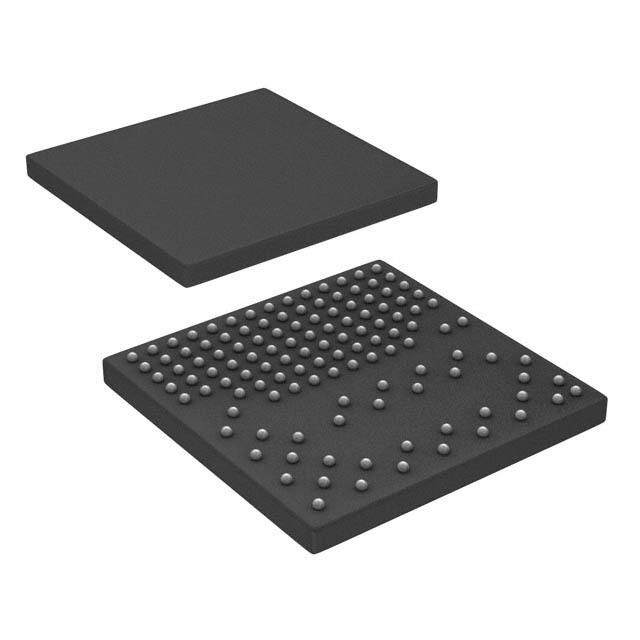
| 产品图片 |
|
| 产品型号 | LTC2641ACMS8-16#PBF |
| rohs | 无铅 / 符合限制有害物质指令(RoHS)规范要求 |
| 产品系列 | - |
| 产品培训模块 | http://www.digikey.cn/PTM/IndividualPTM.page?site=cn&lang=zhs&ptm=19729 |
| 位数 | 16 |
| 供应商器件封装 | 8-MSOP |
| 其它名称 | LTC2641ACMS816PBF |
| 包装 | 管件 |
| 安装类型 | 表面贴装 |
| 封装/外壳 | 8-TSSOP,8-MSOP(0.118",3.00mm 宽) |
| 工作温度 | 0°C ~ 70°C |
| 建立时间 | 1µs |
| 数据接口 | MICROWIRE™,QSPI™,串行,SPI™ |
| 标准包装 | 50 |
| 电压源 | 单电源 |
| 转换器数 | 1 |
| 输出数和类型 | 1 电压 |
| 配用 | /product-detail/zh/DC1096B/DC1096B-ND/3645624 |
| 采样率(每秒) | - |


PDF Datasheet 数据手册内容提取
LTC2641/LTC2642 16-/14-/12-Bit V DACs in OUT 3mm × 3mm DFN FEATURES DESCRIPTION n Tiny 3mm × 3mm 8-Pin DFN Package The LTC®2641/LTC2642 are families of 16-, 14- and 12-bit n Maximum 16-Bit INL Error: ±1LSB over Temperature unbuffered voltage output DACs. These DACs operate from n Low 120µA Supply Current a single 2.7V to 5.5V supply and are guaranteed mono- n Guaranteed Monotonic over Temperature tonic over temperature. The LTC2641A-16/LTC2642A-16 n Low 0.5nV•sec Glitch Impulse provide 16-bit performance (±1LSB INL and ±1LSB DNL) n 2.7V to 5.5V Single Supply Operation over temperature. Unbuffered DAC outputs result in low n Fast 1µs Settling Time to 16 Bits supply current of 120µA and a low offset error of ±1LSB. n Unbuffered Voltage Output Directly Drives 60k Loads Both the LTC2641 and LTC2642 feature a reference input n 50MHz SPI/QSPI/MICROWIRE Compatible range of 2V to V . V swings from 0V to V . For Serial Interface DD OUT REF bipolar operation, the LTC2642 includes matched scaling n Power-On Reset Clears DAC Output to Zero Scale resistors for use with an external precision op amp (such (LTC2641) or Midscale (LTC2642) as the LT1678), generating a ±V output swing at R . n Schmitt-Trigger Inputs for Direct Optocoupler REF FB Interface The LTC2641/LTC2642 use a simple SPI/MICROWIRE n Asynchronous CLR Pin compatible 3-wire serial interface which can be operated n 8-Lead MSOP and 3mm × 3mm DFN Packages at clock rates up to 50MHz and can interface directly (LTC2641) with optocouplers for applications requiring isolation. A n 10-Lead MSOP and 3mm × 3mm DFN Packages power-on reset circuit clears the LTC2641’s DAC output (LTC2642) to zero scale and the LTC2642’s DAC output to midscale when power is initially applied. A logic low on the CLR pin APPLICATIONS asynchronously clears the DAC to zero scale (LTC2641) or midscale (LTC2642). These DACs are all specified over n High Resolution Offset and Gain Adjustment the commercial and industrial ranges. n Process Control and Industrial Automation L, LT, LTC, LTM, Linear Technology and the Linear logo are registered trademarks and n Automatic Test Equipment SoftSpan is a trademark of Linear Technology Corporation. All other trademarks are the n Data Acquisition Systems property of their respective owners. TYPICAL APPLICATION Bipolar 16-Bit DAC LTC2642-16 Integral Nonlinearity 2.7V TO 5.5V VREF 0.1µF 1µF 0.1µF 2V TO VDD 1.0 LTC2642 VDD REF RFB 00..68 ±VV2DR.DE5F V= = R5 2VA.5NVGE 5pF INV – 0.4 16-BIT DAC VOUT +1/2 LT1678 B–VIPROELF ATRO VVORUEFT L (LSB) 0.20 POWER-ON IN –0.2 RESET –0.4 –0.6 CS INL 25°C SCLK 16-BIT DATA LATCH –0.8 INL 90°C DIN CONTROL INL –45°C LOGIC –1.0 CLR 16-BIT SHIFT REGISTER 0 16384 32768 49152 65535 GND CODE 26412 TA01a 26412 TA01b 26412fd 1 For more information www.linear.com/LTC2641
LTC2641/LTC2642 ABSOLUTE MAXIMUM RATINGS (Note 1) V to GND ..................................................–0.3V to 6V Operating Temperature Range DD CS, SCLK, DIN, LTC2641C/LTC2642C ...............................0°C to 70°C CLR to GND .........................–0.3V to (V + 0.3V) or 6V LTC2641I/LTC2642I .............................–40°C to 85°C DD REF, V , INV to GND ........–0.3V to (V + 0.3V) or 6V Maximum Junction Temperature (Note 2) ............125°C OUT DD R to INV .......................................................–6V to 6V Storage Temperature Range ..................–65°C to 150°C FB R to GND .....................................................–6V to 6V Lead Temperature (Soldering, 10 sec) ...................300°C FB GND to GND (S8 Package) OBSOLETE ....–0.3V to 0.3V PIN CONFIGURATION LTC2641 LTC2641 LTC2641 TOP VIEW TOP VIEW REF 1 8 GND TOP VIEW VOUT 1 8 VDD CS 2 7 VDD REF 1 8GND GND 2 7 GND SCLK 3 9 6 VOUT SCCLSK 23 76VVDODUT REF 3 6 DIN DIN 4 5 CLR DIN 4 5CLR CS 4 5 SCLK MS8 PACKAGE S8 PACKAGE 8-LEAD PLASTIC MSOP DD PACKAGE 8-LEAD PLASTIC SO 8-LEAD (3mm × 3mm) PLASTIC DFN TJMAX = 125°C (NOTE 2), θJA = 120°C/W TJMAX = 125°C, θJA = 110°C/W TJMAX = 125°C (NOTE 2), θJA = 43°C/W OBSOLETE PACKAGE EXPOSED PAD (PIN 9) IS GND, MUST BE SOLDERED TO PCB LTC2642 LTC2642 TOP VIEW REF 1 10 GND TOP VIEW CS 2 9 VDD REF 1 10 GND SCLK 3 11 8 RFB SCCLSK 23 98 VRDFBD DIN 4 7 INV DIN 4 7 INV CLR 5 6 VOUT CLR 5 6 VOUT MS PACKAGE DD PACKAGE 10-LEAD PLASTIC MSOP 10-LEAD (3mm × 3mm) PLASTIC DFN TJMAX = 125°C (NOTE 2), θJA = 120°C/W TJMAX = 125°C (NOTE 2), θJA = 43°C/W EXPOSED PAD (PIN 11) IS GND, MUST BE SOLDERED TO PCB 26412fd 2 For more information www.linear.com/LTC2641
LTC2641/LTC2642 ORDER INFORMATION LEAD FREE FINISH TAPE AND REEL PART MARKING* PACKAGE DESCRIPTION TEMPERATURE RANGE LTC2641ACDD-16#PBF LTC2641ACDD-16#TRPBF LCZP 8-Lead (3mm × 3mm) Plastic DFN 0°C to 70°C LTC2641CDD-16#PBF LTC2641CDD-16#TRPBF LCZP 8-Lead (3mm × 3mm) Plastic DFN 0°C to 70°C LTC2641CDD-14#PBF LTC2641CDD-14#TRPBF LCZN 8-Lead (3mm × 3mm) Plastic DFN 0°C to 70°C LTC2641CDD-12#PBF LTC2641CDD-12#TRPBF LCZM 8-Lead (3mm × 3mm) Plastic DFN 0°C to 70°C LTC2641AIDD-16#PBF LTC2641AIDD-16#TRPBF LCZP 8-Lead (3mm × 3mm) Plastic DFN –40°C to 85°C LTC2641IDD-16#PBF LTC2641IDD-16#TRPBF LCZP 8-Lead (3mm × 3mm) Plastic DFN –40°C to 85°C LTC2641IDD-14#PBF LTC2641IDD-14#TRPBF LCZN 8-Lead (3mm × 3mm) Plastic DFN –40°C to 85°C LTC2641IDD-12#PBF LTC2641IDD-12#TRPBF LCZM 8-Lead (3mm × 3mm) Plastic DFN –40°C to 85°C LTC2641ACMS8-16#PBF LTC2641ACMS8-16#TRPBF LTCZS 8-Lead Plastic MSOP 0°C to 70°C LTC2641CMS8-16#PBF LTC2641CMS8-16#TRPBF LTCZS 8-Lead Plastic MSOP 0°C to 70°C LTC2641CMS8-14#PBF LTC2641CMS8-14#TRPBF LTCZR 8-Lead Plastic MSOP 0°C to 70°C LTC2641CMS8-12#PBF LTC2641CMS8-12#TRPBF LTCZQ 8-Lead Plastic MSOP 0°C to 70°C LTC2641AIMS8-16#PBF LTC2641AIMS8-16#TRPBF LTCZS 8-Lead Plastic MSOP –40°C to 85°C LTC2641IMS8-16#PBF LTC2641IMS8-16#TRPBF LTCZS 8-Lead Plastic MSOP –40°C to 85°C LTC2641IMS8-14#PBF LTC2641IMS8-14#TRPBF LTCZR 8-Lead Plastic MSOP –40°C to 85°C LTC2641IMS8-12#PBF LTC2641IMS8-12#TRPBF LTCZQ 8-Lead Plastic MSOP –40°C to 85°C LTC2642ACDD-16#PBF LTC2642ACDD-16#TRPBF LCZW 10-Lead (3mm × 3mm) Plastic DFN 0°C to 70°C LTC2642CDD-16#PBF LTC2642CDD-16#TRPBF LCZW 10-Lead (3mm × 3mm) Plastic DFN 0°C to 70°C LTC2642CDD-14#PBF LTC2642CDD-14#TRPBF LCZV 10-Lead (3mm × 3mm) Plastic DFN 0°C to 70°C LTC2642CDD-12#PBF LTC2642CDD-12#TRPBF LCZT 10-Lead (3mm × 3mm) Plastic DFN 0°C to 70°C LTC2642AIDD-16#PBF LTC2642AIDD-16#TRPBF LCZW 10-Lead (3mm × 3mm) Plastic DFN –40°C to 85°C LTC2642IDD-16#PBF LTC2642IDD-16#TRPBF LCZW 10-Lead (3mm × 3mm) Plastic DFN –40°C to 85°C LTC2642IDD-14#PBF LTC2642IDD-14#TRPBF LCZV 10-Lead (3mm × 3mm) Plastic DFN –40°C to 85°C LTC2642IDD-12#PBF LTC2642IDD-12#TRPBF LCZT 10-Lead (3mm × 3mm) Plastic DFN –40°C to 85°C LTC2642ACMS-16#PBF LTC2642ACMS-16#TRPBF LTCZZ 10-Lead Plastic MSOP 0°C to 70°C LTC2642CMS-16#PBF LTC2642CMS-16#TRPBF LTCZZ 10-Lead Plastic MSOP 0°C to 70°C LTC2642CMS-14#PBF LTC2642CMS-14#TRPBF LTCZY 10-Lead Plastic MSOP 0°C to 70°C LTC2642CMS-12#PBF LTC2642CMS-12#TRPBF LTCZX 10-Lead Plastic MSOP 0°C to 70°C LTC2642AIMS-16#PBF LTC2642AIMS-16#TRPBF LTCZZ 10-Lead Plastic MSOP –40°C to 85°C LTC2642IMS-16#PBF LTC2642IMS-16#TRPBF LTCZZ 10-Lead Plastic MSOP –40°C to 85°C LTC2642IMS-14#PBF LTC2642IMS-14#TRPBF LTCZY 10-Lead Plastic MSOP –40°C to 85°C LTC2642IMS-12#PBF LTC2642IMS-12#TRPBF LTCZX 10-Lead Plastic MSOP –40°C to 85°C OBSOLETE LTC2641CS8-16#PBF LTC2641CS8-16#TRPBF 264116 8-Lead Plastic SO 0°C to 70°C LTC2641IS8-16#PBF LTC2641IS8-16#TRPBF 264116 8-Lead Plastic SO –40°C to 85°C Consult LTC Marketing for parts specified with wider operating temperature ranges. *The temperature grade is identified by a label on the shipping container. Consult LTC Marketing for information on non-standard lead based finish parts. For more information on lead free part marking, go to: http://www.linear.com/leadfree/ For more information on tape and reel specifications, go to: http://www.linear.com/tapeandreel/ 26412fd 3 For more information www.linear.com/LTC2641
LTC2641/LTC2642 ELECTRICAL CHARACTERISTICS The l denotes the specifications which apply over the full operating temperature range, otherwise specifications are at T = 25°C. V = 3V or 5V, V = 2.5V, C = 10pF, GND = 0, R = ∞ unless A DD REF L L otherwise specified. LTC2641-12 LTC2641-14 LTC2641-16 LTC2641A-16 LTC2642-12 LTC2642-14 LTC2642-16 LTC2642A-16 SYMBOL PARAMETER CONDITIONS MIN TYP MAX MIN TYP MAX MIN TYP MAX MIN TYP MAX UNITS Static Performance N Resolution l 12 14 16 16 Bits Monotonicity l 12 14 16 16 Bits DNL Differential Nonlinearity (Note 3) l ±0.5 ±0.5 ±1 ±0.5 ±1 ±0.5 ±1 LSB INL Integral Nonlinearity (Note 3) l ±0.5 ±0.5 ±1 ±0.5 ±2 ±0.5 ±1 LSB ZSE Zero Code Offset Error Code = 0 l 1 2 2 2 LSB ZS Zero Code Tempco ±0.05 ±0.05 ±0.05 ±0.05 ppm/°C TC GE Gain Error l ±0.5 ±2 ±1 ±4 ±2 ±5 ±2 ±5 LSB GE Gain Error Tempco ±0.1 ±0.1 ±0.1 ±0.1 ppm/°C TC R DAC Output Resistance (Note 4) 6.2 6.2 6.2 6.2 kΩ OUT Bipolar Resistor Matching (LTC2642) R /R 1 1 1 1 FB INV Ratio Error (Note 7) l ±0.1 ±0.03 ±0.015 ±0.015 % BZE Bipolar Zero Offset Error (LTC2642) l ±0.5 ±2 ±0.5 ±4 ±2 ±5 ±2 ±5 LSB BZS Bipolar Zero Tempco (LTC2642) ±0.1 ±0.1 ±0.1 ±0.1 ppm/°C TC PSR Power Supply Rejection ΔV = ±10% l ±0.5 ±0.5 ±1 ±1 LSB DD The l denotes the specifications which apply over the full operating temperature range, otherwise specifications are at T = 25°C. A V = 3V or 5V, V = 2.5V, C = 10pF, GND = 0, R = ∞ unless otherwise specified. DD REF L L SYMBOL PARAMETER CONDITIONS MIN TYP MAX UNITS Reference Input V Reference Input Range l 2.0 V V REF DD R Reference Input Resistance (Note 5) Unipolar Mode (LTC2641) l 11 14.8 kΩ REF Bipolar Mode (LTC2642) l 8.5 11.4 kΩ Dynamic Performance—V OUT SR Voltage Output Slew Rate Measured from 10% to 90% 15 V/µs Output Settling Time To ±0.5LSB of FS 1 µs DAC Glitch Impulse Major Carry Transition 0.5 nV•s Digital Feedthrough Code = 0000hex; NCS = V ; 0.2 nV•s DD SCLK, DIN 0V to V Levels DD Output Voltage Noise Density 10 nV/√Hz Dynamic Performance—Reference Input BW Reference –3dB Bandwidth Code = FFFFhex 1.3 MHz Reference Feedthrough Code = 0000hex, V = 1V at 100kHz 1 mV REF P-P P-P SNR Signal-to-Noise Ratio 92 dB C Reference Input Capacitance Code = 0000hex 75 pF IN(REF) Code = FFFFhex 120 pF Digital Inputs V Digital Input High Voltage V = 3.6V to 5.5V l 2.4 V IH CC V = 2.7V to 3.6V l 2.0 V CC 26412fd 4 For more information www.linear.com/LTC2641
LTC2641/LTC2642 ELECTRICAL CHARACTERISTICS The l denotes the specifications which apply over the full operating temperature range, otherwise specifications are at T = 25°C. V = 3V or 5V, V = 2.5V, C = 10pF, GND = 0, R = ∞ unless A DD REF L L otherwise specified. SYMBOL PARAMETER CONDITIONS MIN TYP MAX UNITS V Digital Input Low Voltage V = 4.5V to 5.5V l 0.8 V IL CC V = 2.7V to 4.5V l 0.6 V CC I Digital Input Current V = GND to V l ±1 µA IN IN DD C Digital Input Capacitance (Note 6) l 3 10 pF IN V Hysteresis Voltage 0.15 V H Power Supply V Supply Voltage l 2.7 5.5 V DD I Supply Current, V Digital Inputs = 0V or V l 120 200 µA DD DD DD P Power Dissipation Digital Inputs = 0V or V , V = 5V 0.60 mW D DD DD Digital Inputs = 0V or V , V = 3V 0.36 mW DD DD TIMING CHARACTERISTICS The l denotes the specifications which apply over the full operating temperature range, otherwise specifications are at T = 25°C. V = 3V or 5V, V = 2.5V, C = 10pF, GND = 0, R = ∞ unless otherwise specified. A DD REF L L SYMBOL PARAMETER CONDITIONS MIN TYP MAX UNITS t DIN Valid to SCLK Setup Time l 10 ns 1 t DIN Valid to SCLK Hold Time l 0 ns 2 t SCLK Pulse Width High l 9 ns 3 t SCLK Pulse Width Low l 9 ns 4 t CS Pulse High Width l 10 ns 5 t LSB SCLK High to CS High l 8 ns 6 t CS Low to SCLK High l 8 ns 7 t CS High to SCLK Positive Edge l 8 ns 8 t CLR Pulse Width Low l 15 ns 9 f SCLK Frequency 50% Duty Cycle l 50 MHz SCLK V High to CS Low (Power-Up Delay) 30 µs DD Note 1: Stresses beyond those listed under Absolute Maximum Ratings Note 4: ROUT tolerance is typically ±20%. may cause permanent damage to the device. Exposure to any Absolute Note 5: Reference input resistance is code dependent. Minimum is at Maximum Rating condition for extended periods may affect device 871Chex (34,588) in unipolar mode and at 671Chex (26, 396) in bipolar reliability and lifetime. mode. Note 2: Continuous operation above the specified maximum operating Note 6: Guaranteed by design and not production tested. junction temperature may impair device reliability. Note 7: Guaranteed by gain error and offset error testing, not production Note 3: LTC2641-16/LTC2642-16 ±1LSB = ±0.0015% = ±15.3ppm of full tested. scale. LTC2641-14/LTC2642-14 ±1LSB = ±0.006% = ±61ppm of full scale. LTC2641-12/LTC2642-12 ±1LSB = ±0.024% = ±244ppm of full scale. 26412fd 5 For more information www.linear.com/LTC2641
LTC2641/LTC2642 TYPICAL PERFORMANCE CHARACTERISTICS Integral Nonlinearity (INL) Integral Nonlinearity (INL) vs Supply (V ) INL vs V DD REF 1.0 1.0 1.0 LTC2642-16 VREF = 2.5V VDD = 5.5V 0.8 0.8 0.8 VREF = 2.5V 0.6 VDD = 5V 0.6 0.6 0.4 0.4 +INL 0.4 +INL B) 0.2 B) 0.2 B) 0.2 S S S L (L 0 L (L 0 L (L 0 IN–0.2 IN–0.2 –INL IN–0.2 –INL –0.4 –0.4 –0.4 –0.6 –0.6 –0.6 –0.8 –0.8 –0.8 –1.0 –1.0 –1.0 0 16384 32768 49152 65535 2 3 4 5 6 2 3 4 5 6 CODE VDD (V) VREF (V) 26412 G01 26412 G02 26412 G03 Differential Nonlinearity (DNL) Differential Nonlinearity (DNL) vs Supply (V ) DNL vs V DD REF 1.0 1.0 1.0 LTC2642-16 VREF = 2.5V VDD = 5.5V 0.8 0.8 0.8 VREF = 2.5V 0.6 VDD = 5V 0.6 0.6 0.4 0.4 0.4 B) 0.2 B) 0.2 +DNL B) 0.2 +DNL S S S L (L 0 L (L 0 –DNL L (L 0 –DNL N N N D–0.2 D–0.2 D–0.2 –0.4 –0.4 –0.4 –0.6 –0.6 –0.6 –0.8 –0.8 –0.8 –1.0 –1.0 –1.0 0 16384 32768 49152 65535 2 3 4 5 6 2 3 4 5 6 CODE VDD (V) VREF (V) 26412 G04 26412 G05 26412 G06 INL vs Temperature DNL vs Temperature Bipolar Zero Error vs Temperature 1.0 1.0 5 VREF = 2.5V VREF = 2.5V VREF = 2.5V 0.8 VDD = 5V 0.8 VDD = 5V 4 VDD = 5V 0.6 0.6 3 0.4 +INL 0.4 2 INL (LSB)–00..220 –INL DNL (LSB)–00..220 +–DDNNLL BZE (LSB) –110 –0.4 –0.4 –2 –0.6 –0.6 –3 –0.8 –0.8 –4 –1.0 –1.0 –5 –40 –15 10 35 60 85 –40 –15 10 35 60 85 –40 –15 10 35 60 85 TEMPERATURE (°C) TEMPERATURE (°C) TEMPERATURE (°C) 26412 G07 26412 G08 26412 G09 26412fd 6 For more information www.linear.com/LTC2641
LTC2641/LTC2642 TYPICAL PERFORMANCE CHARACTERISTICS Unbuffered Zero Scale Error vs Unbuffered Full-Scale Error vs Bipolar Gain Error vs Temperature Temperature (LTC2641-16) Temperature (LTC2641-16) 5 1.0 1.0 VREF = 2.5V 4 VDD = 5V 0.8 0.8 3 0.6 0.6 2 0.4 0.4 B) 1 B) 0.2 B) 0.2 S S S GE (L 0 SE (L 0 SE (L 0 B –1 Z–0.2 F–0.2 –2 –0.4 –0.4 –3 –0.6 –0.6 –4 –0.8 –0.8 –5 –1.0 –1.0 –40 –15 10 35 60 85 –40 –15 10 35 60 85 –40 –15 10 35 60 85 TEMPERATURE (°C) TEMPERATURE (°C) TEMPERATURE (°C) 26412 G10 26412 G11 26412 G12 14-Bit Integral Nonlinearity (INL) 14-Bit Differential Nonlinearity (LTC2642-14) (DNL) (LTC2642-14) I vs Code (Unipolar LTC2641) REF 1.0 1.0 250 LTC2642-14 LTC2642-14 VREF = 2.5V 0.8 0.8 VREF = 2.5V VREF = 2.5V 0.6 VDD = 5V 0.6 VDD = 5V 200 0.4 0.4 INL (LSB)–00..220 DNL (LSB)–00..220 I (µA) REF 110500 –0.4 –0.4 –0.6 –0.6 50 –0.8 –0.8 –1.0 –1.0 0 0 4096 8192 12288 16383 0 4096 8192 12288 16383 0 16384 32768 49152 65535 CODE CODE CODE 26412 G13 26412 G14 26412 G15 12-Bit Integral Nonlinearity (INL) 12-Bit Differential Nonlinearity (LTC2642-12) (DNL) (LTC2642-12) I vs Code (Bipolar LTC2642) REF 1.0 1.0 250 LTC2642-12 LTC2642-12 VREF = 2.5V 0.8 0.8 VREF = 2.5V VREF = 2.5V 0.6 VDD = 5V 0.6 VDD = 5V 200 0.4 0.4 INL (LSB)–00..220 DNL (LSB)–00..220 I (µA) REF 110500 –0.4 –0.4 –0.6 –0.6 50 –0.8 –0.8 –1.0 –1.0 0 0 1024 2048 3072 4095 0 1024 2048 3072 4095 0 16384 32768 49152 65535 CODE CODE CODE 26412 G16 26412 G17 26412 G18 26412fd 7 For more information www.linear.com/LTC2641
LTC2641/LTC2642 TYPICAL PERFORMANCE CHARACTERISTICS Supply Current (I ) vs Supply Current (I ) vs Supply Supply Current (I ) vs Digital DD DD DD Temperature Voltage (V ) Input Voltage DD 150 150 900 VREF = 2.5V VREF = 2.5V 800 125 125 VDD = 5V 700 VDD = 5V 100 100 600 VDD = 3V A) A) A)500 (µDD 75 (µDD 75 (µDD400 I I I 50 50 300 VDD = 3V 200 25 25 100 0 0 0 –40 –15 10 35 60 85 2.5 3 3.5 4 4.5 5 5.5 0 0.5 1 1.5 2 2.5 3 3.5 4 4.5 5 TEMPERATURE (°C) VDD (V) DIGITAL INPUT VOLTAGE (V) 26412 G19 26412 G20 26412 G21 Supply Current (I ) vs V , Supply Current (I ) vs V , DD REF DD REF V = 5V V = 3V Midscale Glitch Impulse DD DD 150 150 VDD = 5V VDD = 3V CS 5V/DIV 125 125 CODE CODE CODE 100 100 32767 32768 32767 VOUT A) A) 20mV/DIV (µD 75 (µD 75 D D I I 50 50 25 25 LTC2641-16 500ns/DIV 26412 G24 UNBUFFERED 0 0 CL = 10pF 1 1.5 2 2.5 3 3.5 4 4.5 5 1 1.5 2 2.5 3 VREF (V) VREF (V) 26412 G22 26412 G23 V vs V = 0V to 5.5V OUT DD Full-Scale Transition Full-Scale Settling (Zoomed In) (POR Function) LTC2641 CS 5V/DIV CS VDD = VREF 5V/DIV 0V TO 5.5V SETTLE 2V/DIV RESIDUE VOUT 250µV/DIV VOUT 1V/DIV 10mV/DIV LTC2641-16 500ns/DIV 26412 G25 LTC2641-16 500ns/DIV 26412 G26 LTC2641-16 50ms/DIV 26412 G27 UNBUFFERED VREF = 2.5V UNBUFFERED CL = 10pF CONSULT FACTORY FOR CL = 10pF VREF = 2.5V MEASUREMENT CIRCUIT VDD = 5V 26412fd 8 For more information www.linear.com/LTC2641
LTC2641/LTC2642 PIN FUNCTIONS LTC2641 – MSOP, DFN Packages GND (Pin 7): Circuit Ground Pin. Must be connected to Pin 2 (GND). REF (Pin 1): Reference Voltage Input. Apply an external reference at REF between 2V and V . V (Pin 8): Supply Voltage. Set between 2.7V and 5.5V. DD DD CS (Pin 2): Serial Interface Chip Select/Load Input. When LTC2642 – MSOP, DFN Packages CS is low, SCLK is enabled for shifting in data on DIN. When CS is taken high, SCLK is disabled, the 16-bit input REF (Pin 1): Reference Voltage Input. Apply an external word is latched and the DAC is updated. reference at REF between 2V and VDD. SCLK (Pin 3): Serial Interface Clock Input. CMOS and CS (Pin 2): Serial Interface Chip Select/Load Input. When TTL compatible. CS is low, SCLK is enabled for shifting in data on DIN. When CS is taken high, SCLK is disabled, the 16-bit input DIN (Pin 4): Serial Interface Data Input. Data is applied to word is latched and the DAC is updated. DIN for transfer to the device at the rising edge of SCLK. SCLK (Pin 3): Serial Interface Clock Input. CMOS and CLR (Pin 5): Asynchronous Clear Input. A logic low clears TTL compatible. the DAC to code 0. DIN (Pin 4): Serial Interface Data Input. Data is applied to V (Pin 6): DAC Output Voltage. The output range is OUT DIN for transfer to the device at the rising edge of SCLK. 0V to V . REF CLR (Pin 5): Asynchronous Clear Input. A logic low clears V (Pin 7): Supply Voltage. Set between 2.7V and 5.5V. DD the DAC to midscale. GND (Pin 8): Circuit Ground. V (Pin 6): DAC Output Voltage. The output range is OUT Exposed Pad (DFN Pin 9): Circuit Ground. Must be sol- 0V to V . REF dered to PCB ground. INV (Pin 7): Center Tap of Internal Scaling Resistors. Connect to an external amplifier’s inverting input in bi- LTC2641 – SO Package OBSOLETE polar mode. V (Pin 1): DAC Output Voltage. The output range is OUT R (Pin 8): Feedback Resistor. Connect to an external 0V to V . FB REF amplifier’s output in bipolar mode. The bipolar output GND (Pin 2): Circuit Ground. range is –V to V . REF REF REF (Pin 3): Reference Voltage Input. Apply an external V (Pin 9): Supply Voltage. Set between 2.7V and 5.5V. DD reference at REF between 2V and V . DD GND (Pin 10): Circuit Ground. CS (Pin 4): Serial Interface Chip Select/Load Input. When Exposed Pad (DFN Pin 11): Circuit Ground. Must be CS is low, SCLK is enabled for shifting in data on DIN. soldered to PCB ground. When CS is taken high, SCLK is disabled, the 16-bit input word is latched and the DAC is updated. SCLK (Pin 5): Serial Interface Clock Input. CMOS and TTL compatible. DIN (Pin 6): Serial Interface Data Input. Data is applied to DIN for transfer to the device at the rising edge of SCLK. 26412fd 9 For more information www.linear.com/LTC2641
LTC2641/LTC2642 BLOCK DIAGRAMS LTC2641 - MSOP, DFN LTC2641 - SO OBSOLETE PACKAGE 7 1 8 3 VDD REF VDD REF LTC2641-16 LTC2641-16 LTC2641-14 LTC2641-12 POWER-ON VOUT POWER-ON VOUT RESET 16-/14-/12-BIT DAC 6 RESET 16-/14-/12-BIT DAC 1 CS CS 2 4 SCLK SCLK 3 CONTROL 16-BIT DATA LATCH 5 CONTROL 16-BIT DATA LATCH 4 DIN LOGIC 6 DIN LOGIC 5 CLR 16-BIT SHIFT REGISTER GND 7 GND 16-BIT SHIFT REGISTER GND 8 2641 BD01a 2 2641 BD01b LTC2642 9 1 VDD REF RFB LTC2642-16 8 LTC2642-14 INV LTC2642-12 7 POWER-ON VOUT RESET 16-/14-/12-BIT DAC 6 CS 2 SCLK 3 CONTROL 16-BIT DATA LATCH DIN LOGIC 4 5 CLR 16-BIT SHIFT REGISTER GND 10 2642 BD 26412fd 10 For more information www.linear.com/LTC2641
LTC2641/LTC2642 TIMING DIAGRAM t1 t2 t3 t4 t6 SCK 1 2 3 15 16 t8 SDI t5 t7 CS/LD 26412 TD OPERATION General Description The digital-to-analog transfer function at the V pin is: OUT The LTC2641/LTC2642 family of 16-/14-/12-bit voltage k V = V output DACs offer full 16-bit performance with less than OUT(IDEAL) 2N REF ±1LSB integral linearity error and less than ±1LSB differ- ential linearity error, guaranteeing monotonic operation. where k is the decimal equivalent of the binary DAC input They operate from a single supply ranging from 2.7V to code, N is the resolution, and V is between 2.0V and REF 5.5V, consuming 120µA (typical). An external voltage V (see Tables 1a, 1b and 1c). DD reference of 2V to V determines the DAC’s full-scale DD The LTC2642 includes matched resistors that are tied output voltage. A 3-wire serial interface allows the LTC2641/ to an external amplifier to provide bipolar output swing LTC2642 to fit into a small 8-/10-pin MSOP or DFN 3mm (Figure 2). The bipolar transfer function at the RFB pin is: × 3mm package. k Digital-to-Analog Architecture VOUT_BIPOLAR(IDEAL) =VREF2N–1 –1 The DAC architecture is a voltage switching mode resis- tor ladder using precision thin-film resistors and CMOS (see Tables 2a, 2b and 2c). switches. The LTC2641/LTC2642 DAC resistor ladders are Serial Interface composed of a proprietary arrangement of matched DAC sections. The four MSBs are decoded to drive 15 equally The LTC2641/LTC2642 communicates via a standard weighted segments, and the remaining lower bits drive 3-wire SPI/QSPI/MICROWIRE compatible interface. The successively lower weighted sections. Major carry glitch chip select input (CS) controls and frames the loading of impulse is very low at 500pV•sec, CL = 10pF, ten times serial data from the data input (DIN). Following a CS high- lower than previous DACs of this type. to-low transition, the data on DIN is loaded, MSB first, into the shift register on each rising edge of the serial clock 26412fd 11 For more information www.linear.com/LTC2641
LTC2641/LTC2642 OPERATION input (SCLK). After 16 data bits have been loaded into the Power-On Reset serial input register, a low-to-high transition on CS trans- The LTC2641/LTC2642 include a power-on reset circuit fers the data to the 16-bit DAC latch, updating the DAC to ensure that the DAC output comes up in a known output (see Figures 1a, 1b, 1c). While CS remains high, state. When V is first applied, the power-on reset cir- DD the serial input shift register is disabled. If there are less cuit sets the output of the LTC2641 to zero-scale (code than 16 low-to-high transitions on SCLK while CS remains 0). The LTC2642 powers up to midscale (bipolar zero). low, the data will be corrupted, and must be reloaded. Depending on the DAC number of bits, the midscale code Also, if there are more than 16 low-to-high transitions is: 32,768 (LTC2642-16); 8,192 (LTC2642-14); or 2,048 on SCLK while CS remains low, only the last 16 data bits (LTC2642-12). loaded from DIN will be transferred to the DAC latch. For the 14-bit DACs, (LTC2641-14/LTC2642-14), the MSB Clearing the DAC remains in the same (left-justified) position in the input A low pulse meeting the t (minimum) specification on 16-bit data word. Therefore, two “don’t-care” bits must 9 the CLR pin asynchronously clears the DAC latch to code be loaded after the LSB, to make up the required 16 data zero (LTC2641) or to midscale (LTC2642). bits (Figure 1b). Similarly, for the 12-bit family members (LTC2641-12/LTC2642-12) four “don’t-care” bits must follow the LSB (Figure 1c). CS DAC SCLK 1 2 3 4 5 6 7 8 9 10 11 12 13 14 15 16 UPDATED DIN D15 D14 D13 D12 D11 D10 D9 D8 D7 D6 D5 D4 D3 D2 D1 D0 MSB LSB 26412 F01a DATA (16 BITS) Figure 1a. 16-Bit Timing Diagram (LTC2641-16/LTC2642-16) CS DAC SCLK 1 2 3 4 5 6 7 8 9 10 11 12 13 14 15 16 UPDATED DIN D13 D12 D11 D10 D9 D8 D7 D6 D5 D4 D3 D2 D1 D0 X X MSB LSB 26412 F01b DATA (14 BITS + 2 DON’T-CARE BITS) Figure 1b. 14-Bit Timing Diagram (LTC2641-14/LTC2642-14) CS DAC SCLK 1 2 3 4 5 6 7 8 9 10 11 12 13 14 15 16 UPDATED DIN D11 D10 D9 D8 D7 D6 D5 D4 D3 D2 D1 D0 X X X X MSB LSB 26412 F01c DATA (12 BITS + 4 DON’T-CARE BITS) Figure 1c. 12-Bit Timing Diagram (LTC2641-12/LTC2642-12) 26412fd 12 For more information www.linear.com/LTC2641
LTC2641/LTC2642 APPLICATIONS INFORMATION Unipolar Configuration The external amplifier provides a unity-gain buffer. The LTC2642 can also be used in unipolar configuration by Figure 2 shows a typical unipolar DAC application for tying R and INV to REF . This provides power-up and the LTC2641. Tables 1a, 1b and 1c show the unipolar FB clear to midscale. binary code tables for 16-bit, 14-bit and 12-bit operation. VREF 2.5V OUT IN 5V 0.1µF 4.7µF LT®1019CS8-2.5 Table 1a. 16-Bit Unipolar Binary Code Table 5V/3V GND (LTC2641-16) DIGITAL INPUT 0.1µF BINARY NUMBER ANALOG OUTPUT 7 1 5V/3V 0.1µF IN DAC LATCH (V ) OUT VDD REF MSB LSB – LTC2641-16 1/2 LTC6078 UNIPOLAR VOUT 1111 1111 1111 1111 VREF (65,535/65,536) 0V TO 2.5V 2 CS 16-BIT DAC VOUT 6 + 1000 0000 0000 0000 VREF (32,768/65,536) = VREF/2 3 SCLK 0000 0000 0000 0001 VREF (1/65,536) 4 DIN 0000 0000 0000 0000 0V 5 CLR GND 26412 F02 8 Figure 2. 16-Bit Unipolar Output (LTC2641-16) Unipolar V = 0V to V OUT REF Table 1b. 14-Bit Unipolar Binary Code Table Table 1c. 12-Bit Unipolar Binary Code Table (LTC2641-14) (LTC2641-12) DIGITAL INPUT DIGITAL INPUT BINARY NUMBER ANALOG OUTPUT BINARY NUMBER ANALOG OUTPUT IN DAC LATCH (V ) IN DAC LATCH (V ) OUT OUT MSB LSB MSB LSB 1111 1111 1111 11xx V (16,383/16,384) 1111 1111 1111 xxxx V (4,095/4,096) REF REF 1000 0000 0000 00xx V (8,192/16,384) = V /2 1000 0000 0000 xxxx V (2,048/4,096) = V /2 REF REF REF REF 0000 0000 0000 01xx V (1/16,384) 0000 0000 0001 xxxx V (1/4,096) REF REF 0000 0000 0000 00xx 0V 0000 0000 0000 xxxx 0V 26412fd 13 For more information www.linear.com/LTC2641
LTC2641/LTC2642 APPLICATIONS INFORMATION Bipolar Configuration The amplifier circuit provides a gain of +2 from the V OUT pin, and gain of –1 from V . Tables 2a, 2b and 2c show Figure 3 shows a typical bipolar DAC application for the REF the bipolar offset binary code tables for 16-bit, 14-bit and LTC2642. The on-chip bipolar offset/gain resistors, R FB 12-bit operation. and R , are connected to an external amplifier to produce INV a bipolar output swing from –V to V at the R pin. REF REF FB VREF 5V/3V 2.5V OUT IN 5V 0.1µF 0.1µF 4.7µF LT1019CS8-2.5 9 1 GND VDD REF RFB 8 5V 0.1µF LTC2642-16 C1 10pF INV 7 – 1/2 LT1678 BIPOLAR VOUT –2.5V TO 2.5V 2 CS 16-BIT DAC VOUT 6 + 0.1µF 3 SCLK 4 –5V DIN 5 CLR GND 26412 F02 10 Figure 3. 16-Bit Bipolar Output (LTC2642-16) V = –V to V OUT REF REF Table 2a. 16-Bit Bipolar Offset Binary Table 2b. 14-Bit Bipolar Offset Binary Table 2c. 12-Bit Bipolar Offset Binary Code Table (LTC2642-16) Code Table (LTC2642-14) Code Table (LTC2642-12) DIGITAL INPUT DIGITAL INPUT DIGITAL INPUT BINARY NUMBER ANALOG OUTPUT BINARY NUMBER ANALOG OUTPUT BINARY NUMBER ANALOG OUTPUT IN DAC LATCH (V ) IN DAC LATCH (V ) IN DAC LATCH (V ) OUT OUT OUT MSB LSB MSB LSB MSB LSB 1111 1111 1111 1111 V (32,767/32,768) 1111 1111 1111 11xx V (8,191/8,192) 1111 1111 1111 xxxx V (2,047/2,048) REF REF REF 1000 0000 0000 0001 V (1/32,768) 1000 0000 0000 01xx V (1/8,192) 1000 0000 0001 xxxx V (1/2,048) REF REF REF 1000 0000 0000 0000 0V 1000 0000 0000 00xx 0V 1000 0000 0000 xxxx 0V 0111 1111 1111 1111 –V (1/32,768) 0111 1111 1111 11xx –V (1/8,192) 0111 1111 1111 xxxx –V (1/2048) REF REF REF 0000 0000 0000 0000 –V 0000 0000 0000 00xx –V 0000 0000 0000 xxxx –V REF REF REF 26412fd 14 For more information www.linear.com/LTC2641
LTC2641/LTC2642 APPLICATIONS INFORMATION Unbuffered Operation and V Loading Unbuffered V Settling Time OUT OUT The DAC output is available directly at the V pin, which The settling time at the V pin can be closely approxi- OUT OUT swings from GND to V . Unbuffered operation provides mated by a single-pole response where: REF the lowest possible offset, full-scale and linearity errors, t = R • (C + C ) the fastest settling time and minimum power consumption. OUT OUT L (Figure 4). Settling to 1/2LSB at 16-bits requires about However, unbuffered operation requires that appropriate 12 time constants (ln(2 • 65,536)). The typical settling loading be maintained on the V pin. The LTC2641/ OUT time of 1µs corresponds to a time constant of 83ns, and LTC2642 V can be modeled as an ideal voltage source OUT a total (C + C ) of about 83ns/6.2k = 13pF . The internal in series with a source resistance of R , typically 6.2k OUT L OUT capacitance, C is typically 10pF, so an external C of (Figure 4). The DAC’s linear output impedance allows it to OUT L 3pF corresponds to 1µs settling to 1/2LSB. drive medium loads (R > 60k) without degrading INL or L DNL; only the gain error is increased. The gain error (GE) VREF caused by a load resistance, R , (relative to full scale) is: L –1 LTC2641 REF GE= 1+RROLUT VLTRCE2F6(C42O2NDE)–+ ROUT CVOOUUTT RL CL ILV0VO UTTO VREF GND 26412 F04 In 16-bit LSBs: Figure 4. V Pin Equivalent Circuit –65536 OUT GE= (cid:31)LSB R 1+ OUT Op Amp Selection R L The optimal choice for an external buffer op amp depends R has a low tempco (typically < ±50ppm/°C), and is on whether the DAC is used in the unipolar or bipolar OUT independent of DAC code. The variation of R , part-to- mode of operation, and also depends on the accuracy, OUT part, is typically less than ±20%. speed, power dissipation and board area requirements of the application. The LTC2641/LTC2642’s combination of Note on LSB units: tiny package size, rail-to-rail single supply operation, low For the following error descriptions, “LSB” means 16-bit power dissipation, fast settling and nearly ideal accuracy LSB and 65,536 is rounded to 66k. specifications makes it impractical for one op amp type to fit every application. To convert to 14-bit LSBs (LTC2641-14/LTC2642-14) divide by 4. In bipolar mode (LTC2642 only), the amplifier operates with the internal resistors to provide bipolar offset and To convert to 12-bit LSBs (LTC2641-12/LTC2642-12) scaling. In this case, a precision amplifier operating from divide by 16. dual power supplies, such as the the LT1678 provides the A constant current, I , loading V will produce an offset of: L OUT ±V output range (Figure 3). REF V = –I • R OFFSET L OUT In unipolar mode, the output amplifier operates as a unity For V = 2.5V, a 16-bit LSB equals 2.5V/65,536, or gain voltage follower. For unipolar, single supply applica- REF 38µV. Since R is 6.2k, an I of 6nA produces an offset tions a precision, rail-to-rail input, single supply op amp OUT L of 1LSB. Therefore, to avoid degrading DAC performance, it is critical to protect the V pin from any sources of OUT leakage current. 26412fd 15 For more information www.linear.com/LTC2641
LTC2641/LTC2642 APPLICATIONS INFORMATION such as the LTC6078 is suitable, if the application does voltage temperature coefficient (referenced to 25°C) of not require linear operation very near to GND, or zero scale 0.6μV/°C will add 1LSB of zero-scale error. Also, I and BIAS (Figure 2). The LTC6078 typically swings to within 1mV of the V error it causes, will typically show significant OFFSET GND if it is not required to sink any load current. For an relative variation over temperature. LSB size of 38µV, 1mV represents 26 missing codes near Op amp open-loop gain, A , contributes to DAC gain VOL zero scale. Linearity will be degraded over a somewhat error (GE): larger range of codes above GND. It is also unavoidable that settling time and transient performance will degrade 66k GE= [LSB] whenever a single supply amplifier is operated very close A VOL to GND, or to the positive supply rail. Op amp input common mode rejection ratio (CMRR) is an The small LSB size of a 16-bit DAC, coupled with the tight input-referred error that corresponds to a combination of accuracy specifications on the LTC2641/LTC2642, means gain error (GE) and INL, depending on the op amp archi- that the accuracy and input specifications for the external tecture and operating conditions. A conservative estimate op amp are critical for overall DAC performance. of total CMRR error is: Op Amp Specifications and Unipolar DAC Accuracy CMRR V Most op amp accuracy specifications convert easily to Error=10 20 (cid:127) CMRR_RANGE(cid:127)66k(cid:31)LSB DAC accuracy. VREF Op amp input bias current on the noninverting (+) input is equivalent to an I loading the DAC V pin and therefore where V is the voltage range that CMRR (in L OUT CMRR_RANGE produces a DAC zero-scale error (ZSE) (see Unbuffered dB) is specified over. Op amp Typical Performance Char- Operation): acteristics graphs are useful to predict the impact of CMRR errors on DAC performance. Typically, a precision op amp ZSE = –I (IN+) • R [Volts] B OUT will exhibit a fairly linear CMRR behavior (corresponding In 16-bit LSBs: to DAC gain error only) over most of the common mode input range (CMR), and become nonlinear and produce ZSE=–IB(IN+)(cid:127)6.2k(cid:127)66k (cid:31)LSB significant errors near the edge of the CMR. V REF Rail-to-rail input op amps are a special case, because they Op amp input impedance, R , is equivalent to an R have 2 distinct input stages, one with CMR to GND and IN L loading the LTC2641/LTC2642 V pin, and produces the other with CMR to V+. This results in a “crossover” OUT a gain error of: CM input region where operation switches between the two input stages. –66k GE= (cid:31)LSB The LTC6078 rail-to-rail input op amp typically exhibits 6.2k 1+ remarkably low crossover linearity error, as shown in the R IN VOS vs VCM Typical Performance Characteristics graphs (see the LTC6078 data sheet). Crossover occurs at CM Op amp offset voltage, V , corresponds directly to DAC OS inputs about 1V below V+, and an LTC6078 operating as zero code offset error, ZSE: a unipolar DAC buffer with V = 2.5V and V+ = 5V will REF 66k typically add only about 1LSB of GE and almost no INL ZSE= VOS (cid:127) [LSB] error due to CMRR. Even in a full rail-to-rail application, V REF with V = V+ = 5V, a typical LTC6078 will add only about REF Temperature effects also must be considered. Over the 1LSB of INL at 16-bits. –40°C to 85°C industrial temperature range, an offset 26412fd 16 For more information www.linear.com/LTC2641
LTC2641/LTC2642 APPLICATIONS INFORMATION Op Amp Specifications and Bipolar DAC Accuracy will introduce a feedback loop pole with a time constant of (C • 28k/2). A small feedback capacitor, C1, should be The op amp contributions to unipolar DAC error discussed P included, to introduce a zero that will partially cancel this above apply equally to bipolar operation. The bipolar ap- pole. C1 should nominally be <C , typically in the range plication circuit gains up the DAC span, and all errors, by P of 5pF to 10pF . This will restore the phase margin and a factor of 2. Since the LSB size also doubles, the errors improve coarse settling time, but a pole-zero doublet will in LSBs are identical in unipolar and bipolar modes. unavoidably leave a slower settling tail, with a time con- One added error in bipolar mode comes from I (IN–), stant of roughly (C + C1) • 28k/2, which will limit 16-bit B P which flows through R to generate an offset. The full settling time to be greater than 2µs. FB bias current offset error becomes: Reference and GND Input V = (I (IN–) • R – I (IN+) • R • 2) [Volts] OFFSET B FB B OUT The LTC2641/LTC2642 operates with external voltage refer- So: ences from 2V to V , and linearity, offset and gain errors DD ( – + ) 33k are virtually unchanged vs VREF . Full 16-bit performance V = I (IN )(cid:127)28k–I (IN )(cid:127)12.4k (cid:127) [LSB] OFFSET B B V can be maintained if appropriate guidelines are followed REF when selecting and applying the reference. The LTC2641/ Settling Time with Op Amp Buffer LTC2642’s very low gain error tempco of 0.1ppm/°C, typ- ical, corresponds to less than 0.5LSB variation over the When using an external op amp, the output settling time –40°C to 85°C temperature range. In practice, this means will still include the single pole settling on the LTC2641/ that the overall gain error tempco will be determined almost LTC2642 V node, with time constant R • (C + OUT OUT OUT entirely by the external reference tempco. C ) (see Unbuffered V Settling Time). C will include L OUT L the buffer input capacitance and PC board interconnect The DAC voltage-switching mode “inverted” resistor lad- capacitance. der architecture used in the LTC2641/LTC2642 exhibits a reference input resistance (R ) that is code dependent REF The external buffer amplifier adds another pole to the output (see the Typical Performance curves I vs Input Code). response, with a time constant equal to (fbandwidth/2π). REF For example, assume that CL is maintained at the same In unipolar mode, the minimum RREF is 14.8k (at code value as above, so that the VOUT node time constant is 871Chex, 34,588 decimal) and the the maximum RREF is 83ns = 1μs/12. The output amplifier pole will also have a 300k at code 0000hex (zero scale). The maximum change time constant of 83ns if the closed-loop bandwidth equals in IREF for a 2.5V reference is 160µA. Since the maximum (1/2π • 83ns) = 1.9MHz. The effective time constant of occurs near midscale, the INL error is about one half of the two cascaded single-pole sections is approximately the change on VREF , so maintaining an INL error of <0.1LSB root square sum of the individual time constants, or √2 requires a reference load regulation of (1.53ppm • 2/160µA) • 83ns = 117ns, and 1/2 LSB settling time will be ~12 • = 19 [ppm/mA]. This implies a reference output impedance 117ns = 1.4μs. This represents an ideal case, with no slew of 48mΩ, including series wiring resistance. limiting and ideal op amp phase margin. In practice, it To prevent output glitches from occurring when resistor will take a considerably faster amplifier, as well as careful ladder branches switch from GND to V , the reference REF attention to maintaining good phase margin, to approach input must maintain low impedance at higher frequencies. the unbuffered settling time of 1μs. A 0.1μF ceramic capacitor with short leads between REF The output settling time for bipolar applications (Fig- and GND provides high frequency bypassing. A surface ure 3) will be somewhat increased due to the feedback mount ceramic chip capacitor is preferred because it has resistor network R and R (each 28k nominal). The the lowest inductance. An additional 1μF between REF FB INV parasitic capacitance, C , on the op amp (–) input node and GND provides low frequency bypassing. The circuit P 26412fd 17 For more information www.linear.com/LTC2641
LTC2641/LTC2642 APPLICATIONS INFORMATION will benefit from even higher bypass capacitance, as long should be used, with analog and digital signals carefully as the external reference remains stable with the added routed over separate areas of the plane. This keeps digital capacitive loading. signals away from sensitive analog signals and minimizes the interaction between digital ground currents and the Digital Inputs and Interface Logic analog section of the ground plane. All of the digital inputs include Schmitt-trigger buffers to A “star ground” area should be established by attaching accept slow transition interfaces. This means that opto- the LTC2641/LTC2642 GND pin, V GND and the DAC REF cuplers can interface directly to the LTC2641/LTC2642 V GND reference terminal to the same area on the OUT without additional external logic. Digital input hysteresis GND plane. Care should be taken to ensure that no large is typically 150mV. GND return current paths flow through the “star GND” area. In particular, the resistance from the LTC2641 GND The digital inputs are compatible with TTL/CMOS-logic pin to the point where the V input source connects to levels. However, rail-to-rail (CMOS) logic swings are REF the ground plane should be as low as possible. Excessive preferred, because operating the logic inputs away from resistance here will be multiplied by the code dependent the supply rails generates additional I and GND current, DD I current to produce an INL error similar to the error (see Typical Performance Characteristic graph Supply REF produced by V source resistance. For the LTC2641 in Current vs Logic Input Voltage). REF the S8 package both GND pins, Pin 2 and Pin 7 should Digital feedthrough is only 0.2nV•s typical, but it is always be tied to the same GND plane. preferred to keep all logic inputs static except when loading Sources of ground return current in the analog area include a new code into the DAC. op amp power supply bypass capacitors and the GND Board Layout for Precision connection for single supply amps. A useful technique for minimizing errors is to use a separate board layer for Even a small amount of board leakage can degrade power ground return connections, and reserve one ground accuracy. The 6nA leakage current into V needed to OUT plane layer for low current “signal” GND connections. generate 1LSB offset error corresponds to 833MΩ leakage The “signal”, or “star” GND plane must connected to the resistance from a 5V supply. “power” GND plane at a single point, which should be The V node is relatively sensitive to capacitive noise located near the LTC2641/LTC2642 GND pin. OUT coupling, so minimum trace length, appropriate shielding If separate analog and digital ground areas exist it is neces- and clean board layout are imperative here. sary to connect them at a single location, which should be Temperature differences at the DAC, op amp or reference fairly close to the DAC for digital signal integrity. In some pins can easily generate tens of microvolts of thermocou- systems, large GND return currents can flow between the ple voltages. Analog signal traces should be short, close digital and analog GNDs, especially if different PC boards together and away from heat dissipating components. Air are involved. In such cases the digital and analog ground currents across the board can also generate thermocouples. connection point should not be made right at the “star” GND area, so the highly sensitive analog signals are not The PC board should have separate areas for the analog and corrupted. If forced to choose, always place analog ground digital sections of the circuit. A single, solid ground plane quality ahead of digital signal ground. (A few mV of noise 26412fd 18 For more information www.linear.com/LTC2641
LTC2641/LTC2642 APPLICATIONS INFORMATION on the digital inputs is imperceptible, thanks to the digital Caution: if a GND plane gap is improperly placed, so that input hysteresis) it interrupts a significant GND return path, or if a signal traces crosses over the gap, then adding the gap may Just by maintaining separate areas on the GND plane greatly degrade performance! In this case, the GND and where analog and digital return currents naturally flow, signal return currents are forced to flow the long way good results are generally achieved. Only after this has around the gap, and then are typically channeled directly been done, it is sometimes useful to interrupt the ground into the most sensitive area of the analog GND plane. plane with strategically placed “slots”, to prevent the digital ground currents from fringing into the analog portion of the plane. When doing this, the gap in the plane should be only as long as it needs to be to serve its purpose. PACKAGE DESCRIPTION Please refer to http://www.linear.com/designtools/packaging/ for the most recent package drawings. DD Package 8-Lead Plastic DFN (3mm × 3mm) (Reference LTC DWG # 05-08-1698 Rev C) R = 0.125 0.40 ±0.10 TYP 5 8 0.70 ±0.05 3.5 ±0.05 1.65 ±0.05 3.00 ±0.10 1.65 ±0.10 2.10 ±0.05 (2 SIDES) (4 SIDES) (2 SIDES) PIN 1 TOP MARK PACKAGE (NOTE 6) OUTLINE (DD8) DFN 0509 REV C 4 1 0.25 ±0.05 0.200 REF 0.75 ±0.05 0.25 ±0.05 0.50 0.50 BSC BSC 2.38 ±0.10 2.38 ±0.05 0.00 – 0.05 BOTTOM VIEW—EXPOSED PAD RECOMMENDED SOLDER PAD PITCH AND DIMENSIONS APPLY SOLDER MASK TO AREAS THAT ARE NOT SOLDERED NOTE: 1. DRAWING TO BE MADE A JEDEC PACKAGE OUTLINE M0-229 VARIATION OF (WEED-1) 2. DRAWING NOT TO SCALE 3. ALL DIMENSIONS ARE IN MILLIMETERS 4. DIMENSIONS OF EXPOSED PAD ON BOTTOM OF PACKAGE DO NOT INCLUDE MOLD FLASH. MOLD FLASH, IF PRESENT, SHALL NOT EXCEED 0.15mm ON ANY SIDE 5. EXPOSED PAD SHALL BE SOLDER PLATED 6. SHADED AREA IS ONLY A REFERENCE FOR PIN 1 LOCATION ON TOP AND BOTTOM OF PACKAGE 26412fd 19 For more information www.linear.com/LTC2641
LTC2641/LTC2642 PACKAGE DESCRIPTION Please refer to http://www.linear.com/designtools/packaging/ for the most recent package drawings. DD Package 10-Lead Plastic DFN (3mm × 3mm) (Reference LTC DWG # 05-08-1699 Rev C) 0.70 ±0.05 3.55 ±0.05 1.65 ±0.05 2.15 ±0.05 (2 SIDES) PACKAGE OUTLINE 0.25 ± 0.05 0.50 BSC 2.38 ±0.05 (2 SIDES) RECOMMENDED SOLDER PAD PITCH AND DIMENSIONS R = 0.125 0.40 ± 0.10 TYP 6 10 3.00 ±0.10 1.65 ± 0.10 (4 SIDES) (2 SIDES) PIN 1 NOTCH PIN 1 R = 0.20 OR TOP MARK 0.35 × 45° (SEE NOTE 6) CHAMFER (DD) DFN REV C 0310 5 1 0.200 REF 0.75 ±0.05 0.25 ± 0.05 0.50 BSC 2.38 ±0.10 (2 SIDES) 0.00 – 0.05 BOTTOM VIEW—EXPOSED PAD NOTE: 1. DRAWING TO BE MADE A JEDEC PACKAGE OUTLINE M0-229 VARIATION OF (WEED-2). CHECK THE LTC WEBSITE DATA SHEET FOR CURRENT STATUS OF VARIATION ASSIGNMENT 2. DRAWING NOT TO SCALE 3. ALL DIMENSIONS ARE IN MILLIMETERS 4. DIMENSIONS OF EXPOSED PAD ON BOTTOM OF PACKAGE DO NOT INCLUDE MOLD FLASH. MOLD FLASH, IF PRESENT, SHALL NOT EXCEED 0.15mm ON ANY SIDE 5. EXPOSED PAD SHALL BE SOLDER PLATED 6. SHADED AREA IS ONLY A REFERENCE FOR PIN 1 LOCATION ON THE TOP AND BOTTOM OF PACKAGE 26412fd 20 For more information www.linear.com/LTC2641
LTC2641/LTC2642 PACKAGE DESCRIPTION Please refer to http://www.linear.com/designtools/packaging/ for the most recent package drawings. S8 Package 8-Lead Plastic Small Outline (Narrow .150 Inch) (Reference LTC DWG # 05-08-1610 Rev G) .189 – .197 .045 ±.005 (4.801 – 5.004) .050 BSC NOTE 3 8 7 6 5 .245 MIN .160 ±.005 .150 – .157 .228 – .244 (3.810 – 3.988) (5.791 – 6.197) NOTE 3 .030 ±.005 TYP 1 2 3 4 RECOMMENDED SOLDER PAD LAYOUT .010 – .020 × 45° .053 – .069 (0.254 – 0.508) (1.346 – 1.752) .004 – .010 .008 – .010 (0.203 – 0.254) 0°– 8° TYP (0.101 – 0.254) .016 – .050 .014 – .019 .050 (0.406 – 1.270) (0.355 – 0.483) (1.270) NOTE: INCHES TYP BSC 1. DIMENSIONS IN (MILLIMETERS) 2. DRAWING NOT TO SCALE 3. THESE DIMENSIONS DO NOT INCLUDE MOLD FLASH OR PROTRUSIONS. MOLD FLASH OR PROTRUSIONS SHALL NOT EXCEED .006" (0.15mm) SO8 REV G 0212 4. PIN 1 CAN BE BEVEL EDGE OR A DIMPLE OBSOLETE PACKAGE 26412fd 21 For more information www.linear.com/LTC2641
LTC2641/LTC2642 PACKAGE DESCRIPTION MS8 Package 8-Lead Plastic MSOP (Reference LTC DWG # 05-08-1660 Rev G) 3.00 ±0.102 (.118 ±.004) 0.52 (NOTE 3) 8 7 6 5 (.0205) REF 3.00 ±0.102 4.90 ±0.152 0.889 ±0.127 0.254 DETAIL “A” (.193 ±.006) (.118 ±.004) (.035 ±.005) (NOTE 4) (.010) 0° – 6° TYP GAUGE PLANE 5.10 1 2 3 4 3.20 – 3.45 (.201) 0.53 ±0.152 MIN (.126 – .136) (.021 ±.006) 1.10 0.86 (.043) (.034) DETAIL “A” MAX REF 0.18 0.42 ± 0.038 0.65 (.007) (.0165 ±.0015) (.0256) SEATING TYP BSC PLANE 0.22 – 0.38 0.1016 ±0.0508 RECOMMENDED SOLDER PAD LAYOUT (.009 – .015) (.004 ±.002) NOTE: TYP 0.65 MSOP (MS8) 0213 REV G (.0256) 1. DIMENSIONS IN MILLIMETER/(INCH) BSC 2. DRAWING NOT TO SCALE 3. DIMENSION DOES NOT INCLUDE MOLD FLASH, PROTRUSIONS OR GATE BURRS. MOLD FLASH, PROTRUSIONS OR GATE BURRS SHALL NOT EXCEED 0.152mm (.006") PER SIDE 4. DIMENSION DOES NOT INCLUDE INTERLEAD FLASH OR PROTRUSIONS. INTERLEAD FLASH OR PROTRUSIONS SHALL NOT EXCEED 0.152mm (.006") PER SIDE 5. LEAD COPLANARITY (BOTTOM OF LEADS AFTER FORMING) SHALL BE 0.102mm (.004") MAX MS Package 10-Lead Plastic MSOP (Reference LTC DWG # 05-08-1661 Rev F) 3.00 ±0.102 (.118 ±.004) 0.497 ±0.076 (NOTE 3) (.0196 ±.003) 10 9 8 76 REF 3.00 ±0.102 4.90 ±0.152 DETAIL “A” (.193 ±.006) (.118 ±.004) 0.889 ±0.127 0.254 (NOTE 4) (.035 ±.005) (.010) 0° – 6° TYP GAUGE PLANE 1 2 3 4 5 5.10 3.20 – 3.45 0.53 ±0.152 (.201) MIN (.126 – .136) (.021 ±.006) 1.10 0.86 (.043) (.034) DETAIL “A” MAX REF 0.18 0.305 ±0.038 0.50 (.007) (.0120 ±.0015) (.0197) SEATING TYP BSC PLANE 0.17 – 0.27 0.1016 ±0.0508 RECOMMENDED SOLDER PAD LAYOUT (.007 – .011) (.004 ±.002) 0.50 NOTE: TYP 1. DIMENSIONS IN MILLIMETER/(INCH) (.0197) MSOP (MS) 0213 REV F 2. DRAWING NOT TO SCALE BSC 3. DIMENSION DOES NOT INCLUDE MOLD FLASH, PROTRUSIONS OR GATE BURRS. MOLD FLASH, PROTRUSIONS OR GATE BURRS SHALL NOT EXCEED 0.152mm (.006") PER SIDE 4. DIMENSION DOES NOT INCLUDE INTERLEAD FLASH OR PROTRUSIONS. INTERLEAD FLASH OR PROTRUSIONS SHALL NOT EXCEED 0.152mm (.006") PER SIDE 5. LEAD COPLANARITY (BOTTOM OF LEADS AFTER FORMING) SHALL BE 0.102mm (.004") MAX 26412fd 22 For more information www.linear.com/LTC2641
LTC2641/LTC2642 REVISION HISTORY (Revision history begins at Rev C) REV DATE DESCRIPTION PAGE NUMBER C 12/13 Marked S8 package as Obsolete 2, 3, 9, 10, 18, 21 D 10/14 Added output voltage noise density specifications 4 Updated text under Clearing the DAC section 12 26412fd Information furnished by Linear Technology Corporation is believed to be accurate and reliable. 23 However, no responsibility is assumed for its use. Linear Technology Corporation makes no representation that the interconnectioFno orf mitso crierc iunitfso rams daetsiocrnib wedw hwer.leiinne wairl.lc noomt i/nLfTriCng2e6 4on1 existing patent rights.
LTC2641/LTC2642 TYPICAL APPLICATION Wide Range Current Load Sinks 0A to 2.5A VREF 2.5V 5V OUT IN 5V 0.1µF 0.1µF 4.7µF LT1019CS8-2.5 GND 7 1 VDD REF LTC2641-16 10V 0.1µF ISINK 0A TO 2.5A 2 CS 16-BIT DAC VOUT 6 + 3 1k SCLK LTC2054HV IRLZ44 4 DIN – 5 CLR GND 0.033µF 8 10k 1Ω 10W 26412 TA02 RELATED PARTS PART NUMBER DESCRIPTION COMMENTS DACs LTC1588/LTC1589 12-/14-/16-Bit SoftSpanTM Current Output DACs Software Programmable Output Ranges up to ±10V LTC1592 LTC1595/LTC1596 Serial 16-Bit Current Output DACs Low Glitch, ±1LSB Maximum INL, DNL LTC1591/LTC1597 Parallel 14-/16-Bit Current Output DACs ±1LSB Max INL, DNL, ±10V Output LTC1599 16-Bit Current Output DAC ±1LSB Max INL, DNL, ±10V Output LTC1650 16-Bit Voltage Output DAC 2nV•s Glitch Impulse, 30nV/√Hz Noise LTC2621/LTC2611 12-/14-/16-Bit Serial Voltage Output DACs Single DACs, Single Supply, 0V to 5V Outputs in DFN10 LTC2601 LTC2704-12 12-/14-/16-Bit Quad Voltage Output DACs Software Programmable Output Ranges up to ±10V, Serial I/O LTC2704-14 LTC2704-16 Op Amps LT®1678 Dual Low Noise Rail-to-Rail Precision Op Amp 3.9nV/√Hz at 1MHz LTC2054 Micropower Zero Drift Op Amp 3µV Maximum Offset LT6010 150µA 8nV/√Hz Rail-to-Rail Output Precision Op Amp Micropower LTC6078 Dual CMOS Rail-to-Rail Input/Output Amplifier 54µA per Amp, 16nV/√Hz Input Noise Voltage References LT1019 Precision Bandgap Reference 0.005% Max, 5ppm/°C Max 26412fd 24 Linear Technology Corporation LT 1014 REV D • PRINTED IN USA 1630 McCarthy Blvd., Milpitas, CA 95035-7417 For more information www.linear.com/LTC2641 (408) 432-1900 ● FAX: (408) 434-0507 ● www.linear.com/LTC2641 LINEAR TECHNOLOGY CORPORATION 2007