ICGOO在线商城 > 集成电路(IC) > 数据采集 - 数模转换器 > AD5686RBRUZ

 Datasheet下载
- 型号: AD5686RBRUZ
- 制造商: Analog
- 库位|库存: xxxx|xxxx
- 要求:
| 数量阶梯 | 香港交货 | 国内含税 |
| +xxxx | $xxxx | ¥xxxx |
查看当月历史价格
查看今年历史价格
AD5686RBRUZ产品简介:
ICGOO电子元器件商城为您提供AD5686RBRUZ由Analog设计生产,在icgoo商城现货销售,并且可以通过原厂、代理商等渠道进行代购。 AD5686RBRUZ价格参考。AnalogAD5686RBRUZ封装/规格:数据采集 - 数模转换器, 16 位 数模转换器 4 16-TSSOP。您可以下载AD5686RBRUZ参考资料、Datasheet数据手册功能说明书,资料中有AD5686RBRUZ 详细功能的应用电路图电压和使用方法及教程。
AD5686RBRUZ 是 Analog Devices Inc. 生产的一款 16 位、四通道缓冲电压输出数模转换器(DAC),属于数据采集 - 数模转换器类别。其应用场景广泛,适用于需要高精度和多通道信号生成的领域。以下是其主要应用场景:

1. 工业自动化与控制
   AD5686RBRUZ 可用于工业控制系统中,生成精确的模拟信号来控制电机、阀门或其他执行器。其多通道设计允许同时控制多个设备,提高系统的集成度和效率。

2. 测试与测量设备
   在测试仪器中(如信号发生器或校准设备),该 DAC 可以生成高精度的波形信号,用于测试电子元件或系统性能。其低功耗和小封装特点使其适合便携式测试设备。

3. 通信系统
   该器件可用于通信系统的基带信号生成,例如在软件定义无线电(SDR)中提供灵活的信号调制功能。其快速建立时间和低噪声特性确保了高质量的信号输出。

4. 医疗设备
   在医疗成像或监测设备中,AD5686RBRUZ 可用于生成精确的激励信号或校准信号。例如,在超声波设备中,它可以帮助生成驱动探头所需的波形。

5. 音频处理
   高分辨率的 DAC 性能使其适用于专业音频设备,如数字混音台或音频接口,能够实现高质量的数字到模拟音频转换。

6. 消费类电子产品
   在需要多通道输出的应用中(如家用音响系统或显示设备背光控制),AD5686RBRUZ 提供了紧凑且高效的解决方案。

7. 汽车电子
   该 DAC 可用于汽车中的传感器仿真、驾驶辅助系统或信息娱乐系统,提供稳定可靠的信号输出。

总结来说,AD5686RBRUZ 凭借其高精度、低功耗和多通道特性,非常适合需要高性能信号生成的各类应用场合,尤其是在工业、通信、医疗和消费电子领域。
| 参数 | 数值 |
| 产品目录 | 集成电路 (IC)半导体 |
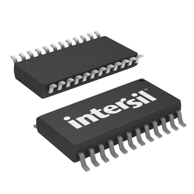
| 描述 | IC DAC 16BIT SPI/SRL 16-TSSOP数模转换器- DAC 16b 4ch SPI IF w/on-chip Ref |
| 产品分类 | |
| 品牌 | Analog Devices Inc |
| 产品手册 | |
| 产品图片 |
|
| rohs | 符合RoHS无铅 / 符合限制有害物质指令(RoHS)规范要求 |
| 产品系列 | 数据转换器IC,数模转换器- DAC,Analog Devices AD5686RBRUZnanoDAC+™ |
| 数据手册 | |
| 产品型号 | AD5686RBRUZ |
| PCN设计/规格 | |
| 产品培训模块 | http://www.digikey.cn/PTM/IndividualPTM.page?site=cn&lang=zhs&ptm=26125http://www.digikey.cn/PTM/IndividualPTM.page?site=cn&lang=zhs&ptm=26140http://www.digikey.cn/PTM/IndividualPTM.page?site=cn&lang=zhs&ptm=26150http://www.digikey.cn/PTM/IndividualPTM.page?site=cn&lang=zhs&ptm=26147 |
| 产品种类 | 数模转换器- DAC |
| 位数 | 16 |
| 供应商器件封装 | 16-TSSOP |
| 分辨率 | 16 bit |
| 包装 | 管件 |
| 商标 | Analog Devices |
| 安装类型 | 表面贴装 |
| 安装风格 | SMD/SMT |
| 封装 | Tube |
| 封装/外壳 | 16-TSSOP(0.173",4.40mm 宽) |
| 封装/箱体 | TSSOP-16 |
| 工作温度 | -40°C ~ 105°C |
| 工厂包装数量 | 96 |
| 建立时间 | 8µs |
| 接口类型 | SPI |
| 数据接口 | SPI, DSP |
| 最大工作温度 | + 105 C |
| 最小工作温度 | - 40 C |
| 标准包装 | 1 |
| 特色产品 | http://www.digikey.com/product-highlights/cn/zh/analog-devices-ad568xr-ad569xr-nanodac/1928http://www.digikey.cn/product-highlights/zh/analog-devices-ad568x-and-ad569x-nanodac/52095http://www.digikey.cn/product-highlights/cn/zh/analog-devices-select-q2-2014-products/4186 |
| 电压参考 | Internal, External |
| 电压源 | 模拟和数字 |
| 电源电压-最大 | 5.5 V |
| 电源电压-最小 | 2.7 V |
| 积分非线性 | +/- 3 LSB |
| 稳定时间 | 5 us |
| 系列 | AD5686R |
| 结构 | Resistor String |
| 转换器数 | 4 |
| 转换器数量 | 4 |
| 输出数和类型 | 4 电压 |
| 输出类型 | Voltage |
| 采样比 | 25 MSPs |
| 采样率(每秒) | - |


- 商务部:美国ITC正式对集成电路等产品启动337调查
- 曝三星4nm工艺存在良率问题 高通将骁龙8 Gen1或转产台积电
- 太阳诱电将投资9.5亿元在常州建新厂生产MLCC 预计2023年完工
- 英特尔发布欧洲新工厂建设计划 深化IDM 2.0 战略
- 台积电先进制程称霸业界 有大客户加持明年业绩稳了
- 达到5530亿美元!SIA预计今年全球半导体销售额将创下新高
- 英特尔拟将自动驾驶子公司Mobileye上市 估值或超500亿美元
- 三星加码芯片和SET,合并消费电子和移动部门,撤换高东真等 CEO
- 三星电子宣布重大人事变动 还合并消费电子和移动部门
- 海关总署:前11个月进口集成电路产品价值2.52万亿元 增长14.8%


PDF Datasheet 数据手册内容提取
Quad, 16-/14-/12-Bit nanoDAC+ with 2 ppm/°C Reference, SPI Interface Data Sheet AD5686R/AD5685R/AD5684R FEATURES FUNCTIONAL BLOCK DIAGRAM High relative accuracy (INL): ±2 LSB maximum at 16 bits Low drift 2.5 V reference: 2 ppm/°C typical VDD GND VREF Tiny package: 3 mm × 3 mm, 16-lead LFCSP Total unadjusted error (TUE): ±0.1% of FSR maximum AD5686R/AD5685R/AD5684R 2.5V REFERENCE Offset error: ±1.5 mV maximum VLOGIC Gain error: ±0.1% of FSR maximum REINGPISUTTER REGDIASCTER SDTARCIN AG VOUTA SCLK BUFFER High drive capability: 20 mA, 0.5 V from supply rails C User selectable gain of 1 or 2 (GAIN pin) SYNC LOGI REINGPISUTTER REGDIASCTER SDTARCIN BG VOUTB Reset to zero scale or midscale (RSTSEL pin) CE BUFFER A 1.8 V logic compatibility SDIN TERF REINGPISUTTER REGDIASCTER SDTARCIN CG VOUTC 50 MHz SPI with readback or daisy chain IN BUFFER SDO Low glitch: 0.5 nV-sec REINGPISUTTER REGDIASCTER SDTARCIN DG VOUTD Low power: 3.3 mW at 3 V BUFFER 2.7 V to 5.5 V power supply POWER-ON GAIN POWER- RESET ×1/×2 DOWN −40°C to +105°C temperature range LOGIC APPLICATIONS LDAC RESET RSTSEL GAIN 10485-001 Figure 1. Optical transceivers Base-station power amplifiers Process control (PLC I/O cards) Industrial automation Data acquisition systems GENERAL DESCRIPTION The AD5686R/AD5685R/AD5684R, members of the Table 1. Quad nanoDAC+ Devices nanoDAC+® family, are low power, quad, 16-/14-/12-bit Interface Reference 16-Bit 14-Bit 12-Bit buffered voltage output DACs. The devices include a 2.5 V, SPI Internal AD5686R AD5685R AD5684R 2 ppm/°C internal reference (enabled by default) and a gain External AD5686 AD5684 select pin giving a full-scale output of 2.5 V (gain = 1) or 5 V I2C Internal AD5696R AD5695R AD5694R (gain = 2). All devices operate from a single 2.7 V to 5.5 V External AD5696 AD5694 supply, are guaranteed monotonic by design, and exhibit less than 0.1% FSR gain error and 1.5 mV offset error performance. PRODUCT HIGHLIGHTS The devices are available in a 3 mm × 3 mm LFCSP and a TSSOP package. 1. High Relative Accuracy (INL). AD5686R (16-bit): ±2 LSB maximum The AD5686R/AD5685R/AD5684R also incorporate a power- AD5685R (14-bit): ±1 LSB maximum on reset circuit and a RSTSEL pin that ensures that the DAC AD5684R (12-bit): ±1 LSB maximum outputs power up to zero scale or midscale and remains there 2. Low Drift 2.5 V On-Chip Reference. until a valid write takes place. Each part contains a per-channel 2 ppm/°C typical temperature coefficient power-down feature that reduces the current consumption of 5 ppm/°C maximum temperature coefficient the device to 4 μA at 3 V while in power-down mode. 3. Two Package Options. The AD5686R/AD5685R/AD5684R employ a versatile SPI 3 mm × 3 mm, 16-lead LFCSP interface that operates at clock rates up to 50 MHz, and all 16-lead TSSOP devices contain a V pin intended for 1.8 V/3 V/5 V logic. LOGIC Rev. D Document Feedback Information furnished by Analog Devices is believed to be accurate and reliable. However, no responsibility is assumed by Analog Devices for its use, nor for any infringements of patents or other One Technology Way, P.O. Box 9106, Norwood, MA 02062-9106, U.S.A. rights of third parties that may result from its use. Specifications subject to change without notice. No license is granted by implication or otherwise under any patent or patent rights of Analog Devices. Tel: 781.329.4700 ©2012–2017 Analog Devices, Inc. All rights reserved. Trademarks and registered trademarks are the property of their respective owners. Technical Support www.analog.com
AD5686R/AD5685R/AD5684R Data Sheet TABLE OF CONTENTS Features .............................................................................................. 1 Write and Update Commands .................................................. 22 Applications ....................................................................................... 1 Daisy-Chain Operation ............................................................. 23 Functional Block Diagram .............................................................. 1 Readback Operation .................................................................. 23 General Description ......................................................................... 1 Power-Down Operation ............................................................ 24 Product Highlights ........................................................................... 1 Load DAC (Hardware LDAC Pin) ........................................... 25 Revision History ............................................................................... 2 LDAC Mask Register ................................................................. 25 Specifications ..................................................................................... 3 Hardware Reset (RESET) .......................................................... 26 AC Characteristics ........................................................................ 5 Reset Select Pin (RSTSEL) ........................................................ 26 Timing Characteristics ................................................................ 6 Internal Reference Setup ........................................................... 26 Daisy-Chain and Readback Timing Characteristics................ 7 Solder Heat Reflow ..................................................................... 26 Absolute Maximum Ratings ............................................................ 9 Thermal Hysteresis .................................................................... 27 ESD Caution .................................................................................. 9 Long-Term Temperature Drift ................................................. 27 Pin Configuration and Function Descriptions ........................... 10 Applications Information .............................................................. 28 Typical Performance Characteristics ........................................... 11 Microprocessor Interfacing ....................................................... 28 Terminology .................................................................................... 18 AD5686R/AD5685R/AD5684R to ADSP-BF531 Interface .... 28 Theory of Operation ...................................................................... 20 AD5686R/AD5685R/AD5684R to SPORT Interface ............ 28 Digital-to-Analog Converter .................................................... 20 Layout Guidelines....................................................................... 28 Transfer Function ....................................................................... 20 Galvanically Isolated Interface ................................................. 29 DAC Architecture ....................................................................... 20 Outline Dimensions ....................................................................... 30 Serial Interface ............................................................................ 21 Ordering Guide .......................................................................... 31 Standalone Operation ................................................................ 22 REVISION HISTORY 1/2017—Rev. C to Rev. D 5/2014—Rev. B to Rev. C. Changes to Features Section............................................................ 1 Deleted Long-Term Stability/Drift Parameter, Table 1 ................ 4 Changes to V Parameter, Table 2 ............................................ 4 Deleted Figure 11; Renumbered Sequentially ............................ 11 LOGIC Changes to Output Noise Spectral Density Parameter, Deleted Long-Term Temperature Drift Section and Figure 58; Table 3 ................................................................................................ 5 Renumbered Sequentially ............................................................. 26 Changes to Table 4 and Figure 2 ..................................................... 6 Changes to Table 5 and Figure 4 ..................................................... 7 6/2013—Rev. A to Rev. B Changes to Figure 5 .......................................................................... 8 Changes to Pin GAIN and Pin RSTSEL Descriptions; Table 6 ....10 Changes to Table 6 ............................................................................ 9 Changes to RESET Pin Description, Table 7............................... 10 9/2012—Rev. 0 to Rev. A Changes to Table 8 .......................................................................... 21 Changes to Table 1 ............................................................................. 1 Changes to Readback Operation Section .................................... 23 Changes to Figure 13...................................................................... 11 Changes to Hardware Reset (RESET) Section ............................ 26 Changes to Figure 36...................................................................... 15 Added Long-Term Temperature Drift Section and Figure 58 .......................................................................................... 27 4/2012—Revision 0: Initial Version Rev. D | Page 2 of 31
Data Sheet AD5686R/AD5685R/AD5684R SPECIFICATIONS V = 2.7 V to 5.5 V; 1.62 V ≤ V ≤ 5.5 V; all specifications T to T , unless otherwise noted. R = 2 kΩ; C = 200 pF. DD LOGIC MIN MAX L L Table 2. A Grade1 B Grade1 Parameter Min Typ Max Min Typ Max Unit Test Conditions/Comments STATIC PERFORMANCE2 AD5686R Resolution 16 16 Bits Relative Accuracy ±2 ±8 ±1 ±2 LSB Gain = 2 ±2 ±8 ±1 ±3 Gain = 1 Differential Nonlinearity ±1 ±1 LSB Guaranteed monotonic by design AD5685R Resolution 14 14 Bits Relative Accuracy ±0.5 ±4 ±0.5 ±1 LSB Differential Nonlinearity ±1 ±1 LSB Guaranteed monotonic by design AD5684R Resolution 12 12 Bits Relative Accuracy ±0.12 ±2 ±0.12 ±1 LSB Differential Nonlinearity ±1 ±1 LSB Guaranteed monotonic by design Zero-Code Error 0.4 4 0.4 1.5 mV All zeros loaded to DAC register Offset Error +0.1 ±4 +0.1 ±1.5 mV Full-Scale Error +0.01 ±0.2 +0.01 ±0.1 % of All ones loaded to DAC register FSR Gain Error ±0.02 ±0.2 ±0.02 ±0.1 % of FSR Total Unadjusted Error ±0.01 ±0.25 ±0.01 ±0.1 % of External reference; gain = 2; TSSOP FSR ±0.25 ±0.2 % of Internal reference; gain = 1; TSSOP FSR Offset Error Drift3 ±1 ±1 µV/°C Gain Temperature ±1 ±1 ppm Of FSR/°C Coefficient3 DC Power Supply Rejection 0.15 0.15 mV/V DAC code = midscale; VDD = 5 V ± 10% Ratio3 DC Crosstalk3 ±2 ±2 µV Due to single channel, full-scale output change ±3 ±3 µV/mA Due to load current change ±2 ±2 µV Due to powering down (per channel) OUTPUT CHARACTERISTICS3 Output Voltage Range 0 VREF 0 VREF V Gain = 1 0 2 × VREF 0 2 × VREF V Gain = 2, see Figure 33 Capacitive Load Stability 2 2 nF RL = ∞ 10 10 nF RL = 1 kΩ Resistive Load4 1 1 kΩ Load Regulation 80 80 µV/mA 5 V ± 10%, DAC code = midscale; −30 mA ≤ IOUT ≤ 30 mA 80 80 µV/mA 3 V ± 10%, DAC code = midscale; −20 mA ≤ IOUT ≤ 20 mA Short-Circuit Current5 40 40 mA Load Impedance at Rails6 25 25 Ω See Figure 33 Power-Up Time 2.5 2.5 µs Coming out of power-down mode; VDD = 5 V Rev. D | Page 3 of 31
AD5686R/AD5685R/AD5684R Data Sheet A Grade1 B Grade1 Parameter Min Typ Max Min Typ Max Unit Test Conditions/Comments REFERENCE OUTPUT Output Voltage7 2.4975 2.5025 2.4975 2.5025 V At ambient Reference TC8, 9 5 20 2 5 ppm/°C See the Terminology section Output Impedance3 0.04 0.04 Ω Output Voltage Noise3 12 12 µV p-p 0.1 Hz to 10 Hz Output Voltage Noise 240 240 nV/√Hz At ambient; f = 10 kHz, CL = 10 nF Density3 Load Regulation Sourcing3 20 20 µV/mA At ambient Load Regulation Sinking3 40 40 µV/mA At ambient Output Current Load ±5 ±5 mA VDD ≥ 3 V Capability3 Line Regulation3 100 100 µV/V At ambient Thermal Hysteresis3 125 125 ppm First cycle 25 25 ppm Additional cycles LOGIC INPUTS3 Input Current ±2 ±2 µA Per pin VINL, Input Low Voltage 0.3 × VLOGIC 0.3 × VLOGIC V VINH, Input High Voltage 0.7 × VLOGIC 0.7 × VLOGIC V Pin Capacitance 2 2 pF LOGIC OUTPUTS (SDO)3 Output Low Voltage, VOL 0.4 0.4 V ISINK = 200 μA Output High Voltage, VOH VLOGIC − 0.4 VLOGIC − 0.4 V ISOURCE = 200 μA Floating State Output 4 4 pF Capacitance POWER REQUIREMENTS VLOGIC 1.62 5.5 1.62 5.5 V ILOGIC 3 3 µA VDD 2.7 5.5 2.7 5.5 V Gain = 1 VDD VREF + 1.5 5.5 VREF + 1.5 5.5 V Gain = 2 IDD VIH = VDD, VIL = GND, VDD = 2.7 V to 5.5 V Normal Mode10 0.59 0.7 0.59 0.7 mA Internal reference off 1.1 1.3 1.1 1.3 mA Internal reference on, at full scale All Power-Down 1 4 1 4 µA −40°C to +85°C Modes11 6 6 µA −40°C to +105°C 1 Temperature range: A and B grade: −40°C to +105°C. 2 DC specifications tested with the outputs unloaded, unless otherwise noted. Upper dead band = 10 mV and exists only when VREF = VDD with gain = 1 or when VREF/2 = VDD with gain = 2. Linearity calculated using a reduced code range of 256 to 65,280 (AD5686R), 64 to 16,320 (AD5685R), and 12 to 4080 (AD5684R). 3 Guaranteed by design and characterization; not production tested. 4 Channel A and Channel B can have a combined output current of up to 30 mA. Similarly, Channel C and Channel D can have a combined output current of up to 30 mA up to a junction temperature of 110°C. 5 VDD = 5 V. The device includes current limiting that is intended to protect the device during temporary overload conditions. Junction temperature can be exceeded during current limit. Operation above the specified maximum operation junction temperature may impair device reliability. 6 When drawing a load current at either rail, the output voltage headroom with respect to that rail is limited by the 25 Ω typical channel resistance of the output devices. For example, when sinking 1 mA, the minimum output voltage = 25 Ω × 1 mA = 25 mV (see Figure 33). 7 Initial accuracy presolder reflow is ±750 µV; output voltage includes the effects of preconditioning drift. See the Internal Reference Setup section. 8 Reference is trimmed and tested at two temperatures and is characterized from −40°C to +105°C. 9 Reference temperature coefficient calculated as per the box method. See the Terminology section for further information. 10 Interface inactive. All DACs active. DAC outputs unloaded. 11 All DACs powered down. Rev. D | Page 4 of 31
Data Sheet AD5686R/AD5685R/AD5684R AC CHARACTERISTICS V = 2.7 V to 5.5 V; R = 2 kΩ to GND; C = 200 pF to GND; 1.62 V ≤ V ≤ 5.5 V; all specifications T to T , unless otherwise DD L L LOGIC MIN MAX noted.1 Table 3. Parameter2 Min Typ Max Unit Test Conditions/Comments3 Output Voltage Settling Time AD5686R 5 8 µs ¼ to ¾ scale settling to ±2 LSB AD5685R 5 8 µs ¼ to ¾ scale settling to ±2 LSB AD5684R 5 7 µs ¼ to ¾ scale settling to ±2 LSB Slew Rate 0.8 V/µs Digital-to-Analog Glitch Impulse 0.5 nV-sec 1 LSB change around major carry Digital Feedthrough 0.13 nV-sec Digital Crosstalk 0.1 nV-sec Analog Crosstalk 0.2 nV-sec DAC-to-DAC Crosstalk 0.3 nV-sec Total Harmonic Distortion4 −80 dB At ambient, BW = 20 kHz, V = 5 V, f = 1 kHz DD OUT Output Noise Spectral Density 300 nV/√Hz DAC code = midscale, 10 kHz; gain = 2, internal reference enable Output Noise 6 µV p-p 0.1 Hz to 10 Hz SNR 90 dB At ambient, BW = 20 kHz, V = 5 V, f = 1 kHz DD OUT SFDR 83 dB At ambient, BW = 20 kHz, V = 5 V, f = 1 kHz DD OUT SINAD 80 dB At ambient, BW = 20 kHz, V = 5 V, f = 1 kHz DD OUT 1 Guaranteed by design and characterization, not production tested. 2 See the Terminology section. 3 Temperature range is −40°C to +105°C, typical at 25°C. 4 Digitally generated sine wave at 1 kHz. Rev. D | Page 5 of 31
AD5686R/AD5685R/AD5684R Data Sheet TIMING CHARACTERISTICS All input signals are specified with t = t = 1 ns/V (10% to 90% of V ) and timed from a voltage level of (V + V )/2. See Figure 2. R F DD IL IH V = 2.7 V to 5.5 V, 1.62 V ≤ V ≤ 5.5 V; V = 2.5 V. All specifications T to T , unless otherwise noted. DD LOGIC REFIN MIN MAX Table 4. 1.62 V ≤ V < 2.7 V 2.7 V ≤ V ≤ 5.5 V LOGIC LOGIC Parameter1 Symbol Min Max Min Max Unit SCLK Cycle Time t 20 20 ns 1 SCLK High Time t 10 10 ns 2 SCLK Low Time t 10 10 ns 3 SYNCE to SCLK Falling Edge Setup Time t4 15 10 ns Data Setup Time t 5 5 ns 5 Data Hold Time t 5 5 ns 6 SCLK Falling Edge to SYNCE Rising Edge t7 10 10 ns Minimum SYNCE High Time t8 20 20 ns SYNCE Rising Edge to SYNCE Rising Edge (DAC Register Updates) t9 870 830 ns SYNCE Falling Edge to SCLK Fall Ignore t10 16 10 ns LDACE Pulse Width Low t11 15 15 ns SYNCE Rising Edge to LDACE Rising Edge t12 20 20 ns SYNCE Rising Edge to LDACE Falling Edge t13 30 30 ns LDACE Falling Edge to SYNCE Rising Edge t14 840 800 ns Minimum Pulse Width Low t 30 30 ns 15 Pulse Activation Time t 30 30 ns 16 Power-Up Time2 4.5 4.5 μs 1Guaranteed by design and characterization; not production tested. 2 Time to exit power-down to normal mode of AD5686R/AD5685R/AD5684R operation, SYNCE rising edge to 90% of DAC midscale value, with output unloaded. t10 t1 SCLK t8 t3 t2 t7 t14 t 4 SYNC t 9 t 6 t 5 SDIN DB23 DB0 t t 11 13 LDAC1 t 12 LDAC2 t RESET 15 VOUT t16 12ASYSNYNCCHHRROONNOOUUS SL DLDAACC U UPDPDAATET EM MOODDE.E. 10485-002 Figure 2. Serial Write Operation Rev. D | Page 6 of 31
Data Sheet AD5686R/AD5685R/AD5684R DAISY-CHAIN AND READBACK TIMING CHARACTERISTICS 17B All input signals are specified with t = t = 1 ns/V (10% to 90% of V ) and timed from a voltage level of (V + V )/2. See Figure 4 R F DD IL IH and Figure 5. V = 2.7 V to 5.5 V, 1.62 V ≤ V ≤ 5.5 V; V = 2.5 V. All specifications T to T , unless otherwise noted. V = DD LOGIC REF MIN MAX DD 2.7 V to 5.5 V. Table 5. 1.62 V ≤ V < 2.7 V 2.7 V ≤ V ≤ 5.5 V LOGIC LOGIC Parameter1 Symbol Min Max Min Max Unit 17F SCLK Cycle Time t 66 40 ns 1 SCLK High Time t 33 20 ns 2 SCLK Low Time t 33 20 ns 3 ASYNCEEA to SCLK Falling Edge t4 33 20 ns Data Setup Time t 5 5 ns 5 Data Hold Time t 5 5 ns 6 SCLK Falling Edge to ASYNCEEA Rising Edge t7 15 10 ns Minimum ASYNCEEA High Time t8 60 30 ns SDO Data Valid from SCLK Rising Edge t 45 30 ns 9 ASYNCEEA Rising Edge to SCLK Falling Edge t10 15 10 ns ASYNCEEA Rising Edge to SDO Disable t11 60 60 ns 1 Guaranteed by design and characterization; not production tested. Circuit and Timing Diagrams 42B 200µA IOL TO OUTPPUINT VOH (MIN) CL 20pF 200µA IOH 10485-003 Figure 3. Load Circuit for Digital Output (SDO) Timing Specifications t1 24 48 t8 t2 t7 t4 t3 t10 t6 t5 DB23 DB0 DB23 DB0 INPUT WORD FOR DAC N INPUT WORD FOR DAC N + 1 t9 UNDEFINED INPUT WORD FOR DAC N 10485-004 Figure 4. Daisy-Chain Timing Diagram Rev. D | Page 7 of 31
AD5686R/AD5685R/AD5684R Data Sheet t1 SCLK 1 24 1 24 t8 t4 t3 t2 t7 t8 t10 SYNC t6 t5 SDIN DB23 DB0 DB23 DB0 INPUT WORD SPECIFIES NOP CONDITION REGISTER TO BE READ t9 t11 SDO DB23 DB0 HI-Z SELECCTLEOD CRKEEGDIS OTUETR DATA 10485-005 Figure 5. Readback Timing Diagram Rev. D | Page 8 of 31
Data Sheet AD5686R/AD5685R/AD5684R ABSOLUTE MAXIMUM RATINGS T = 25°C, unless otherwise noted. A Stresses at or above those listed under Absolute Maximum Ratings may cause permanent damage to the product. This is a Table 6. stress rating only; functional operation of the product at these Parameter Rating or any other conditions above those indicated in the operational V to GND −0.3 V to +7 V DD section of this specification is not implied. Operation beyond V to GND −0.3 V to +7 V LOGIC the maximum operating conditions for extended periods may V to GND −0.3 V to V + 0.3 V OUT DD affect product reliability. V to GND −0.3 V to V + 0.3 V REF DD Digital Input Voltage to GND −0.3 V to V + 0.3 V LOGIC ESD CAUTION Operating Temperature Range −40°C to +105°C Storage Temperature Range −65°C to +150°C Junction Temperature 125°C 16-Lead TSSOP, θ Thermal 112.6°C/W JA Impedance, 0 Airflow (4-Layer Board) 16-Lead LFCSP, θJA Thermal 70°C/W Impedance, 0 Airflow (4-Layer Board) Reflow Soldering Peak 260°C Temperature, Pb Free (J-STD-020) Rev. D | Page 9 of 31
AD5686R/AD5685R/AD5684R Data Sheet PIN CONFIGURATION AND FUNCTION DESCRIPTIONS 2B AD5686R/AD5685R/AD5684R L BTUO FER ESTS TESE V V R R 6 5 4 3 1 1 1 1 VOUTA1 12SDIN GND2 11SYNC VREF 1 16 RSTSEL VDD3 10SCLK VOUTB 2 15 RESET VOUTC4 9 VLOGIC AD5686R/ VOUTA 3 AD5685R/ 14 SDIN 5 6 7 8 GND 4 AD5684R 13 SYNC DVTUO ODS CADL NIAG VOVUTDCD 56 (NToOt Pto V SIEcaWle) 1121 SVCLOLGKIC TOP VIEW (Not to Scale) VOUTD 7 10 GAIN N1.O TTHEES EXPOSED PAD MUST BE TIED TO GND. 10485-006 SDO 8 9 LDAC 10485-007 Figure 6. 16-Lead LFCSP Pin Configuration Figure 7. 16-Lead TSSOP Pin Configuration Table 7. Pin Function Descriptions Pin No. LFCSP TSSOP Mnemonic Description 1 3 V A Analog Output Voltage from DAC A. The output amplifier has rail-to-rail operation. OUT 2 4 GND Ground Reference Point for All Circuitry on the Part. 3 5 V Power Supply Input. These parts can be operated from 2.7 V to 5.5 V, and the supply should be DD decoupled with a 10 µF capacitor in parallel with a 0.1 µF capacitor to GND. 4 6 V C Analog Output Voltage from DAC C. The output amplifier has rail-to-rail operation. OUT 5 7 V D Analog Output Voltage from DAC D. The output amplifier has rail-to-rail operation. OUT 6 8 SDO Serial Data Output. Can be used to daisy-chain a number of AD5686R/AD5685R/AD5684R devices together or can be used for readback. The serial data is transferred on the rising edge of SCLK and is valid on the falling edge of the clock. 7 9 LDACE LDACE can be operated in two modes, asynchronously and synchronously. Pulsing this pin low allows A A A any or all DAC registers to be updated if the input registers have new data. This allows all DAC outputs to simultaneously update. This pin can also be tied permanently low. 8 10 GAIN Span Set Pin. When this pin is tied to GND, all four DAC outputs have a span from 0 V to V . If this REF pin is tied to V , all four DACs output a span of 0 V to 2 × V . LOGIC REF 9 11 V Digital Power Supply. Voltage ranges from 1.8 V to 5.5 V. LOGIC 10 12 SCLK Serial Clock Input. Data is clocked into the input shift register on the falling edge of the serial clock input. Data can be transferred at rates of up to 50 MHz. 11 13 SYNCE Active Low Control Input. This is the frame synchronization signal for the input data. When SYNCE A A A goes low, data is transferred in on the falling edges of the next 24 clocks. 12 14 SDIN Serial Data Input. This device has a 24-bit input shift register. Data is clocked into the register on the falling edge of the serial clock input. 13 15 RESETE Asynchronous Reset Input. The RESETE input is falling edge sensitive. When RESETE is low, all LDACE A A A A A A A pulses are ignored. When RESETE is activated, the input register and the DAC register are updated A A with zero scale or midscale, depending on the state of the RSTSEL pin. If the pin is forced low at power-up, the POR circuit does not initialize correctly until the pin is released. 14 16 RSTSEL Power-On Reset Pin. Tying this pin to GND powers up all four DACs to zero scale. Tying this pin to V powers up all four DACs to midscale. LOGIC 15 1 V Reference Voltage. The AD5686R/AD5685R/AD5684R have a common reference pin. When using REF the internal reference, this is the reference output pin. When using an external reference, this is the reference input pin. The default for this pin is as a reference output. 16 2 V B Analog Output Voltage from DAC B. The output amplifier has rail-to-rail operation. OUT 17 N/A EPAD Exposed Pad. The exposed pad must be tied to GND. Rev. D | Page 10 of 31
Data Sheet AD5686R/AD5685R/AD5684R TYPICAL PERFORMANCE CHARACTERISTICS 3B 2.5020 DDEEVVIICCEE 12 VDD = 5V 1600 VTAD D= =2 55°VC 2.5015 DEVICE 3 1400 DEVICE 4 2.5010 DEVICE 5 1200 2.5005 Hz) 1000 V (V)REF 2.5000 SD (nV/ 800 2.4995 N 600 2.4990 400 2.4985 200 2.4980–40 –20 0 T2E0MPER4A0TURE6 (0°C) 80 100 120 10485-212 010 100 FR1EkQUENCY (1M0Hkz) 100k 1M 10485-111 Figure 8. Internal Reference Voltage vs. Temperature (Grade B) Figure 11. Internal Reference Noise Spectral Density vs. Frequency 2.5020 DEVICE 1 DEVICE 2 VDD = 5V T 2.5015 DEVICE 3 TA = 25°C DEVICE 4 2.5010 DEVICE 5 2.5005 V) (REF 2.5000 1 V 2.4995 2.4990 2.4985 VDD = 5V 2.4980–40 –20 0 T2E0MPER4A0TURE6 (0°C) 80 100 120 10485-109 CH1 2µV M1.0s A CH1 160mV 10485-112 Figure 9. Internal Reference Voltage vs. Temperature (Grade A) Figure 12. Internal Reference Noise, 0.1 Hz to 10 Hz 90 2.5000 VDD = 5V VDD = 5V 80 TA = 25°C 2.4999 70 2.4998 TS 60 NI R OF U 50 (V)REF2.4997 E 40 V2.4996 B M NU 30 2.4995 20 2.4994 10 00 0.5 1.0 TE1M.5PER2A.0TURE2. 5DRIF3T.0 (ppm3./5°C) 4.0 4.5 5.0 10485-250 2.499–30.005 –0.003 –0.00I1LOAD (A0).001 0.003 0.005 10485-113 Figure 10. Reference Output Temperature Drift Histogram Figure 13. Internal Reference Voltage vs. Load Current Rev. D | Page 11 of 31
AD5686R/AD5685R/AD5684R Data Sheet 2.5002 TA = 25°C 10 D1 8 2.5000 6 2.4998 4 V (V)REF2.4996 D3 L (LSB) 02 N I –2 2.4994 –4 2.4992 –6 D2 –8 VDD = 5V TA = 25°C 2.4990 INTERNAL REFERENCE = 2.5V 2.5 3.0 3.5 V4.D0D (V) 4.5 5.0 5.5 10485-117 –100 625 1250 18C75ODE 2500 3125 3750 4096 10485-120 Figure 14. Internal Reference Voltage vs. Supply Voltage Figure 17. AD5684R INL 10 1.0 8 0.8 6 0.6 4 0.4 B) 2 B) 0.2 NL (LS 0 NL (LS 0 I –2 D–0.2 –4 –0.4 –6 –0.6 –8 VDD = 5V –0.8 VDD = 5V TA = 25°C TA = 25°C INTERNAL REFERENCE = 2.5V INTERNAL REFERENCE = 2.5V –100 10000 20000 300C0O0DE40000 50000 60000 10485-118 –1.00 10000 20000 300C0O0DE40000 50000 60000 10485-121 Figure 15. AD5686R INL Figure 18. AD5686R DNL 10 1.0 8 0.8 6 0.6 4 0.4 B) 2 B) 0.2 S S NL (L 0 NL (L 0 I –2 D–0.2 –4 –0.4 –6 –0.6 –8 TVAD D= =2 55°VC –0.8 TVAD D= =2 55°VC INTERNAL REFERENCE = 2.5V INTERNAL REFERENCE = 2.5V –100 2500 5000 75C00ODE10000 12500 1500016348 10485-119 –1.00 2500 5000 75C00ODE10000 12500 1500016383 10485-122 Figure 16. AD5685R INL Figure 19. AD5685R DNL Rev. D | Page 12 of 31
Data Sheet AD5686R/AD5685R/AD5684R 1.0 10 0.8 8 0.6 6 0.4 4 B) 0.2 SB) 2 NL (LS 0 ROR (L 0 DINNLL D –0.2 R –2 E –0.4 –4 –0.6 –6 –0.8 TVAD D= =2 55°VC –8 ITNAT =E R25N°ACL REFERENCE = 2.5V INTERNAL REFERENCE = 2.5V –1.0 –10 0 625 1250 18C75ODE 2500 3125 3750 4096 10485-123 2.7 3.2 S3U.7PPLY VOL4.T2AGE (V)4.7 5.2 12975-126 Figure 20. AD5684R DNL Figure 23. INL Error and DNL Error vs. Supply Voltage 10 0.10 8 0.08 6 0.06 4 0.04 R) R (LSB) 02 INL % of FS 0.020 FULL-SCALE ERROR RO DNL R ( GAIN ERROR ER –2 RO–0.02 R –4 E–0.04 –6 –0.06 –8 VDD = 5V –0.08 VDD = 5V INTERNAL REFERENCE = 2.5V INTERNAL REFERENCE = 2.5V –10–40 10 TEMPERATURE6 (0°C) 110 12975-124 –0.10–40 –20 0 T2E0MPER4A0TURE6 (0°C) 80 100 120 12975-127 Figure 21. INL Error and DNL Error vs. Temperature Figure 24. Gain Error and Full-Scale Error vs. Temperature 10 1.4 IVNDTDE =R N5VAL REFERENCE = 2.5V 8 1.2 6 4 1.0 R (LSB) 02 INL OR (mV) 0.8 O DNL R R R 0.6 R –2 E E –4 0.4 ZERO-CODE ERROR –6 VDD = 5V TA = 25°C 0.2 –8 OFFSET ERROR 0 –100 0.5 1.0 1.5 2.0VR2E.F5 (V)3.0 3.5 4.0 4.5 5.0 12975-125 Fig–u40re 25–. 2Z0ero-C0ode ErT2rEo0Mr aPnERd4A 0OTfUfsReEt6 E(0°rCr)or v8s0. Tem1p0e0ratu1r2e0 12975-128 Figure 22. INL Error and DNL Error vs. VREF Rev. D | Page 13 of 31
AD5686R/AD5685R/AD5684R Data Sheet 0.10 0.10 0.08 R) 0.08 S 0.06 of F 0.06 % 0.04 R ( 0.04 R) O S R 0.02 F 0.02 R % of 0 GAIN ERROR ED E 0 R ( ST RO–0.02 FULL-SCALE ERROR JU–0.02 R D E–0.04 NA–0.04 U –0.06 AL –0.06 T –0.08 TA = 25°C TO–0.08 VTAD D= =2 55°VC INTERNAL REFERENCE = 2.5V INTERNAL REFERENCE = 2.5V –0.102.7 3.2 S3U.7PPLY VO4L.T2AGE (V)4.7 5.2 12975-129 –0.102.7 3.2 S3U.7PPLY VO4L.T2AGE (V)4.7 5.2 10485-132 Figure 26. Gain Error and Full-Scale Error vs. Supply Figure 29. TUE vs. Supply, Gain = 1 1.5 0 1.0 R)–0.01 S of F–0.02 % V) 0.5 ZERO-CODE ERROR OR (–0.03 m R–0.04 R ( 0 ER ERRO OFFSET ERROR STED –0.05 –0.5 JU–0.06 D NA–0.07 U –1.0 AL –0.08 –1.52F.7iTIgNAuT =rEe R2 25N°7AC.3L Z.2 RerEoF-ECRoEdSN3eUC. 7PEErP r=Lo Y2r. a5VVnOd4L.T 2OAfGfsEe t(V E)r4r.o7r vs. Sup5p.2ly 12975-130 TOT––00..01900TIVNADT D=E =R2 15N50°VAC0L00 REFE20R0E0N0CE =3 020C.50OV0DE 40000 50000 6000065535 10485-133 Figure 30. TUE vs. Code 0.10 VDD = 5V % of FSR) 00..0098 INTERNAL REFERENCE = 2.5V 25 VTERAXDE DTF= EE =2RR 55NE°VCANLCE = 2.5V R ( 0.07 20 O R 0.06 R E ED 0.05 S 15 UST 0.04 HIT J NAD 0.03 10 U AL 0.02 OT 5 T 0.01 0–40 –20 0 T2E0MPER4A0TURE6 (0°C) 80 100 120 12975-131 0 540 560 580IDD (µA)600 620 640 12975-135 Figure 28. TUE vs. Temperature Figure 31. IDD Histogram with External Reference, 5 V Rev. D | Page 14 of 31
Data Sheet AD5686R/AD5685R/AD5684R 5 30 IVTNADT D=E =R2 5N5°VACL 4 VTGADA DI=N =2 =53 °V1C REFERENCE = 2.5V EXTERNAL 25 REFERENCE = 2.5V 3 0xFFFF 20 V) 2 0xC000 TS (UT 0x8000 HI 15 VO 1 0x4000 10 0 0x0000 5 –1 01000 1020 1040 106ID0D (µA10)80 1100 1120 1140 12975-136 –2–60 –40 –20 IOUT0 (mA) 20 40 60 12975-139 Figure 32. IDD Histogram with Internal Reference, VREFOUT = 2.5 V, Gain = 2 Figure 35. Source and Sink Capability at 3 V 1.0 1.4 0.8 0.6 1.2 FULL-SCALE 0.4 SINKING 2.7V 1.0 ZERO CODE V (V)OUT 0.02 SINKING 5V RENT (mA) 0.8 EXTERNAL REFERENCE, FULL-SCALE ∆ –0.2 UR 0.6 C –0.4 SOURCING 5V 0.4 –0.6 SOURCING 2.7V 0.2 –0.8 –1.0 0 0 5 1L0OAD CUR1R5ENT (mA2)0 25 30 10485-200 –40 10 TEMPERATURE6 (0°C) 110 10485-140 Figure 33. Headroom/Footroom vs. Load Current Figure 36. Supply Current vs. Temperature 7 6 TVGADA DI=N =2 =55 °V2C 43..05 DDAACC AB INTERNAL 0xFFFF DAC C 5 REFERENCE = 2.5V DAC D 3.0 4 0xC000 2.5 (V)OUT 23 0x8000 (V)UT 2.0 V O 0x4000 V 1 1.5 0x0000 0 1.0 –1 0.5 VTAD D= =2 55°VC INTERNAL REFERENCE = 2.5V –2 ¼ TO ¾ SCALE –0.06 Fi–g0u.0re4 34. S–o0u.0Lr2cOeA aDn CdU S0RinRkE NCTa p(Aa0).b02ility at 50 .V04 0.06 10485-138 010 20 40TIME (µs)80 160 320 10485-141 Figure 37. Settling Time, 5.25 V Rev. D | Page 15 of 31
AD5686R/AD5685R/AD5684R Data Sheet 0.06 CH A 6 0.003 CH B CH B 0.05 CH C 5 CH C CH D CH D VDD 0.002 0.04 4 V) D ( V (V)OUT 00..0023 23 V (V)DD C-COUPLE 0.001 A 0 UT 0.01 1 O V –0.001 0 0 TA = 25°C INTERNAL REFERENCE = 2.5V –0.01–10 –5 0TIME (µs)5 10 15–1 10485-142 –0.0020 5 10TIME (µs)15 20 25 10485-145 Figure 38. Power-On Reset to 0 V Figure 41. Analog Crosstalk, Channel A 3 CH A CH B CH C GAIN = 2 T CH D SYNC 2 V) (UT GAIN = 1 VO 1 1 VDD = 5V TA = 25°C VDD = 5V INTERNAL REFERENCE = 2.5V TA = 25°C 0–5 0 TIME (µs) 5 10 10485-143 CEHX1 T2EµRVNAL REFERENCE = 2.5MV1.0s A CH1 802mV 12975-146 Figure 39. Exiting Power-Down to Midscale Figure 42. 0.1 Hz to 10 Hz Output Noise Plot, External Reference 2.5008 T 2.5003 V) (UT 2.4998 O 1 V CHANNEL B 2.4993 TA = 25°C VDD = 5.25V INTERNAL REFERENCE CODE = 7FFF TO 8000 VDD = 5V ENERGY = 0.227206nV-sec TA = 25°C 2.49880 2 4 TIME6 (µs) 8 10 12 10485-144 CIHN1T E 2RµNVAL REFERENCE = 2.5VM1.0s A CH1 802mV 12975-147 Figure 40. Digital-to-Analog Glitch Impulse Figure 43. 0.1 Hz to 10 Hz Output Noise Plot, 2.5 V Internal Reference Rev. D | Page 16 of 31
Data Sheet AD5686R/AD5685R/AD5684R 4.0 11460000 TIVNADT D=E =R2 5N5°VACL REFERENCE = 2.5V FMZUEIDRLSLOC--SSACCLAAELLEE 3.9 0010n.0.12nFn2FnFF TIVNADT D=E =R2 5N5°VACL REFERENCE = 2.5V 3.8 4.7nF 1200 3.7 Hz) 1000 V) 3.6 SD (nV/ 800 V (OUT 33..45 N 600 3.3 400 3.2 200 3.1 010 100 FR1kEQUENCY 1(H0kz) 100k 1M 10485-148 3.10.590 1.595 1.600 1.605TIM1.E6 1(m0s)1.615 1.620 1.625 1.630 10485-150 Figure 44. Noise Spectral Density Figure 46. Settling Time vs. Capacitive Load 0 20 VDD = 5V 0 TA = 25°C INTERNAL REFERENCE = 2.5V –10 –20 –40 B) –20 d THD (dBV) –1––086000 ANDWIDTH ( –30 B –40 –120 –140 –50 VDD = 5V –160 TA = 25°C EXTERNAL REFERENCE = 2.5V, ±0.1V p-p –1800 2000 4000 6000 F8R00E0QU10E0N0C0Y1 2(H00z0)14000160001800020000 10485-149 –6010k 100kFREQUENCY (Hz)1M 10M 10485-151 Figure 47. Multiplying Bandwidth, External Reference = 2.5 V, ±0.1 V p-p, Figure 45. Total Harmonic Distortion at 1 kHz 10 kHz to 10 MHz Rev. D | Page 17 of 31
AD5686R/AD5685R/AD5684R Data Sheet TERMINOLOGY 4B Relative Accuracy or Integral Nonlinearity (INL) Output Voltage Settling Time For the DAC, relative accuracy or integral nonlinearity is a This is the amount of time it takes for the output of a DAC to measurement of the maximum deviation, in LSBs, from a settle to a specified level for a ¼ to ¾ full-scale input change straight line passing through the endpoints of the DAC transfer and is measured from the rising edge of SYNC. function. A typical INL vs. code plot is shown in Figure 15. Digital-to-Analog Glitch Impulse Differential Nonlinearity (DNL) Digital-to-analog glitch impulse is the impulse injected into the Differential nonlinearity is the difference between the measured analog output when the input code in the DAC register changes change and the ideal 1 LSB change between any two adjacent state. It is normally specified as the area of the glitch in nV-sec, codes. A specified differential nonlinearity of ±1 LSB maximum and is measured when the digital input code is changed by ensures monotonicity. This DAC is guaranteed monotonic by 1 LSB at the major carry transition (0x7FFF to 0x8000) (see design. A typical DNL vs. code plot can be seen in Figure 18. Figure 40). Zero-Code Error Digital Feedthrough Zero-code error is a measurement of the output error when Digital feedthrough is a measure of the impulse injected into the zero code (0x0000) is loaded to the DAC register. Ideally, the analog output of the DAC from the digital inputs of the DAC, output should be 0 V. The zero-code error is always positive in but is measured when the DAC output is not updated. It is the AD5686R because the output of the DAC cannot go below specified in nV-sec, and measured with a full-scale code change 0 V due to a combination of the offset errors in the DAC and on the data bus, that is, from all 0s to all 1s and vice versa. the output amplifier. Zero-code error is expressed in mV. A plot Reference Feedthrough of zero-code error vs. temperature can be seen in Figure 25. Reference feedthrough is the ratio of the amplitude of the signal Full-Scale Error at the DAC output to the reference input when the DAC output Full-scale error is a measurement of the output error when full- is not being updated. It is expressed in dB. scale code (0xFFFF) is loaded to the DAC register. Ideally, the Noise Spectral Density output should be V − 1 LSB. Full-scale error is expressed in DD This is a measurement of the internally generated random percent of full-scale range (% of FSR). A plot of full-scale error noise. Random noise is characterized as a spectral density vs. temperature can be seen in Figure 24. (nV/√Hz). It is measured by loading the DAC to midscale and Gain Error measuring noise at the output. It is measured in nV/√Hz. A plot This is a measure of the span error of the DAC. It is the deviation of noise spectral density is shown in Figure 44. in slope of the DAC transfer characteristic from the ideal DC Crosstalk expressed as % of FSR. DC crosstalk is the dc change in the output level of one DAC in Offset Error Drift response to a change in the output of another DAC. It is This is a measurement of the change in offset error with a measured with a full-scale output change on one DAC (or soft change in temperature. It is expressed in µV/°C. power-down and power-up) while monitoring another DAC kept at midscale. It is expressed in μV. Gain Temperature Coefficient This is a measurement of the change in gain error with changes DC crosstalk due to load current change is a measure of the in temperature. It is expressed in ppm of FSR/°C. impact that a change in load current on one DAC has to another DAC kept at midscale. It is expressed in μV/mA. Offset Error Offset error is a measure of the difference between V (actual) Digital Crosstalk OUT and V (ideal) expressed in mV in the linear region of the This is the glitch impulse transferred to the output of one DAC OUT transfer function. Offset error is measured on the AD5686R at midscale in response to a full-scale code change (all 0s to all with Code 512 loaded in the DAC register. It can be negative 1s and vice versa) in the input register of another DAC. It is or positive. measured in standalone mode and is expressed in nV-sec. DC Power Supply Rejection Ratio (PSRR) This indicates how the output of the DAC is affected by changes in the supply voltage. PSRR is the ratio of the change in V to OUT a change in V for full-scale output of the DAC. It is measured DD in mV/V. V is held at 2 V, and V is varied by ±10%. REF DD Rev. D | Page 18 of 31
Data Sheet AD5686R/AD5685R/AD5684R Analog Crosstalk Total Harmonic Distortion (THD) This is the glitch impulse transferred to the output of one DAC This is the difference between an ideal sine wave and its due to a change in the output of another DAC. It is measured by attenuated version using the DAC. The sine wave is used as the loading one of the input registers with a full-scale code change reference for the DAC, and the THD is a measurement of the (all 0s to all 1s and vice versa). Then execute a software LDAC harmonics present on the DAC output. It is measured in dB. and monitor the output of the DAC whose digital code was not Voltage Reference TC changed. The area of the glitch is expressed in nV-sec. Voltage reference TC is a measure of the change in the reference DAC-to-DAC Crosstalk output voltage with a change in temperature. The reference TC This is the glitch impulse transferred to the output of one DAC is calculated using the box method, which defines the TC as the due to a digital code change and subsequent analog output maximum change in the reference output over a given tempera- change of another DAC. It is measured by loading the attack ture range expressed in ppm/°C, as follows; channel with a full-scale code change (all 0s to all 1s and vice V −V versa), using the write to and update commands while monitor- TC= REFmax REFmin ×106 ing the output of the victim channel that is at midscale. The VREFnom×TempRange energy of the glitch is expressed in nV-sec. where: Multiplying Bandwidth V is the maximum reference output measured over the REFmax The amplifiers within the DAC have a finite bandwidth. The total temperature range. multiplying bandwidth is a measure of this. A sine wave on the V is the minimum reference output measured over the total REFmin reference (with full-scale code loaded to the DAC) appears on temperature range. the output. The multiplying bandwidth is the frequency at V is the nominal reference output voltage, 2.5 V. REFnom which the output amplitude falls to 3 dB below the input. TempRange is the specified temperature range of −40°C to +105°C. Rev. D | Page 19 of 31
AD5686R/AD5685R/AD5684R Data Sheet THEORY OF OPERATION 5B DIGITAL-TO-ANALOG CONVERTER VREF 19B The AD5686R/AD5685R/AD5684R are quad 16-/14-/12-bit, R serial input, voltage output DACs with an internal reference. The parts operate from supply voltages of 2.7 V to 5.5 V. Data is R written to the AD5686R/AD5685R/AD5684R in a 24-bit word format via a 3-wire serial interface. The AD5686R/AD5685R/ R TO OUTPUT AD5684R incorporate a power-on reset circuit to ensure that the AMPLIFIER DAC output powers up to a known output state. The devices also have a software power-down mode that reduces the typical current consumption to typically 4 µA. TRANSFER FUNCTION 20B R The internal reference is on by default. To use an external reference, only a nonreference option is available. Because the R ivnopltuatg ceo wdhinegn tuos tinhge DanA eCx tiesr sntaral irgehfet rbeinncaer yis, tghivee ind ebayl output 10485-053 D Figure 49. Resistor String Structure VOUT =VREF×Gain2N Internal Reference 43B where: The AD5686R/AD5685R/AD5684R on-chip reference is on at D is the decimal equivalent of the binary code that is loaded to power-up but can be disabled via a write to a control register. the DAC register as follows: See the Internal Reference Setup section for details. 0 to 4,095 for the 12-bit device. The AD5686R/AD5685R/AD5684R have a 2.5 V, 2 ppm/°C 0 to 16,383 for the 14-bit device. reference, giving a full-scale output of 2.5 V or 5 V, depending 0 to 65,535 for the 16-bit device. on the state of the GAIN pin. The internal reference associated N is the DAC resolution. with the device is available at the V pin. This buffered REF Gain is the gain of the output amplifier and is set to 1 by default. reference is capable of driving external loads of up to 10 mA. This can be set to ×1 or ×2 using the gain select pin. When this Output Amplifiers pin is tied to GND, all four DAC outputs have a span from 0 V 44B to V . If this pin is tied to V , all four DACs output a span of The output buffer amplifier can generate rail-to-rail voltages on REF DD 0 V to 2 × VREF. its output, which gives an output range of 0 V to VDD. The actual range depends on the value of V , the GAIN pin, offset error, DAC ARCHITECTURE REF 21B and gain error. The GAIN pin selects the gain of the output. The DAC architecture consists of a string DAC followed by an • If this pin is tied to GND, all four outputs have a gain of 1 output amplifier. Figure 48 shows a block diagram of the DAC and the output range is 0 V to V . REF architecture. • If this pin is tied to V , all four outputs have a gain of 2 LOGIC VREF and the output range is 0 V to 2 × V . REF 2.5V REF These amplifiers are capable of driving a load of 1 kΩ in parallel REF (+) with 2 nF to GND. The slew rate is 0.8 V/µs with a ¼ to ¾ scale REINGPISUTTER REGDIASCTER RSETSRISINTOGR VOUTX settling time of 5 µs. REF (–) GND (GAING =A I1N OR 2) 10485-052 Figure 48. Single DAC Channel Architecture Block Diagram The resistor string structure is shown in Figure 49. It is a string of resistors, each of Value R. The code loaded to the DAC register determines the node on the string where the voltage is to be tapped off and fed into the output amplifier. The voltage is tapped off by closing one of the switches connecting the string to the amplifier. Because it is a string of resistors, it is guaranteed monotonic. Rev. D | Page 20 of 31
Data Sheet AD5686R/AD5685R/AD5684R SERIAL INTERFACE Table 8. Command Definitions 22B Command The AD5686R/AD5685R/AD5684R have a 3-wire serial C3 C2 C1 C0 Description interface (SYNCE, SCLK, and SDIN) that is compatible with A A 0 0 0 0 No operation SPI, QSPI, and MICROWIRE interface standards as well as 0 0 0 1 Write to Input Register n (dependent on LDACE) most DSPs. See Figure 2 for a timing diagram of a typical A A 0 0 1 0 Update DAC Register n with contents of Input write sequence. The AD5686R/AD5685R/AD5684R contain Register n an SDO pin to allow the user to daisy-chain multiple devices 0 0 1 1 Write to and update DAC Channel n together (see the Daisy-Chain Operation section) or for 0 1 0 0 Power down/power up DAC readback. 0 1 0 1 Hardware LDACE mask register A A 0 1 1 0 Software reset (power-on reset) Input Shift Register 45B 0 1 1 1 Internal reference setup register The input shift register of the AD5686R/AD5685R/AD5684R is 1 0 0 0 Set up DCEN register (daisy-chain enable) 24 bits wide. Data is loaded MSB first (DB23) and the first four 1 0 0 1 Set up readback register (readback enable) bits are the command bits, C3 to C0 (see Table 8), followed by 1 0 1 0 Reserved the 4-bit DAC address bits, DAC A, DAC B, DAC C, DAC D … … … … Reserved 1 1 1 1 No operation, daisy-chain mode (see Table 9), and finally the bit data-word. The data-word comprises 16-bit, 14-bit, or 12-bit input code, Table 9. Address Commands followed by zero, two or four don’t care bits for the AD5686R, Address (n) AD5685R, and AD5684R, respectively (see Figure 50, Figure 51, DAC D DAC C DAC B DAC A Selected DAC Channel1 18F and Figure 52). These data bits are transferred to the input 0 0 0 1 DAC A register on the 24 falling edges of SCLK and are updated on the 0 0 1 0 DAC B rising edge of SYNCE. 0 1 0 0 DAC C A A 1 0 0 0 DAC D Commands can be executed on individual DAC channels, 0 0 1 1 DAC A and DAC B combined DAC channels, or on all DACs, depending on the 1 1 1 1 All DACs address bits selected. 1 Any combination of DAC channels can be selected using the address bits. DB23 (MSB) DB0 (LSB) DAC DAC DAC DAC C3 C2 C1 C0 D15 D14 D13 D12 D11 D10 D9 D8 D7 D6 D5 D4 D3 D2 D1 D0 D C B A DATA BITS COMMAND BITS ADDRESS BITS 10485-054 Figure 50. AD5686R Input Shift Register Content DB23 (MSB) DB0 (LSB) DAC DAC DAC DAC C3 C2 C1 C0 D13 D12 D11 D10 D9 D8 D7 D6 D5 D4 D3 D2 D1 D0 X X D C B A DATA BITS COMMAND BITS ADDRESS BITS 10485-055 Figure 51. AD5685R Input Shift Register Content DB23 (MSB) DB0 (LSB) DAC DAC DAC DAC C3 C2 C1 C0 D11 D10 D9 D8 D7 D6 D5 D4 D3 D2 D1 D0 X X X X D C B A DATA BITS COMMAND BITS ADDRESS BITS 10485-056 Figure 52. AD5684R Input Shift Register Content Rev. D | Page 21 of 31
AD5686R/AD5685R/AD5684R Data Sheet STANDALONE OPERATION WRITE AND UPDATE COMMANDS 23B 24B The write sequence begins by bringing the SYNCE line low. Data Write to Input Register n (Dependent on LDACE) A A 46B A A from the SDIN line is clocked into the 24-bit input shift register Command 0001 allows the user to write to each DAC’s on the falling edge of SCLK. After the last of 24 data bits is dedicated input register individually. When LDACE is low, A A clocked in, SYNCE should be brought high. The programmed A A the input register is transparent (if not controlled by the function is then executed, that is, an ALDACEA-dependent change ALDACEA mask register). in DAC register contents and/or a change in the mode of Update DAC Register n with Contents of Input Register n operation. If SYNCE is taken high at a clock before the 24th clock, 47B A A Command 0010 loads the DAC registers/outputs with the it is considered a valid frame and invalid data may be loaded to contents of the input registers selected and updates the DAC the DAC. SYNCE must be brought high for a minimum of A A outputs directly. 20 ns (single channel, see t in Figure 2) before the next write 8 sequence so that a falling edge of SYNCE can initiate the next Write to and Update DAC Channel n (Independent A A 48B write sequence. ASYNCEA should be idled at rails between write of ALDACEA) sequences for even lower power operation of the part. Command 0011 allows the user to write to the DAC registers The SYNCE line is kept low for 24 falling edges of SCLK, and the and update the DAC outputs directly. A A DAC is updated on the rising edge of SYNCE. A A When the data has been transferred into the input register of the addressed DAC, all DAC registers and outputs can be updated by taking LDACE low while the SYNCE line is high. A A A A Rev. D | Page 22 of 31
Data Sheet AD5686R/AD5685R/AD5684R DAISY-CHAIN OPERATION DAC. When the serial transfer to all devices is complete, SYNCE 25B A A is taken high. This latches the input data in each device in the For systems that contain several DACs, the SDO pin can be daisy chain and prevents any further data from being clocked used to daisy-chain several devices together and is enabled into the input shift register. The serial clock can be continuous or through a software executable daisy-chain enable (DCEN) a gated clock. A continuous SCLK source can be used only command. Command 1000 is reserved for this DCEN function (see Table 8). The daisy-chain mode is enabled by setting if ASYNCEA can be held low for the correct number of clock cycles. Bit DB0 in the DCEN register. The default setting is standalone In gated clock mode, a burst clock containing the exact number mode, where DB0 = 0. Table 10 shows how the state of the bit of clock cycles must be used, and SYNCE must be taken high after A A corresponds to the mode of operation of the device. the final clock to latch the data. READBACK OPERATION Table 10. Daisy-Chain Enable (DCEN) Register 26B DB0 Description Readback mode is invoked through a software executable 0 Standalone mode (default) readback command. If the SDO output is disabled via the daisy- 1 DCEN mode chain mode disable bit in the control register, it is automatically enabled for the duration of the read operation, after which it is AD5686R/ disabled again. Command 1001 is reserved for the readback 68HC11* AD5685R/ AD5684R function. This command, in association with selecting one of MOSI SDIN address bits, DAC A to DAC D, selects the register to read. Note SCK SCLK that only one DAC register can be selected during readback. PC7 SYNC The remaining three address bits must be set to Logic 0. The PC6 LDAC remaining data bits in the write sequence are don’t care bits. If MISO SDO more than one or no bits are selected, DAC Channel A is read back by default. During the next SPI write, the data appearing SDIN on the SDO output contains the data from the previously AD5686R/ addressed register. AD5685R/ AD5684R For example, to read back the DAC register for Channel A, the SCLK following sequence should be implemented: SYNC 1. Write 0x900000 to the AD5686R/AD5685R/AD5684R LDAC input register. This configures the part for read mode with SDO the DAC register of Channel A selected. Note that all data bits, DB15 to DB0, are don’t care bits. SDIN 2. Follow this with a second write, a NOP condition, AD5686R/ 0x000000 (0xF00000 in daisy-chain mode). During this AD5685R/ AD5684R write, the data from the register is clocked out on the SDO SCLK line. DB23 to DB20 contain undefined data, and the last 16 SYNC bits contain the DB19 to DB4 DAC register contents. LDAC SDO *ADDITIONAL PINS OMITTED FOR CLARITY. 10485-057 Figure 53. Daisy-Chaining the AD5686R/AD5685R/AD5684R The SCLK pin is continuously applied to the input shift register when SYNCE is low. If more than 24 clock pulses are applied, the A A data ripples out of the input shift register and appears on the SDO line. This data is clocked out on the rising edge of SCLK and is valid on the falling edge. By connecting this line to the SDIN input on the next DAC in the chain, a daisy-chain interface is constructed. Each DAC in the system requires 24 clock pulses. Therefore, the total number of clock cycles must equal 24 × N, where N is the total number of devices that are updated. If SYNCE is taken high at a clock that is not a multiple of 24, it is A A considered a valid frame and invalid data may be loaded to the Rev. D | Page 23 of 31
AD5686R/AD5685R/AD5684R Data Sheet POWER-DOWN OPERATION output stage is also internally switched from the output of the amplifier to a resistor network of known values. This has the The AD5686R/AD5685R/AD5684R contain three separate advantage that the output impedance of the part is known while power-down modes. Command 0100 is designated for the power- the part is in power-down mode. There are three different down function (see Table 8). These power-down modes are power-down options. The output is connected internally to software-programmable by setting eight bits, Bit DB7 to Bit DB0, GND through either a 1 kΩ or a 100 kΩ resistor, or it is left in the input shift register. There are two bits associated with each open-circuited (three-state). The output stage is illustrated in DAC channel. Table 11 shows how the state of the two bits Figure 54. corresponds to the mode of operation of the device. Table 11. Modes of Operation Operating Mode PDx1 PDx0 DAC AMPLIFIER VOUTX Normal Operation 0 0 Power-Down Modes 1 kΩ to GND 0 1 POWER-DOWN 1Th00re keΩ-S ttoat Ge N D 11 10 CIRCUITRY NREETSWISOTORRK 10485-058 Any or all DACs (DAC A to DAC D) can be powered down to Figure 54. Output Stage During Power-Down the selected mode by setting the corresponding bits. See The bias generator, output amplifier, resistor string, and other Table 12 for the contents of the input shift register during the associated linear circuitry are shut down when the power-down power-down/power-up operation. mode is activated. However, the contents of the DAC register When both Bit PDx1 and Bit PDx0 (where x is the channel are unaffected when in power-down. The DAC register can be selected) in the input shift register are set to 0, the parts work updated while the device is in power-down mode. The time normally with its normal power consumption of 4 mA at 5 V. required to exit power-down is typically 4.5 μs for VDD = 5 V. However, for the three power-down modes, the supply current To reduce the current consumption further, the on-chip reference falls to 4 μA at 5 V. Not only does the supply current fall, but the can be powered off. See the Internal Reference Setup section. Table 12. 24-Bit Input Shift Register Contents of Power-Down/Power-Up Operation1 DB15 to DB0 DB23 DB22 DB21 DB20 DB19 to DB16 DB8 DB7 DB6 DB5 DB4 DB3 DB2 DB1 (LSB) 0 1 0 0 X X PDD1 PDD0 PDC1 PDC0 PDB1 PDB0 PDA1 PDA0 Command bits (C3 to C0) Address bits Power-Down Power-Down Power-Down Power-Down Don’t care Select DAC D Select DAC C Select DAC B Select DAC A 1 X means don’t care. Rev. D | Page 24 of 31
Data Sheet AD5686R/AD5685R/AD5684R LOAD DAC (HARDWARE LDAC PIN) LDAC MASK REGISTER The AD5686R/AD5685R/AD5684R DACs have double Command 0101 is reserved for this software LDAC function. buffered interfaces consisting of two banks of registers: Address bits are ignored. Writing to the DAC, using Command input registers and DAC registers. The user can write to 0101, loads the 4-bit LDAC register (DB3 to DB0). The default any combination of the input registers. Updates to the DAC for each channel is 0; that is, the LDAC pin works normally. register are controlled by the LDAC pin. Setting the bits to 1 forces this DAC channel to ignore transitions OUTPUT on the LDAC pin, regardless of the state of the hardware LDAC AMPLIFIER pin. This flexibility is useful in applications where the user VREF 16-/1D4-A/1C2-BIT VOUTX wishes to select which channels respond to the LDAC pin. Table 13. LDAC Overwrite Definition DAC LDAC REGISTER Load LDAC Register LDAC Bits (DB3 to DB0) LDAC Pin LDAC Operation INPUT REGISTER 0 1 or 0 Determined by the LDAC pin. 1 X1 DAC channels update and SCLK override the LDAC pin. DAC SSYDNICN INTLEORGFIACCE SDO 10485-059 channels see LDAC as 1. Figure 55. Simplified Diagram of Input Loading Circuitry for a Single DAC 1 X means don’t care. Instantaneous DAC Updating (LDAC Held Low) The LDAC register gives the user extra flexibility and control over the hardware LDAC pin (see Table 13). Setting the LDAC LDAC is held low while data is clocked into the input register bits (DB0 to DB3) to 0 for a DAC channel means that this using Command 0001. Both the addressed input register and channel’s update is controlled by the hardware LDAC pin. the DAC register are updated on the rising edge of SYNC and the output begins to change (see Table 14). Deferred DAC Updating (LDAC is Pulsed Low) LDAC is held high while data is clocked into the input register using Command 0001. All DAC outputs are asynchronously updated by taking LDAC low after SYNC has been taken high. The update now occurs on the falling edge of LDAC. Table 14. Write Commands and LDAC Pin Truth Table1 Hardware LDAC Input Register Commands Description Pin State Contents DAC Register Contents 0001 Write to Input Register n (dependent on LDAC) V Data update No change (no update) LOGIC GND2 Data update Data update 0010 Update DAC Register n with contents of Input V No change Updated with input register LOGIC Register n contents GND No change Updated with input register contents 0011 Write to and update DAC Channel n V Data update Data update LOGIC GND Data update Data update 1 A high to low hardware LDAC pin transition always updates the contents of the contents of the DAC register with the contents of the input register on channels that are not masked (blocked) by the LDAC mask register. 2 When LDAC is permanently tied low, the LDAC mask bits are ignored. Rev. D | Page 25 of 31
AD5686R/AD5685R/AD5684R Data Sheet HARDWARE RESET (RESET) SOLDER HEAT REFLOW RESET is an active low reset that allows the outputs to be As with all IC reference voltage circuits, the reference value cleared to either zero scale or midscale. The clear code value is experiences a shift induced by the soldering process. Analog user selectable via the RESET select pin. It is necessary to keep Devices, Inc., performs a reliability test called precondition to mimic the effect of soldering a device to a board. The output RESET low for a minimum amount of time to complete the voltage specification quoted previously includes the effect of operation (see Figure 2). When the RESET signal is returned this reliability test. high, the output remains at the cleared value until a new value is programmed. The outputs cannot be updated with a new value Figure 56 shows the effect of solder heat reflow (SHR) as while the RESET pin is low. There is also a software executable measured through the reliability test (precondition). reset function that resets the DAC to the power-on reset code. Command 0110 is designated for this software reset function 60 POSTSOLDER HEAT REFLOW (see Table 8). Any events on LDAC during a power-on reset are PRESOLDER 50 HEAT REFLOW ignored. If the RESET pin is pulled low at power-up, the device does not initialize correctly until the pin is released. 40 RESET SELECT PIN (RSTSEL) S T HI 30 The AD5686R/AD5685R/AD5684R contain a power-on reset circuit that controls the output voltage during power-up. By 20 connecting the RSTSEL pin low, the output powers up to zero scale. Note that this is outside the linear region of the DAC; by 10 connecting the RSTSEL pin high, V powers up to midscale. OUT Tsehqeu oenuctpeu ist rmemadaei ntos pthoew DerAedC .u p at this level until a valid write 0 2.498 2.499 V2R.E5F0 0(V) 2.501 2.502 10485-060 INTERNAL REFERENCE SETUP Figure 56. SHR Reference Voltage Shift The on-chip reference is on at power-up by default. To reduce the supply current, this reference can be turned off by setting software programmable bit, DB0, in the control register. Table 15 shows how the state of the bit corresponds to the mode of operation. Command 0111 is reserved for setting up the internal reference (see Figure 9). Table 15 shows how the state of the bits in the input shift register corresponds to the mode of operation of the device during internal reference setup. Table 15. Reference Setup Register Internal Reference Setup Register (DB0) Action 0 Reference on (default) 1 Reference off Rev. D | Page 26 of 31
Data Sheet AD5686R/AD5685R/AD5684R THERMAL HYSTERESIS LONG-TERM TEMPERATURE DRIFT Thermal hysteresis is the voltage difference induced on the Figure 58 shows the change in the V (ppm) value after REF reference voltage by sweeping the temperature from ambient 1000 hours at 25°C ambient temperature. to cold, to hot, and then back to ambient. 140 Thermal hysteresis data is shown in Figure 57. It is measured 120 by sweeping the temperature from ambient to −40°C, then to +105°C, and returning to ambient. The V delta is then 100 REF measured between the two ambient measurements and shown 80 in blue in Figure 57. The same temperature sweep and measurements were immediately repeated and the results are 60 shown in red in Figure 57. 40 9 20 FIRST TEMPERATURE SWEEP 8 SUBSEQUENT TEMPERATURE SWEEPS 0 7 65 –200 100 200 300 400 500 600 700 800 900 1000 10485-155 S T Figure 58. Reference Drift Through to 1000 Hours HI 4 3 2 1 –0200 –150 D–IS10T0ORTION (–p5p0m) 0 50 10485-062 Figure 57. Thermal Hysteresis Table 16. 24-Bit Input Shift Register Contents for Internal Reference Setup Command1 DB23 (MSB) DB22 DB21 DB20 DB19 DB18 DB17 DB16 DB15 to DB1 DB0 (LSB) 0 1 1 1 X X X X X 1/0 Command bits (C3 to C0) Address bits (A2 to A0) Don’t care Reference setup register 1 X means don’t care. Rev. D | Page 27 of 31
AD5686R/AD5685R/AD5684R Data Sheet APPLICATIONS INFORMATION MICROPROCESSOR INTERFACING LAYOUT GUIDELINES Microprocessor interfacing to the AD5686R/AD5685R/ In any circuit where accuracy is important, careful consider- AD5684R is via a serial bus that uses a standard protocol that ation of the power supply and ground return layout helps to is compatible with DSP processors and microcontrollers. ensure the rated performance. The PCB on which the AD5686R/ The communications channel requires a 3- or 4-wire interface AD5685R/AD5684R are mounted should be designed so that consisting of a clock signal, a data signal, and a synchronization the AD5686R/AD5685R/AD5684R lie on the analog plane. signal. The devices require a 24-bit data-word with data valid The AD5686R/AD5685R/AD5684R should have ample on the rising edge of SYNC. supply bypassing of 10 μF in parallel with 0.1 μF on each AD5686R/AD5685R/AD5684R TO ADSP-BF531 supply, located as close to the package as possible, ideally right INTERFACE up against the device. The 10 μF capacitors are the tantalum bead type. The 0.1 μF capacitor should have low effective series The SPI interface of the AD5686R/AD5685R/AD5684R is resistance (ESR) and low effective series inductance (ESI) such designed to be easily connected to industry-standard DSPs and as the common ceramic types, which provide a low impedance microcontrollers. Figure 59 shows the AD5686R/AD5685R/ path to ground at high frequencies to handle transient currents AD5684R connected to the Analog Devices Blackfin® DSP. The due to internal logic switching. Blackfin has an integrated SPI port that can be connected directly to the SPI pins of the AD5686R/AD5685R/AD5684R. In systems where there are many devices on one board, it is often useful to provide some heat sinking capability to allow AD5686R/ the power to dissipate easily. AD5685R/ AD5684R The AD5686R/AD5685R/AD5684R have an exposed paddle ADSP-BF531 beneath the device. Connect this paddle to the GND supply for SPISELx SYNC the part. For optimum performance, use special considerations SCK SCLK to design the motherboard and to mount the package. For MOSI SDIN enhanced thermal, electrical, and board level performance, PPFF98 LRDEASCET 10485-164 scoolrdreersp tohne deixnpgo tsheedr pmaadld lalen odn p tahded bleo ottno mth eo fP tChBe .p Daceksiaggne tthoe trhme al Figure 59. ADSP-BF531 Interface vias into the PCB land paddle area to further improve heat AD5686R/AD5685R/AD5684R TO SPORT dissipation. INTERFACE The GND plane on the device can be increased (as shown in Figure 61) to provide a natural heat sinking effect. The Analog Devices ADSP-BF527 has one SPORT serial port. Figure 60 shows how one SPORT interface can be used to AD5686R/ control the AD5686R/AD5685R/AD5684R. AD5685R/ AD5684R AD5686R/ AD5685R/ AD5684R ADSP-BF527 GND PLANE SPORT_TFS SYNC SPORT_TSCK SCLK SPORT_DTO SDIN GGPPIIOO01 LRDEASCET 10485-165 Figure 61. PaddBleO CAoRnDnection to Board 10485-166 Figure 60. SPORT Interface Rev. D | Page 28 of 31
Data Sheet AD5686R/AD5685R/AD5684R GALVANICALLY ISOLATED INTERFACE CONTROLLER ADuM14001 In many process control applications, it is necessary to SERIAL VIA VOA TO CLOCK IN ENCODE DECODE SCLK provide an isolation barrier between the controller and the unit being controlled to protect and isolate the controlling circuitry from any hazardous common-mode voltages that DATSAE ROIAULT VIB ENCODE DECODE VOB TSODIN may occur. iCoupler® products from Analog Devices provide voltage isolation in excess of 2.5 kV. The serial loading struc- VIC VOC TO SYNC OUT ENCODE DECODE SYNC ture of the AD5686R/AD5685R/AD5684R makes the part ilidneeasl ifso rk eispot ltaote ad m initneirmfaucmes. bFeicgauursee 6 t2h esh nouwms bae 4r- ocfh ianntnerefla ce LOAD DOAUCT VID ENCODE DECODE VOD TLODAC isolated interface to the AD5686R/AD5685R/AD5684R uhsttipn:g/ /awnw AwD.aunMal1o4g0.c0o. mFo/irC fouurtphleerr .i nformation, visit 1ADDITIONAL PINS OMIFTiTgEuDr eF O62R. CIsLoAlaRtIeTdY .Interface 10485-167 Rev. D | Page 29 of 31
AD5686R/AD5685R/AD5684R Data Sheet OUTLINE DIMENSIONS 3.10 0.30 3.00 SQ 0.23 PIN 1 2.90 0.18 INDICATOR PIN 1 0.50 13 16 INDICATOR BSC 12 1 EXPOSED 1.75 PAD 1.60 SQ 1.45 9 4 0.50 8 5 0.25 MIN TOP VIEW 0.40 BOTTOM VIEW 0.30 0.80 FOR PROPER CONNECTION OF 0.75 THE EXPOSED PAD, REFER TO 0.05 MAX THE PIN CONFIGURATION AND 0.70 0.02 NOM FUNCTION DESCRIPTIONS SECTION OF THIS DATA SHEET. COPLANARITY SEATING 0.08 PLANE 0.20 REF COMPLIANTTOJEDEC STANDARDS MO-220-WEED-6. 08-16-2010-E Figure 63. 16-Lead Lead Frame Chip Scale Package [LFCSP_WQ] 3 mm × 3 mm Body, Very Very Thin Quad (CP-16-22) Dimensions shown in millimeters 5.10 5.00 4.90 16 9 4.50 6.40 4.40 BSC 4.30 1 8 PIN 1 1.20 MAX 0.15 0.20 0.05 0.09 0.75 0.30 8° 0.60 0.65 0.19 SEATING 0° 0.45 BSC PLANE COPLANARITY 0.10 COMPLIANT TO JEDEC STANDARDS MO-153-AB Figure 64. 16-Lead Thin Shrink Small Outline Package [TSSOP] (RU-16) Dimensions shown in millimeters Rev. D | Page 30 of 31
Data Sheet AD5686R/AD5685R/AD5684R ORDERING GUIDE Reference Temperature Tempco Package Package Model1 Resolution Range Accuracy (ppm/°C) Description Option Branding AD5686RACPZ-RL7 16 Bits −40°C to +105°C ±8 LSB INL ±5 (typ) 16-Lead LFCSP_WQ CP-16-22 DJM AD5686RBCPZ-RL7 16 Bits −40°C to +105°C ±2 LSB INL ±5 (max) 16-Lead LFCSP_WQ CP-16-22 DJN AD5686RARUZ 16 Bits −40°C to +105°C ±8 LSB INL ±5 (typ) 16-Lead TSSOP RU-16 AD5686RARUZ-RL7 16 Bits −40°C to +105°C ±8 LSB INL ±5 (typ) 16-Lead TSSOP RU-16 AD5686RBRUZ 16 Bits −40°C to +105°C ±2 LSB INL ±5 (max) 16-Lead TSSOP RU-16 AD5686RBRUZ-RL7 16 Bits −40°C to +105°C ±2 LSB INL ±5 (max) 16-Lead TSSOP RU-16 AD5685RBCPZ-RL7 14 Bits −40°C to +105°C ±1 LSB INL ±5 (max) 16-Lead LFCSP_WQ CP-16-22 DJK AD5685RARUZ 14 Bits −40°C to +105°C ±4 LSB INL ±5 (typ) 16-Lead TSSOP RU-16 AD5685RARUZ-RL7 14 Bits −40°C to +105°C ±4 LSB INL ±5 (typ) 16-Lead TSSOP RU-16 AD5685RBRUZ 14 Bits −40°C to +105°C ±1 LSB INL ±5 (max) 16-Lead TSSOP RU-16 AD5685RBRUZ-RL7 14 Bits −40°C to +105°C ±1 LSB INL ±5 (max) 16-Lead TSSOP RU-16 AD5684RBCPZ-RL7 12 Bits −40°C to +105°C ±1 LSB INL ±5 (max) 16-Lead LFCSP_WQ CP-16-22 DJG AD5684RARUZ 12 Bits −40°C to +105°C ±2 LSB INL ±5 (typ) 16-Lead TSSOP RU-16 AD5684RARUZ-RL7 12 Bits −40°C to +105°C ±2 LSB INL ±5 (typ) 16-Lead TSSOP RU-16 AD5684RBRUZ 12 Bits −40°C to +105°C ±1 LSB INL ±5 (max) 16-Lead TSSOP RU-16 AD5684RBRUZ-RL7 12 Bits −40°C to +105°C ±1 LSB INL ±5 (max) 16-Lead TSSOP RU-16 EVAL-AD5686RSDZ AD5686R TSSOP Evaluation Board EVAL-AD5684RSDZ AD5684R TSSOP Evaluation Board 1 Z = RoHS Compliant Part. ©2012–2017 Analog Devices, Inc. All rights reserved. Trademarks and registered trademarks are the property of their respective owners. D10485-0-1/17(D) Rev. D | Page 31 of 31
Mouser Electronics Authorized Distributor Click to View Pricing, Inventory, Delivery & Lifecycle Information: A nalog Devices Inc.: EVAL-AD5686RSDZ AD5684RBRUZ-RL7 AD5686RARUZ-RL7 AD5684RARUZ-RL7 AD5686RBCPZ-RL7 AD5686RARUZ AD5684RBRUZ AD5684RARUZ AD5686RBRUZ AD5685RBCPZ-RL7 AD5685RARUZ AD5685RARUZ-RL7 AD5686RACPZ-RL7 AD5685RBRUZ AD5686RBRUZ-RL7 AD5685RBRUZ-RL7 AD5684RBCPZ-RL7 AD5686RTCPZ-EP-RL7