ICGOO在线商城 > 集成电路(IC) > 数据采集 - 数模转换器 > AD5504BRUZ
 Datasheet下载
- 型号: AD5504BRUZ
- 制造商: Analog
- 库位|库存: xxxx|xxxx
- 要求:
| 数量阶梯 | 香港交货 | 国内含税 |
| +xxxx | $xxxx | ¥xxxx |
查看当月历史价格
查看今年历史价格
AD5504BRUZ产品简介:
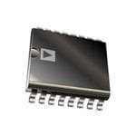
ICGOO电子元器件商城为您提供AD5504BRUZ由Analog设计生产,在icgoo商城现货销售,并且可以通过原厂、代理商等渠道进行代购。 AD5504BRUZ价格参考。AnalogAD5504BRUZ封装/规格:数据采集 - 数模转换器, 12 位 数模转换器 4 16-TSSOP。您可以下载AD5504BRUZ参考资料、Datasheet数据手册功能说明书,资料中有AD5504BRUZ 详细功能的应用电路图电压和使用方法及教程。
AD5504BRUZ 是由 Analog Devices Inc.(ADI)生产的一款 14 位、四通道电压输出数模转换器(DAC),属于数据采集 - 数模转换器类别。其主要应用场景包括以下领域:

 1. 工业自动化与控制
   - AD5504BRUZ 可用于工业自动化系统中,将数字信号转换为模拟信号以驱动执行器、阀门或电机控制器。
   - 在过程控制系统中,该 DAC 提供高精度的电压输出,用于调节压力、温度、流量等参数。

 2. 测试与测量设备
   - 在测试仪器(如信号发生器、校准仪)中,AD5504BRUZ 能生成精确的模拟信号,用于测试电子电路或传感器性能。
   - 其多通道设计支持同时生成多个独立的测试信号,提高测试效率。

 3. 通信系统
   - 在通信设备中,AD5504BRUZ 可用于生成调制信号或参考信号,支持无线通信和有线通信中的信号处理需求。
   - 其低功耗和小封装特点使其适合便携式或空间受限的通信应用。

 4. 医疗设备
   - 在医疗成像设备(如超声波机、X 射线机)中,AD5504BRUZ 可用于生成驱动信号以控制传感器或探测器。
   - 高精度的电压输出确保了医疗设备的测量结果更加准确可靠。

 5. 音频与多媒体设备
   - AD5504BRUZ 的高分辨率特性使其适用于高质量音频信号的数模转换,例如在专业音频设备或家庭影院系统中。
   - 它可以提供稳定的音频信号输出,减少失真和噪声。

 6. 汽车电子
   - 在汽车电子控制系统中,AD5504BRUZ 可用于生成模拟信号以驱动传感器或执行器,例如燃油喷射系统或悬架控制系统。
   - 其宽工作温度范围(-40°C 至 +125°C)使其能够在严苛的汽车环境中稳定运行。

 7. 消费类电子产品
   - 在家用电器或智能设备中,AD5504BRUZ 可用于控制显示屏亮度、调节音量或生成传感器驱动信号。
   - 其紧凑的 SOIC 封装形式适合小型化设计需求。

总之,AD5504BRUZ 凭借其高精度、低功耗和多通道特性,广泛应用于需要精确模拟信号生成的各种领域,满足不同行业对高性能数模转换的需求。
| 参数 | 数值 |
| 产品目录 | 集成电路 (IC)半导体 |
| 描述 | IC DAC 12BIT SPI 16-TSSOP数模转换器- DAC Quad CH 12-Bit VTG Output |
| DevelopmentKit | EVAL-AD5504EBZ |
| 产品分类 | |
| 品牌 | Analog Devices |
| 产品手册 | |
| 产品图片 |
|
| rohs | 符合RoHS无铅 / 符合限制有害物质指令(RoHS)规范要求 |
| 产品系列 | 数据转换器IC,数模转换器- DAC,Analog Devices AD5504BRUZ- |
| 数据手册 | |
| 产品型号 | AD5504BRUZ |
| 产品培训模块 | http://www.digikey.cn/PTM/IndividualPTM.page?site=cn&lang=zhs&ptm=18614http://www.digikey.cn/PTM/IndividualPTM.page?site=cn&lang=zhs&ptm=26125http://www.digikey.cn/PTM/IndividualPTM.page?site=cn&lang=zhs&ptm=26140http://www.digikey.cn/PTM/IndividualPTM.page?site=cn&lang=zhs&ptm=26150http://www.digikey.cn/PTM/IndividualPTM.page?site=cn&lang=zhs&ptm=26147 |
| 产品种类 | 数模转换器- DAC |
| 位数 | 12 |
| 供应商器件封装 | 16-TSSOP |
| 分辨率 | 12 bit |
| 包装 | 管件 |
| 商标 | Analog Devices |
| 安装类型 | 表面贴装 |
| 安装风格 | SMD/SMT |
| 封装 | Tube |
| 封装/外壳 | 16-TSSOP(0.173",4.40mm 宽) |
| 封装/箱体 | TSSOP-16 |
| 工作温度 | -40°C ~ 105°C |
| 工厂包装数量 | 96 |
| 建立时间 | 45µs |
| 接口类型 | SPI |
| 数据接口 | SPI™、QSPI™、MICROWIRE™ 和 DSP |
| 最大工作温度 | + 105 C |
| 最小工作温度 | - 40 C |
| 标准包装 | 1 |
| 电压参考 | Internal |
| 电压源 | 单电源 |
| 电源电压-最大 | 62 V |
| 电源电压-最小 | 10 V |
| 积分非线性 | +/- 1 LSB |
| 稳定时间 | 35 us |
| 系列 | AD5504 |
| 结构 | Resistor String |
| 设计资源 | |
| 转换器数 | 4 |
| 转换器数量 | 4 |
| 输出数和类型 | 4 电压,单极 |
| 输出类型 | Voltage |
| 采样率(每秒) | * |


- 商务部:美国ITC正式对集成电路等产品启动337调查
- 曝三星4nm工艺存在良率问题 高通将骁龙8 Gen1或转产台积电
- 太阳诱电将投资9.5亿元在常州建新厂生产MLCC 预计2023年完工
- 英特尔发布欧洲新工厂建设计划 深化IDM 2.0 战略
- 台积电先进制程称霸业界 有大客户加持明年业绩稳了
- 达到5530亿美元!SIA预计今年全球半导体销售额将创下新高
- 英特尔拟将自动驾驶子公司Mobileye上市 估值或超500亿美元
- 三星加码芯片和SET,合并消费电子和移动部门,撤换高东真等 CEO
- 三星电子宣布重大人事变动 还合并消费电子和移动部门
- 海关总署:前11个月进口集成电路产品价值2.52万亿元 增长14.8%


PDF Datasheet 数据手册内容提取
High Voltage, Quad-Channel 12-Bit Voltage Output DAC Data Sheet AD5504 FEATURES GENERAL DESCRIPTION Quad-channel high voltage DAC The AD5504 is a quad-channel, 12-bit, serial input, digital-to- 12-bit resolution analog converter with on-chip high voltage output amplifiers Pin selectable 30 V or 60 V output range and an integrated precision reference. The DAC output voltage Integrated precision reference ranges are programmable via the range select pin (R_SEL). If Low power serial interface with readback capability R_SEL is held high, the DAC output ranges are 0 V to 30 V. If Integrated temperature sensor alarm function R_SEL is held low, the DAC output ranges are 0 V to 60 V. The Power-on reset on-chip output amplifiers allow an output swing within the Simultaneous updating via LDAC range of AGND + 0.5 V to V − 0.5 V. DD Wide operating temperature: −40°C to +105°C The AD5504 has a high speed serial interface, which is com- APPLICATIONS patible with SPI®-, QSPI™-, MICROWIRE™-, and DSP-interface Programmable voltage sources standards and can handle clock speeds of up to 16.667 MHz. High voltage LED drivers Receiver bias in optical communications FUNCTIONAL BLOCK DIAGRAM CLRR_SELVLOGIC LDAC VDD REFERENCE 1713kΩ 122.36kΩ – SDI INPUT DAC VOUTA REGISTER REGISTER DACA + 12 A A 12 SDO 1713kΩ INPUT SCLK COLNOTGRICOL 122.36kΩ – SYNC INPUT DAC VOUTB REGISTER REGISTER DAC B + B B 12 ALARM 1713kΩ 122.36kΩ – POWER-ON RESET INPUT DAC VOUTC REGISTER REGISTER DAC C + C C 12 1713kΩ 122.36kΩ – INPUT DAC VOUTD REGISTER REGISTER DAC D + D D 12 AD5504 POWER-DOWN CONTROL LOGIC TEMPERATURE SENSOR DGND AGND 07994-001 Figure 1. Rev. B Document Feedback Information furnished by Analog Devices is believed to be accurate and reliable. However, no responsibility is assumed by Analog Devices for its use, nor for any infringements of patents or other One Technology Way, P.O. Box 9106, Norwood, MA 02062-9106, U.S.A. rights of third parties that may result from its use. Specifications subject to change without notice. No license is granted by implication or otherwise under any patent or patent rights of Analog Devices. Tel: 781.329.4700 ©2009-2012 Analog Devices, Inc. All rights reserved. Trademarks and registered trademarks are the property of their respective owners. Technical Support www.analog.com
AD5504 Data Sheet TABLE OF CONTENTS Features .............................................................................................. 1 Power-Down Mode .................................................................... 14 Applications ....................................................................................... 1 DAC Channel Architecture ....................................................... 14 General Description ......................................................................... 1 Selecting the Output Range ...................................................... 14 Functional Block Diagram .............................................................. 1 CLR Function.............................................................................. 14 Revision History ............................................................................... 2 LDAC Function .......................................................................... 14 Specifications ..................................................................................... 4 Temperature Sensor ................................................................... 15 AC Characteristics ........................................................................ 5 Power Dissipation....................................................................... 15 Timing Characteristics ................................................................ 6 Power Supply Sequencing ......................................................... 15 Absolute Maximum Ratings ............................................................ 8 Serial Interface ................................................................................ 16 Thermal Resistance ...................................................................... 8 Write Mode ................................................................................. 16 ESD Caution .................................................................................. 8 Read Mode .................................................................................. 16 Pin Configuration and Function Descriptions ............................. 9 Writing to the Control Register ................................................ 16 Typical Performance Characteristics ........................................... 10 Interfacing Examples ................................................................. 18 Terminology .................................................................................... 12 Outline Dimensions ....................................................................... 19 Theory of Operation ...................................................................... 14 Ordering Guide .......................................................................... 19 Power-Up State ........................................................................... 14 REVISION HISTORY 12/12—Rev. A to Rev. B Changes to t Parameter, Table 4 .................................................... 6 4 Changes to Figure 3 and Figure 4 ................................................... 7 Changes to Pin 3 Description, Table 7 and Pin 4 Description, Table 7 ................................................................................................ 9 Changes to Write Mode Section ................................................... 16 Changes to Table 10 ........................................................................ 17 10/10—Rev. 0 to Rev. A Changes to Figure 3 and Figure 4 ................................................... 7 7/09—Revision 0: Initial Version Rev. B | Page 2 of 20
Data Sheet AD5504 The serial interface offers the user the capability of both writing The AD5504 has an on-chip temperature sensor. When the to, and reading from, most of the internal registers. To reduce temperature on the die exceeds 110°C, the ALARM pin (an power consumption at power up, only the digital section of the active low CMOS output pin) flags an alarm and the AD5504 AD5504 is powered up initially. This gives the user the ability to enters a temperature power-down mode disconnecting the program the DAC registers to the required value while typically output amplifier thus removing the short-circuit condition. The only consuming 30 μA of supply current. The AD5504 incor- AD5504 remains in power-down mode until a software power-up porates power-on reset circuitry that ensures the DAC registers command is executed. power up in a known condition and remain there until a valid The AD5504 is available in a compact 16-lead TSSOP. The AD5504 write to the device has taken place. The analog section is is guaranteed to operate over the extended temperature range of powered up by issuing a power-up command via the SPI −40°C to +105°C. interface. The AD5504 provides software-selectable output loads while in the power-down mode. Table 1. Related Device Part No. Description AD5501 High Voltage, 12-Bit Voltage Output DAC Rev. B | Page 3 of 20
AD5504 Data Sheet SPECIFICATIONS V = 10 V to 62 V; V = 2.3 V to 5.5 V; R = 60 kΩ; C = 200 pF; −40°C < T < +105°C, unless otherwise noted. DD LOGIC L L A Table 2. Parameter Symbol Min Typ1 Max Unit Test Conditions/Comments ACCURACY2 Resolution 12 Bits Differential Nonlinearity DNL −1 1 LSB Integral Nonlinearity INL 60 V Mode −2 +2 LSB V = 62 V DD 30 V Mode −3 +3 LSB V = 62 V DD V Temperature Coefficient3, 4, 5 50 ppm/°C DAC code = half scale OUTX Zero-Scale Error V 100 mV DAC code = 0 ZSE Zero-Scale Error Drift4 60 µV/°C 60 V mode Offset Error6 V −80 +120 mV OE Offset Error Drift4 60 µV/°C 60 V mode Full-Scale Error V −325 +275 mV FSE Full-Scale Error Drift4 1 mV/°C −40°C to +25°C; 60 V mode 350 µV/°C +25°C to +105°C; 60 V mode Gain Error −0.6 +0.6 % of FSR Gain Temperature Coefficient4 10 ppm of FSR/°C 60 V mode DC Crosstalk4 R = 60 kΩ to AGND or V L DD Due to Single Channel Full-Scale 3 mV 60 V mode Output Change Due to Powering Down (Per Channel) 4 mV 60 V mode OUTPUT CHARACTERISTICS Output Voltage Range7 AGND + 0.5 V − 0.5 V DD Short-Circuit Current4, 8 2 mA On any single channel Capacitive Load Stability4 1 V to 4 V step R = 60 kΩ to ∞ 1 nF L Load Current4 −1 +1 mA On any single channel DC Output Impedance4 3 Ω DC Output Leakage4 10 µA DIGITAL INPUTS Input Logic High V 2.0 V V = 4.5 V to 5.5 V IH LOGIC 1.8 V V = 2.3 V to 3.6 V LOGIC Input Logic Low V 0.8 V V = 2.3 V to 5.5 V IL LOGIC Input Current I ±1 µA IL Input Capacitance4 I 5 pF IC DIGITAL OUTPUTS Output High Voltage V V − 0.4 V V I = 200 µA OH LOGIC SOURCE Output Low Voltage V DGND + 0.4 V V I = 200 µA OL SINK Three-State Leakage Current SDI, SDO, SCLK, LDAC, CLR, R_SEL −1 +1 µA ALARM −10 +10 µA Output Capacitance4 5 pF Rev. B | Page 4 of 20
Data Sheet AD5504 Parameter Symbol Min Typ1 Max Unit Test Conditions/Comments POWER SUPPLIES V 10 62 V DD V 2.3 5.5 V LOGIC Quiescent Supply Current (I ) 2 3 mA Static conditions; DAC QUIESCENT outputs = midscale Logic Supply Current (I ) 0.4 2 µA V = V ; V = DGND LOGIC IH LOGIC IL DC PSRR4 DAC output = full-scale 60 V Mode 68 dB 30 V Mode 76 dB POWER-DOWN MODE Supply Current I DD_PWD Software Power-Down Mode 30 50 µA Junction Temperature8 T 130 °C T = T + P × θ J J A TOTAL JA 1 Typical specifications represent average readings at 25°C, VDD = 62 V and VLOGIC = 5 V. 2 Valid in output voltage range of (VDD − 0.5 V) to (AGND + 0.5 V). Outputs are unloaded. 3 Includes linearity, offset, and gain drift. 4 Guaranteed by design and characterization. Not production tested. 5 VOUTX refers to VOUTA, VOUTB, VOUTC, or VOUTD. 6 DAC code = 32 for 60 V mode; DAC code = 64 for 30 V mode. 7 The DAC architecture gives a fixed linear voltage output range of 0 V to 30 V if R_SEL is held high and 0 V to 60 V if R_SEL is held low. As the output voltage range is limited by output amplifier compliance, VDD should be set to at least 0.5 V higher than the maximum output voltage to ensure compliance. 8 If the die temperature exceeds 110°C, the AD5504 enters a temperature power-down mode putting the DAC outputs into a high impedance state thereby removing the short-circuit condition. Overheating caused by long term short-circuit condition(s) is detected by an integrated thermal sensor. After power-down, the AD5504 stays powered down until a software power-up command is executed. AC CHARACTERISTICS V = 10 V to 62 V; V = 2.3 V to 5.5 V; R = 60 kΩ; C = 200 pF; −40°C < T < +105°C, unless otherwise noted. DD LOGIC L L A Table 3. Parameter1, 2 Min Typ Max Unit Test Conditions/Comments3 AC CHARACTERISTICS Output Voltage Settling Time ¼ to ¾ scale settling to ±1 LSB, R = 60 kΩ L 60 V Mode 45 55 µs 30 V Mode 25 35 µs Slew Rate 0.65 V/µs Digital-to-Analog Glitch Energy 300 nV-s 1 LSB change around major carry in 60 V mode Glitch Impulse Peak Amplitude 170 mV 60 V mode Digital Feedthrough 40 nV-s Digital Crosstalk 5 nV-s Analog Crosstalk 600 nV-s DAC-to-DAC Crosstalk 600 nV-s Peak-to-Peak Noise 140 μV p-p 0.1 Hz to 10 Hz; DAC code = 0x800 4 mV p-p 0.1 Hz to 10 kHz; DAC code = 0x800 1 Guaranteed by design and characterization; not production tested. 2 See the Terminology section. 3 Temperature range is −40°C to + 105°C, typical at 25°C. Rev. B | Page 5 of 20
AD5504 Data Sheet TIMING CHARACTERISTICS V = 30 V, V = 2.3 V to 5.5 V and −40°C < T < +105°C; all specifications T to T , unless otherwise noted. DD LOGIC A MIN MAX Table 4. Parameter Limit1 Unit Test Conditions/Comments t 2 60 ns min SCLK cycle time 1 t 10 ns min SCLK high time 2 t 10 ns min SCLK low time 3 t4 25 ns min SYNC falling edge to SCLK rising edge setup time t 15 ns min Data setup time 5 t 5 ns min Data hold time 6 t7 0 ns min SCLK falling edge to SYNC rising edge t8 20 ns min Minimum SYNC high time t9 20 ns min LDAC pulse width low t10 50 ns min SCLK falling edge to LDAC rising edge t11 15 ns min CLR pulse width low t12 100 ns typ CLR pulse activation time t13 20 μs typ ALARM clear time t 110 ns min SCLK cycle time in read mode 14 t 3 55 ns max SCLK rising edge to SDO valid 15 t 3 25 ns min SCLK to SDO data hold time 16 t 4 50 μs max Power-on reset time (this is not shown in the timing diagrams) 17 t 5 50 μs max Power-on time (this is not shown in the timing diagrams) 18 t19 5 μs typ ALARM clear to output amplifier turn on (this is not shown in the timing diagrams) 1 All input signals are specified with tr = tf = 1 ns/V (10% to 90% of VDD) and timed from a voltage level of (VIL + VIH)/2. 2 Maximum SCLK frequency is 16.667 MHz. 3 Under load conditions shown in Figure 2. 4 Time from when the VDD/VLOGIC supplies are powered-up to when a digital interface command can be executed. 5 Time required from execution of power-on software command to when the DAC outputs have settled to 1 V. 200µA IOL TO OUTPUT VOH (MIN) – VOL (MAX) PIN CL 2 50pF 200µA IOH 07994-002 Figure 2. Load Circuit for SDO Timing Diagram Rev. B | Page 6 of 20
Data Sheet AD5504 t4 t1 SCLK t8 t3 t2 t7 SYNC t6 t5 SDI R/W D0 t9 LDAC1 t10 LDAC2 t11 CLR t13 ALARM3 t12 VOUTx4 1ASYNCHRONOUS LDAC UPDATE MODE. 234SIVNYO TUNHTCxEH R REEOVFENENORTUS SO T FLO DO AAVNCEY RU OTPEFD MAVPOTEUETR MAA,O TVDUOERU.ETB C, OVONUDTICT IOORN .VOUTD. 07994-003 Figure 3. Write Timing Diagram t14 SCLK SYNC SDI R/W A2 A1 A0 X X X X X X X t15 t16 SDO D11 D10 D9 D8 D2 D1 D0 07994-004 Figure 4. Read Timing Diagram Rev. B | Page 7 of 20
AD5504 Data Sheet ABSOLUTE MAXIMUM RATINGS THERMAL RESISTANCE T = 25°C, unless otherwise noted. Transient currents of up to A 100 mA do not cause SCR latch-up. θ is specified for the worst-case conditions, that is, a device JA soldered in a circuit board for surface-mount packages. Table 5. Thermal resistance is for a JEDEC 4-layer(2S2P) board. Parameter Rating V to AGND −0.3 V, + 64 V Table 6. Thermal Resistance DD VLOGIC to DGND −0.3 V to +7 V Package Type θJA Unit VOUTX to AGND1 −0.3 V to VDD + 0.3 V 16-Lead TSSOP 112.60 °C/W Digital Input to DGND −0.3 V to V + 0.3 V LOGIC SDO Output to DGND −0.3 V to VLOGIC + 0.3 V ESD CAUTION AGND to DGND −0.3 V to +0.3 V Maximum Junction Temperature 150°C (T Maximum) J Storage Temperature Range −65°C to +150°C Reflow Soldering Peak Temperature 260°C Time at Peak Temperature Range 20 sec to 40 sec 1 VOUTX refers to VOUTA, VOUTB, VOUTC, or VOUTD. Stresses above those listed under Absolute Maximum Ratings may cause permanent damage to the device. This is a stress rating only; functional operation of the device at these or any other conditions above those indicated in the operational section of this specification is not implied. Exposure to absolute maximum rating conditions for extended periods may affect device reliability. Rev. B | Page 8 of 20
Data Sheet AD5504 PIN CONFIGURATION AND FUNCTION DESCRIPTIONS CLR 1 16 VLOGIC SYNC 2 15 ALARM SCLK 3 AD5504 14 VDD SDI 4 TOP VIEW 13 R_SEL (Not to Scale) SDO 5 12 VOUTA DGND 6 11 VOUTB AGND 7 10 VOUTC LDAC 8 9 VOUTD 07994-005 Figure 5. Pin Configuration Table 7. Pin Function Descriptions Pin No. Mnemonic Description 1 CLR Asynchronous Clear Input. The CLR input is falling edge sensitive. When CLR is low, all LDAC pulses are ignored. When CLR is activated, the input register and the DAC register are set to 0x000 and the outputs to zero scale. 2 SYNC Falling Edge Synchronization Signal. This is the frame synchronization signal for the input data. When SYNC goes low, it enables the input shift register and data is transferred in on the rising edges of the following clocks. The selected DAC register is updated on the 16th falling SCLK, unless SYNC is taken high before this edge, in which case, the rising edge of SYNC acts as an interrupt, and the write sequence is ignored by the DAC. 3 SCLK Serial Clock Input. Data is clocked into the input shift register on the rising edge of the serial clock input. Data can be transferred at rates up to 16 MHz. 4 SDI Serial Data Input. This part has a 16-bit shift register. Data is clocked into the register on the rising edge of the serial clock input. 5 SDO Serial Data Output. CMOS output. This pin serves as the readback function for all DAC and control registers. Data is clocked out on the rising edge of SCLK and is valid on the falling edge of SCLK. 6 DGND Digital Ground Pin. 7 AGND Analog Ground Pin. 8 LDAC Load DAC Input. Pulsing this pin low allows any or all DAC registers to be updated if the input registers have new data. This allows all DAC outputs to update simultaneously. Alternatively, this pin can be tied permanently low. 9 V Buffered Analog Output Voltage from DAC D. OUTD 10 V Buffered Analog Output Voltage from DAC C. OUTC 11 V Buffered Analog Output Voltage from DAC B. OUTB 12 V Buffered Analog Output Voltage from DAC A. OUTA 13 R_SEL Range Select Pin. Tying this pin to DGND selects a DAC output range of 0 V to 60 V, alternatively tying R_SEL to V selects a DAC output range of 0 V to 30 V. LOGIC 14 V Positive Analog Power Supply. 10 V to 62 V for the specified performance. This pin should be decoupled with 0.1 µF DD ceramic capacitors and 10 µF capacitors. 15 ALARM Active Low CMOS Output Pin. This pin flags an alarm if the temperature on the die exceeds 110°C. 16 V Logic Power Supply; 2.3 V to 5.5 V. Decouple this pin with 0.1µF ceramic capacitors and 10 µF capacitors. LOGIC Rev. B | Page 9 of 20
AD5504 Data Sheet TYPICAL PERFORMANCE CHARACTERISTICS 0.8 45.0025 0.4 45.0000 B) V) NL (LS 0 (OUTX44.9975 I V –0.4 44.9950 –0.8 44.9925 32 1008 C2O04D8E 3056 4064 07994-006 0 0.05 TIM0E.1 (0ms) 0.15 0.20 07994-009 Figure 6. Typical INL Figure 9. Output Settling Time (Low to High) 0.50 200 VDD = 62V VOUTx = 30V 0.25 V) 100 µ E ( DNL (LSB) 0 T VOLTAG 0 U P T U O –0.25 –100 –0.5032 1008 C2O04D8E 3056 4064 07994-007 –2000 2.5 TIME (S5.e0conds) 7.5 10.0 07994-010 Figure 7. Typical DNL Figure 10. Output Noise 15.0050 0.70 VDD = 62V VOUTB, VOUTC, AND VOUTD POWERED DOWN 15.0025 0.65 V (V)OUTX15.0000 I (mA)DD0.60 14.9975 0.55 14.9950 0.50 0 0.05 TIM0E.1 (0ms) 0.15 0.20 07994-008 0 15 VOU3T0A (V) 45 60 07994-011 Figure 8. Output Settling Time (High to Low) Figure 11. IDD vs. VOUTA Rev. B | Page 10 of 20
Data Sheet AD5504 2.2 0.20 VDD = 62V VOUTA = VOUTB = VOUTC = VOUTD 0.15 2.1 0.10 0.05 A) ΔV) I (mDD 2.0 V (OUTA 0 –0.05 1.9 –0.10 VOUTA = 30V; VOUTB SWITCHING –0.15 VOUTB = 0V TO 30V VOUTB = 0V TO 45V VOUTB = 0V TO 60V 1.8 –0.20 0 15 OUTPUT V3O0LTAGE (V) 45 60 07994-012 0 2 4TIME (µs)6 8 10 07994-202 Figure 12. IDD vs. VOUTA to VOUTD Figure 15. DAC-to-DAC Crosstalk 2 6 VOUTD 0 5 B) –2 4 LS VOUTB LITUDE ( –4 LSBs 3 P M A –6 2 VOUTC –8 1 VOUTA –100 5 TIME (ms) 10 15 07994-013 0–1.0 –0.5 LOAD CUR0RENT (mA) 0.5 1.0 07994-201 Figure 13. Digital-to-Analog Negative Glitch Impulse Figure 16. DAC-to-DAC Mismatch 12 10 8 B) S 6 L E ( UD 4 T LI P M 2 A 0 –2 –4 0 5 TIME (ms) 10 15 07994-014 Figure 14. Digital-to-Analog Positive Glitch Impulse Rev. B | Page 11 of 20
AD5504 Data Sheet TERMINOLOGY Relative Accuracy Gain Temperature Coefficient For the DAC, relative accuracy, or integral nonlinearity (INL), The gain temperature coefficient is a measure of the change in is a measure of the maximum deviation in LSBs from a straight gain with changes in temperature. It is expressed in (ppm of line passing through the endpoints of the DAC transfer function. full-scale range)/°C. Differential Nonlinearity Digital-to-Analog Glitch Impulse Differential nonlinearity (DNL) is the difference between the Digital-to-analog glitch impulse is the impulse injected into the measured change and the ideal 1 LSB change between any two analog output when the input code in the DAC register changes adjacent codes. A specified differential nonlinearity of ±1 LSB state. It is normally specified as the area of the glitch in nV-s maximum ensures monotonicity. This DAC is guaranteed mono- and is measured when the digital input code is changed by tonic by design. 1 LSB at the major carry transition. Zero-Code Error DC and AC Power Supply Rejection Ratio (PSRR) Zero-code error is a measure of the output error when zero PSRR indicates how the output of the DAC is affected by changes code (0x000) is loaded into the DAC register. Ideally, the output in the supply voltage. PSRR is the ratio of the change in V , OUTA should be 0 V. The zero-code error is always positive in the V , V , or V to a change in V for full-scale output of OUTB OUTC OUTD DD AD5504 because the output of the DAC cannot go below 0 V. the DAC. It is measured in decibels. For dc PSRR, V is dc DD It is due to a combination of the offset errors in the DAC and varied ±10%. For ac PSRR, V is ac varied ±10%. DD output amplifier. Zero-code error is expressed in millivolts. DC Crosstalk Zero-Code Error Drift DC crosstalk is the dc change in the output level of one DAC in Zero-code error drift is a measure of the change in zero-code response to a change in the output of another DAC. It is measured error with a change in temperature. It is expressed in μV/°C. with a full-scale output change on one DAC (or soft power-down and power-up) while monitoring another DAC kept at midscale. Offset Error It is expressed in millivolts. A measure of the difference between V (actual) and V OUT OUT DC crosstalk due to load current change is a measure of the (ideal) expressed in millivolts in the linear region of the transfer impact that a change in load current on one DAC has to another function. Offset error is measured on the AD5504 with Code 32 DAC kept at midscale. It is expressed in μV/mA. loaded in the DAC registers for 60 V mode and with Code 64 loaded in the DAC registers for 30 V mode. Offset error is Digital Feedthrough expressed in millivolts. Digital feedthrough is a measure of the impulse injected into the analog output of a DAC from the digital input pins of the Offset Error Drift device but is measured when the DAC is not being written to Offset error drift is a measure of the change in offset error with (SYNC held high). It is specified in nV-s and measured with a a change in temperature. It is expressed in μV/°C. full-scale change on the digital input pins, that is, from all 0s to Full-Scale Error all 1s or vice versa. Full-scale error is a measure of the output error when full-scale Analog Crosstalk code (0xFFF) is loaded into the DAC register. Full-scale error is Analog crosstalk is the glitch impulse transferred to the output expressed in millivolts. of one DAC due to a change in the output of another DAC. It is Full-Scale Error Drift measured by loading one of the input registers with a full-scale Full-scale error drift is a measure of the change in full-scale code change (all 0s to all 1s or vice versa) while keeping LDAC error with a change in temperature. It is expressed in μV/°C. high, and then pulsing LDAC low and monitoring the output of Gain Error the DAC whose digital code has not changed. The area of the Gain error is a measure of the span error of the DAC. It is the glitch is expressed in nV-s. deviation in slope of the DAC transfer characteristic from the ideal, expressed as a percentage of the full-scale range. Rev. B | Page 12 of 20
Data Sheet AD5504 DAC-to-DAC Crosstalk Capacitive Load Stability DAC-to-DAC crosstalk is the glitch impulse transferred to the Capacitive load stability refers to the ability of the amplifier to output of one DAC due to a digital code change and subsequent drive a capacitive load. An amplifier output is considered stable output change of another DAC. This includes both digital and if any overshoot or ringing has stopped before approximately analog crosstalk. It is measured by loading one of the DACs 1.5 times the settling time of the DAC has elapsed. with a full-scale code change (all 0s to all 1s or vice versa) with LDAC low and monitoring the output of another DAC. The energy of the glitch is expressed in nV-s. Rev. B | Page 13 of 20
AD5504 Data Sheet THEORY OF OPERATION The AD5504 contains four DACs, four output amplifiers, and a format for the AD5501 is straight binary and the output voltage precision reference in a single package. The architecture of a follows the formula single DAC channel consists of a 12-bit resistor string DAC D V = ×Range followed by an output buffer amplifier. The part operates from OUT 4096 a single-supply voltage of 10 V to 62 V. The DAC output voltage where: range is selected via the range select, R_SEL, pin. The DAC D is the code loaded to the DAC. output range is 0 V to 30 V if R_SEL is held high and 0 V to Range = 30, if R_SEL is high, and 60 if R_SEL is low. 60 V if R_SEL is held low. Data is written to the AD5504 in a 16-bit word format (see Table 8), via a serial interface. PRECISION REFERENCE POWER-UP STATE On power-up, the power-on reset circuitry clears the bits of the REINGPISUTTER REGDIASCTER DAC GAIN VOUTx control register to 0x40 (see Table 10). This ensures that the 12 12 apnoawloerg csoenctsiuomn pist iionnit.i aTlhlye puoswere creadn dporowgnr,a mwh tihceh DheAlpCs rreegdiustceer s AGND 07994-015 to the required values while typically consuming only 30 µA of Figure 17. DAC Channel Architecture (Single-Channel Shown) supply current. The power-on reset circuitry also ensures that all the input and DAC registers power up in a known condition, SELECTING THE OUTPUT RANGE 0x000, and remain there until a valid write to the device has The output range of the DACs is selected by the R_SEL pin. taken place. The analog section can be powered up by setting When the R_SEL pin is connected to Logic 1, the DAC output any or all of Bit C2 to Bit C5 of the control register to 1. voltages can be set between 0 V and 30 V. When the R_SEL pin POWER-DOWN MODE is connected to Logic 0, the DAC output voltages can be set Each DAC channel can be individually powered up or powered between 0 V and 60 V. The state of R_SEL can be changed any down by programming the control register (see Table 10). time when the serial interface is not being used, that is, not When the DAC channel is powered down, the associated analog during a read or write operation. When the R_SEL pin is circuitry turns off to reduce power consumption. The digital changed, the voltage on the output pin remains the same until section of the AD5504 remains powered up. The output of the the next write to the DAC register (and LDAC is brought low). DAC amplifier can be three-stated or connected to AGND via For example, if the user writes 0x800 to the DAC register when an internal 20 kΩ resistor, depending on the state of Bit C6 in in 30 V mode (R_SEL = 1), the output voltage is 15 V (assuming the control register. The power-down mode does not change the LDAC is low or has been pulsed low). When the user switches contents of the DAC register to ensure that the DAC channel to 60 V mode (R_SEL = 0), the output stays at 15 V until the returns to its previous voltage when the power-down bit is set to 1. user writes a new value to the DAC register. LDAC must be low The AD5504 also offers the user the flexibility of updating the or be pulsed low for the output to change. DAC registers during power-down. The control register can be read back at any time to check the status of the bits. CLR FUNCTION DAC CHANNEL ARCHITECTURE The AD5504 has a hardware CLR pin that is an asynchronous The architecture of a single DAC channel consists of a 12-bit clear input. The CLR input is falling edge sensitive. Bringing the resistor string DAC followed by an output buffer amplifier (see CLR line low clears the contents of the input register and the Figure 17). The resistor string section is simply a string of DAC registers to 0x000. The CLR pulse activation time, that is, resistors, each of Value R from V generated by the precision REF the falling edge of CLR to when the output starts to change, is reference to AGND. This type of architecture guarantees DAC typically 100 ns. monotonicity. The 12-bit binary digital code loaded to the DAC LDAC FUNCTION register determines at which node on the string the voltage is tapped off before being fed into the output amplifier. The The DAC outputs can be updated using the hardware LDAC output amplifier multiplies the DAC output voltage to give a pin. LDAC is normally high. On the falling edge of LDAC, data fixed linear voltage output range of 0 V to 60 V if R_SEL = 0 is copied from the input registers to the DAC registers, and the or 0 V to 30 V if R_SEL = 1. Each output amplifier is capable DAC outputs are updated simultaneously (asynchronous update of driving a 60 kΩ load while allowing an output swing within mode, see Figure 3). If the LDAC is kept low, or is low on the the range of AGND + 0.5 V and VDD − 0.5 V. falling edge of the 16th SCLK, the appropriate DAC register and Because the DAC architecture gives a fixed voltage output range DAC output are updated automatically (synchronous update of 0 V to 30 V or 0 V to 60 V, the user should set VDD to at least mode, see Figure 3). 30.5 V or 60.5 V to use the maximum DAC resolution. The data Rev. B | Page 14 of 20
Data Sheet AD5504 TEMPERATURE SENSOR The amount of heat generated can be calculated using the formula The AD5504 has an integrated temperature sensor that causes the part to enter thermal shutdown mode when the temperature TJ = TA + (PTOTAL × θJA) on the die exceeds 110°C. In thermal shutdown mode, the where: analog section of the device powers down and the DAC outputs T is the package junction temperature. J are disconnected, but the digital section remains operational, T is the ambient temperature. A which is equivalent to setting the power-down bit in the control P is the total power being consumed by the AD5504. TOTAL register. To indicate that the AD5504 has entered temperature θ is the thermal impedance of the AD5504 package (see the JA shutdown mode, Bit 0 of the control register is set to 1 and the Absolute Maximum Ratings section for this value). ALARM pin goes low. The AD5504 remains in temperature POWER SUPPLY SEQUENCING shutdown mode with Bit 0 set to 1 and the ALARM pin low, even if the die temperature falls, until Bit 0 in the control register is The power supplies for the AD5504 can be applied in any order cleared to 0. without affecting the device. However, the AGND and DGND POWER DISSIPATION pins should be connected to the relevant ground plane before the power supplies are applied. None of the digital input pins Drawing current from any of the voltage output pins causes a (SCLK, SDI, SYNC, R_SEL and CLR) should be allowed to float temperature rise in the die and package of the AD5504. The during power up. The digital input pins can be connected to package junction temperature (T) should not exceed 130°C for J pull-up (to V ) or pull-down (to DGND) resistors as LOGIC normal operation. If the die temperature exceeds 110°C, the required. AD5504 enters thermal shutdown mode as described in the Temperature Sensor section. Rev. B | Page 15 of 20
AD5504 Data Sheet SERIAL INTERFACE The AD5504 has a serial interface (SYNC, SCLK, SDI, and READ MODE SDO), which is compatible with SPI interface standards, as well The AD5504 allows data readback via the serial interface from with as most DSPs. The AD5504 allows writing of data, via the every register directly accessible to the serial interface, which is serial interface, to the input and control registers. The DAC all registers except the DAC registers. To read back a register, it registers are not directly writeable or readable. is first necessary to tell the AD5504 that a readback is required. The input shift register is 16 bits wide (see Table 8). The 16-bit This is achieved by setting the R/W bit to 1. The three address word consists of one read/write (R/W) control bit, followed by bits then determine the register from which data is to be read three address bits and 12 DAC data bits. Data is loaded MSB first. back. Data from the selected register is then clocked out of the SDO pin on the next twelve clocks of the same frame. WRITE MODE The SDO pin is normally three-stated but becomes driven on To write to a register, the R/W bit should be 0. The three the rising edge of the fifth clock pulse. The pin remains driven address bits in the input register (see Table 9) then determine until the data from the register has been clocked out or the the register to update. The address bits (A2 to A0) are used for SYNC pin is returned high. Figure 4 shows the timing either DAC register selection or for writing to the control requirements during a read operation. Note that due to timing register. Data is clocked into the selected register during the requirements of t (110 ns), the maximum speed of the SPI remaining 12 clocks of the same frame. Figure 3 shows a timing 14 interface during a read operation should not exceed 9 MHz. diagram of a typical AD5504 write sequence. The write sequence begins by bringing the SYNC line low. Data on the WRITING TO THE CONTROL REGISTER SDI line is clocked into the 16-bit shift register on the rising The control register is written when Bits[DB14:DB12] are 1. edge of SCLK. On the 16th falling clock edge, the last data bit is The control register sets the power-up state of the DAC outputs. clocked in and the programmed function is executed (that is, a A write to the control register must be followed by another change in the selected DAC/DACs input register/registers or a write operation. The second write operation can be a write to a change in the mode of operation). The AD5504 does not DAC input register or a NOP write. Figure 18 shows some require a continuous SCLK and dynamic power can be saved by typical combinations. transmitting clock pulses during a serial write only. At this stage, the SYNC line can be kept low or be brought high. In either case, it must be brought high for a minimum of 20 ns before the next write sequence for a falling edge of SYNC to initiate the next write sequence. Operate all interface pins close to the supply rails to minimize power consumption in the digital input buffers. Table 8. Input Register Bit Map DB15 DB14 DB13 DB12 DB11 DB10 DB9 DB8 DB7 DB6 DB5 DB4 DB3 DB2 DB1 DB0 R/W A2 A1 A0 Data Table 9. Input Register Bit Functions Bit Description R/W Indicates a read from or a write to the addressed register. A2, A1, A0 These bits determine if the input registers or the control register are to be accessed. A2 A1 A0 Function/Address 0 0 0 No operation 0 0 1 DAC A input register 0 1 0 DAC B input register 0 1 1 DAC C input register 1 0 0 DAC D input register 1 0 1 Write data contents to all four DAC input registers 1 1 0 Reserved 1 1 1 Control register D11:D0 Data bits Rev. B | Page 16 of 20
Data Sheet AD5504 Table 10. Control Register Functions DB15 DB14 DB13 DB12 DB11 DB10 DB9 DB8 DB7 DB6 DB5 DB4 DB3 DB2 DB1 DB01 R/W 1 1 1 0 0 0 0 0 C6 C5 C4 C3 C2 C1 C0 1 Read-only bit. This bit should be 0 when writing to the control register. Table 11. Control Register Function Bit Descriptions Bit No. Bit Name Description DB0 C0 C0 = 0: the device is not in thermal shutdown mode. C0 = 1: the device is in thermal shutdown mode. DB1 C1 C1 = 0: reserved. This bit should be 0 when writing to the control register. DB2 C21 C2 = 0: DAC Channel A power-down (default). C2 = 1: DAC Channel A power-up. DB3 C31 C3 = 0: DAC Channel B power-down (default). C3 = 1: DAC Channel B power-up. DB4 C41 C4 = 0: DAC Channel C power-down (default). C4 = 1: DAC Channel C power-up. DB5 C51 C5 = 0: DAC Channel D power-down (default). C5 = 1: DAC Channel D power-up. DB6 C6 C6 = 0: outputs connected to AGND through a 20 kΩ resistor (default). C6 = 1: outputs are three-stated. 1 If Bit C2 to Bit C5 are set to 0, the part is placed in power-down mode. CONTWRORILT ER ETGOISTER NOP WRITE TO WRITE TO CONTROL REGISTER DAC REGISTER CONTWRORILT ER ETGOISTER CONTWRORILT ER ETGOISTER NOP WRITE TO WRITE TO WRITE TO CONTRWORLI TREE NGISTER CONTWRROITLE R NE G+ I1STER DAWCR RITEEG NIS +T E2R 07994-120 Figure 18. Control Register Write Sequences Rev. B | Page 17 of 20
AD5504 Data Sheet INTERFACING EXAMPLES The Analog Devices ADSP-21065L is a floating point DSP with two serial ports (SPORTs). Figure 20 shows how one SPORT The SPI interface of the AD5504 is designed to allow it to be can be used to control the AD5504. In this example, the transmit easily connected to industry-standard DSPs and microcon- frame synchronization (TFS) pin is connected to the receive trollers. Figure 19 shows how the AD5504 can be connected to frame synchronization (RFS) pin. The transmit and receive the Analog Devices, Inc., Blackfin® DSP. The Blackfin has an clocks (TCLK and RCLK) are also connected together. The user integrated SPI port that can be connected directly to the SPI can write to the AD5504 by writing to the transmit register. When a pins of the AD5504. Programmable input/output pins are also read operation is performed, the data is clocked out of the AD5504 available and can be used to read or set the state of the digital on the last 12 SCLKs. The DSP receive interrupt can be used to input or output pins associated with the interface. indicate when the read operation is complete. AD5504 ADSP-21065L AD5504 SPISELx SYNC TFSx SCK SCLK RFSx SYNC MOSI SDI TCLKx RCLKx SCLK MISO SDO DTxA SDI PF10 R_SEL DRxA SDO ADSP-BF531 PF9 LDAC FLAG0 R_SEL PF8 CLR FLAG1 LDAC Figure 19. PInFt7erfacing to a Blackfin DASPLA RM 07994-016 FFLLAAGG23 CALLRARM 07994-017 Figure 20. Interfacing to an ADSP-21065L DSP Rev. B | Page 18 of 20
Data Sheet AD5504 OUTLINE DIMENSIONS 5.10 5.00 4.90 16 9 4.50 6.40 4.40 BSC 4.30 1 8 PIN 1 1.20 MAX 0.15 0.20 0.05 0.09 0.75 0.30 8° 0.60 B0.S6C5 0.19 SPELAANTIENG 0° 0.45 COPLANARITY 0.10 COMPLIANT TO JEDEC STANDARDS MO-153-AB Figure 21. 16-Lead Thin Shrink Small Outline Package [TSSOP] (RU-16) Dimensions shown in millimeters ORDERING GUIDE Model1 Temperature Range Package Description Package Option AD5504BRUZ −40°C to +105°C 16-Lead Thin Shrink Small Outline Package [TSSOP] RU-16 AD5504BRUZ-REEL −40°C to +105°C 16-Lead Thin Shrink Small Outline Package [TSSOP] RU-16 EVAL-AD5504EBZ Evaluation Board 1 Z = RoHS Compliant Part.. Rev. B | Page 19 of 20
AD5504 Data Sheet NOTES ©2009-2012 Analog Devices, Inc. All rights reserved. Trademarks and registered trademarks are the property of their respective owners. D07994-0-12/12(B) Rev. B | Page 20 of 20
Mouser Electronics Authorized Distributor Click to View Pricing, Inventory, Delivery & Lifecycle Information: A nalog Devices Inc.: EVAL-AD5504EBZ AD5504BRUZ AD5504BRUZ-REEL