ICGOO在线商城 > 集成电路(IC) > 数据采集 - 数模转换器 > LTC2612IMS8#PBF

 Datasheet下载
- 型号: LTC2612IMS8#PBF
- 制造商: LINEAR TECHNOLOGY
- 库位|库存: xxxx|xxxx
- 要求:
| 数量阶梯 | 香港交货 | 国内含税 |
| +xxxx | $xxxx | ¥xxxx |
查看当月历史价格
查看今年历史价格
LTC2612IMS8#PBF产品简介:
ICGOO电子元器件商城为您提供LTC2612IMS8#PBF由LINEAR TECHNOLOGY设计生产,在icgoo商城现货销售,并且可以通过原厂、代理商等渠道进行代购。 LTC2612IMS8#PBF价格参考。LINEAR TECHNOLOGYLTC2612IMS8#PBF封装/规格:数据采集 - 数模转换器, 14 位 数模转换器 2 8-MSOP。您可以下载LTC2612IMS8#PBF参考资料、Datasheet数据手册功能说明书,资料中有LTC2612IMS8#PBF 详细功能的应用电路图电压和使用方法及教程。
LTC2612IMS8#PBF 是 Linear Technology(现为 Analog Devices)生产的一款 12 位电压输出数模转换器(DAC)。它属于数据采集系统中的数模转换器类别,广泛应用于需要精确控制模拟信号的场景。以下是其主要应用场景:

 1. 工业自动化与控制
   - 在工业自动化中,LTC2612 可用于生成精确的模拟控制信号,例如调节电机速度、阀门开度或温度控制器。
   - 它适用于可编程逻辑控制器(PLC)、分布式控制系统(DCS)和过程控制设备。

 2. 测试与测量设备
   - LTC2612 能够提供高精度的电压输出,适用于各种测试与测量仪器,如信号发生器、示波器校准设备和数据记录仪。
   - 其低功耗和小封装特点使其非常适合便携式测试设备。

 3. 通信系统
   - 在通信领域,LTC2612 可用于生成调制信号或基准电压,支持无线通信设备中的射频(RF)和中频(IF)信号处理。
   - 它还可以用作功率放大器的偏置电压源,确保稳定的工作状态。

 4. 医疗设备
   - 医疗设备中需要精确的模拟信号生成,例如超声波设备、心电图(ECG)设备和患者监护仪。
   - LTC2612 的高分辨率和低漂移特性使其适合这些对精度要求极高的应用。

 5. 消费电子
   - 在音频设备中,LTC2612 可用于数字音量控制或生成音频参考信号。
   - 它还可用于智能家居设备中的传感器接口,将数字信号转换为模拟信号以驱动执行器。

 6. 汽车电子
   - 在汽车电子系统中,LTC2612 可用于生成控制信号,例如调节车灯亮度、座椅加热器功率或空调系统的温度设置。
   - 它还适用于车载信息娱乐系统中的音频和视频信号处理。

 7. 航空航天与国防
   - 在航空航天领域,LTC2612 可用于导航系统、飞行控制和遥感设备中的信号生成和控制。
   - 其高可靠性和宽工作温度范围(-40°C 至 +125°C)使其适合严苛环境下的应用。

 特性总结
- 12 位分辨率:提供高精度的模拟信号输出。
- 单电源供电:简化电路设计,降低功耗。
- 小型 MSOP-8 封装:节省 PCB 空间,适合紧凑型设计。
- 内置输出缓冲放大器:减少对外部元件的需求,提高系统集成度。

总之,LTC2612IMS8#PBF 是一款性能优异的 DAC,适用于需要高精度、低功耗和小型化设计的各种应用场景。
| 参数 | 数值 |
| 产品目录 | 集成电路 (IC) |
| 描述 | IC DAC 14BIT DUAL R-R VOUT 8MSOP |
| 产品分类 | |
| 品牌 | Linear Technology |
| 数据手册 | http://www.linear.com/docs/1068 |
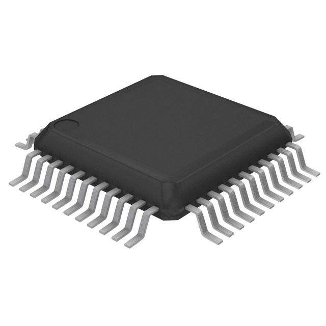
| 产品图片 |
|
| 产品型号 | LTC2612IMS8#PBF |
| rohs | 无铅 / 符合限制有害物质指令(RoHS)规范要求 |
| 产品系列 | - |
| 位数 | 14 |
| 供应商器件封装 | 8-MSOP |
| 包装 | 管件 |
| 安装类型 | 表面贴装 |
| 封装/外壳 | 8-TSSOP,8-MSOP(0.118",3.00mm 宽) |
| 工作温度 | -40°C ~ 85°C |
| 建立时间 | 9µs |
| 数据接口 | 串行 |
| 标准包装 | 50 |
| 电压源 | 单电源 |
| 转换器数 | 2 |
| 输出数和类型 | 2 电压,单极 |
| 采样率(每秒) | * |


- 商务部:美国ITC正式对集成电路等产品启动337调查
- 曝三星4nm工艺存在良率问题 高通将骁龙8 Gen1或转产台积电
- 太阳诱电将投资9.5亿元在常州建新厂生产MLCC 预计2023年完工
- 英特尔发布欧洲新工厂建设计划 深化IDM 2.0 战略
- 台积电先进制程称霸业界 有大客户加持明年业绩稳了
- 达到5530亿美元!SIA预计今年全球半导体销售额将创下新高
- 英特尔拟将自动驾驶子公司Mobileye上市 估值或超500亿美元
- 三星加码芯片和SET,合并消费电子和移动部门,撤换高东真等 CEO
- 三星电子宣布重大人事变动 还合并消费电子和移动部门
- 海关总署:前11个月进口集成电路产品价值2.52万亿元 增长14.8%


PDF Datasheet 数据手册内容提取
LTC2602/LTC2612/LTC2622 Dual 16-/14-/12-Bit Rail-to-Rail DACs in 8-Lead MSOP FEATURES DESCRIPTIOU ■ Smallest Pin-Compatible Dual DACs: The LTC®2602/LTC2612/LTC2622 are dual 16-,14- and LTC2602: 16-Bits 12-bit, 2.5V-to-5.5V rail-to-rail voltage-output DACs, in a LTC2612: 14-Bits tiny 8-lead MSOP package. They have built-in high per- LTC2622: 12-Bits formance output buffers and are guaranteed monotonic. ■ Guaranteed 16-Bit Monotonic Over Temperature These parts establish advanced performance standards ■ Wide 2.5V to 5.5V Supply Range for output drive, crosstalk and load regulation in single- ■ Low Power Operation: 300µA per DAC at 3V supply, voltage output multiples. ■ Individual Channel Power-Down to 1µA, Max ■ Ultralow Crosstalk between DACs (30µV) The parts use a simple SPI/MICROWIRE™ compatible ■ High Rail-to-Rail Output Drive (±15mA) 3-wire serial interface which can be operated at clock ■ Double-Buffered Data Latches rates up to 50MHz. ■ Pin-Compatible 10-Bit Version (LTC1661) The LTC2602/LTC2612/LTC2622 incorporate a power- ■ Tiny 8-Lead MSOP Package on reset circuit. During power-up, the voltage outputs APPLICATIOUS rise less than 10mV above zero scale, and after power- up, they stay at zero scale until a valid write and update ■ Mobile Communications take place. ■ Process Control and Industrial Automation , LTC and LT are registered trademarks of Linear Technology Corporation. All other trademarks are the property of their respective owners. ■ Instrumentation ■ Automatic Test Equipment BLOCK DIAGRAW LTC2602 Differential Nonlinearity (DNL)(LTC2602) 1.0 VOUT A 8 1D6A-CB IAT GISTER GISTER GISTER GISTER 1D6A-CB IBT 5 VOUT B 0.8 VVCRCEF = = 5 4V.096V RE RE RE RE 0.6 0.4 SB) 0.2 GND 7 6 VCC R (L 0 O R R–0.2 E CONTROL DECODE –0.4 LOGIC CS/LD 1 4 REF –0.6 –0.8 SCK 2 24-BIT SHIFT REGISTER 3 SDI –1.0 0 16384 32768 49152 65535 CODE 2602 BD01 2602 TA01 2602fa 1
LTC2602/LTC2612/LTC2622 ABSOLUTE WAXIWUW RATIUGS PACKAGE/ORDER IUFORWATIOU (Note 1) Any Pin to GND........................................... –0.3V to 6V Any Pin to VCC........................................................ –6V to 0.3V TOP VIEW Maximum Junction Temperature......................... 125°C CS/LD 1 8VOUT A SCK 2 7GND Operating Temperature Range SDI 3 6VCC REF 4 5VOUT B LTC2602C/LTC2612C/LTC2622C .......... 0°C to 70°C MS8 PACKAGE LTC2602I/LTC2612I/LTC2622I.......... –40°C to 85°C 8-LEAD PLASTIC MSOP Storage Temperature Range................ –65°C to 150°C TJMAX = 125°C, θJA = 300°C/W Lead Temperature (Soldering, 10 sec)................ 300°C ORDER PART NUMBER MS8 PART MARKING LTC2602CMS8 LTACX LTC2602IMS8 LTACY LTC2612CMS8 LTACZ LTC2612IMS8 LTADA LTC2622CMS8 LTADB LTC2622IMS8 LTADC Order Options Tape and Reel: Add #TR Lead Free: Add #PBF Lead Free Tape and Reel: Add #TRPBF Lead Free Part Marking: http://www.linear.com/leadfree/ Consult LTC Marketing for parts specified with wider operating temperature ranges. ELECTRICAL CHARACTERISTICS The ● denotes specifications which apply over the full operating temperature range, otherwise specifications are at TA = 25°C. VCC = 2.5V to 5.5V, VREF ≤ VCC, VOUT unloaded, unless otherwise noted. LTC2622 LTC2612 LTC2602 SYMBOL PARAMETER CONDITIONS MIN TYP MAX MIN TYP MAX MIN TYP MAX UNITS DC Performance Resolution ● 12 14 16 Bits Monotonicity V = 5V, V = 4.096V (Note 2) ● 12 14 16 Bits CC REF DNL Differential Nonlinearity VCC = 5V, VREF = 4.096V (Note 2) ● ±0.5 ±1 ±1 LSB INL Integral Nonlinearity VCC = 5V, VREF = 4.096V (Note 2) ● ±0.75 ±4 ±3 ±16 ±12 ±64 LSB Load Regulation V = V = 5V, Midscale REF CC I = 0mA to 15mA Sourcing ● 0.025 0.125 0.1 0.5 0.4 2 LSB/mA OUT I = 0mA to 15mA Sinking ● 0.05 0.125 0.2 0.5 0.65 2 LSB/mA OUT V = V = 2.5V, Midscale REF CC I = 0mA to 7.5mA Sourcing ● 0.05 0.25 0.2 1 0.9 4 LSB/mA OUT I = 0mA to 7.5mA Sinking ● 0.1 0.25 0.4 1 1.3 4 LSB/mA OUT ZSE Zero-Scale Error V = 5V, V = 4.096V Code = 0 ● 1 9 1 9 1 9 mV CC REF VOS Offset Error VCC = 5V, VREF = 4.096V (Note 7) ● ±1 ±9 ±1 ±9 ±1 ±9 mV VOS Temperature ±5 ±5 ±5 µV/°C Coefficient GE Gain Error VCC = 5V, VREF = 4.096V ● ±0.1 ±0.7 ±0.1 ±0.7 ±0.1 ±0.7 %FSR Gain Temperature ±3 ±3 ±3 ppm/°C Coefficient 2602fa 2
LTC2602/LTC2612/LTC2622 ELECTRICAL CHARACTERISTICS The ● denotes specifications which apply over the full operating temperature range, otherwise specifications are at TA = 25°C. VCC = 2.5V to 5.5V, VREF ≤ VCC, VOUT unloaded, unless otherwise noted. LTC2602/LTC2612/LTC2622 SYMBOL PARAMETER CONDITIONS MIN TYP MAX UNITS PSRR Power Supply Rejection Ratio VCC = 5V ±10% –80 dB ROUT DC Output Impedance VREF = VCC = 5V, Midscale; –15mA ≤ IOUT ≤ 15mA ● 0.05 0.15 Ω VREF = VCC = 2.5V, Midscale; –7.5mA ≤ IOUT ≤ 7.5mA ● 0.05 0.15 Ω DC Crosstalk (Note 4) Due to Full Scale Output Change (Note 5) ±30 µV Due to Load Current Change ±16 µV/mA Due to Powering Down (per Channel) ±4 µV I Short-Circuit Output Current V = 5.5V, V = 5.5V SC CC REF Code: Zero Scale; Forcing Output to V ● 15 34 60 mA CC Code: Full Scale; Forcing Output to GND ● 15 38 60 mA V = 2.5V, V = 2.5V CC REF Code: Zero Scale; Forcing Output to V ● 7.5 20 50 mA CC Code: Full Scale; Forcing Output to GND ● 7.5 28 50 mA Reference Input Input Voltage Range ● 0 V V CC Resistance Normal Mode ● 44 64 80 kΩ Capacitance 23 pF IREF Reference Current, Power Down Mode All DACs Powered Down ● 0.001 1 µA Power Supply V Positive Supply Voltage For Specified Performance ● 2.5 5.5 V CC I Supply Current V = 5V (Note 3) ● 0.7 1.3 mA CC CC V = 3V (Note 3) ● 0.6 1 mA CC All DACs Powered Down (Note 3) VCC = 5V ● 0.35 1 µA All DACs Powered Down (Note 3) VCC = 3V ● 0.10 1 µA Digital I/O V Digital Input High Voltage V = 2.5V to 5.5V ● 2.4 V IH CC V = 2.5V to 3.6V ● 2.0 V CC V Digital Input Low Voltage V = 4.5V to 5.5V ● 0.8 V IL CC V = 2.7V to 5.5V ● 0.6 V CC V = 2.5V to 5.5V ● 0.5 V CC ILK Digital Input Leakage VIN = GND to VCC ● ±1 µA C Digital Input Capacitance (Note 6) ● 8 pF IN LTC2622 LTC2612 LTC2602 SYMBOL PARAMETER CONDITIONS MIN TYP MAX MIN TYP MAX MIN TYP MAX UNITS AC Performance ts Settling Time (Note 8) ±0.024% (±1LSB at 12 Bits) 7 7 7 µs ±0.006% (±1LSB at 14 Bits) 9 9 µs ±0.0015% (±1LSB at 16 Bits) 10 µs Settling Time for ±0.024% (±1LSB at 12 Bits) 2.7 2.7 2.7 µs 1LSB Step (Note 9) ±0.006% (±1LSB at 14 Bits) 4.8 4.8 µs ±0.0015% (±1LSB at 16 Bits) 5.2 µs Voltage Output Slew Rate 0.80 0.80 0.80 V/µs Capacitive Load Driving 1000 1000 1000 pF Glitch Impulse At Midscale Transition 12 12 12 nV • s Multiplying Bandwidth 180 180 180 kHz en Output Voltage Noise At f = 1kHz 120 120 120 nV/√Hz Density At f = 10kHz 100 100 100 nV/√Hz Output Voltage Noise 0.1Hz to 10Hz 15 15 15 µVP-P 2602fa 3
LTC2602/LTC2612/LTC2622 TI W I U G CHARACTERISTICS The ● denotes specifications which apply over the full operating temperature range, otherwise specifications are at TA = 25°C. (See Figure 1) (Note 6) LTC2602/LTC2612/LTC2622 SYMBOL PARAMETER CONDITIONS MIN TYP MAX UNITS V = 2.5V to 5.5V CC t SDI Valid to SCK Setup ● 4 ns 1 t SDI Valid to SCK Hold ● 4 ns 2 t SCK High Time ● 9 ns 3 t SCK Low Time ● 9 ns 4 t CS/LD Pulse Width ● 10 ns 5 t LSB SCK High to CS/LD High ● 7 ns 6 t CS/LD Low to SCK High ● 7 ns 7 t CS/LD High to SCK Positive Edge ● 7 ns 10 SCK Frequency 50% Duty Cycle ● 50 MHz Note 1: Absolute maximum ratings are those values beyond which the life Note 5: RL = 2kΩ to GND or VCC at the output of the DAC not being tested. of a device may be impaired. Note 6: Guaranteed by design and not production tested. Note 2: Linearity and monotonicity are defined from code kL to code Note 7: Inferred from measurement at code 256 (LTC2602), code 64 2N – 1, where N is the resolution and kL is given by kL = 0.016(2N/VREF), (LTC2612) or code 16 (LTC2622), and at fullscale. rounded to the nearest whole code. For V = 4.096V and N = 16, k = REF L Note 8: V = 5V, V = 4.096V. DAC is stepped 1/4 scale to 3/4 scale CC REF 256 and linearity is defined from code 256 to code 65,535. and 3/4 scate to 1/4 scale. Load is 2k in parallel with 200pF to GND. Note 3: Digital inputs at 0V or V . CC Note 9: VCC = 5V, VREF = 4.096V. DAC is stepped ±LBS between half scale Note 4: DC crosstalk is measured with VCC = 5V and VREF = 4.096V, with and half scale –1. Load is 2k in parallel with 200pF to GND. the measured DAC at midscale, unless otherwise noted. TYPICAL PERFORW AU CE CHARACTERISTICS (LTC2602) Integral Nonlinearity (INL) Differential Nonlinearity (DNL) INL vs Temperature 32 1.0 32 VCC = 5V VCC = 5V 24 VREF = 4.096V 0.8 VREF = 4.096V 24 VCC = 5V 0.6 VREF = 4.096V 16 16 0.4 INL (LSB) –808 DNL (LSB)–00..202 INL (LSB) –808 INL (POS) –0.4 INL (NEG) –16 –16 –0.6 –24 –0.8 –24 –32 –1.0 –32 0 16384 32768 49152 65535 0 16384 32768 49152 65535 –50 –30 –10 10 30 50 70 90 CODE CODE TEMPERATURE (°C) 2602 G20 2602 G21 2602 G22 2602fa 4
LTC2602/LTC2612/LTC2622 TYPICAL PERFORW AU CE CHARACTERISTICS (LTC2602) DNL vs Temperature INL vs V DNL vs V REF REF 1.0 32 1.5 0.8 VCC = 5V 24 VCC = 5.5V VCC = 5.5V VREF = 4.096V 1.0 0.6 16 0.4 DNL (POS) INL (POS) 0.5 8 DNL (LSB)–00..202 DNL (NEG) INL (LSB) –08 INL (NEG) DNL (LSB)–0.05 DDNNLL ((PNOEGS)) –0.4 –16 –0.6 –1.0 –24 –0.8 –1.0 –32 –1.5 –50 –30 –10 10 30 50 70 90 0 1 2 3 4 5 0 1 2 3 4 5 TEMPERATURE (°C) VREF (V) VREF (V) 2602 G23 2602 G24 2602 G25 Settling to ±1LSB Settling of Full-Scale Step VOUT VOUT 100µV/DIV 100µV/DIV 12.3µs 9.7µs CS/LD CS/LD 2V/DIV 2V/DIV 2µs/DIV 2602 G26 5µs/DIV 2602 G27 VCC = 5V, VREF = 4.096V VCC = 5V, VREF = 4.096V 1/4-SCALE TO 3/4-SCALE STEP CODE 512 TO 65535 STEP RL = 2k, CL = 200pF AVERAGE OF 2048 EVENTS AVERAGE OF 2048 EVENTS SETTLING TO ±1LSB (LTC2612) Integral Nonlinearity (INL) Differential Nonlinearity (DNL) Settling to ±1LSB 8 1.0 VCC = 5V VCC = 5V 6 VREF = 4.096V 0.8 VREF = 4.096V 0.6 4 0.4 2 VOUT B) B) 0.2 100µV/DIV S S L (L 0 L (L 0 IN –2 DN–0.2 2CVS/D/LIDV 8.9µs –0.4 –4 –0.6 2µs/DIV 2602 G30 –6 –0.8 VCC = 5V, VREF = 4.096V 1/4-SCALE TO 3/4-SCALE STEP –8 –1.0 0 4096 8192 12288 16383 0 4096 8192 12288 16383 RL = 2k, CL = 200pF AVERAGE OF 2048 EVENTS CODE CODE 2602 G28 2602 G29 2602fa 5
LTC2602/LTC2612/LTC2622 TYPICAL PERFORW AU CE CHARACTERISTICS (LTC2622) Integral Nonlinearity (INL) Differential Nonlinearity (DNL) Settling to ±1LSB 2.0 1.0 VCC = 5V VCC = 5V 1.5 VREF = 4.096V 0.8 VREF = 4.096V 0.6 1.0 6.8µs 0.4 VOUT INL (LSB)–00..505 DNL (LSB) –00..202 1m2CVVS//DD/LIIDVV –0.4 –1.0 –0.6 2µs/DIV 2602 G33 –1.5 –0.8 VCC = 5V, VREF = 4.096V 1/4-SCALE TO 3/4-SCALE STEP –2.00 1024 2048 3072 4095 –1.00 1024 2048 3072 4095 RL = 2k, CL = 200pF AVERAGE OF 2048 EVENTS CODE CODE 2602 G31 2602 G32 (LTC2602/LTC2612/LTC2622) Current Limiting Load Regulation Offset Error vs Temperature 0.10 1.0 3 CODE = MIDSCALE CODE = MIDSCALE 0.08 0.8 VREF = VCC = 5V 2 0.06 0.6 VREF = VCC = 3V 0.04 0.4 mV) 1 V (V)∆OUT––000...0002024 VREF = VCC = 3V V (mV)∆OUT ––000...2024 VREF = VCC = 5V OFFSET ERROR ( –01 VREF = VCC = 5V VREF = VCC = 3V –0.06 –0.6 –2 –0.08 –0.8 –0.10 –1.0 –3 –40 –30 –20 –10 0 10 20 30 40 –35 –25 –15 –5 5 15 25 35 –50 –30 –10 10 30 50 70 90 IOUT (mA) IOUT (mA) TEMPERATURE (°C) 2602 G01 2602 G02 2602 G03 Zero-Scale Error vs Temperature Gain Error vs Temperature Offset Error vs V CC 3 0.4 3 0.3 2.5 2 V) 0.2 SCALE ERROR (m 21..05 N ERROR (%FSR)–00..101 SET ERROR (mV) 10 O- 1.0 AI FF –1 R G O E –0.2 Z 0.5 –2 –0.3 0 –0.4 –3 –50 –30 –10 10 30 50 70 90 –50 –30 –10 10 30 50 70 90 2.5 3 3.5 4 4.5 5 5.5 TEMPERATURE (°C) TEMPERATURE (°C) VCC (V) 2602 G04 2602 G05 2602 G06 2602fa 6
LTC2602/LTC2612/LTC2622 TYPICAL PERFORW AU CE CHARACTERISTICS (LTC2602/LTC2612/LTC2622) Gain Error vs V I Shutdown vs V Large-Signal Settling CC CC CC 0.4 450 0.3 400 0.2 350 %FSR) 0.1 300 VOUT R ( 0 nA)250 0.5V/DIV ERRO–0.1 I (CC200 AIN 150 VREF = VCC = 5V G–0.2 1/4-SCALE TO 3/4-SCALE 100 –0.3 50 2.5µs/DIV 2602 G09 –0.4 0 2.5 3 3.5 4 4.5 5 5.5 2.5 3 3.5 4 4.5 5 5.5 VCC (V) VCC (V) 2602 G07 2602 G08 Headroom at Rails vs Output Midscale Glitch Impulse Power-On Reset Glitch Current 5.0 4.5 5V SOURCING 4.0 10mVV/ODUIVT VCC 3.5 1V/DIV 3V SOURCING 12nV-s TYP 3.0 V) 44mmVV P PEEAAKK (OUT 2.5 CS/LD V 2.0 5V/DIV VOUT 1.5 10mV/DIV 5V SINKING 1.0 2.5µs/DIV 2602 G10 250µs/DIV 2602 G11 3V SINKING 0.5 0 0 1 2 3 4 5 6 7 8 9 10 IOUT (mA) 2602 G12 Supply Current vs Logic Voltage Exiting Power-Down to Midscale Multiplying Frequency Response 1.6 0 VCC = 5V VCC = 5V –3 1.4 SAWNDE ECPS /SLCDK, SDI VREF = 2V –6 1.2 0V TO VCC VOUT –9 0.5V/DIV –12 A) 1.0 –15 (mCC 0.8 OPONWE DERA CD IONWN MODE dB––1281 I CS/LD 5V/DIV –24 0.6 VCC = 5V –27 VREF (DC) = 2V 0.4 2.5µs/DIV 2602 G14 –30 VCROEDFE ( A=C F)U =L L0 .S2CVAP-LPE –33 0.2 –36 0 0.5 1 1.5 2 2.5 3 3.5 4 4.5 5 1k 10k 100k 1M LOGIC VOLTAGE (V) FREQUENCY (Hz) 2602 G16 2602 G13 2602fa 7
LTC2602/LTC2612/LTC2622 TYPICAL PERFORW AU CE CHARACTERISTICS (LTC2602/LTC2612/LTC2622) Output Voltage Noise, Short-Circuit Output Current vs Short-Circuit Output Current vs 0.1Hz to 10Hz V (Sinking) V (Sourcing) OUT OUT 50 0 VCC = 5.5V VCC = 5.5V VREF = 5.6V VREF = 5.6V 40 CODE = 0 –10 CODE = FULL SCALE VOUT SWEPT 0V TO VCC VOUT SWEPT VCC TO 0V VOUT V 30 V –20 10µV/DIV DI DI A/ A/ m m 0 0 1 20 1 –30 10 –40 0 1 2 3 4 5 6 7 8 9 10 SECONDS 0 –50 2602 G17 0 1 2 3 4 5 6 0 1 2 3 4 5 6 1V/DIV 1V/DIV 2602 G34 2602 G35 2602fa 8
LTC2602/LTC2612/LTC2622 PIUN FUUNCTIOUNS CS/LD (Pin 1): Serial Interface Chip Select/Load Input. LTC2602/LTC2612/LTC2622 accept input word lengths When CS/LD is low, SCK is enabled for shifting data on SDI of either 24 or 32 bits. into the register. When CS/LD is taken high, SCK is dis- REF (Pin 4): Reference Voltage Input. 0V ≤ V ≤ V . REF CC abled and the specified command (see Table 1) is ex- ecuted. VOUT B and VOUT A (Pins 5 and 8): DAC Analog Voltage Outputs. The output range is 0 – V . REF SCK (Pin 2): Serial Interface Clock Input. CMOS and TTL compatible. VCC (Pin 6): Supply Voltage Input. 2.5V ≤ VCC ≤ 5.5V. SDI (Pin 3): Serial Interface Data Input. Data is applied to GND (Pin 7): Analog Ground. SDI for transfer to the device at the rising edge of SCK. The BLOCK DIAGRAW R R R R VOUT A 8 DAC A DACGISTE NPUTGISTE NPUTGISTE DACGISTE DAC B 5 VOUT B E IE IE E R R R R GND 7 6 VCC CONTROL DECODE LOGIC CS/LD 1 4 REF SCK 2 24-BIT SHIFT REGISTER 3 SDI 2602 BD TI W I U G DIAGRAW t1 t2 t3 t4 t6 SCK 1 2 3 23 24 t10 SDI C3 C2 C1 D1 D0 t5 t7 CS/LD 2602 F01 Figure 1 2602fa 9
LTC2602/LTC2612/LTC2622 OPERATIOU Power-On Reset The LTC2602/LTC2612/LTC2622 clear the outputs to zero Serial Interface scale when power is first applied, making system initializa- The CS/LD input is level triggered. When this input is taken tion consistent and repeatable. low, it acts as a chip-select signal, activating the SDI and For some applications, downstream circuits are active SCK buffers and enabling the input shift register. Data during DAC power-up, and may be sensitive to nonzero (SDI input) is transferred at the next 24 rising SCK edges. outputs from the DAC during this time. The LTC2602/ The 4-bit command, C3-C0, is loaded first; then the 4-bit LTC2612/LTC2622 contain circuitry to reduce the power- DAC address, A3-A0; and finally the 16-bit data word. The on glitch; furthermore, the glitch amplitude can be made data word comprises the 16-, 14- or 12-bit input code, smaller by reducing the ramp rate of the power supply. For ordered MSB-to-LSB, followed by 0, 2 or 4 don’t-care bits example, if the power supply is ramped to 5V in 1ms, the (LTC2602, LTC2612 and LTC2622 respectively). Data can analog outputs rise less than 10mV above ground (typ) during power-on. See Power-On Reset Glitch in the Typi- only be transferred to the device when the CS/LD signal is cal Performance Characteristics section. low.The rising edge of CS/LD ends the data transfer and causes the device to carry out the action specified in the Power Supply Sequencing 24-bit input word. The complete sequence is shown in Figure 2a. The voltage at REF (Pin 4) should be kept within the range –0.3V ≤ VREF ≤ VCC + 0.3V (see Absolute Maximum The command (C3-C0) and address (A3-A0) assignments Ratings). Particular care should be taken to observe these are shown in Table 1. The first four commands in the table limits during power supply turn-on and turn-off sequences, consist of write and update operations. A write operation when the voltage at V (Pin 6) is in transition. CC loads a 16-bit data word from the 32-bit shift register into the input register of the selected DAC, n. An update Transfer Function operation copies the data word from the input register to The digital-to-analog transfer function is the DAC register. Once copied into the DAC register, the data word becomes the active 16-, 14- or 12-bit input ⎛ k ⎞ VOUT(IDEAL) =⎜ ⎟VREF code, and is converted to an analog voltage at the DAC ⎝2N⎠ output. The update operation also powers up the selected where k is the decimal equivalent of the binary DAC input DAC if it had been in power-down mode. The data path and code, N is the resolution and V is the voltage at REF REF registers are shown in the block diagram. (Pin 4). While the minimum input word is 24 bits, it may optionally Table 1. be extended to 32 bits to accommodate microprocessors COMMAND* which have a minimum word width of 16 bits (2 bytes). To C3 C2 C1 C0 use the 32-bit word width, 8 don’t-care bits are transferred 0 0 0 0 Write to Input Register n to the device first, followed by the 24-bit word as just 0 0 0 1 Update (Power Up) DAC Register n described. Figure 2b shows the 32-bit sequence. 0 0 1 0 Write to Input Register n, Update (Power Up) All n 0 0 1 1 Write to and Update (Power Up) n Power-Down Mode 0 1 0 0 Power Down n 1 1 1 1 No Operation For power-constrained applications, power-down mode ADDRESS (n)* can be used to reduce the supply current whenever less A3 A2 A1 A0 than two outputs are needed. When in power-down, the 0 0 0 0 DAC A buffer amplifiers, bias circuits and reference inputs are 0 0 0 1 DAC B disabled, and draw essentially zero current. The DAC 1 1 1 1 All DACs outputs are put into a high-impedance state, and the *Command and address codes not shown are reserved and should not be used. 2602fa 10
LTC2602/LTC2612/LTC2622 OPERATIOU INPUT WORD (LTC2602) COMMAND ADDRESS DATA (16 BITS) C3 C2 C1 C0 A3 A2 A1 A0 D15 D14 D13 D12 D11 D10 D9 D8 D7 D6 D5 D4 D3 D2 D1 D0 MSB LSB 2602 TBL01 INPUT WORD (LTC2612) COMMAND ADDRESS DATA (14 BITS + 2 DON’T-CARE BITS) C3 C2 C1 C0 A3 A2 A1 A0 D13 D12 D11 D10 D9 D8 D7 D6 D5 D4 D3 D2 D1 D0 X X MSB LSB 2602 TBL02 INPUT WORD (LTC2622) COMMAND ADDRESS DATA (12 BITS + 4 DON’T-CARE BITS) C3 C2 C1 C0 A3 A2 A1 A0 D11 D10 D9 D8 D7 D6 D5 D4 D3 D2 D1 D0 X X X X MSB LSB 2602 TBL03 output pins are passively pulled to ground through indi- Voltage Outputs vidual 90kΩ resistors. Input- and DAC-register contents Each of the two rail-to-rail amplifiers contained in these are not disturbed during power-down. parts has guaranteed load regulation when sourcing or Either channel or both channels can be put into power- sinking up to 15mA at 5V (7.5mA at 3V). down mode by using command 0100 in combination with b Load regulation is a measure of the amplifier’s ability to the appropriate DAC address, (n). The 16-bit data word is maintain the rated voltage accuracy over a wide range of ignored. The supply and reference currents are reduced by load conditions. The measured change in output voltage approximately 50% for each DAC powered down; the per milliampere of forced load current change is ex- effective resistance at REF (pin 4) rises accordingly, pressed in LSB/mA. becoming a high-impedance input (typically > 1GΩ) when both DACs are powered down. DC output impedance is equivalent to load regulation, and may be derived from it by simply calculating a change in Normal operation can be resumed by executing any com- units from LSB/mA to Ohms. The amplifiers’ DC output mand which includes a DAC update, as shown in Table 1. impedance is 0.050Ω when driving a load well away from The selected DAC is powered up as its voltage output is the rails. updated. When a DAC which is in a powered-down state is powered up and updated, normal settling is delayed. If one When drawing a load current from either rail, the output of the two DACs is in a powered-down state prior to the voltage headroom with respect to that rail is limited by the update command, the power-up delay is 5µs. If, on the 25Ω typical channel resistance of the output devices; e.g., other hand, both DACs are powered down, then the main when sinking 1mA, the minimum output voltage = 25Ω • bias generation circuit block has been automatically shut 1mA = 25mV. See the graph Headroom at Rails vs Output down in addition to the individual DAC amplifiers and Current in the Typical Performance Characteristics sec- reference inputs. In this case, the power up delay time is tion. 12µs (for VCC = 5V) or 30µs (for VCC = 3V). The amplifiers are stable driving capacitive loads of up to 1000pF. 2602fa 11
LTC2602/LTC2612/LTC2622 OPERATIOU Board Layout The GND pin of the part should be connected to analog ground. Resistance from the GND pin to system star The excellent load regulation and DC crosstalk perfor- ground should be as low as possible. Resistance here will mance of these devices is achieved in part by keeping add directly to the effective DC output impedance of the “signal” and “power” grounds separated internally and by device (typically 0.050Ω), and will degrade DC crosstalk. reducing shared internal resistance. Note that the LTC2602/LTC2612/LTC2622 are no more The GND pin functions both as the node to which the susceptible to these effects than other parts of their type; reference and output voltages are referred and as a return on the contrary, they allow layout-based performance path for power currents in the device. Because of this, improvements to shine rather than limiting attainable careful thought should be given to the grounding scheme performance with excessive internal resistance. and board layout in order to ensure rated performance. Rail-to-Rail Output Considerations The PC board should have separate areas for the analog and digital sections of the circuit. This keeps digital signals In any rail-to-rail voltage output device, the output is away from sensitive analog signals and facilitates the use limited to voltages within the supply range. of separate digital and analog ground planes which have Since the analog outputs of the device cannot go below minimal capacitive and resistive interaction with each ground, they may limit for the lowest codes as shown in other. Figure 3b. Similarly, limiting can occur near full scale Digital and analog ground planes should be joined at only when the REF pin is tied to V . If V = V and the DAC CC REF CC one point, establishing a system star ground as close to full-scale error (FSE) is positive, the output for the highest the device’s ground pin as possible. Ideally, the analog codes limits at V as shown in Figure 3c. No full-scale CC ground plane should be located on the component side of limiting can occur if V is less than V – FSE. REF CC the board, and should be allowed to run under the part to Offset and linearity are defined and tested over the region shield it from noise. Analog ground should be a continu- of the DAC transfer function where no output limiting can ous and uninterrupted plane, except for necessary lead occur. pads and vias, with signal traces on another layer. 2602fa 12
LTC2602/LTC2612/LTC2622 OPERATIOU 2602 F02b 2 3 0 D 1 3 1 D 0 3 2 D YYYY F02a 29 D3 8 4 2 4 2 0 D D 7 23 1 2 D5 D 6 2 2 6 2 2 D D 21 3 25 D7 ORD D W 20 D4 24 D8 DATA 3 9 2 9 1 5 D D ) 18 D6 Wordss 22 D10 BitsBits 568159161110127131417 A3A2A1A0D15D14D13D12D11D10D9D8D7 ADDRESS WORDDATA WORD 24-BIT INPUT WORD Figure 2a. LTC2602 24-Bit Load Sequence (Minimum Input LTC2612 SDI Data Word 14-Bit Input Code + 2 Don’t Care BitLTC2622 SDI Data Word 12-Bit Input Code + 4 Don’t Care Bit 1591916201118101221131417 CC32C1C0A3A2A1A0D15D14D13D12D11 COMMAND WORDADDRESS WORD Figure 2b. LTC2602 32-Bit Load SequenceLTC2612 SDI Data Word 14-Bit Input Code + 2 Don’t Care LTC2622 SDI Data Word 12-Bit Input Code + 4 Don’t Care 8 4 0 X C D R 7 3 1 WO X C D N 6 2 2 MA X C M 1 C3 CO 5 X CARE T 4 N’ X O D 3 S/LD SCK SDI X C 2 X 1 X S/LD SCK SDI C 2602fa 13
LTC2602/LTC2612/LTC2622 OPERATIOU POSITIVE VREF = VCC FSE VREF = VCC OUTPUT VOLTAGE OUTPUT VOLTAGE INPUT CODE OUTPUT (c) VOLTAGE 0 32,768 65,535 INPUT CODE 0V NEGATIVE INPUT CODE (a) OFFSET 2600 F03 (b) Figure 3. Effects of Rail-to-Rail Operation On a DAC Transfer Curve. (a) Overall Transfer Function (b) Effect of Negative Offset for Codes Near Zero Scale (c) Effect of Positive Full-Scale Error for Codes Near Full Scale 2602fa 14
LTC2602/LTC2612/LTC2622 PACKAGE DESCRIPTIOU MS8 Package 8-Lead Plastic MSOP (Reference LTC DWG # 05-08-1660) 0.889 ± 0.127 (.035 ± .005) 5.23 3.20 – 3.45 (.206) (.126 – .136) MIN 3.00 ± 0.102 0.42 ± 0.038 0.65 (.118 ± .004) 0.52 (.0165 ± .0015) (.0256) (NOTE 3) 8 7 6 5 (.0205) TYP BSC REF RECOMMENDED SOLDER PAD LAYOUT 3.00 ± 0.102 4.90 ± 0.152 DETAIL “A” (.118 ± .004) 0.254 (.193 ± .006) (NOTE 4) (.010) 0° – 6° TYP GAUGE PLANE 1 2 3 4 0.53 ± 0.152 (.021 ± .006) 1.10 0.86 (.043) (.034) DETAIL “A” MAX REF 0.18 (.007) SEATING PLANE 0.22 – 0.38 0.127 ± 0.076 (.009 – .015) (.005 ± .003) 0.65 TYP MSOP (MS8) 0603 (.0256) NOTE: BSC 1. DIMENSIONS IN MILLIMETER/(INCH) 2. DRAWING NOT TO SCALE 3. DIMENSION DOES NOT INCLUDE MOLD FLASH, PROTRUSIONS OR GATE BURRS. MOLD FLASH, PROTRUSIONS OR GATE BURRS SHALL NOT EXCEED 0.152mm (.006") PER SIDE 4. DIMENSION DOES NOT INCLUDE INTERLEAD FLASH OR PROTRUSIONS. INTERLEAD FLASH OR PROTRUSIONS SHALL NOT EXCEED 0.152mm (.006") PER SIDE 5. LEAD COPLANARITY (BOTTOM OF LEADS AFTER FORMING) SHALL BE 0.102mm (.004") MAX 2602fa Information furnished by Linear Technology Corporation is believed to be accurate and reliable. 15 However, no responsibility is assumed for its use. Linear Technology Corporation makes no represen- tation that the interconnection of its circuits as described herein will not infringe on existing patent rights.
LTC2602/LTC2612/LTC2622 RELATED PARTS PART NUMBER DESCRIPTION COMMENTS LTC1458/LTC1458L Quad 12-Bit Rail-to-Rail Output DACs with Added Functionality LTC1458: V = 4.5V to 5.5V, V = 0V to 4.096V CC OUT LTC1458L: V = 2.7V to 5.5V, V = 0V to 2.5V CC OUT LTC1654 Dual 14-Bit Rail-to-Rail VOUT DAC Programmable Speed/Power, 3.5µs/750µA, 8µs/450µA LTC1655/LTC1655L Single 16-Bit V DAC with Serial Interface in SO-8 V = 5V(3V), Low Power, Deglitched OUT CC LTC1657/LTC1657L Parrallel 5V/3V 16-Bit V DAC Low Power, Deglitched, Rail-to-Rail V OUT OUT LTC1660/LTC1665 Octal 10/8-Bit V DAC in 16-Pin Narrow SSOP V = 2.7V to 5.5V, Micropower, Rail-to-Rail Output OUT CC LTC1661 Dual 10-Bit VOUT DAC in 8-Lead MSOP Package VCC = 2.7V to 5.5V, 60µA per DAC, Rail-to-Rail Output LTC1821 Parallel 16-Bit Voltage Output DAC Precision 16-Bit Settling in 2µs for 10V Step LTC2600/LTC2610/ Octal 16/14/12-Bit Rail-to-Rail DACs in 16-Lead SSOP 250µA per DAC, 2.5V to 5.5V Supply Range LTC2620 Rail-to-Rail Output 2602fa 16 Linear Technology Corporation RD/LT 1205 REV A • PRINTED IN THE USA 1630 McCarthy Blvd., Milpitas, CA 95035-7417 (408) 432-1900 ● FAX: (408) 434-0507 ● www.linear.com © LINEAR TECHNOLOGY CORPORATION 2003