ICGOO在线商城 > 集成电路(IC) > 数据采集 - 数模转换器 > AD9754ARZ
 Datasheet下载
- 型号: AD9754ARZ
- 制造商: Analog
- 库位|库存: xxxx|xxxx
- 要求:
| 数量阶梯 | 香港交货 | 国内含税 |
| +xxxx | $xxxx | ¥xxxx |
查看当月历史价格
查看今年历史价格
AD9754ARZ产品简介:
ICGOO电子元器件商城为您提供AD9754ARZ由Analog设计生产,在icgoo商城现货销售,并且可以通过原厂、代理商等渠道进行代购。 AD9754ARZ价格参考¥100.42-¥139.44。AnalogAD9754ARZ封装/规格:数据采集 - 数模转换器, 14 位 数模转换器 1 28-SOIC。您可以下载AD9754ARZ参考资料、Datasheet数据手册功能说明书,资料中有AD9754ARZ 详细功能的应用电路图电压和使用方法及教程。
AD9754ARZ是由Analog Devices Inc.(ADI)公司生产的一款数模转换器(DAC),广泛应用于需要高性能信号生成的场合。该器件具有14位分辨率,支持高速转换,适用于通信系统、测试测量设备、工业控制以及医疗成像设备等领域。

在通信领域,AD9754ARZ常用于无线基站、软件无线电(SDR)系统中,将数字信号转换为模拟射频或中频信号进行传输。其高精度和高速特性使其能够满足现代通信对信号质量和带宽的要求。

在测试与测量设备中,如信号发生器、频谱分析仪等,AD9754ARZ用于生成高保真模拟信号,以测试其他设备的性能。其优异的动态性能(如低谐波失真和高无杂散动态范围)确保了测试结果的准确性。

此外,AD9754ARZ还适用于工业自动化系统中的精密控制,以及超声波成像、CT扫描等医疗设备中的信号处理模块,提供稳定可靠的模拟输出。

总之,AD9754ARZ凭借其高分辨率、高速度和良好的线性度,广泛应用于对信号质量要求较高的高性能电子系统中。
| 参数 | 数值 |
| 产品目录 | 集成电路 (IC)半导体 |
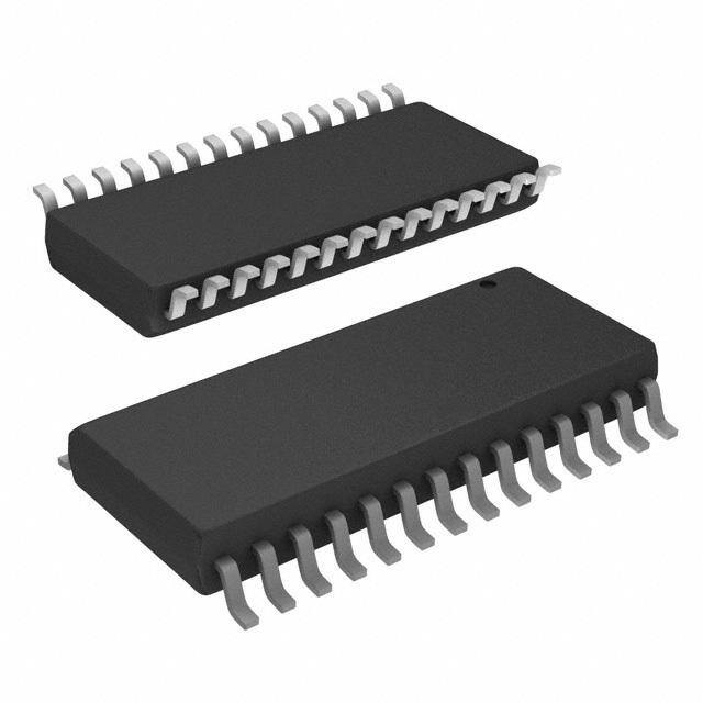
| 描述 | IC DAC 14BIT 125MSPS 28-SOIC数模转换器- DAC 14-Bit 100 MSPS |
| DevelopmentKit | AD9754-EBZ |
| 产品分类 | |
| 品牌 | Analog Devices |
| 产品手册 | |
| 产品图片 |
|
| rohs | 符合RoHS无铅 / 符合限制有害物质指令(RoHS)规范要求 |
| 产品系列 | 数据转换器IC,数模转换器- DAC,Analog Devices AD9754ARZTxDAC® |
| 数据手册 | |
| 产品型号 | AD9754ARZ |
| PCN组件/产地 | |
| 产品培训模块 | http://www.digikey.cn/PTM/IndividualPTM.page?site=cn&lang=zhs&ptm=19145http://www.digikey.cn/PTM/IndividualPTM.page?site=cn&lang=zhs&ptm=18614http://www.digikey.cn/PTM/IndividualPTM.page?site=cn&lang=zhs&ptm=26125http://www.digikey.cn/PTM/IndividualPTM.page?site=cn&lang=zhs&ptm=26140http://www.digikey.cn/PTM/IndividualPTM.page?site=cn&lang=zhs&ptm=26150http://www.digikey.cn/PTM/IndividualPTM.page?site=cn&lang=zhs&ptm=26147 |
| 产品目录页面 | |
| 产品种类 | 数模转换器- DAC |
| 位数 | 14 |
| 供应商器件封装 | 28-SOIC W |
| 分辨率 | 14 bit |
| 包装 | 管件 |
| 商标 | Analog Devices |
| 安装类型 | 表面贴装 |
| 安装风格 | SMD/SMT |
| 封装 | Tube |
| 封装/外壳 | 28-SOIC(0.295",7.50mm 宽) |
| 封装/箱体 | SOIC-28 |
| 工作温度 | -40°C ~ 85°C |
| 工厂包装数量 | 27 |
| 建立时间 | 35ns |
| 接口类型 | Parallel |
| 数据接口 | 并联 |
| 最大功率耗散 | 220 mW |
| 最大工作温度 | + 85 C |
| 最小工作温度 | - 40 C |
| 标准包装 | 27 |
| 电压参考 | Internal, External |
| 电压源 | 模拟和数字 |
| 电源电压-最大 | 5.5 V |
| 电源电压-最小 | 4.5 V |
| 积分非线性 | +/- 3 LSB |
| 稳定时间 | 35 ns |
| 系列 | AD9754 |
| 转换器数 | 1 |
| 转换器数量 | 1 |
| 输出数和类型 | 1 电流,单极1 电流,双极 |
| 输出类型 | Current |
| 采样比 | 125 MSPs |
| 采样率(每秒) | 125M |


- 商务部:美国ITC正式对集成电路等产品启动337调查
- 曝三星4nm工艺存在良率问题 高通将骁龙8 Gen1或转产台积电
- 太阳诱电将投资9.5亿元在常州建新厂生产MLCC 预计2023年完工
- 英特尔发布欧洲新工厂建设计划 深化IDM 2.0 战略
- 台积电先进制程称霸业界 有大客户加持明年业绩稳了
- 达到5530亿美元!SIA预计今年全球半导体销售额将创下新高
- 英特尔拟将自动驾驶子公司Mobileye上市 估值或超500亿美元
- 三星加码芯片和SET,合并消费电子和移动部门,撤换高东真等 CEO
- 三星电子宣布重大人事变动 还合并消费电子和移动部门
- 海关总署:前11个月进口集成电路产品价值2.52万亿元 增长14.8%


PDF Datasheet 数据手册内容提取
a 14-Bit, 125 MSPS High Performance TxDAC® D/A Converter AD9754* FEATURES FUNCTIONAL BLOCK DIAGRAM High Performance Member of Pin-Compatible +5V TxDAC Product Family 125 MSPS Update Rate REFLO 150pF AVDD ACOM 14-Bit Resolution 0.1mF +1.20V REF AD9754 Excellent Spurious Free Dynamic Range Performance REFIO CURRENT ICOMP 0.1mF FS ADJ SOURCE SFDR to Nyquist @ 5 MHz Output: 83 dBc ARRAY Differential Current Outputs: 2 mA to 20 mA RSET +5V DVDD IOUTA SEGMENTED LSB Power Dissipation: 185 mW @ 5V DCOM SWITCHES SWITCHES IOUTB Power-Down Mode: 20 mW @ 5V CLOCK CLOCK LATCHES On-Chip 1.20 V Reference SLEEP CMOS-Compatible +2.7 V to +5.5 V Digital Interface DIGITAL DATA INPUTS (DB13–DB0) Package: 28-Lead SOIC, TSSOP Packages The AD9754 is a current-output DAC with a nominal full-scale Edge-Triggered Latches output current of 20 mA and > 100 kW output impedance. APPLICATIONS Differential current outputs are provided to support single- Wideband Communication Transmit Channel: ended or differential applications. Matching between the two Direct IF current outputs ensures enhanced dynamic performance in a Basestations differential output configuration. The current outputs may be Wireless Local Loop tied directly to an output resistor to provide two complemen- Digital Radio Link tary, single-ended voltage outputs or fed directly into a trans- Direct Digital Synthesis (DDS) former. The output voltage compliance range is 1.25V. Instrumentation The on-chip reference and control amplifier are configured for PRODUCT DESCRIPTION maximum accuracy and flexibility. The AD9754 can be driven The AD9754 is a 14-bit resolution, wideband, second genera- by the on-chip reference or by a variety of external reference tion member of the TxDAC series of high performance, low voltages. The internal control amplifier, which provides a wide power CMOS digital-to-analog-converters (DACs). The TxDAC family, which consists of pin compatible 8-, 10-, 12- (>10:1) adjustment span, allows the AD9754 full-scale current to be adjusted over a 2mA to 20 mA range while maintaining and 14-bit DACs, is specifically optimized for the transmit excellent dynamic performance. Thus, the AD9754 may operate signal path of communication systems. All of the devices share at reduced power levels or be adjusted over a 20dB range to the same interface options, small outline package and pinout, provide additional gain ranging capabilities. providing an upward or downward component selection path based on performance, resolution and cost. The AD9754 offers The AD9754 is available in 28-lead SOIC and TSSOP packages. exceptional ac and dc performance while supporting update It is specified for operation over the industrial temperature range. rates up to 125 MSPS. PRODUCT HIGHLIGHTS The AD9754’s flexible single-supply operating range of +4.5 V to 1. The AD9754 is a member of the wideband TxDAC high per- +5.5 V and low power dissipation are well suited for portable and formance product family that provides an upward or downward low power applications. Its power dissipation can be further reduc- component selection path based on resolution (8 to 14 bits), ed to a mere 65 mW with a slight degradation in performance by performance and cost. The entire family of TxDACs is avail- lowering the full-scale current output. Also, a power-down mode able in industry standard pinouts. reduces the standby power dissipation to approximately 20mW. 2. Manufactured on a CMOS process, the AD9754 uses a The AD9754 is manufactured on an advanced CMOS process. proprietary switching technique that enhances dynamic per- A segmented current source architecture is combined with a formance beyond that previously attainable by higher power/ proprietary switching technique to reduce spurious components cost bipolar or BiCMOS devices. and enhance dynamic performance. Edge-triggered input latches 3. On-chip, edge-triggered input CMOS latches readily inter- and a 1.2 V temperature compensated bandgap reference have face to +2.7 V to +5 V CMOS logic families. The AD9754 been integrated to provide a complete monolithic DAC solution. can support update rates up to 125 MSPS. The digital inputs support +2.7 V and +5 V CMOS logic families. 4. A flexible single-supply operating range of +4.5V to +5.5 V, TxDAC is a registered trademark of Analog Devices, Inc. and a wide full-scale current adjustment span of 2mA to *Protected by U.S. Patents Numbers 5450084, 5568145, 5689257, 5612697 and 20 mA, allows the AD9754 to operate at reduced power levels. 5703519. REV.A 5. The current output(s) of the AD9754 can be easily config- ured for various single-ended or differential circuit topologies. Information furnished by Analog Devices is believed to be accurate and reliable. However, no responsibility is assumed by Analog Devices for its use, nor for any infringements of patents or other rights of third parties One Technology Way, P.O. Box 9106, Norwood, MA 02062-9106,U.S.A. which may result from its use. No license is granted by implication or Tel: 781/329-4700 World Wide Web Site: http://www.analog.com otherwise under any patent or patent rights of Analog Devices. Fax: 781/326-8703 © Analog Devices, Inc., 1999
AD9754–SPECIFICATIONS DC SPECIFICATIONS (T to T , AVDD = +5 V, DVDD = +5 V, I = 20 mA, unless otherwise noted) MIN MAX OUTFS Parameter Min Typ Max Units RESOLUTION 14 Bits DC ACCURACY1 Integral Linearity Error (INL) T = +25(cid:176) C –3.0 – 1.5 +3.0 LSB A Differential Nonlinearity (DNL) T = +25(cid:176) C –2.0 – 0.75 +2.0 LSB A ANALOG OUTPUT Offset Error –0.02 +0.02 % of FSR Gain Error (Without Internal Reference) –2 – 0.5 +2 % of FSR Gain Error (With Internal Reference) –5 – 1.5 +5 % of FSR Full-Scale Output Current2 2.0 20.0 mA Output Compliance Range –1.0 1.25 V Output Resistance 100 kW Output Capacitance 5 pF REFERENCE OUTPUT Reference Voltage 1.14 1.20 1.26 V Reference Output Current3 100 nA REFERENCE INPUT Input Compliance Range 0.1 1.25 V Reference Input Resistance 1 MW Small Signal Bandwidth 0.5 MHz TEMPERATURE COEFFICIENTS Offset Drift 0 ppm of FSR/(cid:176) C Gain Drift (Without Internal Reference) – 50 ppm of FSR/(cid:176) C Gain Drift (With Internal Reference) – 100 ppm of FSR/(cid:176) C Reference Voltage Drift – 50 ppm/(cid:176) C POWER SUPPLY Supply Voltages AVDD 4.5 5.0 5.5 V DVDD 2.7 5.0 5.5 V Analog Supply Current (I )4 34 39 mA AVDD Digital Supply Current (I )5 3.0 5 mA DVDD Supply Current Sleep Mode (I )6 4.0 8 mA AVDD Power Dissipation5 (5 V, I = 20 mA) 185 220 mW OUTFS Power Supply Rejection Ratio7—AVDD –0.4 +0.4 % of FSR/V Power Supply Rejection Ratio7—DVDD –0.025 +0.025 % of FSR/V OPERATING RANGE –40 +85 (cid:176) C NOTES 1Measured at IOUTA, driving a virtual ground. 2Nominal full-scale current, I , is 32 · the I current. OUTFS REF 3Use an external buffer amplifier to drive any external load. 4Requires +5 V supply. 5Measured at f = 25 MSPS and I = static full scale (20 mA). CLOCK OUT 6Logic level for SLEEP pin must be referenced to AVDD. Min V = 3.5 V. IH 7– 5% Power supply variation. Specifications subject to change without notice. –2– REV. A
AD9754 (T to T , AVDD = +5 V, DVDD = +5 V, I = 20 mA, Differential Transformer Coupled Output, DYNAMIC SPECIFICATIONS MIN MAX OUTFS 50V Doubly Terminated, unless otherwise noted) Parameter Min Typ Max Units DYNAMIC PERFORMANCE Maximum Output Update Rate (f ) 125 MSPS CLOCK Output Settling Time (t ) (to 0.1%)1 35 ns ST Output Propagation Delay (t ) 1 ns PD Glitch Impulse 5 pV-s Output Rise Time (10% to 90%)1 2.5 ns Output Fall Time (10% to 90%)1 2.5 ns Output Noise (I = 20 mA) 50 pA/(cid:214) Hz OUTFS Output Noise (I = 2 mA) 30 pA/(cid:214) Hz OUTFS AC LINEARITY Spurious-Free Dynamic Range to Nyquist f = 25 MSPS; f = 1.00 MHz CLOCK OUT 0 dBFS Output T = +25(cid:176) C 75 86 dBc A –6 dBFS Output 86 dBc –12 dBFS Output 78 dBc f = 50 MSPS; f = 1.00 MHz 82 dBc CLOCK OUT f = 50 MSPS; f = 2.51 MHz 81 dBc CLOCK OUT f = 50 MSPS; f = 5.02 MHz 77 dBc CLOCK OUT f = 50 MSPS; f = 20.2 MHz 63 dBc CLOCK OUT f = 100 MSPS; f = 10 MHz 68 73 dBc CLOCK OUT Spurious-Free Dynamic Range within a Window f = 25 MSPS; f = 1.00 MHz; 2 MHz Span 84 93 dBc CLOCK OUT f = 50 MSPS; f = 5.02 MHz; 2 MHz Span 86 dBc CLOCK OUT f = 100 MSPS; f = 5.04 MHz; 4 MHz Span 86 dBc CLOCK OUT Total Harmonic Distortion f = 25 MSPS; f = 1.00 MHz CLOCK OUT T = +25(cid:176) C –83 –75 dBc A f = 50 MHz; f = 2.00 MHz –78 dBc CLOCK OUT f = 100 MHz; f = 2.00 MHz –78 dBc CLOCK OUT Multitone Power Ratio (8 Tones at 110 kHz Spacing) f = 20 MSPS; f = 2.00 MHz to 2.99 MHz CLOCK OUT 0 dBFS Output 85 dBc –6 dBFS Output 84 dBc –12 dBFS Output 87 dBc –18 dBFS Output 88 dBc NOTES 1Measured single-ended into 50W load. Specifications subject to change without notice. REV. A –3–
AD9754 DIGITAL SPECIFICATIONS (T to T , AVDD = +5 V, DVDD = +5 V, I = 20 mA unless otherwise noted) MIN MAX OUTFS Parameter Min Typ Max Units DIGITAL INPUTS Logic “1” Voltage @ DVDD = +5 V1 3.5 5 V Logic “1” Voltage @ DVDD = +3 V 2.1 3 V Logic “0” Voltage @ DVDD = +5 V1 0 1.3 V Logic “0” Voltage @ DVDD = +3 V 0 0.9 V Logic “1” Current –10 +10 m A Logic “0” Current –10 +10 m A Input Capacitance 5 pF Input Setup Time (t ) 2.0 ns S Input Hold Time (t ) 1.5 ns H Latch Pulsewidth (t ) 3.5 ns LPW NOTES 1When DVDD = +5 V and Logic 1 voltage » 3.5 V and Logic 0 voltage »1.3 V, IVDD can increase by up to 10 mA depending on f . CLOCK Specifications subject to change without notice. DB0–DB11 t t S H CLOCK t LPW t PD t ST IOUTA OR 0.1% IOUTB 0.1% Figure 1. Timing Diagram ABSOLUTE MAXIMUM RATINGS* ORDERING GUIDE With Temperature Package Package Parameter Respect to Min Max Units Model Range Descriptions Options* AVDD ACOM –0.3 +6.5 V AD9754AR –40(cid:176) C to +85(cid:176) C 28-Lead 300 Mil SOIC R-28 DVDD DCOM –0.3 +6.5 V AD9754ARU –40(cid:176) C to +85(cid:176)C 28-Lead TSSOP RU-28 ACOM DCOM –0.3 +0.3 V AD9754-EB Evaluation Board AVDD DVDD –6.5 +6.5 V CLOCK, SLEEP DCOM –0.3 DVDD + 0.3 V *R = Small Outline IC; RU = Thin Shrink Small Outline Package. Digital Inputs DCOM –0.3 DVDD + 0.3 V IOUTA, IOUTB ACOM –1.0 AVDD + 0.3 V THERMAL CHARACTERISTICS ICOMP ACOM –0.3 AVDD + 0.3 V Thermal Resistance REFIO, FSADJ ACOM –0.3 AVDD + 0.3 V 28-Lead 300 Mil SOIC REFLO ACOM –0.3 AVDD +0.3 V q JA = 71.4(cid:176) C/W Junction Temperature +150 (cid:176)C q JC = 23(cid:176) C/W Storage Temperature –65 +150 (cid:176)C 28-Lead TSSOP Lead Temperature q JA = 97.9(cid:176) C/W (10 sec) +300 (cid:176)C q JC = 14.0(cid:176) C/W *Stresses above those listed under Absolute Maximum Ratings may cause perma- nent damage to the device. This is a stress rating only; functional operation of the device at these or any other conditions above those indicated in the operational sections of this specification is not implied. Exposure to absolute maximum ratings for extended periods may affect device reliability. CAUTION ESD (electrostatic discharge) sensitive device. Electrostatic charges as high as 4000 V readily WARNING! accumulate on the human body and test equipment and can discharge without detection. Although the AD9754 features proprietary ESD protection circuitry, permanent damage may occur on devices subjected to high energy electrostatic discharges. Therefore, proper ESD precautions are recommended to avoid performance degradation or loss of functionality. ESD SENSITIVE DEVICE –4– REV. A
AD9754 PIN CONFIGURATION (MSB) DB13 1 28 CLOCK DB12 2 27 DVDD DB11 3 26 DCOM DB10 4 25 NC DB9 5 24 AVDD AD9754 DB8 6 TOP VIEW 23 ICOMP DB7 7 (Not to Scale)22 IOUTA DB6 8 21 IOUTB DB5 9 20 ACOM DB4 10 19 NC DB3 11 18 FS ADJ DB2 12 17 REFIO DB1 13 16 REFLO (LSB) DB0 14 15 SLEEP NC = NO CONNECT PIN FUNCTION DESCRIPTIONS Pin No. Name Description 1 DB13 Most Significant Data Bit (MSB). 2–13 DB12–DB1 Data Bits 1–12. 14 DB0 Least Significant Data Bit (LSB). 15 SLEEP Power-Down Control Input. Active High. Contains active pull-down circuit; it may be left unterminated if not used. 16 REFLO Reference Ground when Internal 1.2 V Reference Used. Connect to AVDD to disable internal reference. 17 REFIO Reference Input/Output. Serves as reference input when internal reference disabled (i.e., Tie REFLO to AVDD). Serves as 1.2 V reference output when internal reference activated (i.e., Tie REFLO to ACOM). Requires 0.1m F capacitor to ACOM when internal reference activated. 18 FS ADJ Full-Scale Current Output Adjust. 19, 25 NC No Connect. 20 ACOM Analog Common. 21 IOUTB Complementary DAC Current Output. Full-scale current when all data bits are 0s. 22 IOUTA DAC Current Output. Full-scale current when all data bits are 1s. 23 ICOMP Internal Bias Node for Switch Driver Circuitry. Decouple to ACOM with 0.1 m F capacitor. 24 AVDD Analog Supply Voltage (+4.5 V to +5.5 V). 26 DCOM Digital Common. 27 DVDD Digital Supply Voltage (+2.7 V to +5.5 V). 28 CLOCK Clock Input. Data latched on positive edge of clock. REV. A –5–
AD9754 DEFINITIONS OF SPECIFICATIONS Power Supply Rejection Linearity Error (Also Called Integral Nonlinearity or INL) The maximum change in the full-scale output as the supplies Linearity error is defined as the maximum deviation of the are varied over a specified range. actual analog output from the ideal output, determined by a Settling Time straight line drawn from zero to full scale. The time required for the output to reach and remain within a Differential Nonlinearity (or DNL) specified error band about its final value, measured from the DNL is the measure of the variation in analog value, normalized start of the output transition. to full scale, associated with a 1 LSB change in digital input Glitch Impulse code. Asymmetrical switching times in a DAC give rise to undesired Offset Error output transients that are quantified by a glitch impulse. It is The deviation of the output current from the ideal of zero is specified as the net area of the glitch in pV-s. called offset error. For IOUTA, 0 mA output is expected when Spurious-Free Dynamic Range the inputs are all 0s. For IOUTB, 0 mA output is expected The difference, in dB, between the rms amplitude of the output when all inputs are set to 1s. signal and the peak spurious signal over the specified bandwidth. Gain Error Total Harmonic Distortion The difference between the actual and ideal output span. The THD is the ratio of the sum of the rms value of the first six actual span is determined by the output when all inputs are set harmonic components to the rms value of the measured output to 1s minus the output when all inputs are set to 0s. signal. It is expressed as a percentage or in decibels (dB). Output Compliance Range Multitone Power Ratio The range of allowable voltage at the output of a current-output The spurious-free dynamic range for an output containing mul- DAC. Operation beyond the maximum compliance limits may tiple carrier tones of equal amplitude. It is measured as the cause either output stage saturation or breakdown, resulting in difference between the rms amplitude of a carrier tone to the nonlinear performance. peak spurious signal in the region of a removed tone. Temperature Drift Temperature drift is specified as the maximum change from the ambient (+25(cid:176) C) value to the value at either T or T . For MIN MAX offset and gain drift, the drift is reported in ppm of full-scale range (FSR) per (cid:176) C. For reference drift, the drift is reported in ppm per (cid:176) C. +5V REFLO AVDD ACOM 150pF +1.20V REF AD9754 0.1mF REFIO FS ADJ CURREPNMTO SSOURCE ICOMP 0.1mF ARRAY MINI-CIRCUITS RSET T1-1T 2kV +5V DVDD TO HP3589A IOUTA SPECTRUM/ DCOM SEGMFOERN TDEBD1 3S–WDIBTC5HES SWILTSCBHES IOUTB 100V NAENTAWLYOZREKR CLOCK 50V INPUT DDCVODMD 50V SLEEP LATCHES 50V 20pF RETIMED 50V 20pF CLOCK DIGITAL OUTPUT* DATA CLOCK * AWG2021 CLOCK RETIMED LECROY 9210 OUTPUT TEKTRONIX AWG-2021 SUCH THAT DIGITAL DATA PULSE GENERATOR w/OPTION 4 TRANSITIONS ON FALLING EDGE OF 50% DUTY CYCLE CLOCK. Figure 2.Basic AC Characterization Test Setup –6– REV. A
AD9754 Typical AC Characterization Curves (AVDD = +5 V, DVDD = +3 V, I = 20 mA, 50V Doubly Terminated Load, Differential Output, T = +258C, SFDR up to Nyquist, unless OUTFS A otherwise noted) 90 90 95 25MSPS 85 –6dBFS 90 5MSPS –6dBFS 80 80 0dBFS 85 –12dBFS 65MSPS 75 80 0dBFS B70 125MSPS B70 B75 R – d R – d65 R – d70 –12dBFS D D D SF60 50MSPS SF60 SF65 55 60 50 50 55 45 50 40 40 45 0.1 1 10 100 0.0 0.4 0.8 1.2 1.6 2.0 0 2 4 6 8 10 fOUT – MHz FREQUENCY – MHz FREQUENCY – MHz Figure 3.SFDR vs. f @ 0 dBFS Figure 4.SFDR vs. f @ 5MSPS Figure 5.SFDR vs. f @ 25 MSPS OUT OUT OUT 90 90 90 10mA FS 80 80 0dBFS 80 –12dBFS 20mA FS SFDR – dBc7600 –6dBFS SFDR – dBc7600 –12dBFS –6dBFS SFDR – dBc6700 0dBFS 5mA FS 50 50 50 40 40 40 0 5 10 15 20 25 30 0 10 20 30 40 50 60 0 2 4 6 8 10 12 fOUT – MHz fOUT – MHz fOUT – MHz Figure 6.SFDR vs. f @ 65 MSPS Figure 7.SFDR vs. f @125 MSPS Figure 8.SFDR vs. f and OUT OUT OUT I @ 25MSPS and 0 dBFS OUTFS 90 100 85 2.27MHz 85 455kHz @25MSPS 1MHz @5MSPS 90 @5MSPS 80 80 75 80 20mA FS SFDR – dB766050 59.1MHz @ 1112.53M7MSPHSz SFDR – dB70 @25 M5MSPHSz SNR– dB7705 55 @65MSPS 60 25MHz 10mA FS @125MSPS 50 50 13MHz 65 5mA FS 45 @65MSPS 40 40 60 –30 –25 –20 –15 –10 –5 0 –30 –25 –20 –15 –10 –5 0 0 20 40 60 80 100 120 140 AOUT – dBFS AOUT – dBFS fCLOCK – MSPS Figure 9.Single-Tone SFDR vs. AOUT Figure 10.Single-Tone SFDR vs. Figure 11.SNR vs. fCLOCK and IOUTFS @ fOUT = fCLOCK/11 AOUT @ fOUT = fCLOCK/5 @ fOUT = 2 MHz and 0 dBFS REV. A –7–
AD9754 1.0 1.0 90 0.5 fOUT = 4MHz 0.5 80 ERROR – LSB––01..050 ERROR – LSB 0 SFDR – dBc 70 fOUT = 1f0OMUHT z= 29MHz –0.5 60 –1.5 fOUT = 40MHz –2.0 –1.0 50 0 4k 8k 12k 16k 0 4k 8k 12k 16k –55 –5 45 95 CODE CODE TEMPERATURE – C Figure 12.Typical INL Figure 13.Typical DNL Figure 14.SFDR vs. Temperature @ 125 MSPS, 0 dBFS 0 –10 ffCOLUOTC1 K= =6 .6255MMSHPzS m–20 fOUT2 = 6.75MHz B fOUT3 = 7.25MHz DE – d––4300 fSAOFMUDPTR4L I=>T 7U7.0D7d5EBM =cH 0zdBFS U T LI–50 P AM–60 E L–70 G N SI–80 –90 –100 0 5 10 15 20 25 30 FREQUENCY – MHz Figure 15.Four-Tone SFDR –8– REV. A
AD9754 FUNCTIONAL DESCRIPTION DAC TRANSFER FUNCTION Figure 16 shows a simplified block diagram of the AD9754. The The AD9754 provides complementary current outputs, IOUTA AD9754 consists of a large PMOS current source array that is and IOUTB. IOUTA will provide a near full-scale current out- capable of providing up to 20mA of total current. The array put, I , when all bits are high (i.e., DAC CODE = 16383) OUTFS is divided into 31 equal currents that make up the five most while IOUTB, the complementary output, provides no current. significant bits (MSBs). The next four bits or middle bits consist The current output appearing at IOUTA and IOUTB is a func- of 15 equal current sources whose value is 1/16th of an MSB tion of both the input code and I and can be expressed as: OUTFS current source. The remaining LSBs are binary weighted frac- IOUTA = (DAC CODE/16384) · I (1) tions of the middle bits current sources. Implementing the OUTFS middle and lower bits with current sources, instead of an R-2R IOUTB = (16383 – DAC CODE)/16384 · IOUTFS (2) ladder, enhances its dynamic performance for multitone or low where DAC CODE = 0 to 16383 (i.e., Decimal Representation). amplitude signals and helps maintain the DAC’s high output impedance (i.e., >100kW ). As mentioned previously, IOUTFS is a function of the reference current I , which is nominally set by a reference voltage V REF REFIO All of these current sources are switched to one or the other of and external resistor R . It can be expressed as: SET the two output nodes (i.e., IOUTA or IOUTB) via PMOS I = 32 · I (3) differential current switches. The switches are based on a new OUTFS REF architecture that drastically improves distortion performance. where I = V /R (4) REF REFIO SET This new switch architecture reduces various timing errors and The two current outputs will typically drive a resistive load provides matching complementary drive signals to the inputs of directly or via a transformer. If dc coupling is required, IOUTA the differential current switches. and IOUTB should be directly connected to matching resistive The analog and digital sections of the AD9754 have separate loads, R , that are tied to analog common, ACOM. Note LOAD power supply inputs (i.e., AVDD and DVDD). The digital sec- that R may represent the equivalent load resistance seen by LOAD tion, which is capable of operating up to a 125 MSPS clock rate IOUTA or IOUTB as would be the case in a doubly terminated and over +2.7 V to +5.5 V operating range, consists of edge- 50W or 75W cable. The single-ended voltage output appearing triggered latches and segment decoding logic circuitry. The at the IOUTA and IOUTB nodes is simply: analog section, which can operate over a +4.5 V to +5.5 V range V = IOUTA · R (5) OUTA LOAD includes the PMOS current sources, the associated differential V = IOUTB · R (6) switches, a 1.20 V bandgap voltage reference and a reference OUTB LOAD control amplifier. Note that the full-scale value of V and V should not OUTA OUTB exceed the specified output compliance range to maintain speci- The full-scale output current is regulated by the reference con- fied distortion and linearity performance. trol amplifier and can be set from 2 mA to 20 mA via an exter- nal resistor, R . The external resistor, in combination with The differential voltage, V , appearing across IOUTA and SET DIFF both the reference control amplifier and voltage reference V , IOUTB is: REFIO sets the reference current IREF, which is mirrored over to the V = (IOUTA – IOUTB) · R (7) segmented current sources with the proper scaling factor. The DIFF LOAD full-scale current, IOUTFS, is 32 times the value of IREF. Substituting the values of IOUTA, IOUTB and IREF; VDIFF can be expressed as: V = {(2 DAC CODE – 16383)/16384} · DIFF V = {(32 R /R ) · V (8) DIFF LOAD SET REFIO +5V REFLO AVDD ACOM 150pF +1.20V REF AD9754 0.1mF VREFIO IREF FRSE FAIDOJ CURREAPNRMTRO ASSOYURCE ICOMP 0.1mF RSET VDIFF = VOUTA – VOUTB 2kV +5V DVDD IOUTA IOUTA DCOM SEGMFOERN TDEBD1 3S–WDIBTC5HES SWILTSCBHES IOUTB IOUTB VOUTB VROLUOTAAD CLOCK CLOCK LATCHES R50LVOAD 50V SLEEP DIGITAL DATA INPUTS (DB13–DB0) Figure 16.Functional Block Diagram REV. A –9–
AD9754 These last two equations highlight some of the advantages of REFERENCE CONTROL AMPLIFIER operating the AD9754 differentially. First, the differential op- The AD9754 also contains an internal control amplifier that is eration will help cancel common-mode error sources associated used to regulate the DAC’s full-scale output current, I . OUTFS with IOUTA and IOUTB such as noise, distortion and dc off- The control amplifier is configured as a V-I converter, as shown sets. Second, the differential code-dependent current and in Figure 18, such that its current output, I , is determined by REF subsequent voltage, V , is twice the value of the single- DIFF ended voltage output (i.e., V or V ), thus providing AVDD OUTA OUTB twice the signal power to the load. Note that the gain drift temperature performance for a single- REFLO AVDD AVDD 150pF ended (VOUTA and VOUTB) or differential output (VDIFF) of +1.2V REF trhesei sAtoDr9s 7f5o4r RcaLnO AbDe aenndh aRnScEeTd d buye steole tchteinirg r taetmiopmeertartiucr ree tlaraticoknin-g EXTREERFNAL VREFIO RFSE FAIODJ CSUORURRECNET ship as shown in Equation 8. ARRAY RSET IREF = VREFIO/RSET REFERENCE REFERENCE OPERATION AD9754 CONTROL AMPLIFIER The AD9754 contains an internal 1.20 V bandgap reference that can be easily disabled and overridden by an external reference. REFIO serves as either an input or output, depending Figure 18.External Reference Configuration on whether the internal or external reference is selected. If the ratio of the V and an external resistor, R , as stated REFIO SET REFLO is tied to ACOM, as shown in Figure 17, the internal in Equation 4. I is copied over to the segmented current REF reference is activated, and REFIO provides a 1.20V output. In sources with the proper scaling factor to set I as stated in OUTFS this case, the internal reference must be compensated externally Equation 3. with a ceramic chip capacitor of 0.1m F or greater from REFIO The control amplifier allows a wide (10:1) adjustment span of to REFLO. Also, REFIO should be buffered with an external I over a 2mA to 20 mA range by setting IREF between amplifier having an input bias current less than 100nA if any OUTFS 62.5m A and 625m A. The wide adjustment span of I additional loading is required. OUTFS provides several application benefits. The first benefit relates +5V directly to the power dissipation of the AD9754, which is pro- OPTIONAL portional to I (refer to the Power Dissipation section). The EXTERNAL OUTFS REF BUFFER REFLO 150pF AVDD second benefit relates to the 20dB adjustment, which is useful +1.2V REF for system gain control purposes. REFIO The small signal bandwidth of the reference control amplifier CURRENT ADDITIOLONAADL 0.1mF FS ADJ SAORURRACYE is approximately 0.5 MHz. The output of the control amplifier 2kV AD9754 is internally compensated via a 150 pF capacitor that limits the control amplifier small-signal bandwidth and reduces its output impedance. Since the –3dB bandwidth corresponds to the Figure 17.Internal Reference Configuration dominant pole, and hence the time constant, the settling time of The internal reference can be disabled by connecting REFLO to the control amplifier to a stepped reference input response can AVDD. In this case, an external reference may then be applied be approximated In this case, the time constant can be approxi- to REFIO as shown in Figure 18. The external reference may mated to be 320 ns. provide either a fixed reference voltage to enhance accuracy and There are two methods in which I can be varied for a fixed REF drift performance or a varying reference voltage for gain control. R . The first method is suitable for a single-supply system in Note that the 0.1m F compensation capacitor is not required wShEicTh the internal reference is disabled, and the common-mode since the internal reference is disabled, and the high input im- voltage of REFIO is varied over its compliance range of 1.25 V pedance (i.e., 1 MW ) of REFIO minimizes any loading of the to 0.10 V. REFIO can be driven by a single-supply amplifier or external reference. DAC, thus allowing I to be varied for a fixed R . Since the REF SET AVDD AVDD REFLO AVDD 150pF RFB VDD +1.2V REF 1.2V OUT1 0.1V TO 1.2V REFIO AD7524 VREF CURRENT AD1580 OUT2 FS ADJ SOURCE ARRAY AGND RSET IREF = AD9754 VREF/RSET DB7–DB0 Figure 19.Single-Supply Gain Control Circuit –10– REV. A
AD9754 input impedance of REFIO is approximately 1 MW , a simple, low cost R-2R ladder DAC configured in the voltage mode AVDD topology may be used to control the gain. This circuit is shown in Figure 19 using the AD7524 and an external 1.2 V reference, AD9754 the AD1580. The second method may be used in a dual-supply system in which the common-mode voltage of REFIO is fixed, and I is REF varied by an external voltage, V , applied to R via an ampli- GC SET IOUTA IOUTB fier. An example of this method is shown in Figure 25 in which the internal reference is used to set the common-mode voltage RLOAD RLOAD of the control amplifier to 1.20V. The external voltage, V , is GC referenced to ACOM and should not exceed 1.2 V. The value of R is such that I and I do not exceed 62.5m A Figure 21.Equivalent Analog Output Circuit SET REFMAX REFMIN and 625m A, respectively. The associated equations in Figure 20 IOUTA and IOUTB also have a negative and positive voltage can be used to determine the value of R . compliance range. The negative output compliance range of SET –1.0 V is set by the breakdown limits of the CMOS process. AVDD Operation beyond this maximum limit may result in a break- down of the output stage and affect the reliability of the AD9754. REFLO 150pF AVDD The positive output compliance range is slightly dependent on +1.2V REF the full-scale output current, I . It degrades slightly from its OUTFS REFIO nominal 1.25 V for an I = 20 mA to 1.00V for an I = CURRENT OUTFS OUTFS 1mF FS ADJ SOURCE 2 mA. Operation beyond the positive compliance range will ARRAY RSET IREF AD9754 induce clipping of the output signal which severely degrades the AD9754’s linearity and distortion performance. VGC IWREITFH = V(1G.C2 – VVGRCE)F/IROS AETND 62.5mA IREF 625A For applications requiring the optimum dc linearity, IOUTA and/or IOUTB should be maintained at a virtual ground via an Figure 20.Dual-Supply Gain Control Circuit I-V op amp configuration. Maintaining IOUTA and/or IOUTB at a virtual ground keeps the output impedance of the AD9754 ANALOG OUTPUTS fixed, significantly reducing its effect on linearity. However, The AD9754 produces two complementary current outputs, it does not necessarily lead to the optimum distortion perfor- IOUTA and IOUTB, which may be configured for single-end mance due to limitations of the I-V op amp. Note that the or differential operation. IOUTA and IOUTB can be converted INL/DNL specifications for the AD9754 are measured in into complementary single-ended voltage outputs, VOUTA and this manner using IOUTA. In addition, these dc linearity VOUTB, via a load resistor, RLOAD, as described in the DAC specifications remain virtually unaffected over the specified Transfer Function section by Equations 5 through 8. The power supply range of +4.5V to +5.5V. differential voltage, V , existing between V and V DIFF OUTA OUTB Operating the AD9754 with reduced voltage output swings at can also be converted to a single-ended voltage via a transformer IOUTA and IOUTB in a differential or single-ended output or differential amplifier configuration. configuration reduces the signal dependency of its output Figure 21 shows the equivalent analog output circuit of the impedance thus enhancing distortion performance. Although AD9754 consisting of a parallel combination of PMOS differen- the voltage compliance range of IOUTA and IOUTB extends tial current switches associated with each segmented current from –1.0 V to +1.25 V, optimum distortion performance is source. The output impedance of IOUTA and IOUTB is deter- achieved when the maximum full-scale signal at IOUTA and mined by the equivalent parallel combination of the PMOS IOUTB does not exceed approximately 0.5 V. A properly se- switches and is typically 100 kW in parallel with 5 pF. Due to lected transformer with a grounded center-tap will allow the the nature of a PMOS device, the output impedance is also AD9754 to provide the required power and voltage levels to slightly dependent on the output voltage (i.e., V and V ) OUTA OUTB different loads while maintaining reduced voltage swings at and, to a lesser extent, the analog supply voltage, AVDD, and IOUTA and IOUTB. DC-coupled applications requiring a full-scale current, IOUTFS. Although the output impedance’s signal differential or single-ended output configuration should size dependency can be a source of dc nonlinearity and ac linearity R accordingly. Refer to Applying the AD9754 section for LOAD (i.e., distortion), its effects can be limited if certain precautions examples of various output configurations. are noted. REV. A –11–
AD9754 The most significant improvement in the AD9754’s distortion The digital inputs are CMOS-compatible with logic thresholds, and noise performance is realized using a differential output V set to approximately half the digital positive supply THRESHOLD, configuration. The common-mode error sources of both (DVDD) or IOUTA and IOUTB can be substantially reduced by the V = DVDD/2 (– 20%) common-mode rejection of a transformer or differential am- THRESHOLD The internal digital circuitry of the AD9754 is capable of operating plifier. These common-mode error sources include even-order over a digital supply range of 2.7V to 5.5 V. As a result, the distortion products and noise. The enhancement in distortion digital inputs can also accommodate TTL levels when DVDD is performance becomes more significant as the reconstructed set to accommodate the maximum high level voltage of the TTL waveform’s frequency content increases and/or its amplitude drivers V . A DVDD of 3V to 3.3V will typically ensure decreases. OH(MAX) proper compatibility with most TTL logic families. Figure 22 The distortion and noise performance of the AD9754 is also shows the equivalent digital input circuit for the data and clock slightly dependent on the analog and digital supply as well as the inputs. The sleep mode input is similar with the exception that full-scale current setting, I . Operating the analog supply at OUTFS it contains an active pull-down circuit, thus ensuring that the 5.0 V ensures maximum headroom for its internal PMOS current AD9754 remains enabled if this input is left disconnected. sources and differential switches leading to improved distortion performance. Although I can be set between 2mA and OUTFS DVDD 20 mA, selecting an I of 20 mA will provide the best OUTFS distortion and noise performance also shown in Figure 13. The noise performance of the AD9754 is affected by the digital sup- DIGITAL ply (DVDD), output frequency, and increases with increasing INPUT clock rate as shown in Figure 8. Operating the AD9754 with low voltage logic levels between 3V and 3.3V will slightly reduce the amount of on-chip digital noise. Figure 22.Equivalent Digital Input In summary, the AD9754 achieves the optimum distortion and noise performance under the following conditions: Since the AD9754 is capable of being updated up to 125 MSPS, the quality of the clock and data input signals are important in (1) Differential Operation. achieving the optimum performance. Operating the AD9754 (2) Positive voltage swing at IOUTA and IOUTB limited to with reduced logic swings and a corresponding digital supply +0.5 V. (DVDD) will result in the lowest data feedthrough and on-chip (3) I set to 20 mA. digital noise. The drivers of the digital data interface circuitry OUTFS should be specified to meet the minimum setup and hold times (4) Analog Supply (AVDD) set at 5.0 V. of the AD9754 as well as its required min/max input logic level (5) Digital Supply (DVDD) set at 3.0V to 3.3 V with appro- thresholds. priate logic levels. Digital signal paths should be kept short and run lengths Note that the ac performance of the AD9754 is characterized matched to avoid propagation delay mismatch. The insertion of under the above mentioned operating conditions. a low value resistor network (i.e., 20W to 100W ) between the AD9754 digital inputs and driver outputs may be helpful in DIGITAL INPUTS reducing any overshooting and ringing at the digital inputs that The AD9754’s digital input consists of 14 data input pins and a contribute to data feedthrough. For longer run lengths and high clock input pin. The 14-bit parallel data inputs follow standard data update rates, strip line techniques with proper termination positive binary coding where DB13 is the most significant bit resistors should be considered to maintain “clean” digital inputs. (MSB), and DB0 is the least significant bit (LSB). IOUTA The external clock driver circuitry should provide the AD9754 produces a full-scale output current when all data bits are at with a low jitter clock input meeting the min/max logic levels Logic 1. IOUTB produces a complementary output with the while providing fast edges. Fast clock edges will help minimize full-scale current split between the two outputs as a function of any jitter that will manifest itself as phase noise on a recon- the input code. structed waveform. Thus, the clock input should be driven by The digital interface is implemented using an edge-triggered the fastest logic family suitable for the application. master slave latch. The DAC output is updated following the Note, that the clock input could also be driven via a sine wave, rising edge of the clock as shown in Figure 1 and is designed to which is centered around the digital threshold (i.e., DVDD/2) support a clock rate as high as 125 MSPS. The clock can be and meets the min/max logic threshold. This will typically result operated at any duty cycle that meets the specified latch pulse in a slight degradation in the phase noise, which becomes more width. The setup and hold times can also be varied within the noticeable at higher sampling rates and output frequencies. clock cycle as long as the specified minimum times are met, Also, at higher sampling rates, the 20% tolerance of the digital although the location of these transition edges may affect digital logic threshold should be considered since it will affect the effec- feedthrough and distortion performance. Best performance is tive clock duty cycle and, subsequently, cut into the required typically achieved when the input data transitions on the falling data setup and hold times. edge of a 50% duty cycle clock. –12– REV. A
AD9754 INPUT CLOCK AND DATA TIMING RELATIONSHIP 35 SNR in a DAC is dependent on the relationship between the position of the clock edges and the point in time at which the 30 input data changes. The AD9754 is positive edge triggered, and so exhibits SNR sensitivity when the data transition is close to 25 this edge. In general, the goal when applying the AD9754 is to A m make the data transitions close to the negative clock edge. This – D20 becomes more important as the sample rate increases. Figure 23 D V A shows the relationship of SNR to clock placement. I 15 68 10 FS = 65MSPS 64 5 2 4 6 8 10 12 14 16 18 20 60 IOUTFS – mA Figure 24.I vs. I B 56 AVDD OUTFS d – R 18 N 52 S 125MSPS 16 48 FS = 125MSPS 14 100MSPS 44 12 A m10 40 – –8 –6 –4 –2 0 2 4 6 8 10 D TIME (ns) OF DATA CHANGE RELATIVE TO DVD 8 RISING CLOCK EDGE I 50MSPS 6 Figure 23.SNR vs. Clock Placement @ f = 10 MHz OUT 4 25MSPS SLEEP MODE OPERATION 2 The AD9754 has a power-down function that turns off the 5MSPS 0 output current and reduces the supply current to less than 0.01 0.1 1 8.5 mA over the specified supply range of 2.7V to 5.5 V and RATIO (fCLOCK/fOUT) temperature range. This mode can be activated by applying a Figure 25.I vs. Ratio @ DVDD = 5 V DVDD logic level “1” to the SLEEP pin. This digital input also con- tains an active pull-down circuit that ensures the AD9754 re- mains enabled if this input is left disconnected. The AD9754 8 takes less than 50ns to power down and approximately 5m s to 125MSPS power back up. 6 POWER DISSIPATION 100MSPS The power dissipation, P , of the AD9754 is dependent on D A several factors, including: (1) AVDD and DVDD, the power m supply voltages; (2) I , the full-scale current output; (3) – D4 OUTFS D V f , the update rate; and (4) the reconstructed digital input D CLOCK I 50MSPS waveform. The power dissipation is directly proportional to the analog supply current, I , and the digital supply current, 2 AVDD I . I is directly proportional to I as shown in 25MSPS DVDD AVDD OUTFS, Figure 24, and is insensitive to f . CLOCK 5MSPS Conversely, I is dependent on both the digital input wave- 0 DVDD 0.01 0.1 1 form, fCLOCK, and digital supply DVDD. Figures 25 and 26 RATIO (fCLOCK/fOUT) show I as a function of full-scale sine wave output ratios DVDD Figure 26.I vs. Ratio @ DVDD = 3 V DVDD (f /f ) for various update rates with DVDD = 5 V and OUT CLOCK DVDD = 3 V, respectively. Note, how I is reduced by more DVDD than a factor of 2 when DVDD is reduced from 5 V to 3V. REV. A –13–
AD9754 APPLYING THE AD9754 DIFFERENTIAL USING AN OP AMP OUTPUT CONFIGURATIONS An op amp can also be used to perform a differential-to-single- The following sections illustrate some typical output configura- ended conversion as shown in Figure 28. The AD9754 is con- tions for the AD9754. Unless otherwise noted, it is assumed figured with two equal load resistors, R , of 25 W . The LOAD that I is set to a nominal 20 mA. For applications requir- differential voltage developed across IOUTA and IOUTB is OUTFS ing the optimum dynamic performance, a differential output converted to a single-ended signal via the differential op amp configuration is suggested. A differential output configuration configuration. An optional capacitor can be installed across may consist of either an RF transformer or a differential op amp IOUTA and IOUTB, forming a real pole in a low-pass filter. configuration. The transformer configuration provides the opti- The addition of this capacitor also enhances the op amp’s dis- mum high frequency performance and is recommended for any tortion performance by preventing the DAC’s high slewing application allowing for ac coupling. The differential op amp output from overloading the op amp’s input. configuration is suitable for applications requiring dc coupling, a The common-mode rejection of this configuration is typically bipolar output, signal gain and/or level shifting. determined by the resistor matching. In this circuit, the differ- A single-ended output is suitable for applications requiring a ential op amp circuit is configured to provide some additional unipolar voltage output. A positive unipolar output voltage will signal gain. The op amp must operate from a dual supply since result if IOUTA and/or IOUTB is connected to an appropri- its output is approximately – 1.0V. A high speed amplifier such ately sized load resistor, R , referred to ACOM. This con- as the AD8055 or AD9632 capable of preserving the differential LOAD figuration may be more suitable for a single-supply system requiring a dc coupled, ground referred output voltage. Alterna- 500V tively, an amplifier could be configured as an I-V converter, thus AD9754 converting IOUTA or IOUTB into a negative unipolar voltage. 225V IOUTA 22 This configuration provides the best dc linearity since IOUTA AD8055 or IOUTB is maintained at a virtual ground. Note, IOUTA 225V IOUTB 21 provides slightly better performance than IOUTB. COPT 500V DIFFERENTIAL COUPLING USING A TRANSFORMER 25V 25V An RF transformer can be used to perform a differential-to- single-ended signal conversion as shown in Figure 27. A Figure 28.DC Differential Coupling Using an Op Amp differentially coupled transformer output provides the optimum performance of the AD9754 while meeting other system level distortion performance for output signals whose spectral content lies within the transformer’s passband. An RF transformer such objectives (i.e., cost, power) should be selected. The op amps as the Mini-Circuits T1-1T provides excellent rejection of differential gain, its gain setting resistor values and full-scale common-mode distortion (i.e., even-order harmonics) and noise output swing capabilities should all be considered when opti- over a wide frequency range. It also provides electrical isolation mizing this circuit. and the ability to deliver twice the power to the load. Trans- The differential circuit shown in Figure 29 provides the neces- formers with different impedance ratios may also be used for sary level-shifting required in a single supply system. In this impedance matching purposes. Note that the transformer case, AVDD, which is the positive analog supply for both the provides ac coupling only. AD9754 and the op amp, is also used to level-shift the differ- ential output of the AD9754 to midsupply (i.e., AVDD/2). The MINI-CIRCUITS AD8041 is a suitable op amp for this application. T1-1T IOUTA 22 500V AD9754 RLOAD AD9754 225V IOUTB 21 IOUTA 22 OPTIONAL RDIFF 225V AD8041 IOUTB 21 Figure 27.Differential Output Using a Transformer COPT 1kV AVDD The center tap on the primary side of the transformer must be 25V 25V 1kV connected to ACOM to provide the necessary dc current path for both IOUTA and IOUTB. The complementary voltages Figure 29.Single-Supply DC Differential Coupled Circuit appearing at IOUTA and IOUTB (i.e., V and V ) OUTA OUTB swing symmetrically around ACOM and should be maintained with the specified output compliance range of the AD9754. A differential resistor, R , may be inserted in applications in DIFF which the output of the transformer is connected to the load, R , via a passive reconstruction filter or cable. R is deter- LOAD DIFF mined by the transformer’s impedance ratio and provides the proper source termination that results in a low VSWR. Note that approximately half the signal power will be dissipated across R . DIFF –14– REV. A
AD9754 SINGLE-ENDED UNBUFFERED VOLTAGE OUTPUT POWER AND GROUNDING CONSIDERATIONS, POWER Figure 30 shows the AD9754 configured to provide a unipolar SUPPLY REJECTION output range of approximately 0V to +0.5 V for a doubly termi- Many applications seek high speed and high performance under nated 50W cable since the nominal full-scale current, I , of less than ideal operating conditions. In these circuits, the imple- OUTFS 20 mA flows through the equivalent R of 25W . In this case, mentation and construction of the printed circuit board design LOAD R represents the equivalent load resistance seen by IOUTA is as important as the circuit design. Proper RF techniques must LOAD or IOUTB. The unused output (IOUTA or IOUTB) can be be used for device selection, placement and routing as well as connected to ACOM directly or via a matching R . Different power supply bypassing and grounding to ensure optimum LOAD values of I and R can be selected as long as the posi- performance. Figures 39-44 illustrate the recommended printed OUTFS LOAD tive compliance range is adhered to. One additional consider- circuit board ground, power and signal plane layouts which are ation in this mode is the integral nonlinearity (INL) as discussed implemented on the AD9754 evaluation board. in the Analog Output section of this data sheet. For optimum One factor that can measurably affect system performance is the INL performance, the single-ended, buffered voltage output ability of the DAC output to reject dc variations or ac noise configuration is suggested. superimposed on the analog or digital dc power distribution (i.e., AVDD, DVDD). This is referred to as Power Supply Rejection Ratio (PSRR). For dc variations of the power supply, AD9754 IOUTFS = 20mA VOUTA = 0 TO +0.5V the resulting performance of the DAC directly corresponds to a IOUTA 22 gain error associated with the DAC’s full-scale current, I . OUTFS 50V 50V AC noise on the dc supplies is common in applications where IOUTB 21 the power distribution is generated by a switching power supply. 25V Typically, switching power supply noise will occur over the spectrum from tens of kHz to several MHz. PSRR vs. frequency Figure 30.0V to +0.5 V Unbuffered Voltage Output of the AD9754 AVDD supply, over this frequency range, is given in Figure 32. SINGLE-ENDED BUFFERED VOLTAGE OUTPUT CONFIGURATION 90 Figure 31 shows a buffered single-ended output configuration in which the op amp U1 performs an I-V conversion on the AD9754 output current. U1 maintains IOUTA (or IOUTB) at a virtual ground, thus minimizing the nonlinear output impedance effect 80 on the DAC’s INL performance as discussed in the Analog B d Output section. Although this single-ended configuration typi- – R cally provides the best dc linearity performance, its ac distortion R S P performance at higher DAC update rates may be limited by 70 U1’s slewing capabilities. U1 provides a negative unipolar output voltage and its full-scale output voltage is simply the product of R and I . The full-scale output should be set FB OUTFS within U1’s voltage output swing capabilities by scaling I OUTFS 60 and/or R . An improvement in ac distortion performance may FB 0.26 0.5 0.75 1.0 result with a reduced I since the signal current U1 will be FREQUENCY – MHz OUTFS required to sink will be subsequently reduced. Figure 32.Power Supply Rejection Ratio of AD9754 Note that the units in Figure 32 are given in units of (amps out)/ COPT (volts in). Noise on the analog power supply has the effect of modulating the internal switches, and therefore the output RFB 200V current. The voltage noise on the dc power, therefore, will be AD9754 IOUTFS = 10mA added in a nonlinear manner to the desired IOUT. Due to the IOUTA 22 relative different sizes of these switches, PSRR is very code U1 VOUT = IOUTFS 3 RFB dependent. This can produce a mixing effect which can modu- IOUTB 21 late low frequency power supply noise to higher frequencies. 200V Worst case PSRR for either one of the differential DAC outputs will occur when the full-scale current is directed towards that output. As a result, the PSRR measurement in Figure 32 repre- Figure 31.Unipolar Buffered Voltage Output sents a worst case condition in which the digital inputs remain static and the full-scale output current of 20 mA is directed to the DAC output being measured. REV. A –15–
AD9754 An example serves to illustrate the effect of supply noise on the The use of wide runs or planes in the routing of power lines is analog supply. Suppose a switching regulator with a switching also recommended. This serves the dual role of providing a low frequency of 250 kHz produces 10 mV rms of noise and for series impedance power supply to the part, as well as providing simplicity sake (i.e., ignore harmonics), all of this noise is con- some “free” capacitive decoupling to the appropriate ground centrated at 250 kHz. To calculate how much of this undesired plane. It is essential that care be taken in the layout of signal and noise will appear as current noise super imposed on the DAC’s power ground interconnects to avoid inducing extraneous volt- full-scale current, I , one must determine the PSRR in dB age drops in the signal ground paths. It is recommended that all OUTFS using Figure 32 at 250 kHz. To calculate the PSRR for a given connections be short, direct and as physically close to the pack- R , such that the units of PSRR are converted from A/V to age as possible in order to minimize the sharing of conduction LOAD V/V, adjust the curve in Figure 32 by the scaling factor 20 · Log paths between different currents. When runs exceed an inch in (R ). For instance, if R is 50 W , the PSRR is reduced length, strip line techniques with proper termination resistors LOAD LOAD by 34 dB (i.e., PSRR of the DAC at 1 MHz which is 74 dB in should be considered. The necessity and value of this resistor Figure 32 becomes 40 dB V /V ). will be dependent upon the logic family used. OUT IN Proper grounding and decoupling should be a primary objective For a more detailed discussion of the implementation and in any high speed, high resolution system. The AD9754 features construction of high speed, mixed signal printed circuit boards, separate analog and digital supply and ground pins to optimize refer to Analog Devices’ application notes AN-280 and AN-333. the management of analog and digital ground currents in a system. In general, AVDD, the analog supply, should be decoupled MULTITONE PERFORMANCE CONSIDERATIONS AND to ACOM, the analog common, as close to the chip as physi- CHARACTERIZATION cally possible. Similarly, DVDD, the digital supply, should be The frequency domain performance of high speed DACs has decoupled to DCOM as close as physically as possible. traditionally been characterized by analyzing the spectral output of a reconstructed full-scale (i.e., 0dBFS), single-tone sine wave For those applications requiring a single +5V or +3 V supply at a particular output frequency and update rate. Although this for both the analog and digital supply, a clean analog supply characterization data is useful, it is often insufficient to reflect a may be generated using the circuit shown in Figure 33. The DAC’s performance for a reconstructed multitone or spread- circuit consists of a differential LC filter with separate power spectrum waveform. In fact, evaluating a DAC’s spectral supply and return lines. Lower noise can be attained using low performance using a full-scale, single tone at the highest specified ESR type electrolytic and tantalum capacitors. frequency (i.e., f ) of a bandlimited waveform is typically H indicative of a DAC’s “worst-case” performance for that given FERRITE BEADS waveform. In the time domain, this full-scale sine wave represents TTL/CMOS AVDD the lowest peak-to-rms ratio or crest factor (i.e., V /V rms) CILROCGUIICTS 100mF 10-22mF 0.1mF that this bandlimited signal will encounter. PEAK ELECT. TANT. CER. ACOM –10 –20 +5V OR +3V POWER SUPPLY –30 Figure 33.Differential LC Filter for Single +5V or +3 V m–40 B Applications – d–50 E Maintaining low noise on power supplies and ground is critical UD–60 T to obtain optimum results from the AD9754. If properly NI–70 G implemented, ground planes can perform a host of functions on MA–80 high speed circuit boards: bypassing, shielding current trans- –90 port, etc. In mixed signal design, the analog and digital portions of the board should be distinct from each other, with the analog –100 ground plane confined to the areas covering the analog signal –110 2.19 2.25 2.31 2.38 2.44 2.50 2.56 2.63 2.69 2.75 2.81 traces, and the digital ground plane confined to areas covering FREQUENCY – MHz the digital interconnects. Figure 34a.Multitone Spectral Plot All analog ground pins of the DAC, reference and other analog However, the inherent nature of a multitone, spread spectrum, components should be tied directly to the analog ground plane. or QAM waveform, in which the spectral energy of the wave- The two ground planes should be connected by a path 1/8 to form is spread over a designated bandwidth, will result in a 1/4 inch wide underneath or within 1/2 inch of the DAC to higher peak-to-rms ratio when compared to the case of a simple maintain optimum performance. Care should be taken to ensure sine wave. As the reconstructed waveform’s peak-to-average that the ground plane is uninterrupted over crucial signal paths. ratio increases, an increasing amount of the signal energy is On the digital side, this includes the digital input lines running concentrated around the DAC’s midscale value. Figure 34a is to the DAC as well as any clock signals. On the analog side, this just one example of a bandlimited multitone vector (i.e., eight includes the DAC output signal, reference signal and the supply tones) centered around one-half the Nyquist bandwidth (i.e., feeders. –16– REV. A
AD9754 f /4). This particular multitone vector, has a peak-to-rms well as other TxDAC members) exhibits an improvement in CLOCK ratio of 13.5 dB compared to a sine waves peak-to-rms ratio of distortion performance as the amplitude of a single tone is re- 3 dB. A “snapshot” of this reconstructed multitone vector in the duced from its full-scale level. This improvement in distortion time domain as shown in Figure 34b reveals the higher signal performance at reduced signal levels is evident if one compares content around the midscale value. As a result, a DAC’s “small- the SFDR performance vs. frequency at different amplitudes scale” dynamic and static linearity becomes increasingly criti- (i.e., 0 dBFS, –6 dBFS and –12 dBFS) and sample rates as cal in obtaining low intermodulation distortion and maintaining shown in Figures 4 through 7. Maintaining decent “small-scale” sufficient carrier-to-noise ratios for a given modulation scheme. linearity across the full span of a DAC transfer function is also critical in maintaining excellent multitone performance. A DAC’s small-scale linearity performance is also an important consideration in applications where additive dynamic range is Although characterizing a DAC’s multitone performance tends required for gain control purposes or “predistortion” signal to be application-specific, much insight into the potential perfor- conditioning. For instance, a DAC with sufficient dynamic mance of a DAC can also be gained by evaluating the DAC’s range can be used to provide additional gain control of its swept power (i.e., amplitude) performance for single, dual and reconstructed signal. In fact, the gain can be controlled in multitone test vectors at different clock rates and carrier frequen- 6dB increments by simply performing a shift left or right on the cies. The DAC is evaluated at different clock rates when recon- DAC’s digital input word. Other applications may intentionally structing a specific waveform whose amplitude is decreased in 3dB increments from full-scale (i.e., 0 dBFS). For each specific waveform, a graph showing the SFDR (over Nyquist) perfor- 1.0000 mance vs. amplitude can be generated at the different tested 0.8000 clock rates as shown in Figures 9–11. Note that the carrier(s)-to- 0.6000 clock ratio remains constant in each figure. In each case, an 0.4000 improvement in SFDR performance is seen as the amplitude is reduced from 0dBFS to approximately –9.0 dBFS. 0.2000 S LT 0.0000 A multitone test vector may consist of several equal amplitude, O V spaced carriers each representative of a channel within a defined –0.2000 bandwidth as shown in Figure 37a. In many cases, one or more –0.4000 tones are removed so the intermodulation distortion performance –0.6000 of the DAC can be evaluated. Nonlinearities associated with the –0.8000 DAC will create spurious tones of which some may fall back into the “empty” channel thus limiting a channel’s carrier-to-noise –1.0000 TIME ratio. Other spurious components falling outside the band of interest may also be important, depending on the system’s spectral Figure 34b.Time Domain “Snapshot” of the Multitone mask and filtering requirements. Waveform This particular test vector was centered around one-half the predistort a DAC’s digital input signal to compensate for Nyquist bandwidth (i.e., f /4) with a passband of f /16. nonlinearities associated with the subsequent analog compo- CLOCK CLOCK Centering the tones at a much lower region (i.e., f /10) nents in the signal chain. For example, the signal compression CLOCK would lead to an improvement in performance while centering associated with a power amplifier can be compensated for by the tones at a higher region (i.e., f /2.5) would result in a predistorting the DAC’s digital input with the inverse nonlinear CLOCK degradation in performance. transfer function of the power amplifier. In either case, the DAC’s performance at reduced signal levels should be carefully evaluated. A full-scale single tone will induce all of the dynamic and static nonlinearities present in a DAC that contribute to its distortion and hence SFDR performance. Referring to Figure 3, as the frequency of this reconstructed full-scale, single-tone waveform increases, the dynamic nonlinearities of any DAC (i.e., AD9754) tend to dominate thus contributing to the roll-off in its SFDR performance. However, unlike most DACs, which employ an R-2R ladder for the lower bit current segmentation, the AD9754 (as REV. A –17–
AD9754 APPLICATIONS –30 VDSL Applications Using the AD9754 Very High Frequency Digital Subscriber Line (VDSL) technol- –40 ogy is growing rapidly in applications requiring data transfer –50 over relatively short distances. By using QAM modulation and m transmitting the data in multiple discrete tones, high data rates dB–60 – can be achieved. E D–70 U As with other multitone applications, each VDSL tone is ca- LIT pable of transmitting a given number of bits, depending on the MP–80 A signal to noise ratio (SNR) in a narrow band around that tone. –90 The tones are evenly spaced over the range of several kHz to 10 MHz. At the high frequency end of this range, performance –100 is generally limited by cable characteristics and environmental –110 factors, such as external interferers. Performance at the lower 4.8 5.0 5.2 FREQUENCY – MHz frequencies is much more dependent on the performance of the components in the signal chain. In addition to in-band noise, Figure 35b.Notch in missing bin at 5 MHz is down intermodulation from other tones can also potentially interfere >60 dB. Peak amplitude = 0 dBm. with the recovery of data for a given tone. The two graphs in CDMA Figure 35 represent a 500 tone missing bin test vector, with Carrier Division Multiple Access, or CDMA, is an air transmit/ frequencies evenly spaced from 400 Hz to 10 MHz. This test is receive scheme where the signal in the transmit path is modu- very commonly done to determine if distortion will limit the lated with a pseudorandom digital code (sometimes referred to number of bits which can transmitted in a tone. The test vector as the spreading code). The effect of this is to spread the trans- has a series of missing tones around 750 kHz, which is represented mitted signal across a wide spectrum. Similar to a DMT wave- in Figure 35a, and a series of missing tones around 5 MHz, form, a CDMA waveform containing multiple subscribers can which is represented in Figure 35b. In both cases, the spurious be characterized as having a high peak to average ratio (i.e., free range between the transmitted tones and the empty bins is crest factor), thus demanding highly linear components in the greater than 60 dB. transmit signal path. The bandwidth of the spectrum is defined by the CDMA standard being used, and in operation is imple- –30 mented by using a spreading code with particular characteristics. –40 Distortion in the transmit path can lead to power being trans- mitted out of the defined band. The ratio of power transmitted –50 in-band to out-of-band is often referred to as Adjacent Channel m dB–60 Power (ACP). This is a regulatory issue due to the possibility of – interference with other signals being transmitted by air. Regula- E UD–70 tory bodies define a spectral mask outside of the transmit band, T LI and the ACP must fall under this mask. If distortion in the P–80 AM transmit path cause the ACP to be above the spectral mask, –90 then filtering, or different component selection is needed to meet the mask requirements. –100 Figure 36 shows an example of the AD9754 used in a W-CDMA –110 transmitter application using the AD6122 CDMA 3 V transmit- 600k 800k 1.0M FREQUENCY – Hz ter IF subsystem. The AD6122 has functions, such as external gain control and low distortion characteristics, needed for the Figure 35a.Notch in missing bin at 750 kHz is down superior Adjacent Channel Power (ACP) requirements of >60 dB. Peak amplitude = 0 dBm. WCDMA. –18– REV. A
AD9754 +3V DVDD 634V 100W REFLO AVDD 500V REFIO 500V AD9754 (“I DAC”) IOUTA 500V IIPP AD6122 FSADJ U1 RSET1 DAC CFILTER 2kV LATCHES IOUTB 500V IIPN I DATA INPUT 100V CLK AVDD LOIPP 42 PHASE LOIPN SPLITTER AVDD REFLO 500V 500V LATCHES QOUTA 500V IIQP Q DATA U2 MODOPP INPUT AD9754 DAC 500V MODOPN (“Q DAC”) QOUTB IIQN REFIO FSADJ SLEEP 100V 100V TEMPERATURE COMPENSATION 0.1mF 1R.S9EkTV2 REFIN GAIN VCC VCC R22C0AVL DCOM COSCNATRLEOL GAIN FACTOR ACOM CONTROL VGAIN TXOPP TXOPN Figure 36.CDMA Transmit Application Using AD9754 Figure 37 shows the AD9754 reconstructing a wideband, or AD9754 EVALUATION BOARD W-CDMA test vector with a bandwidth of 5 MHz, centered at General Description 15.625 MHz and being sampled at 62.5 MSPS. ACP for the The AD9754-EB is an evaluation board for the AD9754 14-bit given test vector is measured at 70 dB. DAC converter. Careful attention to layout and circuit design, combined with a prototyping area, allows the user to easily and effectively evaluate the AD9754 in any application where high –20 resolution, high speed conversion is required. –30 This board allows the user the flexibility to operate the AD9754 –40 m in various configurations. Possible output configurations in- B d–50 – clude transformer coupled, resistor terminated, inverting/ EL –60 noninverting and differential amplifier outputs. The digital inputs V E E L–70 are designed to be driven directly from various word generators C with the onboard option to add a resistor network for proper N–80 E R load termination. Provisions are also made to operate the EFE–90 AD9754 with either the internal or external reference or to R –100 exercise the power-down feature. –110 Refer to the application note AN-420 for a thorough description –120 and operating instructions for the AD9754 evaluation board. 13.125 15.625 18.125 FREQUENCY – MHz Figure 37.CDMA Signal, Sampled at 65 MSPS, Adjacent Channel Power >70 dB REV. A –19–
AD9754 P13 T B A 3 2 1 JP3 VEE TP8C9m0.1F A OUT 1OUT 2 TP9 C10m0.1F AVDD AVCC C17m0.1F U6A376AD80472A4JP5 123A C15m0.1FR46VA1k AVDDC8m0.1F TP10 R16V2kC11TP14m0.1F JP4 AA R42V1k6 R43V5kCW A C14R45m1FV1k C7m1F AVDD TP11 AVDD 1 2 3JP2NA U7 REF432VINVOUT GND 4A XTREFINJ5 R44V50AA B 3 A PDIJ2 C C16m1F E CLKTP1JP1A 21R15V49.9 U1 AD975x28DB13CLOCK27DB12DVDD26DB11DCOM25DB10NC24DB9AVDD23DB8ICOMP22DB7IOUTA21DB6IOUTB20DB5ACOM19DB4NC18DB3FS ADJ17DB2REFIO16DB1REFLO15DB0SLEEP CT1 A TP12 R17V49.9 AVC C18m0.1F A J1 101234567891011121314 1 DVDD J6 A EXTCLK 9876 432 C22m1F R37V49.9 C24m1F C B6 TP7 C6Am10F DVDD R7 1 10985432 21098765 1 R8 AVCC C21m0.1FU437A6AD804724 R36V1k C23m0.1F AAVEE C 7 3 AV 654 654 R18V1k JP8 B A R35V1k A R3 32 987 A R10V1k AVEE B4B5 TP19TP6TP18 TP5C5m10F 16 PINDIP1RES PK 16121514341351211671098 16 PINDIPRES PK 161152143134125116107 10 R4 JP7BJP7A BB AA R9AV1k JP9B A AGNDD B3 TP4 C4Am10F 1098765C19C1C2C25C26C27C28C29 C30C31C32C33C34C35C36 5432 1 DVDD JP6A R12OPEN C200A JP6B R13OPEN A AVD 43 76 B2 TP2 DVDD R5 1 102 1098 1 R6 J7 T1 3 1 A GND 98 2 4 5 A 6 D 7 3 DVDD B1 TP3 C3m10F R1 1P16543213579111315171921232527293133353739 98765410 R2 J3OUT1 C12R20V22pF49.9 AAR140 J4OUT2 C13R38V22pF49.9 AA 246810121416182022242628303234363840 Figure 38.Evaluation Board Schematic –20– REV. A
AD9754 Figure 39.Silkscreen Layer—Top Figure 40.Component Side PCB Layout (Layer 1) REV. A –21–
AD9754 Figure 41.Ground Plane PCB Layout (Layer 2) Figure 42.Power Plane PCB Layout (Layer 3) –22– REV. A
AD9754 Figure 43.Solder Side PCB Layout (Layer 4) Figure 44.Silkscreen Layer—Bottom REV. A –23–
AD9754 OUTLINE DIMENSIONS Dimensions shown in inches and (mm). 28-Lead, 300 Mil SOIC (R-28) 0.7125 (18.10) 99 0.6969 (17.70) 9/ – 1 – a 28 15 3 3 0.2992 (7.60) 3 3 0.2914 (7.40) C 0.4193 (10.65) 0.3937 (10.00) 1 14 PIN 1 0.1043 (2.65) 0.0291 (0.74) 0.0926 (2.35) 0.0098 (0.25)x 458 88 0.0500 (1.27) 0.0118 (0.30) 0.0500 0.0192 (0.49) 08 0.0157 (0.40) 0.0040 (0.10) (B1.S2C7) 0.0138 (0.35) SEPALTAINNGE 00..00102951 ((00..3223)) 28-Lead Thin Shrink Small Outline (RU-28) 0.386 (9.80) 0.378 (9.60) 28 15 0.177 (4.50) 0.169 (4.30) 0.256 (6.50) 0.246 (6.25) 1 14 PIN 1 0.006 (0.15) 0.002 (0.05) 0.0433 (1.10) MAX 88 0.028 (0.70) SEPALTAINNGE 0.02B56S C(0.65) 00..00101785 ((00..3109)) 00.0.0003759 ( (00.0.2900))08 0.020 (0.50) A. S. U. N D I E T N RI P –24– REV. A