ICGOO在线商城 > 集成电路(IC) > 数据采集 - 模数转换器 > LTC1605CSW#PBF
/LTC1605CSW#PBF.jpg)
 Datasheet下载
- 型号: LTC1605CSW#PBF
- 制造商: LINEAR TECHNOLOGY
- 库位|库存: xxxx|xxxx
- 要求:
| 数量阶梯 | 香港交货 | 国内含税 |
| +xxxx | $xxxx | ¥xxxx |
查看当月历史价格
查看今年历史价格
LTC1605CSW#PBF产品简介:
ICGOO电子元器件商城为您提供LTC1605CSW#PBF由LINEAR TECHNOLOGY设计生产,在icgoo商城现货销售,并且可以通过原厂、代理商等渠道进行代购。 LTC1605CSW#PBF价格参考。LINEAR TECHNOLOGYLTC1605CSW#PBF封装/规格:数据采集 - 模数转换器, 16 Bit Analog to Digital Converter 1 Input 1 SAR 28-SOIC。您可以下载LTC1605CSW#PBF参考资料、Datasheet数据手册功能说明书,资料中有LTC1605CSW#PBF 详细功能的应用电路图电压和使用方法及教程。
LTC1605CSW#PBF 是由Linear Technology(现为Analog Devices旗下公司)生产的一款16位、100ksps(千采样点每秒)的逐次逼近型模数转换器(ADC),具有低功耗、高精度的特点。该器件广泛应用于需要高精度模拟信号采集和处理的场合。

其主要应用场景包括:

1. 工业自动化与过程控制:用于传感器信号(如温度、压力、流量等)的高精度采集,实现对工业过程的精确监控与控制。

2. 测试与测量设备:如示波器、数据记录仪、多用表等,用于高分辨率信号采集,确保测量精度。

3. 医疗仪器:在便携式医疗设备或诊断仪器中,用于采集生理信号(如心电、血压等),要求低噪声和高稳定性。

4. 通信系统:用于通信设备中的信号监测与分析,如基站中的功率检测、信号质量分析等。

5. 电池供电设备:由于其低功耗特性,适用于便携式或远程监测设备,如环境监测仪器、手持式分析仪等。

6. 音频处理:在需要高保真音频采集的系统中,也可作为音频信号的模数转换器件。

总之,LTC1605CSW#PBF凭借其高精度、低功耗和小封装优势,适用于对精度和功耗有较高要求的多种电子系统中。
| 参数 | 数值 |
| 产品目录 | 集成电路 (IC) |
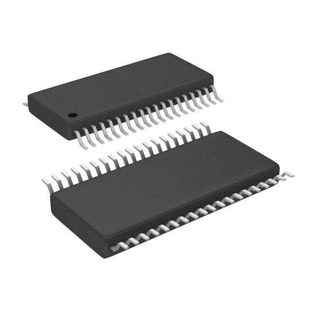
| 描述 | IC A/D CONV 16BIT SAMPLNG 28SOIC |
| 产品分类 | |
| 品牌 | Linear Technology |
| 数据手册 | http://www.linear.com/docs/1670 |
| 产品图片 |
|
| 产品型号 | LTC1605CSW#PBF |
| rohs | 无铅 / 符合限制有害物质指令(RoHS)规范要求 |
| 产品系列 | - |
| 产品目录页面 | |
| 位数 | 16 |
| 供应商器件封装 | 28-SOIC |
| 其它名称 | LTC1605CSWPBF |
| 包装 | 管件 |
| 安装类型 | 表面贴装 |
| 封装/外壳 | 28-SOIC(0.295",7.50mm 宽) |
| 工作温度 | 0°C ~ 70°C |
| 数据接口 | 并联 |
| 标准包装 | 27 |
| 特性 | - |
| 电压源 | 模拟和数字 |
| 转换器数 | 1 |
| 输入数和类型 | 1 个单端,双极 |
| 配用 | /product-detail/zh/DC1255A-A/DC1255A-A-ND/3029458 |
| 采样率(每秒) | 100k |


- 商务部:美国ITC正式对集成电路等产品启动337调查
- 曝三星4nm工艺存在良率问题 高通将骁龙8 Gen1或转产台积电
- 太阳诱电将投资9.5亿元在常州建新厂生产MLCC 预计2023年完工
- 英特尔发布欧洲新工厂建设计划 深化IDM 2.0 战略
- 台积电先进制程称霸业界 有大客户加持明年业绩稳了
- 达到5530亿美元!SIA预计今年全球半导体销售额将创下新高
- 英特尔拟将自动驾驶子公司Mobileye上市 估值或超500亿美元
- 三星加码芯片和SET,合并消费电子和移动部门,撤换高东真等 CEO
- 三星电子宣布重大人事变动 还合并消费电子和移动部门
- 海关总署:前11个月进口集成电路产品价值2.52万亿元 增长14.8%


PDF Datasheet 数据手册内容提取
LTC1605 16-Bit, 100ksps, Sampling ADC FEATURES DESCRIPTION n Single 5V Supply The LTC®1605 is a 100ksps, sampling 16-bit A/D converter n Bipolar Input Range: ±10V that draws only 55mW (typical) from a single 5V supply. n Power Dissipation: 55mW Typ This easy-to-use device includes sample-and-hold, preci- n Guaranteed No Missing Codes sion reference, switched capacitor successive approxima- n Sample Rate: 100ksps tion A/D and trimmed internal clock. n Integral Nonlinearity: ±2.0LSB Max The LTC1605’s input range is an industry standard ±10V. n Signal-to-Noise Ratio: 86dB Typ Maximum DC specs include ±2.0LSB INL and 16-bits no n Operates with Internal or External Reference missing codes over temperature. An external reference can n Internal Synchronized Clock be used if greater accuracy over temperature is needed. n Improved 2nd Source to ADS7805 and AD976 n 28-Lead SSOP and SW Packages The ADC has a microprocessor compatible, 16-bit or two- byte parallel output port. A convert start input and a data APPLICATIONS ready signal (BUSY) ease connections to FIFOs, DSPs and microprocessors. n Industrial Process Control L, LT, LTC, LTM, Linear Technology and the Linear logo are registered trademarks of Linear Technology Corporation. All other trademarks are the property of their respective owners. n Multiplexed Data Acquisition Systems n High Speed Data Acquisition for PCs n Digital Signal Processing TYPICAL APPLICATION Low Power, 100kHz, 16-Bit Sampling ADC on 5V Supply Typical INL Curve 5V 2.0 10μF 0.1μF 1.5 28 27 VDIG VANA 1.0 INP1U0VT 200Ω 1 VIN 2200kk SAM1P6L-IBNIGT ADC D15 TO D0 165 T TOO 1 232 1OP6AR-R B2AI TBLYLETLE L (LSBs) 0.50 N BUS I–0.5 33.2k 4k 10k –1.0 4 CAP BUSY 26 –1.5 2.2μF BUFFER CS 25 –2.0 CONTROL DIGITAL 0 16384 32768 49152 65535 LOGIC AND CONTROL 3 REF 4k REFERENCE TIMING R/C 24 SIGNALS CODE BYTE 23 1605 (cid:127) TA02 2.2μF AGND1 AGND2 DGND 2 5 14 1605 (cid:127) TA01 1605fd 1 For more information www.linear.com/LTC1605
LTC1605 ABSOLUTE MAXIMUM RATINGS PIN CONFIGURATION (Notes 1, 2) V ..........................................................................7V TOP VIEW ANA VDIG to VANA ............................................................0.3V VIN 1 28 VDIG VDIG ...........................................................................7V AGND1 2 27 VANA Ground Voltage Difference REF 3 26 BUSY DGND, AGND1 and AGND2 ................................±0.3V CAP 4 25 CS AGND2 5 24 R/C Analog Inputs (Note 3) D15 (MSB) 6 23 BYTE V .....................................................................±25V IN D14 7 22 D0 CAP .............................V + 0.3V to AGND2 – 0.3V ANA D13 8 21 D1 REF ....................................Indefinite Short to AGND2 D12 9 20 D2 ..........................................Momentary Short to V ANA D11 10 19 D3 Digital Input Voltage (Note 4) ..........DGND – 0.3V to 10V D10 11 18 D4 Digital Output Voltage ........VDGND – 0.3V to VDIG + 0.3V D9 12 17 D5 Power Dissipation ..............................................500mW D8 13 16 D6 Operating Ambient Temperature Range DGND 14 15 D7 LTC1605C ................................................0°C to 70°C OBSOLETE PACKAGE G PACKAGE SW PACKAGE LTC1605I .............................................–40°C to 85°C N PACKAGE 28-LEAD PLASTIC SSOP 28-LEAD PLASTIC SO WIDE 28-LEAD PDIP Storage Temperature Range ..................–65°C to 150°C TJMAX = 125°C, θJA = 95°C/W (G) Lead Temperature (Soldering, 10 sec) ...................300°C TJMAX = 125°C, θJA = 130°C/W (N) TJMAX = 125°C, θJA = 130°C/W (SW) EXPOSED PAD (PIN #) IS GND, MUST BE SOLDERED TO PCB ORDER INFORMATION LEAD FREE FINISH TAPE AND REEL PART MARKING PACKAGE DESCRIPTION TEMPERATURE RANGE LTC1605ACG#PBF LTC1605ACG#TRPBF 1605ACG 28-Lead Plastic SSOP 0°C to 70°C LTC1605AIG#PBF LTC1605AIG#TRPBF 1605AIG 28-Lead Plastic SSOP –40°C to 85°C LTC1605CG#PBF LTC1605CG#TRPBF 1605CG 28-Lead Plastic SSOP 0°C to 70°C LTC1605IG#PBF LTC1605IG#TRPBF 1605IG 28-Lead Plastic SSOP –40°C to 85°C LTC1605ACSW#PBF LTC1605ACSW#TRPBF 1605ACSW 28-Lead Plastic SO Wide 0°C to 70°C LTC1605AISW#PBF LTC1605AISW#TRPBF 1605AISW 28-Lead Plastic SO Wide –40°C to 85°C LTC1605CSW#PBF LTC1605CSW#TRPBF 1605CSW 28-Lead Plastic SO Wide 0°C to 70°C LTC1605ISW#PBF LTC1605ISW#TRPBF 1605ISW 28-Lead Plastic SO Wide –40°C to 85°C OBSOLETE PACKAGE LTC1605CN#PBF LTC1605CN#TRPBF 1605CN 28-Lead PDIP 0°C to 70°C LTC1605IN#PBF LTC1605IN#TRPBF 1605IN 28-Lead PDIP –40°C to 85°C Consult LTC Marketing for parts specified with wider operating temperature ranges. Consult LTC Marketing for information on nonstandard lead based finish parts. For more information on lead free part marking, go to: http://www.linear.com/leadfree/ For more information on tape and reel specifications, go to: http://www.linear.com/tapeandreel/ 1605fd 2 For more information www.linear.com/LTC1605
LTC1605 CONVERTER CHARACTERISTICS The l denotes the specifications which apply over the full operating temperature range, otherwise specifications are at T = 25°C. (Notes 5, 6) A LTC1605 LTC1605A PARAMETER CONDITIONS MIN TYP MAX MIN TYP MAX UNITS Resolution l 16 16 Bits No Missing Codes l 15 16 Bits Transition Noise 1.0 1.0 LSB Integral Linearity Error (Note 7) l ±3 ±2 LSB Bipolar Zero Error Ext. Reference = 2.5V (Note 8) l ±10 ±10 mV Bipolar Zero Error Drift ±2 ±2 ppm/°C Full-Scale Error Drift ±7 ±5 ppm/°C Full-Scale Error Ext. Reference = 2.5V (Notes 12, 13) l ±0.50 ±0.25 % Full-Scale Error Drift Ext. Reference = 2.5V ±2 ±2 ppm/°C Power Supply Sensitivity V = 5V ±5% (Note 9) ±8 ±8 LSB DD V = V = V ANA DIG DD ANALOG INPUT The l denotes the specifications which apply over the full operating temperature range, otherwise specifications are at T = 25°C. (Note 5) A CONDITIONS LTC1605/LTC1605A SYMBOL PARAMETER MIN TYP MAX UNITS V Analog Input Range (Note 9) 4.75V ≤ V ≤ 5.25V, 4.75V ≤ V ≤ 5.25V l ±10 V IN ANA DIG C Analog Input Capacitance 10 pF IN R Analog Input Impedance 20 kΩ IN DYNAMIC ACCURACY (Notes 5, 14) LTC1605/LTC1605A SYMBOL PARAMETER CONDITIONS MIN TYP MAX UNITS S/(N + D) Signal-to-(Noise + Distortion) Ratio 1kHz Input Signal (Note 14) 87.5 dB 10kHz Input Signal 87 dB 20kHz, –60dB Input Signal 30 dB THD Total Harmonic Distortion 1kHz Input Signal, First 5 Harmonics –102 dB 10kHz Input Signal, First 5 Harmonics –94 dB Peak Harmonic or Spurious Noise 1kHz Input Signal –102 dB 10kHz Input Signal –94 dB Full-Power Bandwidth (Note 15) 275 kHz Aperture Delay 40 ns Aperture Jitter Sufficient to Meet AC Specs Transient Response Full-Scale Step (Note 9) 2 µs Overvoltage Recovery (Note 16) 150 ns 1605fd 3 For more information www.linear.com/LTC1605
LTC1605 INTERNAL REFERENCE CHARACTERISTICS The l denotes the specifications which apply over the full operating temperature range, otherwise specifications are at T = 25°C. (Note 5) A LTC1605/LTC1605A PARAMETER CONDITIONS MIN TYP MAX UNITS V Output Voltage I = 0 l 2.470 2.500 2.520 V REF OUT V Output Tempco I = 0 ±5 ppm/°C REF OUT Internal Reference Source Current 1 µA External Reference Voltage for Specified Linearity (Notes 9, 10) 2.30 2.50 2.70 V External Reference Current Drain Ext. Reference = 2.5V (Note 9) l 100 µA CAP Output Voltage I = 0 2.50 V OUT DIGITAL INPUTS AND OUTPUTS The l denotes the specifications which apply over the full operating temperature range, otherwise specifications are at T = 25°C. (Note 5) A LTC1605/LTC1605A SYMBOL PARAMETER CONDITIONS MIN TYP MAX UNITS V High Level Input Voltage V = 5.25V l 2.4 V IH DD V Low Level Input Voltage V = 4.75V l 0.8 V IL DD I Digital Input Current V = 0V to V l ±10 µA IN IN DD C Digital Input Capacitance 5 pF IN V High Level Output Voltage V = 4.75V I = –10µA 4.5 V OH DD O I = –200µA l 4.0 V O V Low Level Output Voltage V = 4.75V I = 160µA 0.05 V OL DD O I = 1.6mA l 0.10 0.4 V O I Hi-Z Output Leakage D15 to D0 V = 0V to V , CS High l ±10 µA OZ OUT DD C Hi-Z Output Capacitance D15 to D0 CS High (Note 9) l 15 pF OZ I Output Source Current V = 0V –10 mA SOURCE OUT I Output Sink Current V = V 10 mA SINK OUT DD 1605fd 4 For more information www.linear.com/LTC1605
LTC1605 TIMING CHARACTERISTICS The l denotes the specifications which apply over the full operating temperature range, otherwise specifications are at T = 25°C. (Note 5) A LTC1605/LTC1605A SYMBOL PARAMETER CONDITIONS MIN TYP MAX UNITS f Maximum Sampling Frequency l 100 kHz SAMPLE(MAX) t Conversion Time l 8 µs CONV t Acquisition Time l 2 µs ACQ t Convert Pulse Width (Note 11) l 40 ns 1 t Data Valid Delay After R/C↓ (Note 9) l 8 µs 2 t BUSY Delay from R/C↓ C = 50pF l 65 ns 3 L t BUSY Low 8 µs 4 t BUSY Delay After End of Conversion 220 ns 5 t Aperture Delay 40 ns 6 t Bus Relinquish Time l 10 35 83 ns 7 t BUSY Delay After Data Valid l 50 200 ns 8 t Previous Data Valid After R/C↓ 7.4 µs 9 t R/C to CS Setup Time (Notes 9, 10) 10 ns 10 t Time Between Conversions 10 µs 11 t Bus Access and Byte Delay (Notes 9, 10) 10 83 ns 12 POWER REQUIREMENTS The l denotes the specifications which apply over the full operating temperature range, otherwise specifications are at T = 25°C. (Note 5) A LTC1605/LTC1605A SYMBOL PARAMETER CONDITIONS MIN TYP MAX UNITS V Positive Supply Voltage (Notes 9, 10) 4.75 5.25 V DD I Positive Supply Current l 11 16 mA DD P Power Dissipation 55 80 mW DIS Note 1: Stresses beyond those listed under Absolute Maximum Ratings Note 8: Bipolar offset is the offset voltage measured from –0.5LSB when the may cause permanent damage to the device. Exposure to any Absolute output code flickers between 0000 0000 0000 0000 and 1111 1111 1111 1111. Maximum Rating condition for extended periods may affect device Note 9: Guaranteed by design, not subject to test. reliability and lifetime. Note 10: Recommended operating conditions. Note 2: All voltage values are with respect to ground with DGND, AGND1 Note 11: With CS low the falling R/C edge starts a conversion. If R/C and AGND2 wired together (unless otherwise noted). returns high at a critical point during the conversion it can create small Note 3: When these pin voltages are taken below ground or above VANA errors. For best results ensure that R/C returns high within 3µs after the = VDIG = VDD, they will be clamped by internal diodes. This product can start of the conversion. handle input currents of greater than 100mA below ground or above V DD Note 12: As measured with fixed resistors shown in Figure 4. Adjustable to without latch-up. zero with external potentiometer. Note 4: When these pin voltages are taken below ground, they will be Note 13: Full-scale error is the worst-case of –FS or +FS untrimmed clamped by internal diodes. This product can handle input currents of deviation from ideal first and last code transitions, divided by the transition 90mA below ground without latchup. These pins are not clamped to V . DD voltage (not divided by the full-scale range) and includes the effect of Note 5: VDD = 5V, fSAMPLE = 100kHz, tr = tf = 5ns unless otherwise specified. offset error. Note 6: Linearity, offset and full-scale specifications apply for a VIN input Note 14: All specifications in dB are referred to a full-scale ±10V input. with respect to ground. Note 15: Full-power bandwidth is defined as full-scale input frequency at which Note 7: Integral nonlinearity is defined as the deviation of a code from a a signal-to-(noise + distortion) degrades to 60dB or 10 bits of accuracy. straight line passing through the actual end points of the transfer curve. Note 16: Recovers to specified performance after (2 • FS) input The deviation is measured from the center of the quantization band. overvoltage. 1605fd 5 For more information www.linear.com/LTC1605
LTC1605 TYPICAL PERFORMANCE CHARACTERISTICS Change in CAP Voltage Supply Current vs Supply Voltage Supply Current vs Temperature vs Load Current 12.5 12.0 0.05 fSAMPLE = 100kHz fSAMPLE = 100kHz 0.04 12.0 A) 0.03 m V) 0.02 mA) NT (11.5 GE ( 0.01 PPLY CURRENT (111011...505 E SUPPLY CURRE11.0 GE IN CAP VOLTA–––––00000.....00000012345 SU10.0 OSITIV10.5 CHAN––00..0067 P –0.08 –0.09 9.5 10.0 –0.10 4.50 4.75 5.00 5.25 5.50 –50 –25 0 25 50 75 100 –80 –70 –60 –50 –40 –30 –20 –10 0 10 TEMPERATURE (°C) LOAD CURRENT (mA) SUPPLY VOLTAGE (V) 1605 (cid:127) TPC01 1605 (cid:127) TPC02 1605 (cid:127) TPC03 Power Supply Feedthrough vs Typical INL Curve Typical DNL Curve Ripple Frequency 2.0 2.0 –20 1.5 1.5 B) d H (–30 1.0 1.0 G U O INL (LSBs)–00..505 DNL (LSBs)–00..505 PLY FEEDTHR––5400 P U S –1.0 –1.0 R WE–60 –1.5 –1.5 O P –2.0 –2.0 –70 0 16384 32768 49152 65535 0 16384 32768 49152 65535 1 10 100 1k 10k 100k 1M CODE CODE RIPPLE FREQUENCY (Hz) 1605 (cid:127) TPC04 1605 (cid:127) TPC05 1605 (cid:127) TPC06 LTC1605 Nonaveraged 4096 Point FFT Plot 0 –10 –20 fSAMPLE = 100kHz fIN = 1kHz –30 SINAD = 87.5dB B) –40 THD = –101.7dB E (d –50 D –60 U NIT –70 AG –80 M –90 –100 –110 –120 –130 0 5 10 15 20 25 30 35 40 45 50 FREQUENCY (kHz) 1605 (cid:127) TPC07 1605fd 6 For more information www.linear.com/LTC1605
LTC1605 TYPICAL PERFORMANCE CHARACTERISTICS Total Harmonic Distortion vs SINAD vs Input Frequency Input Frequency 90 –70 89 B) d 88 ON ( –80 TI 87 R O NAD (dB) 8865 NIC DIST –90 SI MO 84 R A 83 L H–100 A T O 82 T 81 –110 1 10 100 1 10 100 INPUT FREQUENCY (kHz) INPUT FREQUENCY (kHz) 1605 (cid:127) TPC08 1605 (cid:127) TPC09 PIN FUNCTIONS VIN (Pin 1): Analog Input. Connect through a 200Ω resis- R/C (Pin 24): Read/Convert Input. With CS low, a falling tor to the analog input. Full-scale input range is ±10V. edge on R/C puts the internal sample-and-hold into the hold state and starts a conversion. With CS low, a rising AGND1 (Pin 2): Analog Ground. Tie to analog ground plane. edge on R/C enables the output data bits. REF (Pin 3): 2.5V Reference Output. Bypass with 2.2µF tan- CS (Pin 25): ChipSelect. Internally OR’d with R/C. With R/C talum capacitor. Can be driven with an external reference. low, a falling edge on CS will initiate a conversion. With CAP (Pin 4): Reference Buffer Output. Bypass with 2.2µF R/C high, a falling edge on CS will enable the output data. tantalum capacitor. BUSY (Pin 26): Output Shows Converter Status. It is low AGND2 (Pin 5): Analog Ground. Tie to analog ground plane. when a conversion is in progress. Data valid on the rising D15 to D8 (Pins 6 to 13): Three-State Data Outputs. Hi-Z edge of BUSY. CS or R/C must be high when BUSY rises state when CS is high or when R/C is low. or another conversion will start without time for signal acquisition. DGND (Pin 14): Digital Ground. V (Pin 27): 5V Analog Supply. Bypass to ground with ANA D7 to D0 (Pins 15 to 22): Three-State Data Outputs. Hi-Z a 0.1µF ceramic and a 10µF tantalum capacitor. state when CS is high or when R/C is low. V (Pin 28): 5V Digital Supply. Connect directly to Pin 27. DIG BYTE (Pin 23): Byte Select. With BYTE low, data will be output with Pin 6 (D15) being the MSB and Pin 22 (D0) being the LSB. With BYTE high the upper eight bits and the lower eight bits will be switched. The MSB is output on Pin 15 and bit 8 is output on Pin 22. Bit 7 is output on Pin 6 and the LSB is output on Pin 13. 1605fd 7 For more information www.linear.com/LTC1605
LTC1605 TEST CIRCUIT Load Circuit for Access Timing Load Circuit for Output Float Delay 5V 5V 1k 1k DBN DBN DBN DBN 1k CL CL 1k 50pF 50pF LTC1605 (cid:127) TC01 LTC1605 (cid:127) TC02 A. HI-Z TO VOH AND VOL TO VOH B. HI-Z TO VOL AND VOH TO VOL A. VOH TO HI-Z B. VOL TO HI-Z FUNCTIONAL BLOCK DIAGRAM CSAMPLE 20k VIN 10k 4k VANA CSAMPLE VDIG ZEROING SWITCHES 4k REF 2.5V REF + REF BUF 16-BIT CAPACITIVE DAC COMP – CAP (2.5V) 16 D15 SUCCESSIVE APPROXIMATION (cid:127) OUTPUT LATCHES (cid:127) AGND1 REGISTER (cid:127) D0 AGND2 INTERNAL DGND CLOCK CONTROL LOGIC LTC1605 (cid:127) BD CS R/C BYTE BUSY 1605fd 8 For more information www.linear.com/LTC1605
LTC1605 APPLICATIONS INFORMATION Conversion Details the end of a conversion, the DAC output balances the V IN input charge. The SAR contents (a 16-bit data word) that The LTC1605 uses a successive approximation algo- represents the V are loaded into the 16-bit output latches. rithm and an internal sample-and-hold circuit to convert IN an analog signal to a 16-bit or two byte parallel output. Driving the Analog Inputs The ADC is complete with a precision reference and an internal clock. The control logic provides easy interface The nominal input range for the LTC1605 is ±10V to microprocessors and DSPs. (Please refer to the Digital or (±4 • VREF) and the input is overvoltage protected to Interface section for the data format.) ±25V. The input impedance is typically 20kΩ, therefore, it should be driven with a low impedance source. Wideband Conversion start is controlled by the CS and R/C inputs. noise coupling into the input can be minimized by placing At the start of conversion the successive approximation a 1000pF capacitor at the input as shown in Figure 2. An register (SAR) is reset. Once a conversion cycle has begun NPO-type capacitor gives the lowest distortion. Place the it cannot be restarted. capacitor as close to the device input pin as possible. If During the conversion, the internal 16-bit capacitive DAC an amplifier is to be used to drive the input, care should output is sequenced by the SAR from the most significant be taken to select an amplifier with adequate accuracy, bit (MSB) to the least significant bit (LSB). Referring to linearity and noise for the application. The following list Figure 1, V is connected through the resistor divider to the is a summary of the op amps that are suitable for driving IN sample-and-hold capacitor during the acquire phase and the LTC1605. More detailed information is available at the comparator offset is nulled by the autozero switches. www.linear.com. In this acquire phase, a minimum delay of 2µs will provide 200Ω enough time for the sample-and-hold capacitor to acquire AIN VIN the analog signal. During the convert phase, the autozero 1000pF 33.2k switches open, putting the comparator into the compare CAP mode. The input switch switches C to ground, SAMPLE 1605 (cid:127) F02 injecting the analog input charge onto the summing junc- Figure 2. Analog Input Filtering tion. This input charge is successively compared with the LT®1007: Low noise precision amplifier. 2.7mA supply binary-weighted charges supplied by the capacitive DAC. current ±5V to ±15V supplies. Gain bandwidth product Bit decisions are made by the high speed comparator. At 8MHz. DC applications. SAMPLE LT1097: Low cost, low power precision amplifier. 300µA supply current. ±5V to ±15V supplies. Gain bandwidth RIN1 SAMPLE CSAMPLE SI product 0.7MHz. DC applications. VIN – HOLD LT1227: 140MHz video current feedback amplifier. 10mA RIN2 + supply current. ±5V to ±15V supplies. Low noise and low CDAC COMPARATOR distortion. DAC VDAC S LT1360: 37MHz voltage feedback amplifier. 3.8mA supply A R current. ±5V to ±15V supplies. Good AC/DC specs. LT1363: 50MHz voltage feedback amplifier. 6.3mA supply 16-BIT LATCH current. Good AC/DC specs. 1605 (cid:127) F01 Figure 1. LTC1605 Simplified Equivalent Circuit LT1364/LT1365: Dual and quad 50MHz voltage feedback amplifiers. 6.3mA supply current per amplifier. Good AC/ DC specs. 1605fd 9 For more information www.linear.com/LTC1605
LTC1605 APPLICATIONS INFORMATION Internal Voltage Reference is adjusted until the output code is changing between 0111 1111 1111 1110 and 0111 1111 1111 1111. Figure 6 shows The LTC1605 has an on-chip, temperature compensated, the bipolar transfer characteristic of the LTC1605. curvature corrected, bandgap reference, which is factory trimmed to 2.50V. The full-scale range of the ADC is 1 equal to (±4 • V ) or nominally ±10V. The output of the 10V INPUT VIN REF 200Ω 2 AGND1 reference is connected to the input of a unity-gain buffer 1% 2.2μF through a 4k resistor (see Figure 3). The input to the buffer 33.2k + 3 LTC1605 1% REF or the output of the reference is available at REF (Pin 3). 4 CAP + The internal reference can be overdriven with an external 2.2μF 5 reference if more accuracy is needed. The buffer output AGND2 drives the internal DAC and is available at CAP (Pin 4). The 1605 (cid:127) F04 CAP pin can be used to drive a steady DC load of less than Figure 4. ±10V Input Without Trim 2mA. Driving an AC load is not recommended because it 1 can cause the performance of the converter to degrade. 10V INPUT VIN 200Ω 2 AGND1 1% 2.2μF REF 3 4k BANDGAP + (2.5V) REFERENCE 331.2%k 5V 3 REF 2.2μF + VANA 576k LTC1605 R4 50k 4 + CAP – R3 2.2μF 50k 5 CAP 4 AGND2 (2.5V) 1605 (cid:127) F05 INTERNAL 2.2μF CAPACITOR Figure 5. ±10V Input with Offset and Gain Trim DAC 1605 (cid:127) F03 011...111 011...110 BIPOLAR ZERO Figure 3. Internal or External Reference Source E 000...001 For minimum code transition noise the REF pin and the OD C 000...000 CAP pin should each be decoupled with a capacitor to UT P 111...111 T filter wideband noise from the reference and the buffer OU 111...110 (2.2µF tantalum). 100...001 FS = 20V Offset and Gain Adjustments 100...000 1LSB = FS/65536 The LTC1605 offset and full-scale errors have been trimmed –FS/2 –1 0V 1 FS/2 – 1LSB LSB LSB at the factory with the external resistors shown in Figure 4. INPUT VOLTAGE (V) 1605 (cid:127) F06 This allows for external adjustment of offset and full scale in Figure 6. LTC1605 Bipolar Transfer Characteristics applications where absolute accuracy is important. See Figure DC Performance 5 for the offset and gain trim circuit. First adjust the offset to zero by adjusting resistor R3. Apply an input voltage of One way of measuring the transition noise associated –152.6mV (–0.5LSB) and adjust R3 so the code is changing with a high resolution ADC is to use a technique where between 1111 1111 1111 1111 and 0000 0000 0000 0000. a DC signal is applied to the input of the ADC and the The gain error is trimmed by adjusting resistor R4. An input resulting output codes are collected over a large number voltage of 9.999542V (+FS – 1.5LSB) is applied to V and R4 of conversions. For example in Figure 7 the distribution of IN 1605fd 10 For more information www.linear.com/LTC1605
LTC1605 TYPICAL APPLICATIONS output code is shown for a DC input that has been digitized Timing and Control 10000 times. The distribution is Gaussian and the RMS Conversion start and data read are controlled by two code transition is about 1LSB. digital inputs: CS and R/C. To start a conversion and put 4500 the sample-and-hold into the hold mode bring CS and 4000 R/C low for no less than 40ns. Once initiated it cannot be 3500 restarted until the conversion is complete. Converter status is indicated by the BUSY output and this is low while the 3000 conversion is in progress. T2500 N U CO2000 There are two modes of operation. The first mode is shown 1500 in Figure 8. The digital input R/C is used to control the 1000 start of conversion. CS is tied low. When R/C goes low 500 the sample-and-hold goes into the hold mode and a con- 0 version is started. BUSY goes low and stays low during –5 –4 –3 –2 –1 0 1 2 3 4 5 the conversion and will go back high after the conversion CODE has been completed and the internal output shift registers 1605 (cid:127) F07 Figure 7. Histogram for 10000 Conversions have been updated. R/C should remain low for no less than 40ns. During the time R/C is low the digital outputs are in DIGITAL INTERFACE a Hi-Z state. R/C should be brought back high within 3µs after the start of the conversion to ensure that no errors Internal Clock occur in the digitized result. The second mode, shown in The ADC has an internal clock that is trimmed to achieve Figure 9, uses the CS signal to control the start of a con- a typical conversion time of 7µs. No external adjustments version and the reading of the digital output. In this mode are required and, with the typical acquisition time of 1µs, the R/C input signal should be brought low no less than throughput performance of 100ksps is assured. 10ns before the falling edge of CS. The minimum pulse width for CS is 40ns. When CS falls, BUSY goes low and will stay low until the end of the conversion. BUSY will go high after the conversion has been completed. The new data is valid when CS is brought back low again to initiate t1 R/C t11 t2 BUSY t3 t4 t6 t5 MODE ACQUIRE CONVERT ACQUIRE CONVERT tCONV tACQ t9 PREVIOUS PREVIOUS DATA DATA DATA MODE DATA VALID HI-Z DATA VALID NOT VALID VALID HI-Z VALID t7 t8 1605 (cid:127) F08 Figure 8. Conversion Timing with Outputs Enabled After Conversion (CS Tied Low) 1605fd 11 For more information www.linear.com/LTC1605
LTC1605 APPLICATIONS INFORMATION t10 t10 t10 t10 R/C t1 t1 CS t3 t4 BUSY t6 MODE ACQUIRE CONVERT ACQUIRE tCONV DATA BUS HI-Z DATA HI-Z VALID t12 t7 1605 (cid:127) F09 Figure 9. Using CS to Control Conversion and Read Timing t10 t10 R/C CS BYTE HI-Z HI-Z PINS 6 TO 13 HIGH BYTE LOW BYTE t12 t12 t7 HI-Z HI-Z PINS 15 TO 22 LOW BYTE HIGH BYTE 1605 (cid:127) F10 Figure 10. Using CS and BYTE to Control Data Bus Read Timing 0 –10 –20 fSAMPLE = 100kHz –30 fIN = 1kHz SINAD = 87.5dB B) –40 THD = –101.7dB d –50 DE ( –60 U NIT –70 AG –80 M –90 –100 –110 –120 –130 0 5 10 15 20 25 30 35 40 45 50 FREQUENCY (kHz) 1605 (cid:127) F11 Figure 11. LTC1605 Nonaveraged 4096 Point FFT Plot 1605fd 12 For more information www.linear.com/LTC1605
LTC1605 APPLICATIONS INFORMATION a read. Again it is recommended that both R/C and CS band between DC and half the sampling frequency. THD return high within 3µs after the start of the conversion. is expressed as: Output Data V22+V32+V42+...V 2 THD=20Log N The output data can be read as a 16-bit word or it can be V1 read as two 8-bit bytes. The format of the output data is where V1 is the RMS amplitude of the fundamental two’s complement. The digital input pin BYTE is used to frequency and V2 through V are the amplitudes of the control the two byte read. With the BYTE pin low the first N second through Nth harmonics. eight MSBs are output on the D15 to D8 pins and the eight LSBs are output on the D7 to D0 pins. When the Board Layout, Power Supplies and Decoupling BYTE pin is taken high the eight LSBs replace the eight MSBs (Figure 10). Wire wrap boards are not recommended for high reso- lution or high speed A/D converters. To obtain the best Dynamic Performance performance from the LTC1605, a printed circuit board is required. Layout for the printed circuit board should FFT (Fast Fourier Transform) test techniques are used to ensure the digital and analog signal lines are separated test the ADC’s frequency response, distortion and noise as much as possible. In particular, care should be taken at the rated throughput. By applying a low distortion sine not to run any digital track alongside an analog signal wave and analyzing the digital output using an FFT algo- track or underneath the ADC. The analog input should be rithm, the ADC’s spectral content can be examined for screened by AGND. frequencies outside the fundamental. Figure 11 shows a typical LTC1605 FFT plot which yields a SINAD of 87.5dB Figures 12 through 15 show a layout for a suggested evalu- and THD of –102dB. ation circuit which will help obtain the best performance from the 16-bit ADC. Pay particular attention to the design Signal-to-Noise Ratio of the analog and digital ground planes. The DGND pin of the LTC1605 can be tied to the analog ground plane. The Signal-to-Noise and Distortion Ratio (SINAD) is the Placing the bypass capacitor as close as possible to the ratio between the RMS amplitude of the fundamental input power supply, the reference and reference buffer output is frequency to the RMS amplitude of all other frequency very important. Low impedance common returns for these components at the A/D output. The output is band limited bypass capacitors are essential to low noise operation of to frequencies from above DC and below half the sampling the ADC, and the foil width for these tracks should be as frequency. Figure 11 shows a typical SINAD of 87.5dB with wide as possible. Also, since any potential difference in a 100kHz sampling rate and a 1kHz input. grounds between the signal source and ADC appears as Total Harmonic Distortion an error voltage in series with the input signal, attention should be paid to reducing the ground circuit impedance Total Harmonic Distortion (THD) is the ratio of the RMS as much as possible. The digital output latches and the sum of all harmonics of the input signal to the fundamental onboard sampling clock have been placed on the digital itself. The out-of-band harmonics alias into the frequency ground plane. The two ground planes are tied together at the power supply ground connection. 1605fd 13 For more information www.linear.com/LTC1605
LTC1605 TYPICAL APPLICATIONS Figure 12. Component Side Silkscreen for the Suggested LTC1605 Evaluation Circuit ANALOG DIGITAL ANALOG GROUND PLANE GROUND PLANE GROUND PLANE Figure 13. Bottom Side Showing Analog Ground Plane Figure 14. Component Side Showing Separate Analog and Digital Ground Plane 1605fd 14 For more information www.linear.com/LTC1605
LTC1605 JP2LEDENABLE 1605_07d.eps D15 D14 D13 D12 D11 D10 D9 D8 D7 D6 D5 D4 D3 D2 D1 D0 D15 CLK GND GND D15 D14 D13 D12 D11 D10 D9 D8 D7 D6 D5 D4 D3 D2 D1 D0 1 2 3 4 5 6 7 8 9 10 11 12 13 14 15 16 17 18 19 20 R15, 1.2k R14, 1.2k R13, 1.2k R12, 1.2k R11, 1.2k R10, 1.2k R9, 1.2k R8, 1.2k R7, 1.2k R6, 1.2k R5, 1.2k R4, 1.2k R3, 1.2k R2, 1.2k R1, 1.2k R0, 1.2k 2 1U4AHC04 19 18 17 16 15 14 13 12 74 19 18 17 16 15 14 13 12 C14C150.1μF10μF U274HC5742D15D0Q03D14Q1D14D13Q2D25D12Q3D36D11Q4D47D10Q5D58D9Q6D69 D8Q7D71 OC11 CLK U374HC5742D0Q0D03D1Q1D14D2Q2D25D3Q3D36D4Q4D47D5Q5D58D6Q6D69 D7Q7D71 OC11 CLK U4C74HC0465 C115pF hematic c S C130.1μF R201K Circuit VCC C11C120.1μF0.1μF U1LTC1605 6D15D15VIN 7D14AGND1D14 8D13REFD13 9D12CAPD12 10D11AGND2D11 11D10DGNDD10 12D9BYTED9 13D8R/CD8 15D7CSD7 16D6BUSYD6 17D5VD5ANA 18D4VD4DIG 19D3D3 20D2D2 21D1D1 D022D0 U4B74HC0443 ested Evaluation 1 2 3 4 5 14 23 24 25 26 27 28 gg DIGITAL I.C. BYPASSINGVDD C9C100.1μF0.1μF R182001% C16R191000pF33.2kJP11% C3EXTINTVREF0.1μFC2C42.2μF2.2μFC5C170.1μF10μF VCC 3REVERSEJP42BYTE 1NORNALVKK C710μF U6A74HC221C814AQ0.1μF213BQ3CLK CEXT15RCEXTR21, 2k VCC 3VJP5CC2CS 1GND Figure 15. LTC1605 Su VCCR1620 C622μF10V JP32 VCC VKKVIN7V TO 15V13E1VVININU5+LT1121D16MBR0520GND2GNDE2 AIN1J2VKK218NC1NC227INPUTHEATER36TEMPOUT45TRIMGND U9LT1019-2.5 U4EU4D74HC0474HC04EXT_CLK1011819J1R17251 VCCU7U83EXT74HC1601MHz, OSCCLK11NACLR91INTLOAD232OUTGNDCLK10ENT715RCOENP611QDD512QCC413QBB314QAA 1605fd 15 For more information www.linear.com/LTC1605
LTC1605 PACKAGE DESCRIPTION Please refer to http://www.linear.com/designtools/packaging/ for the most recent package drawings. G Package 28-Lead Plastic SSOP (5.3mm) (Reference LTC DWG # 05-08-1640) 9.90 – 10.50* (.390 – .413) 1.25 ±0.12 2827262524232221201918171615 7.8 – 8.2 5.3 – 5.7 7.40 – 8.20 (.291 – .323) 0.42 ±0.03 0.65 BSC RECOMMENDED SOLDER PAD LAYOUT 1 2 3 4 5 6 7 8 9 1011121314 5.00 – 5.60** 2.0 (.197 – .221) (.079) MAX 0° – 8° 0.09 – 0.25 0.55 – 0.95 0.65 (.0035 – .010) (.022 – .037) (.0256) BSC 0.05 NOTE: 0.22 – 0.38 (.002) 1. CONTROLLING DIMENSION: MILLIMETERS (.009 – .015) MIN MILLIMETERS TYP G28 SSOP 0204 2. DIMENSIONS ARE IN (INCHES) 3. DRAWING NOT TO SCALE *DIMENSIONS DO NOT INCLUDE MOLD FLASH. MOLD FLASH SHALL NOT EXCEED .152mm (.006") PER SIDE **DIMENSIONS DO NOT INCLUDE INTERLEAD FLASH. INTERLEAD FLASH SHALL NOT EXCEED .254mm (.010") PER SIDE N Package 28-Lead Plastic PDIP (Narrow .300 Inch) (Reference LTC DWG # 05-08-1510 Rev I) 1.400* (35.560) MAX 28 27 26 25 24 23 22 21 20 19 18 17 16 15 .240 – .295* (6.096 – 7.493) 1 2 3 4 5 6 7 8 9 10 11 12 13 14 .130 ±.005 .045 – .065 (3.302 ±0.127) (1.143 – 1.651) .020 (0.508) MIN .065 (1.651) TYP .120 N28 REV I 0711 (3.048) .005 .100 .018 ±.003 MIN (0.127) (2.54) (0.457 ±0.076) MIN BSC NOTE: INCHES 1. DIMENSIONS ARE MILLIMETERS *THESE DIMENSIONS DO NOT INCLUDE MOLD FLASH OR PROTRUSIONS. MOLD FLASH OR PROTRUSIONS SHALL NOT EXCEED .010 INCH (0.254mm) OBSOLETE PACKAGE 1605fd 16 For more information www.linear.com/LTC1605
LTC1605 REVISION HISTORY (Revision history begins at Rev D) REV DATE DESCRIPTION PAGE NUMBER D 07/15 Obsoleted 28-Lead PDIP Package 2, 16 1605fd Information furnished by Linear Technology Corporation is believed to be accurate and reliable. 17 However, no responsibility is assumed for its use. Linear Technology Corporation makes no representa- tion that the interconneFcotior nm oof irtse ciinrcfouirtms aast dioensc wribwedw h.leinreeina rw.cilol nmot/ LinTfCrin1g6e0 o5n existing patent rights.
LTC1605 PACKAGE DESCRIPTION Please refer to http://www.linear.com/designtools/packaging/ for the most recent package drawings. SW Package 28-Lead Plastic Small Outline (Wide .300 Inch) (Reference LTC DWG # 05-08-1620) .030 ±.005 .050 BSC .045 ±.005 TYP .697 – .712 (17.70 – 18.08) N NOTE 4 28 27 26 25 24 23 22 21 20 19 18 17 16 15 N .420 .325 ±.005 MIN NOTE 3 .394 – .419 (10.007 – 10.643) 1 2 3 N/2 N/2 RECOMMENDED SOLDER PAD LAYOUT .291 – .299 1 2 3 4 5 6 7 8 9 10 11 12 13 14 (7.391 – 7.595) NOTE 4 .093 – .104 .037 – .045 .010 – .029 × 45° (2.362 – 2.642) (0.940 – 1.143) (0.254 – 0.737) .005 (0.127) RAD MIN 0° – 8° TYP .050 .009 – .013 (1.270) .004 – .012 (0.229 – 0.330) NOTE 3 BSC (0.102 – 0.305) .014 – .019 .016 – .050 (0.356 – 0.482) (0.406 – 1.270) TYP NOTE: INCHES 1. DIMENSIONS IN (MILLIMETERS) S28 (WIDE) 0502 2. DRAWING NOT TO SCALE 3. PIN 1 IDENT, NOTCH ON TOP AND CAVITIES ON THE BOTTOM OF PACKAGES ARE THE MANUFACTURING OPTIONS. THE PART MAY BE SUPPLIED WITH OR WITHOUT ANY OF THE OPTIONS 4. THESE DIMENSIONS DO NOT INCLUDE MOLD FLASH OR PROTRUSIONS. MOLD FLASH OR PROTRUSIONS SHALL NOT EXCEED .006" (0.15mm) RELATED PARTS PART NUMBER DESCRIPTION COMMENTS LT1019-2.5 Precision Bandgap Reference 0.05% Max, 5ppm/°C Max LTC1274/LTC1277 Low Power 12-Bit, 100ksps ADCs 10mW Power Dissipation, Parallel/Byte Interface LTC1415 Single 5V, 12-Bit, 1.25Msps ADC 55mW Power Dissipation, 72dB SINAD LTC1419 Low Power 14-Bit, 800ksps ADC True 14-Bit Linearity, 81.5dB SINAD, 150mW Dissipation LT1460-2.5 Micropower Precision Series Reference 0.075% Max, 10ppm/°C Max, Only 130µA Supply Current LTC1594/LTC1598 Micropower 4-/8-Channel 12-Bit ADCs Serial I/O, 3V and 5V Versions 1605fd 18 Linear Technology Corporation LT 0715 REV D • PRINTED IN USA 1630 McCarthy Blvd., Milpitas, CA 95035-7417 For more information www.linear.com/LTC1605 (408) 432-1900 ● FAX: (408) 434-0507 ● www.linear.com/LTC1605 LINEAR TECHNOLOGY CORPORATION 2005