ICGOO在线商城 > 集成电路(IC) > 数据采集 - 数模转换器 > LTC1450CG#PBF

 Datasheet下载
- 型号: LTC1450CG#PBF
- 制造商: LINEAR TECHNOLOGY
- 库位|库存: xxxx|xxxx
- 要求:
| 数量阶梯 | 香港交货 | 国内含税 |
| +xxxx | $xxxx | ¥xxxx |
查看当月历史价格
查看今年历史价格
LTC1450CG#PBF产品简介:
ICGOO电子元器件商城为您提供LTC1450CG#PBF由LINEAR TECHNOLOGY设计生产,在icgoo商城现货销售,并且可以通过原厂、代理商等渠道进行代购。 LTC1450CG#PBF价格参考。LINEAR TECHNOLOGYLTC1450CG#PBF封装/规格:数据采集 - 数模转换器, 12 位 数模转换器 1 24-SSOP。您可以下载LTC1450CG#PBF参考资料、Datasheet数据手册功能说明书,资料中有LTC1450CG#PBF 详细功能的应用电路图电压和使用方法及教程。
LTC1450CG#PBF 是由 Linear Technology(现为 Analog Devices 旗下品牌)生产的一款数模转换器(DAC),属于数据采集类器件。该芯片为12位、电压输出型、单通道DAC,采用8引脚PDIP封装,具有较高的精度和稳定性。

主要应用场景包括:

1. 工业控制与自动化系统:用于将数字信号转化为模拟电压,以驱动执行机构如阀门、电机或传感器,实现对温度、压力等物理参数的精确控制。

2. 测试与测量设备:在自动测试设备(ATE)、示波器、信号发生器等仪器中,作为高精度信号生成模块,提供稳定的参考电压。

3. 通信系统:用于调制解调器、无线基站或其他通信设备中的模拟信号合成,支持信号调节与校准功能。

4. 医疗电子设备:如监护仪、诊断设备等,用于生成精准的模拟信号以驱动传感器或显示屏。

5. 音频处理设备:虽然非主流音频DAC,但在某些需要中低速高精度模拟输出的专业音频应用中也可使用。

6. 嵌入式控制系统:在需要精密电压控制的嵌入式系统中,如机器人控制、智能仪表等领域,发挥关键作用。

该DAC具备低功耗、无需外部基准电压等特点,适用于多种中高精度模拟输出需求场景。
| 参数 | 数值 |
| 产品目录 | 集成电路 (IC) |
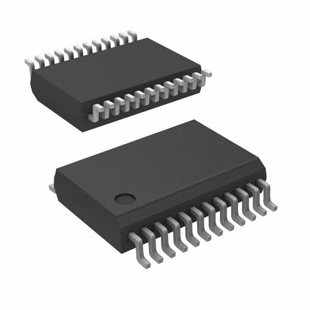
| 描述 | IC D/A CONV 12BIT R-R PAR 24SSOP |
| 产品分类 | |
| 品牌 | Linear Technology |
| 数据手册 | http://www.linear.com/docs/3310 |
| 产品图片 |
|
| 产品型号 | LTC1450CG#PBF |
| rohs | 无铅 / 符合限制有害物质指令(RoHS)规范要求 |
| 产品系列 | - |
| 产品目录页面 | |
| 位数 | 12 |
| 供应商器件封装 | 24-SSOP |
| 其它名称 | LTC1450CGPBF |
| 包装 | 管件 |
| 安装类型 | 表面贴装 |
| 封装/外壳 | 24-SSOP(0.209",5.30mm 宽) |
| 工作温度 | 0°C ~ 70°C |
| 建立时间 | 14µs |
| 数据接口 | 并联 |
| 标准包装 | 59 |
| 电压源 | 单电源 |
| 转换器数 | 1 |
| 输出数和类型 | 1 电压,单极1 电压,双极 |
| 采样率(每秒) | * |


- 商务部:美国ITC正式对集成电路等产品启动337调查
- 曝三星4nm工艺存在良率问题 高通将骁龙8 Gen1或转产台积电
- 太阳诱电将投资9.5亿元在常州建新厂生产MLCC 预计2023年完工
- 英特尔发布欧洲新工厂建设计划 深化IDM 2.0 战略
- 台积电先进制程称霸业界 有大客户加持明年业绩稳了
- 达到5530亿美元!SIA预计今年全球半导体销售额将创下新高
- 英特尔拟将自动驾驶子公司Mobileye上市 估值或超500亿美元
- 三星加码芯片和SET,合并消费电子和移动部门,撤换高东真等 CEO
- 三星电子宣布重大人事变动 还合并消费电子和移动部门
- 海关总署:前11个月进口集成电路产品价值2.52万亿元 增长14.8%


PDF Datasheet 数据手册内容提取
LTC1450/LTC1450L Parallel Input, 12-Bit Rail-to-Rail Micropower DACs in SSOP FEATURES DESCRIPTIOUN n Guaranteed Monotonic The LTC®1450/LTC1450L are complete single supply, rail- n Buffered True Rail-to-Rail Voltage Output to-rail voltage output, 12-bit digital-to-analog converters n 12-Bit Resolution (DACs) in a 24-pin SSOP or PDIP package. They include an n 3V Operation (LTC1450L) ICC: 250m A Typ output buffer amplifier, reference and a double buffered n 5V Operation (LTC1450) ICC: 400m A Typ parallel digital interface. n Parallel 12-Bit or 8 + 4-Bit Double Buffered The LTC1450 operates from a 4.5V to 5.5V supply. The Digital Input output can be pin strapped for 4.095V or 2.048V full-scale. n Internal Reference It has a 2.048V internal reference. n Output Buffer Configurable to Gain of 1 or 2 n Configurable as a Multiplying DAC The LTC1450L operates from a 2.7V to 5.5V supply. The n Internal Power-On Reset output can be pin strapped for 2.5V or 1.22V full-scale. It n Maximum DNL Error: 0.5LSB has a 1.22V internal reference. APPLICATIOUNS The LTC1450/LTC1450L offer true stand-alone perfor- mance. In addition, the reference output, high and low n Digital Calibration reference inputs and gain setting resistor are brought to n Industrial Process Control pins for maximum flexibility. n Automatic Test Equipment , LTC and LT are registered trademarks of Linear Technology Corporation. n Arbitrary Function Generators n Battery-Powered Data Conversion Products n Feedback Control Loops and Gain Control TYPICAL APPLICATIONU LTC1450: 5V(cid:13) LTC1450L: 3V TO 5V D11 (MSB) REFOUT REFHI VCC UPPER(cid:13) REFERENCE(cid:13) 4-BIT(cid:13) LTC1450: 2.048V(cid:13) INPUT(cid:13) LTC1450L: 1.22V Differential Nonlinearity D8 LATCH 12-BIT(cid:13) vs Input Code DAC(cid:13) DATA IN FROM(cid:13) D7 LATCH 0.5(cid:13) MICROPRDOACTEAS SBOURS(cid:13) 1D2-ABCIT(cid:13) + VOUT L0TVC T1O4 540.0: 9(cid:13)5V(cid:13) LOWER(cid:13) LTC1450L: (cid:13) 8-BIT(cid:13) – 0V TO 2.5V INPUT(cid:13) B) LATCH R (LS O 0.0(cid:13) D0 (LSB) RR CSMSB NL E D FROM(cid:13) WR MICROPROCESSOR(cid:13) CSLSB DECODE LOGIC LDAC POWER-ON(cid:13) –0.50 512 1024153620482560307235844095 FROM (cid:13) CLR RESET LLTTCC11445500L(cid:13) CODE SYSTEM RESET GND REFLO X1/X2 1450/50L TA02 1450/50L TA01 1
LTC1450/LTC1450L ABSOLUTE WMAXIWMUWM RATINUGS PACKAGE/ORDER IUNFORWMATIOUN V to GND.............................................. –0.5V to 7.5V CC ORDER PART TOP VIEW Logic Inputs to GND................................ –0.5V to 7.5V NUMBER WR(cid:13) 1(cid:13) 24(cid:13) LDAC(cid:13) V .............................................. –0.5V to V + 0.5V OUT CC CSLSB(cid:13) 2(cid:13) 23(cid:13) CLR(cid:13) REFOUT, REFLO, REFHI, X1/X2..... –0.5V to V + 0.5V LTC1450CG CC CSMSB(cid:13) 3(cid:13) 22(cid:13) X1/X2(cid:13) Maximum Junction Temperature..........................125(cid:176) C (LSB) D0(cid:13) 4(cid:13) 21(cid:13) VOUT(cid:13) LTC1450CN Operating Temperature Range D1(cid:13) 5(cid:13) 20(cid:13) VCC(cid:13) LTC1450IG Commercial...........................................0(cid:176) C to 70(cid:176) C D2(cid:13) 6(cid:13) 19(cid:13) REFOUT(cid:13) LTC1450IN Industrial......................................... –40(cid:176) C to 85(cid:176) C D3(cid:13) 7(cid:13) 18(cid:13) REFHI(cid:13) LTC1450LCG D4(cid:13) 8(cid:13) 17(cid:13) REFLO(cid:13) LTC1450LCN Storage Temperature Range................ –65(cid:176) C to 150(cid:176) C D5(cid:13) 9(cid:13) 16(cid:13) GND(cid:13) LTC1450LIG Lead Temperature (Soldering, 10 sec)................. 300(cid:176) C D6(cid:13) 10(cid:13) 15(cid:13) D11(MSB)(cid:13) LTC1450LIN D7(cid:13) 11(cid:13) 14(cid:13) D10(cid:13) D8 12 13(cid:13) D9 (cid:13) G PACKAGE(cid:13) N PACKAGE(cid:13) 24-LEAD PLASTIC SSOP 24-LEAD PLASTIC PDIP TJMAX = 125(cid:176)C, q JA = 95(cid:176)C/W (G) TJMAX = 125(cid:176)C, q JA = 58(cid:176)C/W (N) Consult factory for Military grade parts. ELECTRICAL CHARACTERISTICS V = 4.5V to 5.5V (LTC1450), 2.7V to 5.5V (LTC1450L), V unloaded, CC OUT REFOUT = REFHI, REFLO = GND = X1/X2, T = T to T , unless otherwise noted. A MIN MAX SYMBOL PARAMETER CONDITIONS MIN TYP MAX UNITS DAC Resolution l 12 Bits DNL Differential Nonlinearity Guaranteed Monotonic (Note 1) l – 0.5 LSB INL Integral Nonlinearity T = 25(cid:176) C – 3.5 LSB A (Note 1) l – 4.0 LSB V Offset Error T = 25(cid:176) C – 12 mV OS A l – 18 mV V TC Offset Error Temperature Coefficient – 15 m V/(cid:176) C OS V Full-Scale Voltage Using Internal Reference, LTC1450, T = 25(cid:176) C 4.065 4.095 4.125 V FS A Using Internal Reference, LTC1450 l 4.045 4.095 4.145 V External 2.048V Reference, LTC1450 l 4.075 4.095 4.115 V Using Internal Reference, LTC1450L, T = 25(cid:176) C 2.470 2.500 2.530 V A Using Internal Reference, LTC1450L l 2.460 2.500 2.540 V External 1.22V Reference, LTC1450L l 2.480 2.500 2.520 V V TC Full-Scale Voltage Temperature Coefficient Using Internal Reference, LTC1450 – 0.10 LSB/(cid:176) C FS Using External Reference, LTC1450/LTC1450L – 0.02 LSB/(cid:176) C Using Internal Reference, LTC1450L – 0.10 LSB/(cid:176) C Reference Output (REFOUT) Reference Output Voltage LTC1450L l 1.195 1.220 1.245 V LTC1450 l 2.008 2.048 2.088 V Reference Output Temperature Coefficient – 0.08 LSB/(cid:176) C Reference Line Regulation l 0.7 – 2 LSB/V Reference Load Regulation 0 £ I £ 100m A, LTC1450L l 0.6 – 3.0 LSB OUT LTC1450 l 0.2 – 1.5 LSB Short-Circuit Current REFOUT Shorted to GND l 80 mA 2
LTC1450/LTC1450L ELECTRICAL CHARACTERISTICS V = 4.5V to 5.5V (LTC1450), 2.7V to 5.5V (LTC1450L), V unloaded, CC OUT REFOUT = REFHI, REFLO = GND = X1/X2, T = T to T , unless otherwise noted. A MIN MAX SYMBOL PARAMETER CONDITIONS MIN TYP MAX UNITS Reference Input (REFLO = GND) REFHI Input Range V £ V – 1.5V l V /2 V REFHI CC CC REFHI Input Resistance l 8 18 30 kW REFHI Input Capacitance 15 pF Power Supply V Positive Supply Voltage For Specified Performance, LTC1450L l 2.7 5.5 V CC LTC1450 l 4.5 5.5 V I Supply Current 4.5V £ V £ 5.5V (Note 4) LTC1450 l 300 400 620 m A CC CC 2.7V £ V £ 5.5V (Note 4) LTC1450L l 150 250 500 m A CC Op Amp DC Performance Short-Circuit Current Low V Shorted to GND l 100 mA OUT Short-Circuit Current High V Shorted to V l 120 mA OUT CC Output Impedance to GND Input Code = 0 l 40 120 W AC Performance Voltage Output Slew Rate (Note 2) l 0.5 1.0 V/m s Voltage Output Settling Time (Notes 2, 3) to – 0.5LSB 14 m s Digital Feedthrough LDAC = 1 5 (nV)(s) AC Feedthrough REFHI = 1kHz, 2V –95 dB P–P SINAD Signal-to-Noise + Distortion REFHI = 1kHz, 2V (Code: All 1’s) 85 dB P–P Digital Inputs V Digital Input High Voltage V = 3V, LTC1450L l 2.2 V IH CC V = 5V, LTC1450 l 2.4 V CC V Digital Input Low Voltage V = 3V, LTC1450L l 0.8 V IL CC V = 5V, LTC1450 l 0.8 V CC V Logic Threshold Voltage LTC1450L V /2 V LTH CC I Digital Input Leakage V = 5V, V = GND to V l –10 10 m A LEAK CC IN CC C Digital Input Capacitance Guaranteed by Design. Not Subject to Test l 10 pF IN 3
LTC1450/LTC1450L ELECTRICAL CHARACTERISTICS V = 4.5V to 5.5V (LTC1450), V = 2.7V to 3.6V (LTC1450L), T = T to T , unless otherwise noted. CC CC A MIN MAX SYMBOL PARAMETER CONDITIONS MIN TYP MAX UNITS Switching Characteristics (Note 5) t CS (MSB or LSB) Pulse Width l 40 ns CS t WR Pulse Width l 40 ns WR t CS to WR Setup l 0 ns CWS t CS to WR Hold l 0 ns CWH t Data Valid to WR Setup V = 4.5V to 5.5V (LTC1450) l 40 15 ns DWS CC V = 2.7V to 3.6V (LTC1450L) l 40 15 ns CC V = 5V (LTC1450L) 10 ns CC t Data Valid to WR Hold V = 4.5V to 5.5V (LTC1450) l 0 –10 ns DWH CC V = 2.7V to 3.6V (LTC1450L) l 0 –10 ns CC V = 5V (LTC1450L) –5 ns CC t LDAC Pulse Width l 40 ns LDAC t CLR Pulse Width l 40 ns CLR The l denotes specifications which apply over the full operating Note 3: DAC switched all 1’s and the code corresponding to V for OS(MAX) temperature range. the part. Note 1: Nonlinearity is defined from the first code that is greater than or Note 4: Digital inputs at 0V or V . CC equal to the maximum offset specification to code 4095 (full-scale). Note 5: Digital inputs swing 10% to 90% of V , t = t = 5ns and timing CC r f Note 2: Load is 5kW in parallel with 100pF. measurements are from V /2. CC TYPICAL PERFORWMANUCE CHARACTERISTICS Minimum Supply Voltage LTC1450 Supply Current Supply Current vs Load Current vs Temperature vs Logic Input Voltage 5.8 4.2 450 8 LTC1450 MINIMUM SUPPLY VOLTAGE (V) 445545445.........480402626 D VOULLTTT <CC 11144L55S00B(cid:13)L 233323324.........824846060 LTC1450L MINIMUM SUPPLY VOLTAGE (V) mSUPPLY CURRENT (A)333344344456890273410000000000 VVVCCCCCC == = 54 5..55VVV SUPPLY CURRENT (mA) 67420531 LTC1450 LVATTICLCECL1D 4=L 5T O50OGVLGI(cid:13)CET IHNEPRUTS(cid:13) 0.01 0.1 1 10 100 –55–35 –15 5 25 45 65 85 105 125 0 0.5 1.0 1.5 2.0 2.5 3.0 3.5 4.0 4.5 5.0 LOAD CURRENT (mA) TEMPERATURE (°C) LOGIC INPUT VOLTAGE (V) 1450/50L G01 1450/50L G02 1450/50L G03 4
LTC1450/LTC1450L TYPICAL PERFORWMANUCE CHARACTERISTICS LTC1450L Supply Current LTC1450 Output Swing LTC1450 Pull-Down Voltage vs vs Logic Input Voltage vs Load Resistance Output Sink Current Capability 1600 4.5(cid:13) 1000(cid:13) VCC = 3V(cid:13) 1400 ALL LOGIC INPUTS(cid:13) 4.0(cid:13) FULL SCALE(cid:13) V) TIED TOGETHER m mRENT (A)11200000 WING (V) 332...505(cid:13)(cid:13)(cid:13) RL TIED TO GND N VOLTAGE (100(cid:13) 125°C 25°C SUPPLY CUR 846000000 OUTPUT S 211...050(cid:13)(cid:13)(cid:13) VCC = 5V UT PULL-DOW 101(cid:13)(cid:13) –55°C P 200 0.5(cid:13) RZL ETRIEOD S TCOA LVEC(cid:13)C OUT 0 0 0.1 0 0.3 0.6 0.9 1.2 1.5 1.8 2.1 2.4 2.7 3.0 10 100 1k 10k 0.0001 0.001 0.01 0.1 1 10 100 LOGIC INPUT VOLTAGE (V) LOAD RESISTANCE (W ) OUTPUT SINK CURRENT (mA) 1450/50L G04 1450/50L G05 1450/50L G06 LTC1450 Output Offset Voltage LTC1450 LTC1450 vs Temperature Differential Nonlinearity (DNL) Integral Nonlinearity (INL) 5.0 0.2 2 4.5 V) 4.0 m E ( 3.5 UT OFFSET VOLTAG 1223....5050 DNL ERROR (LSB) 0 ERROR (LSB) 0 P UT 1.0 O 0.5 0 –0.2 –2 –55–35 –15 5 25 45 65 85 105 125 0 512 1024 15362048 256030723584 4095 0 512 1024 15362048 256030723584 4095 TEMPERATURE (°C) CODE CODE 1450/50L G07 1450/50L G08 1450/50L G09 Power Supply Rejection LTC1450 Total Harmonic LTC1450 vs Frequency Distortion + Noise vs Frequency Broadband Output Noise 90 –40(cid:13) CODE = FFFH dB) VCC = 5V(cid:13) CODE = FFFH(cid:13) 80 E ( VREFHI = 2VP-P(cid:13) X1/X2 = GND(cid:13) 70 + NOIS–50(cid:13) VOUT = 4VP-P BTOWT A= L3 H= z0 t.o3 51m.2VMRHMzS(cid:13) 60 ON –60(cid:13) R (dB) 50 VOUT REFOUT STORTI–70(cid:13) V/DIV PSR 40 C DI 1m 30 ONI–80(cid:13) M 20 AR 10 AL H–90(cid:13) T O 0 T–100 1 10 100 1k 10k 10M 100 1k 10k 100k 5ms/DIV FREQUENCY (Hz) FREQUENCY (Hz) 1450/50L G10 1450/50L G11 1450/50L G12 5
LTC1450/LTC1450L TYPICAL PERFORWMANUCE CHARACTERISTICS LTC1450 Midscale Transition LTC1450 LTC1450 Data = 2048 to 2047 Large-Scale Settling (Rising) Large-Scale Settling (Falling) DATA INPUTS RISING EDGE DATA INPUTS FALLING EDGE 5V 5V 0V 0V 4V 4V 20mV/DIV VOUT 3V 3V 2V VOUT(cid:13) 2V NO LOAD LDAC 5V 1V 1V VOUT(cid:13) NO LOAD 0V 0V 0V 500ns/DIV 2m s/DIV 2m s/DIV 1450/50L G13 1450/50L G14 1450/50L G15 Output Voltage Full-Scale Settling Output Voltage Zero-Scale Settling LTC1450 Digital Feedthrough 5V 5V DATA IN(cid:13) 4V DATA IN(cid:13) FFFH TO 000H 0V 000H TO FFFH 0V 0V ALL DATA INPUTS TOGGLING VOUT(cid:13) VOUT(cid:13) 1mV/DIV 1mV/DIV VOUT = 5mV/DIV(cid:13) OUTPUT LOAD(cid:13) OUTPUT LOAD(cid:13) VOUT(DC) = 4V(cid:13) 5k//10pF 5k//10pF RL = NO LOAD 5m s/DIV 5m s/DIV 2m s/DIV 1450/50L G16 1450/50L G17 1450/50L G18 6
LTC1450/LTC1450L PIUN FUUNCTIOUNS WR (Pin 1): Write Input (Active Low). Used with CSMSB An input code of (000 ) will connect the positive input of H and/or CSLSB to load data into the input latches. While WR the output buffer to this end. Can be used to offset the zero and CSMSB and/or CSLSB are held low the enabled input scale above ground. latches are transparent. The rising edge of WR will latch REFHI (Pin 18): Upper input terminal of the DAC’s internal data into all input latches. resistor string. Typically connected to REFOUT. An input CSLSB (Pin 2): Chip Select Least Significant Byte (Active code of (FFF ) will connect the positive input of the output H Low). Used with WR to load data into the eight LSB input buffer to 1LSB from this end. latches. While WR and CSLSB are held low the eight LSB REFOUT (Pin 19): Output of the internal 2.048V/1.22V input latches are transparent. The rising edge will latch reference. Typically connected to REFHI to drive internal data into the eight LSB input latches. Can be connected to DAC resistor string. CSMSB for simultaneous loading of both sets of input latches on a 12-bit bus. VCC (Pin 20): Positive Power Supply Input. 4.5V £ VCC £ 5.5V (LTC1450) and 2.7V £ V £ 5.5V (LTC1450L). CC CSMSB (Pin 3): Chip Select Most Significant Byte (Active Requires a bypass capacitor to ground. Low). Used with WR to load data into the four MSB input latches. While WR and CSMSB are held low the four MSB VOUT (Pin 21): Buffered DAC Output. input latches are transparent. The rising edge will latch X1/X2 (Pin 22): Gain Setting Resistor Pin. Connect to GND data into the four MSB input latches. Can be connected to for G = 2 or to V for G = 1. Should always be tied to a OUT CSLSB for simultaneous loading of both sets of input low impedance source, such as ground or V , to ensure OUT latches on a 12-bit bus. stability of the output buffer when driving capacitive loads. D0 to D7 (Pins 4 to 11): Input data for the Least Significant CLR (Pin 23): Clear Input (Asynchronous Active Low). A Byte. Loaded into LSB input latch when WR = 0 and low on this pin asynchronously resets all internal latches CSLSB = 0. to 0s. D8, D9, D10, D11 (Pins 12, 13, 14, 15): Input data for the LDAC (Pin 24): Load DAC (Asynchronous Active Low). Most Significant Byte. Loaded into MSB input latch when Used to asynchronously transfer the contents of the input WR = 0 and CSMSB = 0. Can be connected to D0 to D3 for latches to the DAC latches which updates the output multiplexed operation on an 8-bit bus. voltage. The rising edge latches the data into the DAC GND (Pin 16): Ground. latches. If held low the DAC latches are transparent and data from the input latches will immediately update V . OUT REFLO (Pin 17): Lower input terminal of the DAC’s inter- nal resistor string. Typically connected to Analog Ground. 7
LTC1450/LTC1450L DIGITAL INUTERFACE TRUTH TABLE CLR CSMSB CSLSB WR LDAC FUNCTION H H L L H Loads the eight LSBs into the input latch H H L › H Latches the eight LSBs into the input latch H H › L H Latches the eight LSBs into the input latch H L H L H Loads the four MSBs into the input latch H L H › H Latches the four MSBs into the input latch H › H L H Latches the four MSBs into the input latch H H H H L Loads the input latch data into the DAC latch H H H H › Latches the input latch data into the DAC latch H L L L L Loads input data into DAC latches (latches transparent) H L L L › Latches input data into DAC latches L X X X X All zeros loaded into input and DAC latches TIMWINUG D(cid:13) IAGR(cid:13)AWM tCS CSLSB tCS CSMSB tCWS tWR tCWH tWR WR tLDAC LDAC tDWH tDWS DAC UPDATE DATA DATA VALID DATA VALID LTC1450/50L • TD01 BLOCK DIAGRAWM 20 19 18 17 22 VCC REFOUT REFHI REFLO X1/X 2 – VOUT 21 REFERENCE(cid:13) LTC1450: 2.048V(cid:13) + LTC1450L: 1.22V DAC 16 GND 24 LDAC 12-BIT DAC LATCH 23 CLR POWER-ON(cid:13) RESET 3 CSMSB UPPER 4-BIT(cid:13) LOWER 8-BIT(cid:13) INPUT LATCH INPUT LATCH 1 WR 2 CSLSB D11(cid:13) D0(cid:13) (MSB)D10 D9 D8 D7 D6 D5 D4 D3 D2 D1(cid:13) (LSB) (cid:13) 15 14 13 12 11 10 9 8 7 6 5 4 LTC1450/50L • BD 8
LTC1450/LTC1450L DEFIU ITIOU S Resolution (n): Resolution is defined as the number of Integral Nonlinearity (INL): End-point INL is the maxi- digital input bits (n). It defines the number of DAC output mum deviation from a straight line passing through the states (2n) that divide the full-scale range. The resolution end points of the DAC transfer curve. Because the part does not imply linearity. operates from a single supply and the output cannot go below zero, the linearity is measured between full scale Full-Scale Voltage (V ): This is the output of the DAC FS and the code corresponding to the maximum offset when all bits are set to 1. specification. The INL error at a given input code is Voltage Offset Error (VOS): The theoretical voltage at the calculated as follows: output when the DAC is loaded with all zeros. The output INL = [V – V – (V – V )(code/4095)]/LSB amplifier can have a true negative offset, but because the OUT OS FS OS V = The output voltage of the DAC measured at part is operated from a single supply, the output cannot go OUT the given input code below zero. If the offset is negative, the output will remain near 0V resulting in the transfer curve shown in Figure 1. Differential Nonlinearity (DNL): DNL is the difference between the measured change and the ideal one LSB The offset of the part is measured at the code that corre- change between any two adjacent codes. The DNL error sponds to the maximum offset specification: between any two codes is calculated as follows: V = V – [(Code)(V )/(2n – 1)] OS OUT FS DNL = (D V – LSB)/LSB OUT Least Significant Bit (LSB): One LSB is the ideal voltage D V = The measured voltage difference between OUT difference between two successive codes. two adjacent codes LSB = (V – V )/(2n – 1) = (V – V )/4095 Digital Feedthrough: The glitch that appears at the analog FS OS FS OS output caused by AC coupling from the digital inputs when Nominal LSBs: they change state. The area of the glitch is specified in LTC1450 LSB = 4.095V/4095 = 1mV (nV)(s). LTC1450L LSB = 2.5V/4095 = 0.610mV OUTPUT(cid:13) VOLTAGE 0V NEGATIVE(cid:13) DAC CODE OFFSET 1450/50L • F01 Figure 1. Effect of Negative Offset 9
LTC1450/LTC1450L OPERATIOUN Parallel Interface is not internally connected to the DAC resistor string, an external reference can be used or the resistor string can be The data on the input of the DAC is loaded into the DAC’s driven with an external source in multiplying configura- input latches when Chip Select (CSLSB and/or CSMSB) tion. The external reference or source must be capable of and WR are at a logic low. The data that is loaded into the driving the 8k minimum DAC ladder resistance. input latches will depend on which of the Chip Selects are at a logic low (see Digital Interface Truth Table). If WR The reference output noise can be reduced with a bypass and CSLSB are both low and CSMSB is high, then only capacitor to ground. (Note: The reference does not require data on the eight LSBs (D0 to D7) is loaded into the input a bypass capacitor to ground for proper operation.) When latches. Similarly if WR and CSMSB are both low and bypassing the reference a small value resistor in series CSLSB is high then only data on the four MSBs (D8 to with the capacitor is recommended to help reduce peaking D11) is loaded into the input latches. Data is loaded into both on the output. A 10W resistor in series with a 4.7m F the Least Significant Data Bits (D0 to D7) and the Most capacitor is optimum for reducing reference generated Significant Bits (D8 to D11) at the same time if WR, CSLSB noise. and CSMSB are low. DAC Ladder Resistor String The input data is latched into the input latches on the rising edge of either the WR or one of the Chip Selects. The WR The high and low end of the DAC ladder resistor string transition high will latch the data in both input latches. A (REFHI and REFLO respectively) are not connected inter- rising edge on CSMSB will latch data bits D8 to D11. A nally on this part. Typically REFHI will be connected to rising edge on CSLSB will latch data bits D0 to D7. REFOUT and REFLO will be connected to GND. This will give the LTC1450 a full-scale range of 4.095V. The full- Once data is loaded into the input latches, it can be loaded scale range for the LTC1450L will be 2.5V into the DAC latch. This will update the analog voltage output of the DAC. The DAC latch is loaded by a logic low Either of these pins can be driven up to VCC – 1.5V when on LDAC. The data that is loaded into the DAC latch will be using the buffer in the gain of 1 configuration. The resistor latched on the rising edge of LDAC. string pins can be driven to VCC/2 when the buffer is in the gain of 2 configuration (2.05 for the LTC1450L). The When WR, CSLSB, CSMSB and LDAC are all low the resistance between these two pins is typically 18k (8k latches are transparent and data on pins D0 to D11 loads min). directly into the DAC latch. Voltage Output Power-On Reset The output buffer for the LTC1450/LTC1450L can be The LTC1450/LTC1450L have an internal power-on reset configured for two different gain settings. By tying the that resets all internal latches to 0’s on power-up (equiva- X1/X2 pin to GND the gain is set to 2 (2.05 for the lent to the CLR pin function). LTC1450L). By tying the X1/X2 pin to V the gain is set OUT to one. Reference The LTC1450 family’s rail-to-rail buffered output can source The LTC1450 includes an internal 2.048V reference, giv- or sink 5mA over the entire operating temperature range ing the LTC1450 a full-scale range of 4.095V in the gain of while pulling to within 300mV of the positive supply 2 configuration. The LTC1450L has an internal 1.22V voltage or GND. The output swings to within a few milli- reference with a full-scale range of 2.5V and a gain of 2.05 volts of either supply rail when unloaded and has an in the gain of 2 configuration. The onboard reference in the equivalent output resistance of 40W when driving a load to LTC1450 and LTC1450L is not internally connected to the the rails. DAC’s reference resistor string but is provided on an adjacent pin for flexibility. Because the internal reference 10
LTC1450/LTC1450L TYPICAL APPLICATIONUS N Filter V to Lower Output Noise (0.18mV at V ) REF RMS OUT 5V 0.1µF 10W DIN(cid:13) 4.7µF FROM µP(cid:13) DATA (0:11)(cid:13) VCC REFOUT REFHI DATA BUS CSLSB(cid:13) FROM µP AND(cid:13) CSMSB(cid:13) LTC1450(cid:13) DECODE LOGIC LTC1450L VOUT OUTPUT WR(cid:13) LDAC(cid:13) X1/X2 FROM (cid:13) CLR GND REFLO SYSTEM RESET LTC1450/50L • TA03 Digitally Programmable Noninverting Amplifier LTC1450: VIN = 0V TO 2.048V(cid:13) (VCC = 4.5V TO 5V)(cid:13) LTC1450L: VIN = 0V TO 1.22V(cid:13) VCC LTC1(4V5C0CL := V 2I.N7 V= T0OV T5O.5 V2).0(cid:13)48V(cid:13) 0.1µF (VCC = 4.5V TO 5.5V) DIN(cid:13) FROM µP(cid:13) DATA (0:11)(cid:13) VCC REFOUT REFHI DATA BUS CSLSB(cid:13) ( ) DFERCOOMD Eµ LPO AGNICD(cid:13) CWSRM(cid:13) SB(cid:13) LLTTCC11445500L(cid:13) VOUT LLTTCC11445500L: :V VOOUUT T= =4(D04DI90NI69(cid:13)N6(cid:13)• •2 2V.0IN5)VIN LDAC(cid:13) X1/X2 FROM (cid:13) CLR GND REFLO SYSTEM RESET LTC1450/50L • TA04 11
LTC1450/LTC1450L TYPICAL APPLICATIONUS N Bipolar Output 12-Bit DAC 5V 5V VREF 10k 3 + 7 0.1µF 10k LT®1097 6 VOUT(cid:13) 2 –2.048V TO 2.047V(cid:13) – (1mV/LSB) DIN(cid:13) 4 FROM µP(cid:13) DATA (0:11)(cid:13) VCC REFOUT REFLO* –5V DATA BUS CSLSB(cid:13) 2.047V FROM µP AND(cid:13) CSMSB(cid:13) VDAC 10k 10k DECODE LOGIC WR(cid:13) LTC1450 VOUT VOUT 2048 4095 DIN ( ) FROM (cid:13) LDAC(cid:13) X1/X2 VOUT = 2.048 + DIN4 –0 946096(cid:13) 4.096 –2.048V CLR GND REFHI* SYSTEM RESET *REFLO IS TIED TO REFOUT AND (cid:13) REFHI IS TIED TO GND(cid:13) TYING REFLO TO REFOUT AND REFHI TO GND IN THIS(cid:13) APPLICATION OVERCOMES THE NEED FOR A PULL-DOWN(cid:13) RESISTOR ON THE REFOUT PIN. REFOUT SEES A CONSTANT(cid:13) LOAD TO GND INDEPENDENT OF VOUT LTC1450/50L • TA05 Digitally Programmable Bilateral Current Source/Sink VREF R6(cid:13) R1(cid:13) R2(cid:13) 20k 20k 22.6k 15V VCC 0.1µF 2 – 7 2.047mA 6 LT1097 IOUT DIN DFARTOAM BD UµISNP(cid:13)(cid:13) DATA (0:11)(cid:13) VCC REFOUT REFHI 3 + 4 R5(cid:13) –2.048mA 2048 4095 CSLSB(cid:13) –15V 1.13k R3(cid:13) R4(cid:13) DFERCOOMD Eµ LPO AGNICD(cid:13) CWSRM(cid:13) SB(cid:13) LTC1450 VOUT VDAC 20k ( 21).5k I–(O12Um.T0A(cid:13)4/L8SmBA) TO 2.047mA(cid:13) FROM (cid:13) LDAC(cid:13) X1/X2 IOUT = 4D0I9N6(cid:13) • 4.096 – VREF (R1R)(2R(cid:13)5) CLR GND REFLO SYSTEM RESET R1 = R3(cid:13) R2 = R4 + R5 (R1)(R5)(R3 + R4)(cid:13) ZOUT = (R2)(R3) – R1(R4 + R5) LTC1450/50L • TA06 12
LTC1450/LTC1450L TYPICAL APPLICATIONUS N 4-Quadrant Multiplying DAC Application Table 1. Binary Code Table for 4-Quadrant, Multiplying DAC Application This application shows the LTC1450L configured as a BINARY DIGITAL single supply 4-quadrant multiplying DAC. It uses a 5V INPUT CODE IN supply and only one external component, a 5k resistor tied DAC REGISTER ANALOG OUTPUT (V ) OUT from REFOUT to ground. (The LTC1450 can be used in a MSB LSB similar fashion.) The multiplying DAC allows the user to 1111 1111 1111 (4094/4096)(V – V ) + V IN REF REF digitally change the amplitude and polarity of an AC input 1100 0001 1001 0.5(V – V ) + V IN REF REF signal whose voltage is centered around an offset signal 1000 0011 0010 V REF ground provided by the 1.22V reference voltage. The 0100 0100 1011 –0.5(V – V ) + V IN REF REF transfer function is shown in the following equations. 0000 0110 0100 –1.0(V – V ) + V IN REF REF ( ) 0000 0000 0000 –1.05(V – V ) + V IN REF REF D (cid:13) IN VOUT = (VIN – VREF) Gain – 1 + 1 + VREF 4096 Clean 4-Quadrant Multiplying Is Shown in the Output Waveforms for Zero-Scale and Full-Scale DAC Settings For the LTC1450L Gain = 2.05 and V = 1.22V REF ( ) VIN D (cid:13) 1.22V – 1.15V 2V/DIV IN AT 12.5kHz V = (V – 1.22V) 2.05 – 1.05 + 1.22V OUT IN 4096 Table 1 shows the expressions for VOUT as a function of DINV O=U 0T 1V/DIV V , V and D . The scope photo shows a 12.5kHz, IN REF IN 2.3V triangle wave input signal and the corresponding outpuP-tP waveforms for zero-scale and full-scale DAC codes. DIN = 4V0O9U5T 1V/DIV 20m s/DIV 1450/50L TA08 Internal Reference, REFLO/REFHI Pins, Gain Adjust and Wide Supply Voltage Range Allow 4-Quadrant Mulitplying on a 5V Single Supply VIN(cid:13) 5V 1.22V – 1.15V REFHI X1/X2 VCC LTC1450L R 1.05R DIN BDUOFUFEBRLEE-D(cid:13)(cid:13) – WR DAC(cid:13) 1V.O2U2TV(cid:13) – 1.21V CSMSB LATCHES 12-BIT(cid:13) + DAC CSLSB LDAC CLR POWER-ON(cid:13) REFERENCE(cid:13) RESET 1.22V REFOUT REFLO GND 1450/50L TA07 VREF 5k 13
LTC1450/LTC1450L PACKAGE DESCRIPTIOUN Dimensions in Inches (millimeters) unless otherwise noted. G Package 24-Lead Plastic SSOP (0.209) (LTC DWG # 05-08-1640) 0.318 – 0.328*(cid:13) (8.07 – 8.33)(cid:13) 24 232221 20 19(cid:13)18 1716 15 1413 0.301 – 0.311(cid:13) (7.65 – 7.90) 1 2 3 4 5 6 7 8 9 10 1112 0.205 – 0.212**(cid:13) 0.068 – 0.078(cid:13) (5.20 – 5.38) (1.73 – 1.99) 0° – 8° 0.0256(cid:13) 0.005 – 0.009(cid:13) 0.022 – 0.037(cid:13) (0.65)(cid:13) (0.13 – 0.22) (0.55 – 0.95) BSC 0.002 – 0.008(cid:13) 0.010 – 0.015(cid:13) (0.05 – 0.21) *(cid:13)DIMENSIONS DO NOT INCLUDE MOLD FLASH. MOLD FLASH (cid:13) (0.25 – 0.38) (cid:13)SHALL NOT EXCEED 0.006" (0.152mm) PER SIDE(cid:13) **DIMENSIONS DO NOT INCLUDE INTERLEAD FLASH. INTERLEAD (cid:13) FLASH SHALL NOT EXCEED 0.010" (0.254mm) PER SIDE(cid:13) G24 SSOP 0595 (cid:13) (cid:13) 14
LTC1450/LTC1450L PACKAGE DESCRIPTIOUN Dimensions in inches (millimeters) unless otherwise noted. N Package 24-Lead PDIP (Narrow 0.300) (LTC DWG # 05-08-1510) 1.265*(cid:13) (32.131) 24 23 22 21 20 19 18 17 16 15 14 13 0.255 – 0.015*(cid:13) (6.477 – 0.381) 1 2 3 4 5 6 7 8 9 10 11 12 0.300 – 0.325(cid:13) 0.130 – 0.005(cid:13) 0.045 – 0.065(cid:13) (7.620 – 8.255) (3.302 – 0.127) (1.143 – 1.651) 0.015(cid:13) (0.381)(cid:13) MIN 0.065(cid:13) (1.651)(cid:13) 0.009 – 0.015(cid:13) TYP (0.229 – 0.381) 0.125(cid:13) (0.325–+00..002155)(cid:13) (3M.1I7N5)(cid:13) (00..010257(cid:13))(cid:13) (00..041587 –– 00..000736(cid:13)) +0.635(cid:13) MIN 8.255–0.381 0.100 – 0.010(cid:13) N24 0695 (2.540 – 0.254) *THESE DIMENSIONS DO NOT INCLUDE MOLD FLASH OR PROTRUSIONS.(cid:13) MOLD FLASH OR PROTRUSIONS SHALL NOT EXCEED 0.010 INCH (0.254mm) Information furnished by Linear Technology Corporation is believed to be accurate and reliable. 15 However, no responsibility is assumed for its use. Linear Technology Corporation makes no represen- tation that the interconnection of its circuits as described herein will not infringe on existing patent rights.
LTC1450/LTC1450L RELATED PARTS PART NUMBER DESCRIPTION COMMENTS LTC1257 Complete Serial I/O V 12-Bit DAC 5V to 15V Single Supply in 8-Pin SO and PDIP OUT LTC1451/LTC1452/LTC1453 Complete Serial I/O V 12-Bit DACs 3V/5V Single Supply, Rail-to-Rail in 8-Pin SO and PDIP OUT LTC1446/LTC1446L Dual 12-Bit V DACs in SO-8 Package LTC1446: V = 4.5V TO 5.5V, V = 0V TO 4.095V OUT CC OUT LTC1446L: V = 2.7V to 5.5V, V = 0V to 2.5V CC OUT LTC1454/LTC1454L Dual 12-Bit V DACs in a 16-Pin SO Package LTC1454: V = 4.5V to 5.5V, V = 0V TO 4.095V OUT CC OUT with Added Functionality LTC1454L: V = 2.7V to 5.5V, V = 0V to 2.5V CC OUT LTC1458/LTC1458L Quad 12-Bit V DACs in 28-Lead SW and SSOP LTC1458: V = 4.5V to 5.5V, V = 0V to 4.095V OUT CC OUT Packages LTC1458L: V = 2.7V to 5.5V, V = 0V to 2.5V CC OUT LTC7541A Parallel I/O Multiplying 12-Bit DAC 12-Bit Wide Input LTC7543/LTC8143 Serial Multiplying 12-Bit DACs Daisy-Chainable, Flexible Analog and Digital Interface LTC7545A Parallel Latched Input Multiplying 12-Bit DAC 12-Bit Wide Latched Input LTC8043 Serial Multiplying 12-Bit DAC 8-Pin SO and PDIP 16 Linear Technology Corporation LT/GP 0896 7K • PRINTED IN USA 1630 McCarthy Blvd., Milpitas, CA 95035-7417 (408) 432-1900 l F AX: (408) 434-0507 l TELEX: 499-3977 ª LINEAR TECHNOLOGY CORPORATION 1996
Mouser Electronics Authorized Distributor Click to View Pricing, Inventory, Delivery & Lifecycle Information: A nalog Devices Inc.: LTC1450CN LTC1450IG#PBF LTC1450LCN#PBF LTC1450IN LTC1450LCG#TR LTC1450CG LTC1450CG#PBF LTC1450CG#TR LTC1450LIG#TRPBF LTC1450LIN LTC1450LCG LTC1450IG#TRPBF LTC1450LCG#TRPBF LTC1450LIN#PBF LTC1450LCG#PBF LTC1450CN#PBF LTC1450CG#TRPBF LTC1450IG LTC1450LCN LTC1450LIG#PBF LTC1450IG#TR LTC1450IN#PBF