ICGOO在线商城 > 集成电路(IC) > 数据采集 - 数模转换器 > ADV7127KRUZ140
 Datasheet下载
- 型号: ADV7127KRUZ140
- 制造商: Analog
- 库位|库存: xxxx|xxxx
- 要求:
| 数量阶梯 | 香港交货 | 国内含税 |
| +xxxx | $xxxx | ¥xxxx |
查看当月历史价格
查看今年历史价格
ADV7127KRUZ140产品简介:
ICGOO电子元器件商城为您提供ADV7127KRUZ140由Analog设计生产,在icgoo商城现货销售,并且可以通过原厂、代理商等渠道进行代购。 ADV7127KRUZ140价格参考。AnalogADV7127KRUZ140封装/规格:数据采集 - 数模转换器, 10 位 数模转换器 1 24-TSSOP。您可以下载ADV7127KRUZ140参考资料、Datasheet数据手册功能说明书,资料中有ADV7127KRUZ140 详细功能的应用电路图电压和使用方法及教程。
ADV7127KRUZ140 是由 Analog Devices Inc.(现为 ADI,Analog Devices)生产的一款高性能、低功耗的 8 位视频数模转换器(DAC),属于数据采集 - 数模转换器类别。其主要应用场景包括:

 1. 视频处理与显示
   ADV7127KRUZ140 支持将数字视频信号转换为模拟 RGB 或 YPbPr 分量视频信号,适用于高清视频传输和显示领域。它能够处理高达 162 MHz 的像素时钟频率,支持多种分辨率,例如:
   - 标准清晰度电视(SDTV)
   - 高清晰度电视(HDTV),如 720p 和 1080i
   - 计算机图形分辨率,如 UXGA(1600x1200)

   这使其非常适合用于需要高质量视频输出的设备。

 2. 消费电子设备
   - 电视机:用于将内部数字视频信号转换为模拟信号,驱动传统 CRT 显示器或兼容模拟输入的显示器。
   - DVD/蓝光播放器:提供高质量的模拟视频输出,确保画面清晰流畅。
   - 机顶盒(STB):支持有线电视、卫星电视或 IPTV 的视频信号转换。

 3. 工业与医疗应用
   - 医疗成像设备:如超声波设备、内窥镜等,需要将数字图像数据转换为模拟信号以进行显示或进一步处理。
   - 工业监控系统:用于将数字摄像头捕获的图像转换为模拟信号,传输到监控显示屏或记录设备。

 4. 嵌入式系统
   - 在嵌入式系统中,ADV7127KRUZ140 可作为核心组件,将微处理器生成的数字视频信号转换为模拟信号,用于驱动外部显示器。
   - 应用于游戏机、多媒体播放器等需要高质量视频输出的设备。

 5. 测试与测量设备
   - 用于生成精确的模拟视频信号,校准其他视频设备。
   - 测试仪器中需要模拟视频输出功能的场景。

 特性优势
- 内置锁相环(PLL),支持灵活的时钟管理。
- 提供三路独立的 DAC 输出通道,分别对应红、绿、蓝(RGB)或亮度/色差信号。
- 支持多种视频标准,具有良好的兼容性。
- 低功耗设计,适合便携式和节能型设备。

综上所述,ADV7127KRUZ140 广泛应用于需要高质量视频信号转换的领域,尤其是在消费电子、工业控制和医疗成像等对视频性能要求较高的场合。
| 参数 | 数值 |
| 产品目录 | 集成电路 (IC)半导体 |
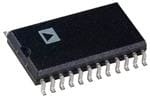
| 描述 | IC DAC VID 140MHZ 3.3/5V 24TSSOP视频 IC CMOS 240 MHz 10B High Speed DAC |
| 产品分类 | |
| 品牌 | Analog Devices Inc |
| 产品手册 | |
| 产品图片 |
|
| rohs | 符合RoHS无铅 / 符合限制有害物质指令(RoHS)规范要求 |
| 产品系列 | 多媒体 IC,视频 IC,Analog Devices ADV7127KRUZ140- |
| 数据手册 | |
| 产品型号 | ADV7127KRUZ140 |
| 产品培训模块 | http://www.digikey.cn/PTM/IndividualPTM.page?site=cn&lang=zhs&ptm=19145http://www.digikey.cn/PTM/IndividualPTM.page?site=cn&lang=zhs&ptm=18614http://www.digikey.cn/PTM/IndividualPTM.page?site=cn&lang=zhs&ptm=26125http://www.digikey.cn/PTM/IndividualPTM.page?site=cn&lang=zhs&ptm=26140http://www.digikey.cn/PTM/IndividualPTM.page?site=cn&lang=zhs&ptm=26150http://www.digikey.cn/PTM/IndividualPTM.page?site=cn&lang=zhs&ptm=26147 |
| 产品目录页面 | |
| 产品种类 | 视频 IC |
| 位数 | 10 |
| 供应商器件封装 | 24-TSSOP |
| 分辨率 | 10 bit |
| 包装 | 管件 |
| 商标 | Analog Devices |
| 安装类型 | 表面贴装 |
| 安装风格 | SMD/SMT |
| 封装 | Tube |
| 封装/外壳 | 24-TSSOP(0.173",4.40mm 宽) |
| 封装/箱体 | TSSOP-24 |
| 工作温度 | -40°C ~ 85°C |
| 工作电源电压 | 4.75 V to 5.25 V |
| 工厂包装数量 | 62 |
| 建立时间 | 15ns |
| 数据接口 | 并联 |
| 最大功率耗散 | 310 mW |
| 最大工作温度 | + 85 C |
| 最小工作温度 | - 40 C |
| 标准包装 | 62 |
| 电压源 | 单电源 |
| 类型 | Video Encoder |
| 系列 | ADV7127 |
| 转换器数 | 1 |
| 输出数和类型 | 2 电流,单极 |
| 通道数量 | 1 Channel |
| 采样率(每秒) | 240M |


PDF Datasheet 数据手册内容提取
CMOS, 240 MHz, 10-Bit, High Speed Video DAC Data Sheet ADV7127 FEATURES FUNCTIONAL BLOCK DIAGRAM 240 MSPS throughput rate VAA 10-bit digital-to-analog converter (DAC) RS-343A-/RS-170-compatible output 10 IOUT Complementary outputs D9 TO D0 DATA 10 DAC DAC output current range: 2 mA to 18.5 mA REGISTER IOUT TTL-compatible inputs Internal voltage reference PDOWN POWER-DOWN RVEOFLETRAEGNECE VREF PSAVE MODE CIRCUIT Single supply 5 V or 3.3 V operation 2Lo4w-le paodw tehrin d sishsriipnakt isomna ll outline package (TSSOP) package CLOCK GND RSET COMP ADV7127 14959-001 Low power standby mode Figure 1. Power-down mode Industrial temperature range (−40°C to +85°C) APPLICATIONS Digital video systems (1600 × 1200 at 100 Hz) High resolution color graphics Digital radio modulation Image processing Instrumentation Video signal reconstruction Direct digital synthesis (DDS) Wireless local area networks (LANs) GENERAL DESCRIPTION The ADV7127 is a high speed, DAC on a single monolithic PRODUCT HIGHLIGHTS chip. It consists of a 10-bit, video DAC with an on-board voltage 1. 240 MSPS throughput. reference, complementary outputs, a standard TTL input 2. Guaranteed monotonic to 10 bits. interface, and high impedance analog output current sources. 3. Compatible with a wide variety of high resolution color The ADV7127 has a 10-bit wide input port. A single 5 V or graphics systems including RS-343A and RS-170. 3.3 V power supply and clock are all that are required to make the device functional. The ADV7127 is fabricated in a complementary metal-oxide semiconductor (CMOS) process. Its monolithic CMOS construction ensures greater functionality with low power dissipation. The ADV7127 is available in a 24-lead TSSOP package which includes a power-down mode and an on-board voltage reference circuit. Rev. A Document Feedback Information furnished by Analog Devices is believed to be accurate and reliable. However, no responsibility is assumed by Analog Devices for its use, nor for any infringements of patents or other One Technology Way, P.O. Box 9106, Norwood, MA 02062-9106, U.S.A. rights of third parties that may result from its use. Specifications subject to change without notice. No license is granted by implication or otherwise under any patent or patent rights of Analog Devices. Tel: 781.329.4700 ©1998–2017 Analog Devices, Inc. All rights reserved. Trademarks and registered trademarks are the property of their respective owners. Technical Support www.analog.com
ADV7127 Data Sheet TABLE OF CONTENTS Features .............................................................................................. 1 Theory of Operation ...................................................................... 14 Applications ....................................................................................... 1 Digital Inputs .............................................................................. 14 Functional Block Diagram .............................................................. 1 Clock Input.................................................................................. 14 General Description ......................................................................... 1 Reference Input ........................................................................... 14 Product Highlights ........................................................................... 1 Digital-to-Analog Converter .................................................... 14 Revision History ............................................................................... 2 Analog Output ............................................................................ 15 Specifications ..................................................................................... 3 Gray Scale Operation ................................................................. 15 5 V Electrical Characteristics ...................................................... 3 Video Output Buffer .................................................................. 15 3.3 V Electrical Characteristics ................................................... 4 PCB Layout Considerations ...................................................... 16 5 V Timing Specifications ........................................................... 5 Ground Planes ............................................................................ 16 3.3 V Timing Specifications ........................................................ 6 Power Planes ............................................................................... 16 Absolute Maximum Ratings ............................................................ 7 Supply Decoupling ..................................................................... 16 ESD Caution .................................................................................. 7 Digital Signal Interconnect ....................................................... 16 Pin Configurations and Function Descriptions ........................... 8 Analog Signal Interconnect....................................................... 16 Typical Performance Characteristics ............................................. 9 Outline Dimensions ....................................................................... 18 5 V .................................................................................................. 9 Ordering Guide .......................................................................... 18 3.3 V ............................................................................................. 11 Terminology .................................................................................... 13 REVISION HISTORY 1/2017—Rev. 0 to Rev. A Changes to Figure 10 to Figure 12 ................................................ 10 Updated Format .................................................................. Universal Changes to Figure 18 Caption ...................................................... 11 Deleted SOIC_W Package ................................................. Universal Deleted Power Management Section and Table II ..................... 12 Change RS-170A to RS-170 ......................................... Throughout Changes to Figure 19 to Figure 21 ................................................ 12 Changes to Features Section............................................................ 1 Changed Circuit Description and Operation Section to Theory Deleted 5 V SOIC Specifications Table .......................................... 2 of Operation Section ...................................................................... 14 Changes to Table 1 ............................................................................ 3 Changes to Video Output Buffer Section .................................... 15 Deleted 3.3 V SOIC Specifications Table ....................................... 4 Changes to Supply Decoupling Section and Analog Signal Changes to Table 2 ............................................................................ 4 Interconnect Section ...................................................................... 16 Changes to Table 3 ............................................................................ 5 Updated Outline Dimensions ....................................................... 18 Deleted 5 V/3.3 V Dynamic Specifications Table ........................ 6 Changes to Ordering Guide .......................................................... 18 Changes to Table 4 ............................................................................ 6 Changes to Table 6 ............................................................................ 8 4/1998—Revision 0: Initial Version Changes to Figure 9 Caption ........................................................... 9 Rev. A | Page 2 of 18
Data Sheet ADV7127 SPECIFICATIONS 5 V ELECTRICAL CHARACTERISTICS V = 5 V ± 5%, V = 1.235 V, R = 560 Ω, C = 10 pF. All specifications T to T ,1 unless otherwise noted. T = 110°C. AA REF SET L MIN MAX J MAX Table 1. Parameter Symbol Min Typ Max Unit Test Conditions/Comments STATIC PERFORMANCE Resolution (Each DAC) 10 Bits Integral Nonlinearity (INL) –1 +0.4 +1 LSB Differential Nonlinearity –1 +0.25 +1 LSB Guaranteed monotonic DIGITAL AND CONTROL INPUTS Input Voltage High V 2 V IH Low V 0.8 V IL PDOWN Input Voltage High 3 V Low 1 V Input Current I –1 +1 µA V = 0.0 V or V IN IN AA Pull-Up Current PSAVE 20 µA PDOWN 20 µA Input Capacitance C 10 pF IN ANALOG OUTPUTS Output Current 2.0 18.5 mA Output Compliance Range V 0 1.4 V OC Output Impedance R 100 kΩ OUT Output Capacitance C 10 pF I = 0 mA OUT OUT Offset Error –0.025 +0.025 % FSR Tested with DAC output = 0 V Gain Error2 –5.0 +5.0 % FSR FSR = 17.62 mA VOLTAGE REFERENCE (EXTERNAL AND INTERNAL)3 Reference Range V 1.12 1.235 1.35 V REF POWER DISSIPATION Supply Current Digital 1.5 3 mA f = 50 MHz CLK 4 6 mA f = 140 MHz CLK 6.5 10 mA f = 240 MHz CLK Analog 23 27 mA R = 560 Ω SET 5 mA R = 4933 Ω SET Standby4 3.8 6 mA PSAVE = low, digital and control inputs at VAA PDOWN 1 mA Power Supply Rejection Ratio PSRR 0.1 0.5 %/% 1 Temperature range TMIN to TMAX: −40°C to +85°C at 50 MHz and 140 MHz, and 0°C to 70°C at 240 MHz. 2 Gain error = ((Measured (FSC)/Ideal (FSC) − 1) × 100), where Ideal = VREF/RSET × K × (0x3FF) and K = 7.9896. 3 The digital supply is measured with a continuous clock, with data input corresponding to a ramp pattern, and with an input level at 0 V and VDD. 4 These typical/maximum specifications are guaranteed by characterization to be over the 4.75 V to 5.25 V range. Rev. A | Page 3 of 18
ADV7127 Data Sheet 3.3 V ELECTRICAL CHARACTERISTICS V = 3.0 V to 3.6 V, V = 1.235 V, R = 560 Ω, C = 10 pF. All specifications T to T ,1 unless otherwise noted. T = 110°C. AA REF SET L MIN MAX J MAX Table 2. Parameter2 Symbol Min Typ Max Unit Test Conditions/Comments STATIC PERFORMANCE R = 680 Ω SET Resolution (Each DAC) 10 Bits Integral Nonlinearity (INL) –1 +0.5 +1 LSB Differential Nonlinearity –1 +0.25 +1 LSB DIGITAL AND CONTROL INPUTS Input Voltage High V 2.0 V IH Low V 0.8 V IL PDOWN Input Voltage High 2.1 V Low 0.6 V Input Current I –1 +1 μA V = 0.0 V or V IN IN DD PSAVE Pull-Up Current 20 μA Input Capacitance C 10 pF IN ANALOG OUTPUTS Output Current 2.0 18.5 mA Output Compliance Range V 0 1.4 V OC Output Impedance R 70 kΩ OUT Output Capacitance C 10 pF OUT Offset Error 0 0 % FSR Tested with DAC output = 0 V Gain Error3 0 % FSR FSR = 17.62 mA VOLTAGE REFERENCE (EXTERNAL) Reference Range V 1.12 1.235 1.35 V REF VOLTAGE REFERENCE (INTERNAL) Reference Range V 1.235 V REF POWER DISSIPATION Supply Current Digital4 1 2 mA f = 50 MHz CLK 2.5 4.5 mA f = 140 MHz CLK 4 6 mA f = 240 MHz CLK Analog 22 25 mA R = 560 Ω SET 5 mA R = 4933 Ω SET Standby 2.6 3 mA PSAVE = low, digital and control inputs at V DD PDOWN 20 μA Power Supply Rejection Ratio PSRR 0.1 0.5 %/% 1 Temperature range TMIN to TMAX: −40°C to +85°C at 50 MHz and 140 MHz and 0°C to 70°C at 240 MHz. 2 These maximum/minimum specifications are guaranteed by characterization to be over 3.0 V to 3.6 V range. 3 Gain error = ((Measured (FSC)/Ideal (FSC) − 1) × 100), where Ideal = VREF/RSET × K × (0x3FF) and K = 7.9896. 4 The digital supply is measured with a continuous clock, with data input corresponding to a ramp pattern, and with an input level at 0 V and VDD. Rev. A | Page 4 of 18
Data Sheet ADV7127 5 V TIMING SPECIFICATIONS V = 5 V ± 5%,1 V = 1.235 V, R = 560 Ω, C = 10 pF. All specifications T to T ,2 unless otherwise noted. T = 110°C. AA REF SET L MIN MAX J MAX Table 3. Parameter3 Symbol Min Typ Max Unit Test Conditions/Comments ANALOG OUTPUTS Delay t 5.5 ns 6 Rise/Fall Time4 t 1.0 ns 7 Transition Time5 t 15 ns 8 Skew6 t 1 2 ns Not shown in Figure 2 9 CLOCK CONTROL7 f 0.5 50 MHz 50 MHz grade CLK 0.5 140 MHz 140 MHz grade 0.5 240 MHz 240 MHz grade Data and Control Setup t 1.5 ns 1 Hold t 2.5 ns 2 Clock Pulse Width High t 1.875 1.1 ns f = 240 MHz 4 MAX 2.85 ns f = 140 MHz MAX 8.0 ns f = 50 MHz MAX Low t 1.875 1.25 ns f = 240 MHz 5 MAX 2.85 ns f = 140 MHz MAX 8.0 ns f = 50 MHz MAX Pipeline Delay6 t 1.0 1.0 1.0 Clock cycles Not shown in Figure 2 PD Up Time PSAVE6 t10 2 10 ns Not shown in Figure 2 PDOWN t11 320 ns Not shown in Figure 2 1 Maximum and minimum specifications are guaranteed over this range in Table 3. 2 Temperature range: TMIN to TMAX: −40°C to +85°C at 50 MHz and 140 MHz, and 0°C to 70°C at 240 MHz. 3 Timing specifications are measured with input levels of 3.0 V (VIH) and 0 V (VIL) for both 5 V and 3.3 V supplies. 4 Rise time was measured from the 10% to 90% point of zero to full-scale transition, and fall time from the 90% to 10% point of a full-scale transition. 5 Measured from 50% point of full-scale transition to 2% of final value. 6 Guaranteed by characterization. 7 fCLK maximum specification production tested at 125 MHz and 5 V. Limits specified in Table 3 are guaranteed by characterization. Rev. A | Page 5 of 18
ADV7127 Data Sheet 3.3 V TIMING SPECIFICATIONS V = 3.0 V to 3.6 V,1 V = 1.235 V, R = 560 Ω. All specifications T to T ,2 unless otherwise noted. T = 110°C. AA REF SET MIN MAX J MAX Table 4. Parameter3 Symbol Min Typ Max Unit Test Conditions/Comments ANALOG OUTPUTS Delay t 7.5 ns 6 Rise/Fall Time4 t 1.0 ns 7 Transition Time5 t 15 ns 8 Skew6 t 1 2 ns Not shown in Figure 2 9 CLOCK CONTROL7 f 50 MHz 50 MHz grade CLK 140 MHz 140 MHz grade 240 MHz 240 MHz grade Data and Control Setup6 t 1.5 ns 1 Hold6 t 2.5 ns 2 Clock Period6 t 2.5 ns f = 240 MHz 3 MAX Clock Pulse Width High t 1.1 ns f = 240 MHz 4 MAX t6 2.85 ns f = 140 MHz 4 MAX t6 8.0 ns f = 50 MHz 4 MAX Low6 t 1.4 ns f = 240 MHz 5 MAX t 2.85 ns f = 140 MHz 5 MAX t 8.0 ns f = 50 MHz 5 MAX Pipeline Delay6 t 1.0 1.0 1.0 Clock cycles Not shown in Figure 2 PD Up Time PSAVE6 t10 4 10 ns Not shown in Figure 2 PDOWN t11 320 ns Not shown in Figure 2 1 The values stated in Table 4 were obtained using VAA in the range of 3.0 V to 3.6 V. 2 Temperature range: TMIN to TMAX: −40°C to +85°C at 50 MHz and 140 MHz, and 0°C to 70°C at 240 MHz. 3 Timing specifications are measured with input levels of 3.0 V (VIH) and 0 V (VIL) for both 5 V and 3.3 V supplies. 4 Rise time was measured from the 10% to 90% point of zero to full-scale transition, and fall time from the 90% to 10% point of a full-scale transition. 5 Measured from 50% point of full-scale transition to 2% of final value. 6 Guaranteed by characterization. 7 fCLK maximum specification production tested at 125 MHz and 3.3 V. Limits specified in Table 4 are guaranteed by characterization. t3 t4 t5 CLOCK t2 DIGITAL INPUTS D9 TO D0 DATA t1 t8 ANALOG OUTPUTS t6 IOUT, IOUT t7 NOTES 1. OUTPUT DELAY (t6) MEASURED FROM THE 50% POINT OF THE RISING EDGE OF CLOCK TO THE 50% POINT OF FULL-SCALE TRANSITION. 2. OUTPUT RISE/FALL TIME (t7) MEASURED BETWEEN THE 10% AND 3 . T9T0RR%AA NNPSSOIITTINIIOOTSNN OTTIOFM FEWU (ItLT8LH) -IMSNCE 2AA%SL EUO RFTE RTDAH NFESR FIOTINMIOA TNLH .OEU 5T0P%U TP OVIANLTU OEF. FULL-SCALE 14959-002 Figure 2. Timing Diagram Rev. A | Page 6 of 18
Data Sheet ADV7127 ABSOLUTE MAXIMUM RATINGS Table 5. Stresses at or above those listed under Absolute Maximum Parameter Rating Ratings may cause permanent damage to the product. This is a V to GND 7 V stress rating only; functional operation of the product at these AA Voltage on Any Digital Pin GND − 0.5 V to V + 0.5 V or any other conditions above those indicated in the operational AA Ambient Operating Temperature Range −40°C to +85°C section of this specification is not implied. Operation beyond (TA) the maximum operating conditions for extended periods may Storage Temperature Range(TS) −65°C to +150°C affect product reliability. Junction Temperature (T) 150°C J ESD CAUTION Lead Temperature (Soldering, 10 sec) 300°C Vapor Phase Soldering (1 Minute) 220°C I to GND1 0 V to V OUT AA 1 Analog output short circuit to any power supply or common can be of an indefinite duration. Rev. A | Page 7 of 18
ADV7127 Data Sheet PIN CONFIGURATIONS AND FUNCTION DESCRIPTIONS D1 1 24 D0 D2 2 23 PSAVE D3 3 22 RSET D4 4 21 VREF D5 5 20 COMP D6 6 ADV7127 19 IOUT TOP VIEW D7 7 (Not to Scale) 18 IOUT D8 8 17 VAA D9 9 16 GND VAA 10 15 GND PDOWN 11 14 CLOCK DNCD =N CDO1 N2OT CONNECT 13 DNC 14959-003 Figure 3. Pin Configuration Table 6. Pin Function Descriptions Pin No. Mnemonic Description 1 to 9, D0 to D9 Data Inputs (TTL-Compatible). Data is latched on the rising edge of CLOCK. D0 is the least significant data bit. 24 Unused data inputs are connected to either the regular printed circuit board (PCB) power or ground plane. Data inputs are red, green, or blue pixel inputs. 10, 17 V Analog Power Supply (5 V ± 5%). All V pins on the ADV7127 must be connected. AA AA 11 PDOWN Power-Down Control Pin. The ADV7127 completely powers down, including the voltage reference circuit, when PDOWN is low. 12, 13 DNC Do Not Connect. Do not connect to these pins. 14 CLOCK Clock Input (TTL-Compatible). The rising edge of CLOCK latches D0 to D9 where D0 to D9 can be red, green, or blue pixel data inputs (TTL-compatible). CLOCK is typically the pixel clock rate of the video system. CLOCK is driven by a dedicated TTL buffer. 15, 16 GND Ground. All GND pins must be connected. 18 I Differential Current Output. This pin is capable of directly driving a doubly terminated 75 Ω load. If not required, OUT this output is tied to ground. 19 I Current Output. This high impedance current source is capable of directly driving a doubly terminated 75 Ω coaxial OUT cable. 20 COMP Compensation Pin. COMP is a compensation pin for the internal reference amplifier. A 0.1 μF ceramic capacitor must be connected between COMP and V . AA 21 V Voltage Reference Input. An external 1.23 V voltage reference must be connected to this pin. The use of an external REF resistor divider network is not recommended. A 0.1 μF decoupling ceramic capacitor is connected between V REF and V . AA 22 R Full-Scale Adjust Control. A resistor (R ) connected between this pin and GND controls the magnitude of the full- SET SET scale video signal. Note that the IRE relationships are maintained, regardless of the full-scale output current. The relationship between R and the full-scale output current on I is given by I (mA) = 7968 × V (V)/R (Ω). SET OUT OUT REF SET 23 PSAVE Power Save Control Pin. The device is put into standby mode when PSAVE is low. The internal voltage reference circuit is still active. Rev. A | Page 8 of 18
Data Sheet ADV7127 TYPICAL PERFORMANCE CHARACTERISTICS 5 V V = 5 V, V = 1.235 V, I = 17.62 µA, 50 Ω doubly terminated load, differential output loading, T = 25°C, unless otherwise noted. AA REF OUT A 70 76 SFDR (DIFFERENTIAL) SECOND HARMONIC 74 60 72 50 THIRD HARMONIC 70 FOURTH HARMONIC Bc) 40 SFDR (SINGLE-ENDED) c) d B 68 DR ( D (d F 30 H 66 S T 64 20 62 10 60 00.10 1.00 OU2.T5P1UT FRE5.Q0U4ENCY2 (0M.2H0z) 40.40 100.00 14959-005 580 50 fCLOC1K00 (MHz) 140 160 14959-008 Figure 4. SFDR vs. Output Frequency (fOUT) at fCLOCK = 140 MHz (Single-Ended Figure 7. THD vs. fCLOCK at fOUT = 2 MHz (Second, Third, and Fourth Harmonics) and Differential) 80 1.0 70 SFDR (DIFFERENTIAL) 0.9 0.8 60 SFDR (SINGLE-ENDED) 0.7 s) Bc) 50 LSB0.6 DR (d 40 RITY (0.5 F A S 30 NE0.4 LI 0.3 20 0.2 10 0.1 00.10 1.00 OU2.T5P1UT FRE5Q.0U4ENCY2 (0M.2H0z) 40.40 100.00 14959-006 00 2.00 IOUT (mA) 17.62 20.00 14959-009 Figure 5. SFDR vs. Output Frequency (fOUT) at fCLOCK = 50 MHz (Single-Ended Figure 8. Linearity vs. IOUT and Differential) 72.2 1.0 72.0 0.75 71.8 0.5 71.6 c) B) dB 71.4 LS R ( R ( 0 1023 FD 71.2 RO S R –0.16 E 71.0 70.8 –0.5 70.6 70.4 TEMPERATURE (°C) 14959-007 –1.0 CODE (INL) 14959-010 Figure 6. SFDR vs. Temperature at fCLOCK = 50 MHz (fOUT = 1 MHz) Figure 9. Error vs. Code Rev. A | Page 9 of 18
ADV7127 Data Sheet –5 –5 2 VAA = 5V VAA = 5V m) c) B B R (d –45 R (d –45 D D SF SF 1 1 –85 0SkTHAzRT 35.0MHz 70.S0TMOHPz 14959-011 –85 0SkTHAzRT 35.0MHz 70.S0TMOHPz 14959-013 Figure 10. Single Tone SFDR at fCLOCK = 140 MHz (fOUT1 = 2 MHz) Figure 12. Dual Tone SFDR at fCLOCK = 140 MHz (fOUT1 = 13.5 MHz, fOUT2 = 14.5 MHz) –5 VAA = 5V 2 m) B d R ( –45 D F S 1 –85 0SkTHAzRT 35.0MHz 70.S0TMOHPz 14959-012 Figure 11. Single Tone SFDR at fCLOCK = 140 MHz (fOUT1 = 20 MHz) Rev. A | Page 10 of 18
Data Sheet ADV7127 3.3 V V = 3 V, V = 1.235 V, I = 17.62 µA, 50 Ω doubly terminated load, differential output loading, T = 25°C, unless otherwise noted. AA REF OUT A 70 76 SECOND HARMONIC SFDR (DIFFERENTIAL) 74 60 FOURTHHARMONIC 72 50 70 SFDR (SINGLE-ENDED) THIRDHARMONIC SFDR (dBc) 4300 THD (dBc) 666846 20 62 60 10 58 00.10 2.51 O5U.T0P4UT FR2E0Q.2U0ENCY4 (0M.4H0z) 100.00 14959-014 560 50OUTPUT FRE10Q0UENCY (MHz)140 160 14959-017 Figure 13. SFDR vs. Output Frequency (fOUT) at fCLOCK = 140 MHz (Single-Ended Figure 16. THD vs. fCLOCK at Output Frequency and Differential) fOUT = 2 MHz (Second, Third, and Fourth Harmonics) 80 1.0 SFDR (DIFFERENTIAL) 70 0.9 SFDR (SINGLE-ENDED) 0.8 60 0.7 s) Bc) 50 LSB 0.6 R (d 40 TY ( 0.5 D RI SF 30 NEA 0.4 LI 0.3 20 0.2 10 0.1 00.1 0.10 OU2.T5P1UT FRE5.Q04UENCY2 (0M.2H0z) 40.40 100.00 14959-015 00 2.00 IOUT (mA) 17.62 20.00 14959-018 Figure 14. SFDR vs. Output Frequency (fOUT) at fCLOCK = 50 MHz (Single-Ended Figure 17. Linearity vs. IOUT and Differential) 72.0 1.0 71.8 0.75 71.6 0.5 c) 71.4 B) B S DR (d 71.2 OR (L 0 1023 SF 71.0 ERR –0.42 70.8 –0.5 70.6 70.40 20 TEMPER8A5TURE(°C) 145 165 14959-016 –1.0 CODE (INL) 14959-019 Figure 15. SFDR vs. Temperature at fCLOCK = 50 MHz, (fOUT = 1 MHz) Figure 18. Error vs. Code Rev. A | Page 11 of 18
ADV7127 Data Sheet –5 –5 2 VAA = 3.3V 2 VAA = 3.3V m) m) B B d d R (–45 R (–45 D D F F S S 1 1 –850SkTHAzRT 35.0MHz 70.S0TMOHPz 14959-020 –85 0SkTHAzRT 35.0MHz 70.S0MTOHPz 14959-022 Figure 19. Single Tone SFDR at fCLOCK = 140 MHz (fOUT1 = 2 MHz) Figure 21. Dual Tone SFDR at fCLOCK = 140 MHz (fOUT1 = 13.5 MHz, fOUT2 = 14.5 MHz) –5 VAA = 3.3V 2 m) B d R (–45 D F S 1 –85 0SkTHAzRT 35.0MHz 70.S0MTOHPz 14959-021 Figure 20. Single Tone SFDR at fCLOCK = 140 MHz (fOUT1 = 20 MHz) Rev. A | Page 12 of 18
Data Sheet ADV7127 TERMINOLOGY Color Video (RGB) Reference Black Level Color video (RGB) usually refers to the technique of combining Reference black level is the maximum negative polarity the three primary colors of red, green, and blue to produce color amplitude of the video signal. pictures within the usual spectrum. In RGB monitors, three DACs Reference White Level are required, one for each color. Reference white level is the maximum positive polarity Gray Scale amplitude of the video signal. Gray scale is the discrete levels of video signal between the Video Signal reference black and reference white levels. A 10-bit DAC Video signal is the portion of the composite video signal that varies contains 1024 different levels, whereas an 8-bit DAC contains 256. in gray scale levels between reference white and reference black. Raster Scan It is also referred to as the picture signal, which is the portion Raster scan is the most basic method of sweeping a CRT one that can be visually observed. line at a time to generate and display images. Rev. A | Page 13 of 18
ADV7127 Data Sheet THEORY OF OPERATION The ADV7127 contains one 10-bit DAC, with one input IOUT channel containing a 10-bit register. A reference amplifier is mA V also integrated on board the device. 17.61 0.66 WHITE LEVEL DIGITAL INPUTS Ten bits of data (color information), D0 to D9, are latched into the device on the rising edge of each clock cycle. This data is 100 IRE presented to the 10-bit DAC and is then converted to an analog output waveform (see Figure 22). 0 0 BLELVAECLK 14959-024 CLOCK Figure 23. IOUT RS-343A Video Output Waveform Table 7. Video Output Truth Table (R = 560 Ω, R = SET LOAD DIGITAL INPUTS D0 TO D9 DATA 37.5 Ω) Description Data IOUT (Ω) IOUT (Ω) DAC Input White Level 17.62 0 0x3FF ANALOG OIOUUTT,P IUOTUST 14959-023 VBildaceko Level 0V ideo 1177..6622 − Video D0xa0ta0 0 Figure 22. Video Data Input/Output All of these digital inputs are specified to accept TTL logic levels. REFERENCE INPUT CLOCK INPUT The ADV7127 has an on-board voltage reference. The V pin REF is normally terminated to V through a 0.1 µF capacitor. The CLOCK input of the ADV7127 is typically the pixel clock AA Alternatively, the device can, if required, be overdriven by an rate of the system. It is also known as the dot rate. The dot rate, external 1.23 V reference (AD1580). and therefore the required CLOCK frequency, is determined by the onscreen resolution, according to the following equation: A resistance RSET connected between the RSET pin and the GND pin determines the amplitude of the output video level according to Dot Rate = (Horizontal Resolution × Vertical Resolution × the following equation: Refresh Rate)/Retrace Factor I (mA) = (7968 × V (V))/R (Ω) where: OUT REF SET Horizontal Resolution is the number of pixels per line. Using a variable value of RSET allows accurate adjustment of the Vertical Resolution is the number of lines per frame. analog output video levels. Use of a fixed 560 Ω RSET resistor Refresh Rate is the horizontal scan rate at which the screen must yields the analog output levels quoted in Specifications section. be refreshed, typically 60 Hz for a noninterlaced system or These values typically correspond to the RS-343A video 30 Hz for an interlaced system. waveform values shown in Figure 23. Retrace Factor is the total blank time factor, which takes into DIGITAL-TO-ANALOG CONVERTER account that the display is blanked for a certain fraction of the The ADV7127 contains a 10-bit DAC. The DAC is designed using total duration of each frame (for example, 0.8). an advanced, high speed, segmented architecture. The bit currents If there is a graphics system with a 1024 × 1024 resolution, a corresponding to each digital input are routed to either the analog noninterlaced 60 Hz refresh rate, and a retrace factor of 0.8, then output (bit = 1) or GND (bit = 0) by a sophisticated decoding Dot Rate = (1024 × 1024 × 60)/0.8 = 78.6 MHz scheme. The use of identical current sources in a monolithic design guarantees monotonicity and low glitch. The on-board operational The required CLOCK frequency is 78.6 MHz. amplifier stabilizes the full-scale output current against temperature All video data and control inputs are latched into the ADV7127 on and power supply variations. the rising edge of CLOCK, as previously described in the Digital Inputs section. It is recommended that the CLOCK input to the ADV7127 be driven by a TTL buffer (for example, 74F244). Rev. A | Page 14 of 18
Data Sheet ADV7127 ANALOG OUTPUT More detailed information regarding load terminations for various output configurations, including RS-343A and RS-170, The analog output of the ADV7127 is a high impedance current is available in the AN-205 Application Note, Video Formats and source. The current output is capable of directly driving a 37.5 Ω Required Load Terminations. load, such as a doubly terminated 75 Ω coaxial cable. Figure 24 shows the required configuration for the output connected into Figure 23 shows the video waveforms associated with the a doubly terminated 75 Ω load. This arrangement develops current output driving the doubly terminated 75 Ω load of RS-343A video output voltage levels across a 75 Ω monitor. Figure 24. IOUT GRAY SCALE OPERATION ZO = 75Ω DAC The ADV7127 can be used for standalone, gray scale (mono- (CABLE) ZS = 75Ω ZL= 75Ω chrome), or composite video applications (that is, only one (SOURCE (MONITOR) channel used for video information). TERMINATION) 14959-025 VIDEO OUTPUT BUFFER The ADV7127 is specified to drive transmission line loads, which is Figure 24. Analog Output Termination for RS-343A what most monitors are rated as. The analog output configurations A suggested method of driving RS-170 video levels into a 75 Ω to drive such loads are shown in Figure 26. However, in some monitor is shown in Figure 25. The output current level of the applications, it may be required to drive long transmission line DAC remains unchanged, but the source termination resistance, cable lengths. Cable lengths greater than 10 meters can attenuate ZS, on the DAC is increased from 75 Ω to 150 Ω. and distort high frequency analog output pulses. The inclusion of IOUT the output buffers compensates for some cable distortion. Buffers ZO = 75Ω DAC with large full power bandwidths and gains between two and four (CABLE) are required. These buffers need to be able to supply sufficient Z(SS O =U 1R5C0ΩE ZL= 75Ω current over the complete output voltage swing. Analog Devices, (MONITOR) TERMINATION) Inc., produces a range of suitable op amps for such applications. 14959-026 Tamhepsse. Iinnc vluerdye hthigeh A frDe8q4u3e/nAcyD a8p4p4l/iAcaDti8o4n7s s(8er0i eMs oHf zm), othneo lAithDi8c 0o6p1 Figure 25. Analog Output Termination for RS-170 is recommended. More information on line driver buffering circuits is given in the relevant op amp data sheets. Use of buffer amplifiers also allows implementation of other video standards besides RS-343A and RS-170. Altering the gain components of the buffer circuit results in any desired video level. Z2 Z1 +VS 0.1µF IOUT 75Ω ZO = 75Ω AD848 DAC 0.1µF (CABLE) ZL = 75Ω (MONITOR) TERM(ISZNOSA UT= IR7OC5NΩE) –VS GAIN (G) = 1 +ZZ12 14959-027 Figure 26. AD848 As an Output Buffer Rev. A | Page 15 of 18
ADV7127 Data Sheet PCB LAYOUT CONSIDERATIONS SUPPLY DECOUPLING The ADV7127 is optimally designed for lowest noise perfor- Noise on the analog power plane can be further reduced by the mance, both radiated and conducted noise. To complement the use of multiple decoupling capacitors (see Figure 27). excellent noise performance of the ADV7127, it is imperative Optimum performance is achieved by the use of 0.1 µF ceramic that great care be given to the PCB layout. Figure 27 shows a capacitors. Each of the two groups of V is individually AA recommended connection diagram for the ADV7127. decoupled to ground. The V pins (Pin 10 and Pin 17) must be AA The PCB layout is optimized for lowest noise on the ADV7127 decoupled with capacitors to GND. Decouple the pins by power and ground lines. Radiated and conducted noise can be placing the capacitors as close as possible to the device with the achieved by shielding the digital inputs and providing good capacitor leads as short as possible between the V and GND AA decoupling. The lead length between groups of V and GND pins, thus minimizing lead inductance. AA pins is minimized to inductive ringing. It is important to note that while the ADV7127 contains GROUND PLANES circuitry to reject power supply noise, this rejection decreases with frequency. If a high frequency switching power supply is The ADV7127 and associated analog circuitry have a separate used, the designer must pay close attention to reducing power ground plane referred to as the analog ground plane. This supply noise. A dc power supply filter (Murata BNX002) ground plane connects to the regular PCB ground plane at a provides an electromagnetic interface (EMI) suppression single point through a ferrite bead, as illustrated in Figure 27. between the switching power supply and the main PCB. The ferrite bead is located as close as possible (within 3 inches) Alternatively, consider using a 3-terminal voltage regulator. to the ADV7127. DIGITAL SIGNAL INTERCONNECT The analog ground plane encompasses all ADV7127 ground pins, voltage reference circuitry, power supply bypass circuitry, The digital signal lines to the ADV7127 must be isolated as the analog output traces, and any output amplifiers. The regular much as possible from the analog outputs and other analog PCB ground plane area encompasses all the digital signal traces, circuitry. Digital signal lines must not overlay the analog power excluding the ground pins, leading up to the ADV7127. plane. POWER PLANES Due to the high clock rates used, long clock lines to the ADV7127 must be avoided to minimize noise pickup. The PCB layout has two distinct power planes: one for analog circuitry and one for digital circuitry. The analog power plane Any active pull-up termination resistors for the digital inputs encompasses the ADV7127 (VAA) and all associated analog are connected to the regular PCB power plane (VCC) and not the circuitry. This power plane is connected to the regular PCB analog power plane. power plane (VCC) at a single point through a ferrite bead, as ANALOG SIGNAL INTERCONNECT illustrated in Figure 27. This bead is located within 3 inches of The ADV7127 is located as close as possible to the output the ADV7127. connectors, which minimizes noise pickup and reflections due The PCB power plane provides power to all digital logic on the to impedance mismatch. PCB, and the analog power plane provides power to all The video output signals overlay the ground plane and not the ADV7127 power pins, voltage reference circuitry, and any analog power plane, thereby maximizing the high frequency output amplifiers. The PCB power and ground planes do not power supply rejection. overlay portions of the analog power plane. Keeping the PCB power and ground planes from overlaying the analog power For optimum performance, the analog outputs each have a plane contributes to a reduction in plane to plane noise source termination resistance to ground of 75 Ω (doubly coupling. terminated 75 Ω configuration). This termination resistance must be as close as possible to the ADV7127 to minimize reflections. Additional information on PCB design is available in the AN-333 Application Note, Design and Layout of a Video Graphics System for Reduced EMI. Rev. A | Page 16 of 18
Data Sheet ADV7127 COMP C6 0.1µF ANALOG POWER PLANE VAA ADV7127 C3 C4 C5 0.1µF 0.1µF 0.1µF L1 (FERRITE BEAD) +5V (VCC) VREF VIDEO D0 C2 C1 DATA 10µF 33µF INPUTS D9 ANALOG GROUND PLANE GND GROUND RSET R1 L2 (FERRITE BEAD) PDOWN 560Ω 75Ω PSAVE RSET VIDEO CLOCK IOUT OUTPUT COMPONENT DESCRIPTION VENDOR PART NUMBER C1 33µF TANTALUM CAPACITOR C2 10µF TANTALUM C3, C4, C5, C6 0.1µF CERAMIC CAPACITOR L1, L2 FERRITE BEAD FAIR-RITE 274300111 OR MURATA BL01/02/03 RSRE1T 75560ΩΩ 1 %1% M MEETTAALL F FILILMM R REESSISISTTOORR DDAALLEE CCMMFF--5555CC 14959-028 Figure 27. Typical Connection Diagram and Component List Rev. A | Page 17 of 18
ADV7127 Data Sheet OUTLINE DIMENSIONS 7.90 7.80 7.70 24 13 4.50 4.40 4.30 6.40 BSC 1 12 PIN 1 0.65 1.20 BSC MAX 0.15 0.05 8° 0.75 0.30 SEATING 0.20 0° 0.60 0.19 PLANE 0.09 0.45 0.10 COPLANARITY COMPLIANT TO JEDEC STANDARDS MO-153-AD Figure 28. 24-Lead Thin Shrink Small Outline Package [TSSOP] (RU-24) Dimensions shown in millimeters ORDERING GUIDE Speed Model1 Options Temperature Range Package Description Package Option ADV7127JRUZ240 240 MHz 0°C to 70°C 24-Lead Thin Shrink Small Outline Package [TSSOP] RU-24 ADV7127KRUZ50 50 MHz −40°C to +85°C 24-Lead Thin Shrink Small Outline Package [TSSOP] RU-24 ADV7127KRUZ50-REEL 50 MHz −40°C to +85°C 24-Lead Thin Shrink Small Outline Package [TSSOP] RU-24 ADV7127KRUZ140 140 MHz −40°C to +85°C 24-Lead Thin Shrink Small Outline Package [TSSOP] RU-24 ADV7127KRU50 50 MHz −40°C to +85°C 24-Lead Thin Shrink Small Outline Package [TSSOP] RU-24 ADV7127KRU50-REEL 50 MHz −40°C to +85°C 24-Lead Thin Shrink Small Outline Package [TSSOP] RU-24 ADV7127KRU140 140 MHz −40°C to +85°C 24-Lead Thin Shrink Small Outline Package [TSSOP] RU-24 1 Z = RoHS Compliant Part. ©1998–2017 Analog Devices, Inc. All rights reserved. Trademarks and registered trademarks are the property of their respective owners. D14959-0-1/17(A) Rev. A | Page 18 of 18
Mouser Electronics Authorized Distributor Click to View Pricing, Inventory, Delivery & Lifecycle Information: A nalog Devices Inc.: ADV7127JRUZ240 ADV7127KRUZ140 ADV7127KRUZ50 ADV7127KRUZ50-REEL