ICGOO在线商城 > 集成电路(IC) > 数据采集 - 数模转换器 > LTC2601IDD#PBF

 Datasheet下载
- 型号: LTC2601IDD#PBF
- 制造商: LINEAR TECHNOLOGY
- 库位|库存: xxxx|xxxx
- 要求:
| 数量阶梯 | 香港交货 | 国内含税 |
| +xxxx | $xxxx | ¥xxxx |
查看当月历史价格
查看今年历史价格
LTC2601IDD#PBF产品简介:
ICGOO电子元器件商城为您提供LTC2601IDD#PBF由LINEAR TECHNOLOGY设计生产,在icgoo商城现货销售,并且可以通过原厂、代理商等渠道进行代购。 LTC2601IDD#PBF价格参考。LINEAR TECHNOLOGYLTC2601IDD#PBF封装/规格:数据采集 - 数模转换器, 16 位 数模转换器 1 10-DFN(3x3)。您可以下载LTC2601IDD#PBF参考资料、Datasheet数据手册功能说明书,资料中有LTC2601IDD#PBF 详细功能的应用电路图电压和使用方法及教程。
LTC2601IDD#PBF 是 Linear Technology(现为 Analog Devices)生产的一款 8 通道、12 位电压输出数模转换器(DAC)。其应用场景广泛,主要涉及需要精确控制和调节模拟信号的领域。以下是该型号的一些典型应用场景:

 1. 工业自动化与过程控制
   - 在工业控制系统中,LTC2601 可用于生成精确的模拟电压信号来控制执行器、阀门或电机的速度和位置。
   - 它可以作为 PID 控制器的一部分,将数字计算结果转换为模拟信号,以驱动外部设备。

 2. 测试与测量设备
   - LTC2601 能够在测试仪器(如信号发生器、数据采集系统)中提供高精度的信号输出。
   - 其多通道特性使其适合同时生成多个独立的测试信号,适用于多点校准或复杂波形生成。

 3. 通信系统
   - 在通信设备中,该 DAC 可用于生成调制信号或偏置电压。
   - 例如,在射频前端电路中,它可以用来调整功率放大器的偏置电流或电压。

 4. 医疗设备
   - 在医疗成像设备(如超声波、CT 扫描仪)中,LTC2601 可用于生成驱动传感器或激励信号的精确电压。
   - 它还可用于患者监护设备中的信号调理模块,确保输出信号的稳定性和准确性。

 5. 汽车电子
   - 在汽车电子控制系统中,LTC2601 可用于调节传感器的参考电压或生成控制信号。
   - 例如,在发动机管理系统中,它可用于生成喷油器或点火系统的控制信号。

 6. 消费电子产品
   - 在音频设备中,该 DAC 可用于将数字音频信号转换为模拟信号输出。
   - 其低功耗特性也使其适合便携式设备中的应用。

 7. 科学仪器
   - 在实验室环境中,LTC2601 可用于生成精确的基准电压或模拟实验条件所需的信号。
   - 它的多通道功能使其能够支持复杂的实验设置。

 特性优势
- 低功耗:适合电池供电或对功耗敏感的应用。
- 小封装尺寸:节省 PCB 空间,便于小型化设计。
- 高精度与稳定性:确保输出信号的准确性和一致性。
- 内置上电复位功能:简化系统设计,提高可靠性。

综上所述,LTC2601IDD#PBF 凭借其高性能和灵活性,适用于多种需要精确模拟信号生成的场景,尤其是在工业、医疗、通信和消费电子领域中表现出色。
| 参数 | 数值 |
| 产品目录 | 集成电路 (IC) |
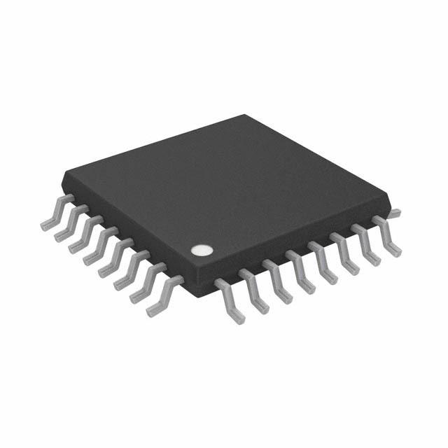
| 描述 | IC DAC 16BIT SGL R-R VOUT 10DFN |
| 产品分类 | |
| 品牌 | Linear Technology |
| 数据手册 | http://www.linear.com/docs/2796 |
| 产品图片 |
|
| 产品型号 | LTC2601IDD#PBF |
| rohs | 无铅 / 符合限制有害物质指令(RoHS)规范要求 |
| 产品系列 | - |
| 位数 | 16 |
| 供应商器件封装 | 10-DFN(3x3) |
| 其它名称 | LTC2601IDDPBF |
| 包装 | 管件 |
| 安装类型 | 表面贴装 |
| 封装/外壳 | 10-WFDFN 裸露焊盘 |
| 工作温度 | -40°C ~ 85°C |
| 建立时间 | 10µs |
| 数据接口 | 串行 |
| 标准包装 | 121 |
| 电压源 | 单电源 |
| 转换器数 | 1 |
| 输出数和类型 | 1 电压,单极 |
| 配用 | /product-detail/zh/DC777A/DC777A-ND/3029542 |
| 采样率(每秒) | * |


- 商务部:美国ITC正式对集成电路等产品启动337调查
- 曝三星4nm工艺存在良率问题 高通将骁龙8 Gen1或转产台积电
- 太阳诱电将投资9.5亿元在常州建新厂生产MLCC 预计2023年完工
- 英特尔发布欧洲新工厂建设计划 深化IDM 2.0 战略
- 台积电先进制程称霸业界 有大客户加持明年业绩稳了
- 达到5530亿美元!SIA预计今年全球半导体销售额将创下新高
- 英特尔拟将自动驾驶子公司Mobileye上市 估值或超500亿美元
- 三星加码芯片和SET,合并消费电子和移动部门,撤换高东真等 CEO
- 三星电子宣布重大人事变动 还合并消费电子和移动部门
- 海关总署:前11个月进口集成电路产品价值2.52万亿元 增长14.8%


PDF Datasheet 数据手册内容提取
LTC2601/LTC2611/LTC2621 16-/14-/12-Bit Rail-to-Rail DACs in 10-Lead DFN FEATURES DESCRIPTION n Smallest Pin-Compatible Single DACs: The LTC®2601/LTC2611/LTC2621 are single 16-, 14- and LTC2601: 16 Bits 12-bit, 2.5V-to-5.5V rail-to-rail voltage output DACs in a LTC2611: 14 Bits 10-lead DFN package. They have built-in high performance LTC2621: 12 Bits output buffers and are guaranteed monotonic. n Guaranteed Monotonic Over Temperature These parts establish new board-density benchmarks for n Wide 2.5V to 5.5V Supply Range 16- and 14-bit DACs and advance performance standards n Low Power Operation: 300μA at 3V for output drive and load regulation in single-supply, volt- n Power Down to 1μA, Max age-output DACs. n High Rail-to-Rail Output Drive (±15mA, Min) n Double-Buffered Data Latches The parts use a simple SPI/MICROWIRE compatible 3-wire n Asynchronous DAC Update Pin serial interface which can be operated at clock rates up to n LTC2601-1/LTC2611-1/LTC2621-1: Power-On Reset 50MHz. Daisy-chain capability, hardware CLR and asyn- to Midscale chronous DAC update (LDAC) pins are included. n Tiny (3mm × 3mm) 10-Lead DFN Package The LTC2601/LTC2611/LTC2621 incorporate a power-on reset circuit. During power-up, the voltage outputs rise APPLICATIONS less than 10mV above zero scale until a valid write and update take place. The power-on reset circuit resets the n Mobile Communications LTC2601-1/LTC2611-1/LTC2621-1 to midscale. The volt- n Process Control and Industrial Automation age outputs stay at midscale until a valid write and update n Instrumentation take place. n Automatic Test Equipment L, LT, LTC and LTM are registered trademarks of Linear Technology Corporation. All other trademarks are the property of their respective owners. Protected by U.S. Patents including 5396245. TYPICAL APPLICATION Differential Nonlinearity (LTC2601) 6 9 2 SDI REF VCC 1.0 VCC = 5V 0.8 VREF = 4.096V 0.6 SCK 0.4 3 B) 0.2 S 3S2H-BIFITT REINGPISUTTER REGDIASCTER 12-/14-/16-BIT DAC VOUT 7 DNL (L–0.02 REGISTER –0.4 –0.6 CS/LD –0.8 5 CONTROL DECODE –1.0 0 16384 32768 49152 65535 LOGIC CODE SDO 2600 TA01b 1 LDAC CLR GND 10 4 8 2601 TA01a 2601fb 1
LTC2601/LTC2611/LTC2621 ABSOLUTE MAXIMUM RATINGS PIN CONFIGURATION (Note 1) TOP VIEW Any Pin to GND ............................................–0.3V to 6V Any Pin to VCC..............................................–6V to 0.3V SDO 1 10 LDAC Maximum Junction Temperature...........................125°C SDI 2 9 VCC Storage Temperature Range ...................–65°C to 125°C SCK 3 11 8 GND CLR 4 7 VOUT Lead Temperature (Soldering, 10 sec) ..................300°C CS/LD 5 6 REF Operating Temperature Range: LTC2601C/LTC2611C/LTC2621C DD PACKAGE 10-LEAD (3mm (cid:115) 3mm) PLASTIC DFN LTC2601C-1/LTC2611C-1/LTC2621C-1 ....0°C to 70°C TJMAX = 125°C, θJA = 43°C/W EXPOSED PAD (PIN 11) IS GND, MUST BE SOLDERED TO PCB LTC2601I/LTC2611I/LTC2621I LTC2601I-1/LTC2611I-1/LTC2621I-1 ....–40°C to 85°C ORDER INFORMATION LEAD FREE FINISH TAPE AND REEL PART MARKING* PACKAGE DESCRIPTION TEMPERATURE RANGE LTC2601CDD#PBF LTC2601CDD#TRPBF LAGT 10-Lead (3mm × 3mm) Plastic DFN 0°C to 70°C LTC2601IDD#PBF LTC2601IDD#TRPBF LAGT 10-Lead (3mm × 3mm) Plastic DFN –40°C to 85°C LTC2611CDD#PBF LTC2611CDD#TRPBF LBFQ 10-Lead (3mm × 3mm) Plastic DFN 0°C to 70°C LTC2611IDD#PBF LTC2611IDD#TRPBF LBFQ 10-Lead (3mm × 3mm) Plastic DFN –40°C to 85°C LTC2621CDD#PBF LTC2621CDD#TRPBF LBFS 10-Lead (3mm × 3mm) Plastic DFN 0°C to 70°C LTC2621IDD#PBF LTC2621IDD#TRPBF LBFS 10-Lead (3mm × 3mm) Plastic DFN –40°C to 85°C LTC2601CDD-1#PBF LTC2601CDD-1#TRPBF LBZH 10-Lead (3mm × 3mm) Plastic DFN 0°C to 70°C LTC2601IDD-1#PBF LTC2601IDD-1#TRPBF LBZH 10-Lead (3mm × 3mm) Plastic DFN –40°C to 85°C LTC2611CDD-1#PBF LTC2611CDD-1#TRPBF LBZJ 10-Lead (3mm × 3mm) Plastic DFN 0°C to 70°C LTC2611IDD-1#PBF LTC2611IDD-1#TRPBF LBZJ 10-Lead (3mm × 3mm) Plastic DFN –40°C to 85°C LTC2621CDD-1#PBF LTC2621CDD-1#TRPBF LBZK 10-Lead (3mm × 3mm) Plastic DFN 0°C to 70°C LTC2621IDD-1#PBF LTC2621IDD-1#TRPBF LBZK 10-Lead (3mm × 3mm) Plastic DFN –40°C to 85°C LEAD BASED FINISH TAPE AND REEL PART MARKING* PACKAGE DESCRIPTION TEMPERATURE RANGE LTC2601CDD LTC2601CDD#TR LAGT 10-Lead (3mm × 3mm) Plastic DFN 0°C to 70°C LTC2601IDD LTC2601IDD#TR LAGT 10-Lead (3mm × 3mm) Plastic DFN –40°C to 85°C LTC2611CDD LTC2611CDD#TR LBFQ 10-Lead (3mm × 3mm) Plastic DFN 0°C to 70°C LTC2611IDD LTC2611IDD#TR LBFQ 10-Lead (3mm × 3mm) Plastic DFN –40°C to 85°C LTC2621CDD LTC2621CDD#TR LBFS 10-Lead (3mm × 3mm) Plastic DFN 0°C to 70°C LTC2621IDD LTC2621IDD#TR LBFS 10-Lead (3mm × 3mm) Plastic DFN –40°C to 85°C LTC2601CDD-1 LTC2601CDD-1#TR LBZH 10-Lead (3mm × 3mm) Plastic DFN 0°C to 70°C LTC2601IDD-1 LTC2601IDD-1#TR LBZH 10-Lead (3mm × 3mm) Plastic DFN –40°C to 85°C LTC2611CDD-1 LTC2611CDD-1#TR LBZJ 10-Lead (3mm × 3mm) Plastic DFN 0°C to 70°C LTC2611IDD-1 LTC2611IDD-1#TR LBZJ 10-Lead (3mm × 3mm) Plastic DFN –40°C to 85°C LTC2621CDD-1 LTC2621CDD-1#TR LBZK 10-Lead (3mm × 3mm) Plastic DFN 0°C to 70°C LTC2621IDD-1 LTC2621IDD-1#TR LBZK 10-Lead (3mm × 3mm) Plastic DFN –40°C to 85°C Consult LTC Marketing for parts specifi ed with wider operating temperature ranges. *The temperature grade is identifi ed by a label on the shipping container. For more information on lead free part marking, go to: http://www.linear.com/leadfree/ For more information on tape and reel specifi cations, go to: http://www.linear.com/tapeandreel/ 2601fb 2
LTC2601/LTC2611/LTC2621 ELECTRICAL CHARACTERISTICS The l denotes the specifi cations which apply over the full operating temperature range, otherwise specifi cations are at T = 25°C. REF = 4.096V (V = 5V), REF = 2.048V (V = 2.5V), V unloaded, A CC CC OUT unless otherwise noted. LTC2621/ LTC2621-1 LTC2611/ LTC2611-1 LTC2601/ LTC2601-1 SYMBOL PARAMETER CONDITIONS MIN TYP MAX MIN TYP MAX MIN TYP MAX UNITS DC Performance Resolution l 12 14 16 Bits Monotonicity (Note 2) l 12 14 16 Bits DNL Differential Nonlinearity (Note 2) l ±0.5 ±1 ±1 LSB INL Integral Nonlinearity (Note 2) l ±0.8 ±4 ±3 ±16 ±13 ±64 LSB Load Regulation V = V = 5V, Midscale REF CC I = 0mA to 15mA Sourcing l 0.03 0.125 0.10 0.5 0.45 2 LSB/mA OUT I = 0mA to 15mA Sinking l 0.04 0.125 0.15 0.5 0.60 2 LSB/mA OUT V = V = 2.5V, Midscale REF CC I = 0mA to 7.5mA Sourcing l 0.06 0.25 0.2 1 0.9 4 LSB/mA OUT I = 0mA to 7.5mA Sinking l 0.08 0.25 0.3 1 1.2 4 LSB/mA OUT ZSE Zero-Scale Error Code = 0 l 1 9 1 9 1 9 mV V Offset Error (Note 5) l ±1.5 ±9 ±1.5 ±9 ±1.5 ±9 mV OS V Temperature ±5 ±5 ±5 μV/°C OS Coeffi cient GE Gain Error l ±0.03 ±0.7 ±0.1 ±0.7 ±0.05 ±0.7 %FSR Gain Temperature ±2 ±2 ±2 ppm/°C Coeffi cient The l denotes the specifi cations which apply over the full operating temperature range, otherwise specifi cations are at T = 25°C. A REF = 4.096V (V = 5V), REF = 2.048V (V = 2.5V), V unloaded, unless otherwise noted. (Note 8) CC CC OUT SYMBOL PARAMETER CONDITIONS MIN TYP MAX UNITS PSR Power Supply Rejection V = 5V ±10% –80 dB CC V = 3V ±10% l –80 dB CC R DC Output Impedance V = V = 5V, Midscale; –15mA ≤ I ≤ 15mA l 0.04 0.15 Ω OUT REF CC OUT V = V = 2.5V, Midscale; –7.5mA ≤ I ≤ 7.5mA l 0.05 0.15 Ω REF CC OUT I Short-Circuit Output Current V = 5.5V, V = 5.5V SC CC REF Code: Zero Scale; Forcing Output to V l 15 35 60 mA CC Code: Full Scale; Forcing Output to GND l 15 39 60 mA V = 2.5V, V = 2.5V CC REF Code: Zero Scale; Forcing Output to V l 7.5 20 50 mA CC Code: Full Scale; Forcing Output to GND l 7.5 27 50 mA Reference Input Input Voltage Range l 0 VCC V Resistance Normal Mode l 88 124 160 kΩ Capacitance 15 pF I Reference Current, Power Down Mode DAC Powered Down l 0.001 1 μA REF Power Supply V Positive Supply Voltage For Specifi ed Performance l 2.5 5.5 V CC I Supply Current V = 5V (Note 3) l 0.375 0.55 mA CC CC V = 3V (Note 3) l 0.30 0.45 mA CC DAC Powered Down (Note 3) V = 5V l 0.40 1 μA CC DAC Powered Down (Note 3) V = 3V l 0.10 1 μA CC Digital I/O V Digital Input High Voltage V = 2.5V to 5.5V l 2.4 V IH CC V = 2.5V to 3.6V l 2.0 V CC 2601fb 3
LTC2601/LTC2611/LTC2621 ELECTRICAL CHARACTERISTICS The l denotes the specifi cations which apply over the full operating temperature range, otherwise specifi cations are at T = 25°C. REF = 4.096V (V = 5V), REF = 2.048V (V = 2.5V), V unloaded, A CC CC OUT unless otherwise noted. (Note 8) SYMBOL PARAMETER CONDITIONS MIN TYP MAX UNITS V Digital Input Low Voltage V = 4.5V to 5.5V l 0.8 V IL CC V = 2.5V to 5.5V l 0.6 V CC V Digital Output High Voltage Load Current = –100μA l V – 0.4 V OH CC V Digital Output Low Voltage Load Current = +100μA l 0.4 V OL I Digital Input Leakage V = GND to V l ±1 μA LK IN CC C Digital Input Capacitance (Note 4) l 8 pF IN The l denotes the specifi cations which apply over the full operating temperature range, otherwise specifi cations are at T = 25°C. A REF = 4.096V (V = 5V), REF = 2.048V (V = 2.5V), V unloaded, unless otherwise noted. CC CC OUT LTC2621/ LTC2621-1 LTC2611/ LTC2611-1 LTC2601/ LTC2601-1 SYMBOL PARAMETER CONDITIONS MIN TYP MAX MIN TYP MAX MIN TYP MAX UNITS AC Performance t Settling Time (Note 6) ±0.024% (±1LSB at 12 Bits) 7 7 7 μs S ±0.006% (±1LSB at 14 Bits) 9 9 μs ±0.0015% (±1LSB at 16 Bits) 10 μs Settling Time for 1LSB Step ±0.024% (±1LSB at 12 Bits) 2.7 2.7 2.7 μs (Note 7) ±0.006% (±1LSB at 14 Bits) 4.8 4.8 μs ±0.0015% (±1LSB at 16 Bits) 5.2 μs Voltage Output Slew Rate 0.80 0.80 0.80 V/μs Capacitive Load Driving 1000 1000 1000 pF Glitch Impulse At Midscale Transition 12 12 12 nV • s Multiplying Bandwidth 180 180 180 kHz e Output Voltage Noise At f = 1kHz 120 120 120 nV/√Hz n Density At f = 10kHz 100 100 100 nV/√Hz Output Voltage Noise 0.1Hz to 10Hz 15 15 15 μV P-P TIMING CHARACTERISTICS The l denotes the specifi cations which apply over the full operating temperature range, otherwise specifi cations are at T = 25°C. (See Figure 1) (Notes 4, 8) A SYMBOL PARAMETER CONDITIONS MIN TYP MAX UNITS V = 2.5V to 5.5V CC t SDI Valid to SCK Setup l 4 ns 1 t SDI Valid to SCK Hold l 4 ns 2 t SCK High Time l 9 ns 3 t SCK Low Time l 9 ns 4 t CS/LD Pulse Width l 10 ns 5 t LSB SCK High to CS/LD High l 7 ns 6 t CS/LD Low to SCK High l 7 ns 7 t SDO Propagation Delay from SCK Falling Edge C = 10pF 8 LOAD V = 4.5V to 5.5V l 20 ns CC V = 2.5V to 5.5V l 45 ns CC t CLR Pulse Width l 20 ns 9 t CS/LD High to SCK Positive Edge l 7 ns 10 t LDAC Pulse Width l 15 ns 12 t CS/LD High to LDAC High or Low Transition l 200 ns 13 SCK Frequency 50% Duty Cycle l 50 MHz 2601fb 4
LTC2601/LTC2611/LTC2621 TIMING CHARACTERISTICS Note 1: Stresses beyond those listed under Absolute Maximum Ratings Note 4: Guaranteed by design and not production tested. may cause permanent damage to the device. Exposure to any Absolute Note 5: Inferred from measurement at code K = 0.016(2N/V ) and at L REF Maximum Rating condition for extended periods may affect device full scale. reliability and lifetime. Note 6: V = 5V, V = 4.096V. DAC is stepped 1/4 scale to 3/4 scale and CC REF Note 2: Linearity and monotonicity are defi ned from code KL to code 3/4 scale to 1/4 scale. Load is 2k in parallel with 200pF to GND. 2N – 1, where N is the resolution and K is given by K = 0.016(2N/V ), L L REF Note 7: V = 5V, V = 4.096V. DAC is stepped ±1LSB between half scale CC REF rounded to the nearest whole code. For V = 4.096V and N = 16, K = REF L and half scale – 1. Load is 2k in parallel with 200pF to GND. 256 and linearity is defi ned from code 256 to code 65,535. Note 8: These specifi cations apply to LTC2601/LTC2601-1, Note 3: Digital inputs at 0V or V . CC LTC2611/LTC2611-1, LTC2621/LTC2621-1 TYPICAL PERFORMANCE CHARACTERISTICS LTC2601 Integral Nonlinearity (INL) Differential Nonlinearity (DNL) INL vs Temperature 32 1.0 32 VCC = 5V VCC = 5V VCC = 5V 24 VREF = 4.096V 0.8 VREF = 4.096V 24 VREF = 4.096V 0.6 16 16 0.4 8 8 INL (POS) NL (LSB) 0 NL (LSB) 0.20 NL (LSB) 0 I –8 D–0.2 I –8 INL (NEG) –0.4 –16 –16 –0.6 –24 –24 –0.8 –32 –1.0 –32 0 16384 32768 49152 65535 0 16384 32768 49152 65535 –50 –30 –10 10 30 50 70 90 CODE CODE TEMPERATURE (°C) 2601 G01 2600 G02 2601 G03 DNL vs Temperature INL vs V DNL vs V REF REF 1.0 32 1.5 VCC = 5V VCC = 5.5V VCC = 5.5V 0.8 VREF = 4.096V 24 1.0 0.6 16 0.4 DNL (POS) INL (POS) 0.5 8 DNL (LSB)–00..202 DNL (NEG) INL (LSB) –08 INL (NEG) DNL (LSB)–0.05 DDNNLL ((PNOEGS)) –0.4 –16 –0.6 –1.0 –24 –0.8 –1.0 –32 –1.5 –50 –30 –10 10 30 50 70 90 0 1 2 3 4 5 0 1 2 3 4 5 TEMPERATURE (°C) VREF (V) VREF (V) 2601 G04 2601 G05 2601 G06 2601fb 5
LTC2601/LTC2611/LTC2621 TYPICAL PERFORMANCE CHARACTERISTICS LTC2601 Settling to ±1LSB Settling of Full-Scale Step VOUT VOUT 100μV/DIV 100μV/DIV 12.3μs 9.7μs CS/LD CS/LD 2V/DIV 2V/DIV 2μs/DIV 2601 G07 5μs/DIV 2601 G08 VCC = 5V, VREF = 4.096V SETTLING TO ±1LSB 1/4-SCALE TO 3/4-SCALE STEP VCC = 5V, VREF = 4.096V RL = 2k, CL = 200pF CODE 512 TO 65535 STEP AVERAGE OF 2048 EVENTS AVERAGE OF 2048 EVENTS LTC2611 Integral Nonlinearity (INL) Differential Nonlinearity (DNL) Settling to ±1LSB 8 1.0 VCC = 5V VCC = 5V 6 VREF = 4.096V 0.8 VREF = 4.096V 0.6 4 0.4 2 VOUT INL (LSB) –02 DNL (LSB)–00..202 1002μCVVS//DD/LIIDVV 8.9μs –0.4 –4 –0.6 2μs/DIV 2601 G11 –6 –0.8 VCC = 5V, VREF = 4.096V 1/4-SCALE TO 3/4-SCALE STEP –8 –1.0 0 4096 8192 12288 16383 0 4096 8192 12288 16383 RL = 2k, CL = 200pF AVERAGE OF 2048 EVENTS CODE CODE 2601 G09 2601 G10 LTC2621 Integral Nonlinearity (INL) Differential Nonlinearity (DNL) Settling to ±1LSB 2.0 1.0 VCC = 5V VCC = 5V 1.5 VREF = 4.096V 0.8 VREF = 4.096V 0.6 1.0 6.8μs 0.4 0.5 VOUT INL (LSB)–0.05 DNL (LSB) –00..202 1m2CVVS//DD/LIIDVV –0.4 –1.0 –0.6 2μs/DIV 2601 G14 –1.5 –0.8 VCC = 5V, VREF = 4.096V 1/4-SCALE TO 3/4-SCALE STEP –2.0 –1.0 0 1024 2048 3072 4095 0 1024 2048 3072 4095 RL = 2k, CL = 200pF AVERAGE OF 2048 EVENTS CODE CODE 2601 G12 2601 G13 2601fb 6
LTC2601/LTC2611/LTC2621 TYPICAL PERFORMANCE CHARACTERISTICS LTC2601/LTC2611/LTC2621 Current Limiting Load Regulation Offset Error vs Temperature 0.10 1.0 3 CODE = MIDSCALE CODE = MIDSCALE 0.08 0.8 VREF = VCC = 5V 2 0.06 0.6 VREF = VCC = 3V 0.04 0.4 V) m 1 ΔV (V)OUT––000...0002024 VREF = VCC = 3V ΔV (mV)OUT ––000...2024 VREF = VCC = 5V OFFSET ERROR ( –01 VREF = VCC = 5V VREF = VCC = 3V –0.06 –0.6 –2 –0.08 –0.8 –0.10 –1.0 –3 –40 –30 –20 –10 0 10 20 30 40 –35 –25 –15 –5 5 15 25 35 –50 –30 –10 10 30 50 70 90 IOUT (mA) IOUT (mA) TEMPERATURE (°C) 2601 G17 2601 G18 2601 G19 Zero-Scale Error vs Temperature Gain Error vs Temperature Offset Error vs V CC 3 0.4 3 0.3 2.5 2 V) 0.2 SCALE ERROR (m 21..05 N ERROR (%FSR)–00..101 SET ERROR (mV) 10 O- 1.0 AI FF –1 R G O ZE –0.2 0.5 –2 –0.3 0 –0.4 –3 –50 –30 –10 10 30 50 70 90 –50 –30 –10 10 30 50 70 90 2.5 3 3.5 4 4.5 5 5.5 TEMPERATURE (°C) TEMPERATURE (°C) VCC (V) 2601 G20 2601 G21 2601 G22 Gain Error vs V I Shutdown vs V Large-Signal Response CC CC CC 0.4 450 0.3 400 0.2 350 R) S 300 %F 0.1 VOUT RROR ( 0 (nA)CC225000 0.5V/DIV AIN E–0.1 I 150 VREF = VCC = 5V G 1/4-SCALE TO 3/4-SCALE –0.2 100 –0.3 2.5μs/DIV 2601 G25 50 –0.4 0 2.5 3 3.5 4 4.5 5 5.5 2.5 3 3.5 4 4.5 5 5.5 VCC (V) VCC (V) 2601 G23 2601 G24 2601fb 7
LTC2601/LTC2611/LTC2621 TYPICAL PERFORMANCE CHARACTERISTICS LTC2601/LTC2611/LTC2621 Power-On Reset Glitch Headroom at Rails Midscale Glitch Impulse to Zero Scale vs Output Current 5.0 4.5 5V SOURCING 4.0 10mVV/ODUIVT VCC 3.5 1V/DIV 3V SOURCING 12nV-s TYP 3.0 V) (UT2.5 4mV PEAK O CS/LD V 2.0 5V/DIV VOUT 1.5 10mV/DIV 5V SINKING 1.0 2.5μs/DIV 2601 G26 250μs/DIV 2601 G27 3V SINKING 0.5 0 0 1 2 3 4 5 6 7 8 9 10 IOUT (mA) 2601 G28 Supply Current vs Logic Voltage Hardware CLR to Zero Scale Hardware CLR to Midscale 1.4 VCC = 5V VCC = 5V VCC = 5V 1.2 SWEEP SCK, SDI VREF = 4.096V VREF = 4.096V ANDCS/LD CODE = FULL SCALE VOUT CODE = FULL SCALE 0V TO VCC 1V/DIV 1.0 VOUT 1V/DIV A) 0.8 m (C C 0.6 I CLR CLR 0.4 5V/DIV 5V/DIV 0.2 1μs/DIV 2601 G31 1μs/DIV 2601 G34 0 0 0.5 1 1.5 2 2.5 3 3.5 4 4.5 5 LOGIC VOLTAGE (V) 2601 G29 Output Voltage Noise, Power-On Reset to Midscale Multiplying Bandwidth 0.1Hz to 10Hz 0 VREF = VCC –3 –6 –9 –12 1V/DIV –15 VOUT 10μV/DIV dB–18 VCC –21 –24 VOUT –27 VCC = 5V 500μs/DIV 2601 G35 –30 VREF (DC) = 2V 0 1 2 3 4 5 6 7 8 9 10 –33 VCROEDFE ( A=C F)U =L L0 .S2CVAP-LPE SECONDS –36 2601 G33 1k 10k 100k 1M FREQUENCY (Hz) 2601 G32 2601fb 8
LTC2601/LTC2611/LTC2621 TYPICAL PERFORMANCE CHARACTERISTICS LTC2601/LTC2611/LTC2621 Short-Circuit Output Current vs Short-Circuit Output Current vs V (Sinking) V (Sourcing) OUT OUT 50 0 VCC = 5.5V VCC = 5.5V VREF = 5.6V VREF = 5.6V 40 CODE = 0 –10 CODE = FULL SCALE VOUT SWEPT 0V TO VCC VOUT SWEPT VCC TO 0V V 30 V–20 DI DI A/ A/ m m 0 0 1 20 1–30 10 –40 0 –50 0 1 2 3 4 5 6 0 1 2 3 4 5 6 1V/DIV 1V/DIV 2601 G15 2601 G16 PIN FUNCTIONS SDO (Pin 1): Serial Interface Data Output. This pin is used CS/LD (Pin 5): Serial Interface Chip Select/Load Input. for daisy-chain operation. The serial output of the shift When CS/LD is low, SCK is enabled for shifting data on register appears at the SDO pin. The data transferred to SDI into the register. When CS/LD is taken high, SCK the device via the SDI pin is delayed 32 SCK rising edges is disabled and the specifi ed command (see Table 1) is before being output at the next falling edge. SDO is an executed. active output and does not go high impedance even when REF (Pin 6): Reference Voltage Input. 0V ≤ V ≤ V . REF CC CS/LD is taken to a logic high level. V (Pin 7): DAC Analog Voltage Output. The output OUT SDI (Pin 2): Serial Interface Data Input. Data is applied range is 0V to V . REF to SDI for transfer to the device at the rising edge of SCK (Pin 3). The LTC2601 accepts input word lengths of either GND (Pin 8): Analog Ground. 24 or 32 bits. V (Pin 9): Supply Voltage Input. 2.5V ≤ V ≤ 5.5V. CC CC SCK (Pin 3): Serial Interface Clock Input. CMOS and TTL LDAC (Pin 10): Asynchronous DAC Update Pin. If CS/LD compatible. is high, a falling edge on LDAC immediately updates the CLR (Pin 4): Asynchronous Clear Input. A logic low at this DAC register with the contents of the input register (similar level-triggered input clears all registers and causes the to a software update). If CS/LD is low when LDAC goes DAC voltage outputs to drop to 0V for LTC2601/LTC2611/ low, the DAC register is updated after CS/LD returns high. LTC2621. A logic low at this input sets all registers to A low on the LDAC pin powers up the DAC. A software midscale code and causes the DAC voltage outputs to go power down command is ignored if LDAC is low. to midscale for LTC2601-1/LTC2611-1/LTC2621-1. CMOS Exposed Pad (Pin 11): Ground. Must be soldered to PCB and TTL compatible. ground. 2601fb 9
LTC2601/LTC2611/LTC2621 BLOCK DIAGRAM 6 9 SDI REF VCC 2 SCK 3 32-BIT INPUT DAC VOUT SHIFT 12-/14-/16-BIT DAC 7 REGISTER REGISTER REGISTER CS/LD 5 CONTROL DECODE LOGIC SDO 1 LDAC CLR GND 10 4 8 2601 BD TIMING DIAGRAMS t1 t2 t3 t4 t6 SCK 1 2 3 23 24 t10 SDI t5 t7 CS/LD t8 SDO t13 t12 LDAC 2601 F01a Figure 1a CS/LD t13 LDAC 2601 F01b Figure 1b 2601fb 10
LTC2601/LTC2611/LTC2621 OPERATION Power-On Reset only be transferred to the device when the CS/LD signal is low.The rising edge of CS/LD ends the data transfer and The LTC2601/LTC2611/LTC2621 clear the outputs to zero causes the device to execute the command specifi ed in scale when power is fi rst applied, making system initializa- the 24-bit input word. The complete sequence is shown tion consistent and repeatable. The LTC2601-1/LTC2611- in Figure 2a. 1/LTC2621-1 set the voltage outputs to midscale when power is fi rst applied. The command (C3-C0) assignments are shown in Table 1. The fi rst four commands in the table consist of write For some applications, downstream circuits are active and update operations. A write operation loads a 16-bit during DAC power-up, and may be sensitive to nonzero data word from the 32-bit shift register into the input outputs from the DAC during this time. The LTC2601/ register of the DAC. In an update operation, the data word LTC2611/LTC2621 contain circuitry to reduce the power- is copied from the input register to the DAC register and on glitch; furthermore, the glitch amplitude can be made converted to an analog voltage at the DAC output. The arbitrarily small by reducing the ramp rate of the power update operation also powers up the DAC if it had been in supply. For example, if the power supply is ramped to 5V power-down mode. The data path and registers are shown in 1ms, the analog outputs rise less than 10mV above in the Block Diagram. ground (typ) during power-on. See Power-On Reset Glitch in the Typical Performance Characteristics section. While the minimum input word is 24 bits, it may option- ally be extended to 32 bits. To use the 32-bit word width, Power Supply Sequencing 8 don’t-care bits are transferred to the device fi rst, followed by the 24-bit word as just described. Figure 2b shows the The voltage at REF (Pin 6) should be kept within the range 32-bit sequence. The 32-bit word is required for daisy- –0.3V ≤ V ≤ V + 0.3V (see Absolute Maximum Rat- REF CC chain operation, and is also available to accommodate ings). Particular care should be taken to observe these microprocessors which have a minimum word width of limits during power supply turn-on and turn-off sequences, 16 bits (2 bytes). when the voltage at V (Pin 16) is in transition. CC Daisy-Chain Operation Transfer Function The serial output of the shift register appears at the SDO The digital-to-analog transfer function is: pin. Data transferred to the device from the SDI input is ⎛ k ⎞ V =⎜ ⎟V delayed 32 SCK rising edges before being output at the OUT(IDEAL) ⎝2N⎠ REF next SCK falling edge. where k is the decimal equivalent of the binary DAC input The SDO output can be used to facilitate control of multiple code, N is the resolution and VREF is the voltage at REF serial devices from a single 3-wire serial port (i.e., SCK, (Pin 6). SDI and CS/LD). Such a “daisy chain” series is confi gured by connecting SDO of each upstream device to SDI of the Serial Interface Table 1. The CS/LD input is level triggered. When this input is COMMAND* taken low, it acts as a chip-select signal, powering-on the C3 C2 C1 C0 SDI and SCK buffers and enabling the input shift register. 0 0 0 0 Write to Input Register Data (SDI input) is transferred at the next 24 rising SCK 0 0 0 1 Update (Power Up) DAC Register edges. The 4-bit command, C3-C0, is loaded fi rst; then 0 0 1 1 Write to and Update (Power Up) 4 don’t care bits; and fi nally the 16-bit data word. The 0 1 0 0 Power Down data word comprises the 16-, 14- or 12-bit input code, 1 1 1 1 No Operation ordered MSB-to-LSB, followed by 0, 2 or 4 don’t care bits (LTC2601, LTC2611 and LTC2621 respectively). Data can *Command codes not shown are reserved and should not be used. 2601fb 11
LTC2601/LTC2611/LTC2621 OPERATION INPUT WORD (LTC2601) COMMAND DON’T CARE BITS DATA (16 BITS) C3 C2 C1 C0 X X X X D15 D14 D13 D12 D11 D10 D9 D8 D7 D6 D5 D4 D3 D2 D1 D0 MSB LSB 2601 TBL01 INPUT WORD (LTC2611) COMMAND DON’T CARE BITS DATA (14 BITS + 2 DON’T CARE BITS) C3 C2 C1 C0 X X X X D13 D12 D11 D10 D9 D8 D7 D6 D5 D4 D3 D2 D1 D0 X X MSB LSB 2601 TBL02 INPUT WORD (LTC2621) COMMAND DON’T CARE BITS DATA (12 BITS + 4 DON’T CARE BITS) C3 C2 C1 C0 X X X X D11 D10 D9 D8 D7 D6 D5 D4 D3 D2 D1 D0 X X X X MSB LSB 2601 TBL03 next device in the chain. The shift registers of the devices command 0100 . The 16-bit data word is ignored. The b are thus connected in series, effectively forming a single supply and reference currents are reduced to almost zero input shift register which extends through the entire when the DAC is powered down; the effective resistance at chain. Because of this, the devices can be addressed and REF rises accordingly becoming a high impedance input controlled individually by simply concatenating their input (typically > 1GΩ). words; the fi rst instruction addresses the last device in Normal operation can be resumed by executing any com- the chain and so forth. The SCK and CS/LD signals are mand which includes a DAC update, as shown in Table 1 or common to all devices in the series. performing an asynchronous update (LDAC) as described In use, CS/LD is fi rst taken low. Then the concatenated in the next section. The DAC is powered up as its voltage input data is transferred to the chain, using SDI of the output is updated. When the DAC in powered-down state fi rst device as the data input. When the data transfer is is powered up and updated, normal settling is delayed. The complete, CS/LD is taken high, which executes the com- main bias generation circuit block has been automatically mands specifi ed for each of the devices simultaneously. A shut down in addition to the DAC amplifi er and reference single device can be controlled by using the no-operation input and so the power up delay time is 12μs (for V = CC command (1111) for the other devices in the chain. 5V) or 30μs (for V = 3V). CC Power-Down Mode Asynchronous DAC Update Using LDAC For power-constrained applications, power-down mode In addition to the update commands shown in Table 1, can be used to reduce the supply current whenever the the LDAC pin asynchronously updates the DAC register DAC output is not needed. When in power-down, the buffer with the contents of the input register. amplifi er, bias circuit and reference input is disabled and If CS/LD is high, a low on the LDAC pin causes the DAC draws essentially zero current. The DAC output is put into a register to be updated with the contents of the input high impedance state, and the output pin is passively pulled register. to ground through 90k resistors. Input- and DAC-register contents are not disturbed during power-down. If CS/LD is low, a low going pulse on the LDAC pin before the rising edge of CS/LD powers up the DAC but does not The DAC can be put into power-down mode by using cause the output to be updated. If LDAC remains low after 2601fb 12
LTC2601/LTC2611/LTC2621 OPERATION the rising edge of CS/LD, then LDAC is recognized, the for power currents in the device. Because of this, careful command specifi ed in the 24-bit word just transferred is thought should be given to the grounding scheme and executed and the DAC output is updated. board layout in order to ensure rated performance. The DAC is powered up when LDAC is taken low, inde- The PC board should have separate areas for the analog pendent of the state of CS/LD. and digital sections of the circuit. This keeps digital signals away from sensitive analog signals and facilitates the use If LDAC is low at the time CS/LD goes high, it inhibits any of separate digital and analog ground planes which have software power-down command that was specifi ed in the minimal capacitive and resistive interaction with each input word. other. Voltage Outputs Digital and analog ground planes should be joined at only one point, establishing a system star ground as close to The rail-to-rail amplifi er contained in these parts has the device’s ground pin as possible. Ideally, the analog guaranteed load regulation when sourcing or sinking up ground plane should be located on the component side of to 15mA at 5V (7.5mA at 3V). the board, and should be allowed to run under the part to Load regulation is a measure of the amplifi er’s ability to shield it from noise. Analog ground should be a continuous maintain the rated voltage accuracy over a wide range of and uninterrupted plane, except for necessary lead pads load conditions. The measured change in output voltage and vias, with signal traces on another layer. per milliampere of forced load current change is expressed The GND pin of the part should be connected to analog in LSB/mA. ground. Resistance from the GND pin to system star DC output impedance is equivalent to load regulation, and ground should be as low as possible. Resistance here may be derived from it by simply calculating a change in will add directly to the effective DC output impedance units from LSB/mA to Ohms. The amplifi er’s DC output of the device (typically 0.05Ω). Note that the LTC2601/ impedance is 0.05Ω when driving a load well away from LTC2611/LTC2621 are no more susceptible to these ef- the rails. fects than other parts of their type; on the contrary, they When drawing a load current from either rail, the output allow layout-based performance improvements to shine voltage headroom with respect to that rail is limited by rather than limiting attainable performance with excessive the 25Ω typical channel resistance of the output devices; internal resistance. e.g., when sinking 1mA, the minimum output voltage = Rail-to-Rail Output Considerations 25Ω • 1mA = 25mV. See the graph Headroom at Rails vs Output Current in the Typical Performance Characteristics In any rail-to-rail voltage output device, the output is limited section. to voltages within the supply range. The amplifi er is stable driving capacitive loads of up to Since the analog output of the device cannot go below 1000pF. ground, it may limit for the lowest codes as shown in Figure 3b. Similarly, limiting can occur near full scale when the Board Layout REF pin is tied to V . If V = V and the DAC full-scale CC REF CC The excellent load regulation of these devices is achieved error (FSE) is positive, the output for the highest codes in part by keeping “signal” and “power” grounds separated limits at VCC as shown in Figure 3c. No full-scale limiting internally and by reducing shared internal resistance. can occur if VREF is less than VCC – FSE. The GND pin functions both as the node to which the refer- Offset and linearity are defi ned and tested over the region ence and output voltages are referred and as a return path of the DAC transfer function where no output limiting can occur. 2601fb 13
LTC2601/LTC2611/LTC2621 OPERATION D 2 CURRENT32-BITNPUT WOR2601 F02b 3 0 0 I D D 1 3 1 1 D D 0 2601 F02a 293 3D2 3D2 D D 4 2 D0 28 4 4 D D 3 2 D1 27 5 5 D D 2 2 D2 26 6 6 n). 6815919162011181012217131417 XXXD15D14D13D12D11D10D9D8D7D6D5D4D3 DON’T CARE BITSDATA WORD 24-BIT INPUT WORD Figure 2a. LTC2601 24-Bit Load Sequence (Minimum Input Word). LTC2611 SDI Data Word: 14-Bit Input Code + 2 Don’t-Care Bits;LTC2621 SDI Data Word: 12-Bit Input Code + 4 Don’t-Care Bits 15192016112218242512102123131417 C2C1C0XXXXD15D14D13D12D11D10D9D8D7D MMAND WORDDATA WORD4 DON’T CARE BITS C2C1C0XXXXD15D14D13D12D11D10D9D8D7D PREVIOUS 32-BIT INPUT WORDt1t2 SCK1718 tt34 SDID15D14 t8 SDOPREVIOUS D14PREVIOUS D15 ure 2b. LTC2601 32-Bit Load Sequence (Required for Daisy-Chain Operatio2611 SDI/SDO Data Word: 14-Bit Input Code + 2 Don’t-Care Bits; 2621 SDI/SDO Data Word: 12-Bit Input Code + 4 Don’t-Care Bits 5 X 4 9 3 CO 3 FigLTCLTC C C 4 0 C RD 8 X X 3 1 WO C ND 7 X X 2 2 MA C OM 6 X X 1 C3 C 5 X ARE X C 4 N’T X O X D CS/LD SCK SDI 3 X X 2 X X 1 X X S/LD SCK SDI SDO C 2601fb 14
LTC2601/LTC2611/LTC2621 OPERATION POSITIVE VREF = VCC FSE VREF = VCC OUTPUT VOLTAGE OUTPUT VOLTAGE INPUT CODE 2601 F03 (c) OUTPUT VOLTAGE 0 32, 768 65, 535 INPUT CODE (a) 0V NEGATIVE INPUT CODE OFFSET (b) Figure 3. Effects of Rail-to-Rail Operation On the DAC Transfer Curve. (a) Overall Transfer Function (b) Effect of Negative Offset for Codes Near Zero Scale (c) Effect of Positive Full-Scale Error for Codes Near Full Scale PACKAGE DESCRIPTION DD Package 10-Lead Plastic DFN (3mm × 3mm) (Reference LTC DWG # 05-08-1699) R = 0.115 0.38 ± 0.10 TYP 6 10 0.675 ±0.05 3.50 ±0.05 1.65 ±0.05 3.00 ±0.10 1.65 ± 0.10 2.15 ±0.05 (2 SIDES) (4 SIDES) (2 SIDES) PIN 1 PACKAGE TOP MARK OUTLINE (SEE NOTE 6) (DD10) DFN 1103 5 1 0.25 ± 0.05 0.200 REF 0.75 ±0.05 0.25 ± 0.05 0.50 0.50 BSC BSC 2.38 ±0.10 2.38 ±0.05 (2 SIDES) 0.00 – 0.05 (2 SIDES) BOTTOM VIEW—EXPOSED PAD RECOMMENDED SOLDER PAD PITCH AND DIMENSIONS NOTE: 1. DRAWING TO BE MADE A JEDEC PACKAGE OUTLINE M0-229 VARIATION OF (WEED-2). CHECK THE LTC WEBSITE DATA SHEET FOR CURRENT STATUS OF VARIATION ASSIGNMENT 2.DRAWING NOT TO SCALE 3. ALL DIMENSIONS ARE IN MILLIMETERS 4. DIMENSIONS OF EXPOSED PAD ON BOTTOM OF PACKAGE DO NOT INCLUDE MOLD FLASH. MOLD FLASH, IF PRESENT, SHALL NOT EXCEED 0.15mm ON ANY SIDE 5. EXPOSED PAD SHALL BE SOLDER PLATED 6. SHADED AREA IS ONLY A REFERENCE FOR PIN 1 LOCATION ON THE TOP AND BOTTOM OF PACKAGE 2601fb Information furnished by Linear Technology Corporation is believed to be accurate and reliable. 15 However, no responsibility is assumed for its use. Linear Technology Corporation makes no representa- tion that the interconnection of its circuits as described herein will not infringe on existing patent rights.
LTC2601/LTC2611/LTC2621 TYPICAL APPLICATION Demo Circuit DC777 Schematic. Onboard 20-Bit ADC Measures Key Performance Parameters 5V 5V VREF 0.1μF 1V TO 5V 0.1μF 9 6 2 1 10 4 LDAC VCC VREF FSSET VCC 9 CLR SCK 2 SDI 7 100Ω 7.5k 3 SDO 8 3 SCK LTC2601 VOUT VIN LTC2421 CS 7 5 100pF 10 1 CS/LD FO SDO GND DAC ZSSET GND SPI 8 OUTPUT 5 6 BUS 2601 TA02 RELATED PARTS PART NUMBER DESCRIPTION COMMENTS LTC1458/LTC1458L Quad 12-Bit Rail-to-Rail Output DACs with Added Functionality LTC1458: V = 4.5V to 5.5V, V = 0V to 4.096V CC OUT LTC1458L: V = 2.7V to 5.5V, V = 0V to 2.5V CC OUT LTC1654 Dual 14-Bit Rail-to-Rail V DAC Programmable Speed/Power, 3.5μs/750μA, 8μs/450μA OUT LTC1655/LTC1655L Single 16-Bit V DACs with Serial Interface in SO-8 V = 5V(3V), Low Power, Deglitched OUT CC LTC1657/LTC1657L Parrallel 5V/3V 16-Bit V DACs Low Power, Deglitched, Rail-to-Rail V OUT OUT LTC1660/LTC1665 Octal 10/8-Bit V DACs in 16-Pin Narrow SSOP V = 2.7V to 5.5V, Micropower, Rail-to-Rail Output OUT CC LTC1661 Dual 10-Bit V DAC 8-Lead MSOP Micropower Rail-to-Rail Output, 3-Wire Interface OUT LTC1662 Dual 10-Bit V DAC 8-Lead MSOP Ultralow Power, Rail-to-Rail Output OUT LTC1663 Single 10-Bit V DAC in SOT-23 SMBus Interface, Pin-for-Pin Compatible with LTC1669 OUT LTC1664 Quad 10-Bit V DAC 16-Lead SSOP Micropower Rail-to-Rail Output, 3-Wire Interface OUT LTC1669 Single 10-Bit V DAC 5-Lead SOT-23 Pin-for-Pin Compatible with LTC1663 OUT LTC1821 Parallel 16-Bit Voltage Output DAC Precision 16-Bit Settling in 2μs for 10V Step LTC2600/LTC2610/ Octal 16-Bit/14-Bit/12-Bit V DACs in 16-Lead SSOP 250μA per DAC, 2.5V to 5.5V Supply Range, Rail-to-Rail OUT LTC2620 Output LTC2602/LTC2612/ Dual 16-Bit/14-Bit/12-Bit V DACs in 8-Lead MSOP 300μA per DAC, 2.5V to 5.5V Supply Range, Rail-to-Rail OUT LTC2622 Output LTC2604/LTC2614/ Quad 16-Bit/14-Bit/12-Bit V DACs in 16-Lead SSOP 250μA per DAC, 2.5V to 5.5V Supply Range, Rail-to-Rail OUT LTC2624 Output, SPI Serial Interface LTC2605/LTC2615/ Octal 16-Bit/14-Bit/12-Bit V DACs with I2C Interface 250μA per DAC, 2.7V to 5.5V Supply Range, Rail-to-Rail OUT LTC2625 Output, I2C Interface LTC2606/LTC2616/ 16-Bit/14-Bit/12-Bit V DACs with I2C Interface 270μA per DAC, 2.7V to 5.5V Supply Range, Rail-to-Rail OUT LTC2626 Output, I2C Interface LTC2607/LTC2617/ Dual 16-Bit/14-Bit/12-Bit V DACs in 12-Lead DFN with I2C Interface 260μA per DAC, 2.7V to 5.5V Supply Range, Rail-to-Rail OUT LTC2627 Output, I2C Interface LTC2609/LTC2619/ Quad 16-Bit/14-Bit/12-Bit V DACs with I2C Interface 250μA Range per DAC, 2.7V to 5.5V Supply Range, OUT LTC2629 Rail-to-Rail Output with Separate V Pins for Each DAC REF 2601fb 16 Linear Technology Corporation LT 0409 REV B • PRINTED IN USA 1630 McCarthy Blvd., Milpitas, CA 95035-7417 (408) 432-1900 ● FAX: (408) 434-0507 ● www.linear.com © LINEAR TECHNOLOGY CORPORATION 2004
Mouser Electronics Authorized Distributor Click to View Pricing, Inventory, Delivery & Lifecycle Information: A nalog Devices Inc.: LTC2621CDD-1#TRPBF LTC2621IDD-1 LTC2611IDD#TRPBF LTC2601CDD-1#PBF LTC2601CDD-1 LTC2611CDD-1#TRPBF LTC2621IDD#TR LTC2601IDD-1#PBF LTC2601IDD-1#TR LTC2601IDD#PBF LTC2611CDD#TR LTC2611CDD#TRPBF LTC2611CDD-1 LTC2601IDD#TR LTC2601CDD-1#TR LTC2611CDD LTC2621IDD#TRPBF LTC2601CDD#PBF LTC2621IDD LTC2611IDD-1#TR LTC2621CDD#TR LTC2621IDD-1#PBF LTC2621CDD-1 LTC2601IDD-1 LTC2621CDD#TRPBF LTC2611IDD LTC2611CDD-1#PBF LTC2621CDD LTC2601CDD-1#TRPBF LTC2601CDD#TR LTC2611IDD-1#PBF LTC2621IDD-1#TR LTC2611IDD#PBF LTC2611IDD-1 LTC2601IDD#TRPBF LTC2621CDD#PBF LTC2601CDD LTC2621CDD-1#TR LTC2601IDD LTC2611CDD#PBF LTC2611IDD#TR LTC2611IDD-1#TRPBF LTC2621IDD-1#TRPBF LTC2601IDD-1#TRPBF LTC2611CDD-1#TR LTC2601CDD#TRPBF LTC2621IDD#PBF LTC2621CDD-1#PBF