ICGOO在线商城 > 集成电路(IC) > PMIC - 稳压器 - 线性 > LT1963ET#PBF

 Datasheet下载
- 型号: LT1963ET#PBF
- 制造商: LINEAR TECHNOLOGY
- 库位|库存: xxxx|xxxx
- 要求:
| 数量阶梯 | 香港交货 | 国内含税 |
| +xxxx | $xxxx | ¥xxxx |
查看当月历史价格
查看今年历史价格
LT1963ET#PBF产品简介:
ICGOO电子元器件商城为您提供LT1963ET#PBF由LINEAR TECHNOLOGY设计生产,在icgoo商城现货销售,并且可以通过原厂、代理商等渠道进行代购。 LT1963ET#PBF价格参考。LINEAR TECHNOLOGYLT1963ET#PBF封装/规格:PMIC - 稳压器 - 线性, Linear Voltage Regulator IC Positive Adjustable 1 Output 1.21 V ~ 20 V 1.5A TO-220-5。您可以下载LT1963ET#PBF参考资料、Datasheet数据手册功能说明书,资料中有LT1963ET#PBF 详细功能的应用电路图电压和使用方法及教程。
LT1963ET#PBF 是 Linear Technology(现为 Analog Devices)生产的低噪声、低压差线性稳压器。该器件具有以下应用场景:

 1. 便携式电子设备
   LT1963ET#PBF 的低压差特性使其非常适合用于电池供电的便携式设备,如智能手机、平板电脑、便携式医疗设备和手持式测量仪器等。它能够高效地将电池电压转换为稳定的输出电压,同时保持较低的功耗,延长电池寿命。

 2. 通信设备
   在通信系统中,如基站、路由器和交换机等设备,电源管理至关重要。LT1963ET#PBF 可以为这些设备中的敏感电路提供稳定且低噪声的电源,确保信号传输的准确性和稳定性。其低噪声特性特别适合为射频(RF)模块供电,避免干扰信号质量。

 3. 工业自动化
   在工业控制系统中,如可编程逻辑控制器(PLC)、传感器接口和数据采集系统,电源的稳定性和可靠性非常重要。LT1963ET#PBF 可以为这些系统中的微处理器、传感器和其他关键组件提供稳定的电源,确保系统的正常运行。

 4. 汽车电子
   汽车电子系统对电源的要求非常严格,尤其是在发动机启动时,电压波动较大。LT1963ET#PBF 的低压差特性使其能够在汽车电池电压波动的情况下,仍然为车载电子设备(如车载信息娱乐系统、导航系统、安全系统等)提供稳定的电源。

 5. 医疗设备
   医疗设备如监护仪、便携式诊断设备等需要高精度的电源供应。LT1963ET#PBF 的低噪声和高精度输出特性使其成为这些设备的理想选择,确保设备在工作过程中不会受到电源噪声的影响,从而提高测量的准确性。

 6. 消费类电子产品
   在消费类电子产品中,如数码相机、MP3播放器、智能家居设备等,电源的效率和稳定性直接影响用户体验。LT1963ET#PBF 可以为这些设备提供高效、稳定的电源,确保设备长时间稳定运行。

总之,LT1963ET#PBF 凭借其低压差、低噪声和高精度的特点,广泛应用于各种需要稳定电源的场景,特别是在对电源要求较高的便携式设备、通信系统、工业控制和医疗设备等领域。
| 参数 | 数值 |
| 产品目录 | 集成电路 (IC) |
| 描述 | IC REG LDO ADJ 1.5A TO220-5 |
| 产品分类 | |
| 品牌 | Linear Technology |
| 数据手册 | http://www.linear.com/docs/3148 |
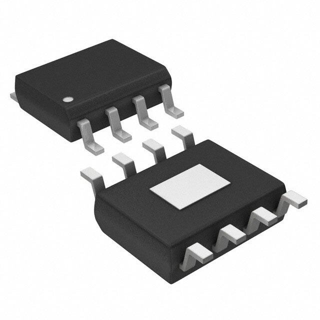
| 产品图片 |
|
| 产品型号 | LT1963ET#PBF |
| rohs | 无铅 / 符合限制有害物质指令(RoHS)规范要求 |
| 产品系列 | - |
| 产品培训模块 | http://www.digikey.cn/PTM/IndividualPTM.page?site=cn&lang=zhs&ptm=30565 |
| 供应商器件封装 | TO-220-5 |
| 包装 | 管件 |
| 安装类型 | 通孔 |
| 封装/外壳 | TO-220-5 成形引线 |
| 工作温度 | -40°C ~ 125°C |
| 标准包装 | 50 |
| 电压-跌落(典型值) | 0.34V @ 1.5A |
| 电压-输入 | 2.1 V ~ 20 V |
| 电压-输出 | 1.21 V ~ 20 V |
| 电流-输出 | 1.5A |
| 电流-限制(最小值) | 1.6A |
| 稳压器拓扑 | 正,可调式 |
| 稳压器数 | 1 |


- 商务部:美国ITC正式对集成电路等产品启动337调查
- 曝三星4nm工艺存在良率问题 高通将骁龙8 Gen1或转产台积电
- 太阳诱电将投资9.5亿元在常州建新厂生产MLCC 预计2023年完工
- 英特尔发布欧洲新工厂建设计划 深化IDM 2.0 战略
- 台积电先进制程称霸业界 有大客户加持明年业绩稳了
- 达到5530亿美元!SIA预计今年全球半导体销售额将创下新高
- 英特尔拟将自动驾驶子公司Mobileye上市 估值或超500亿美元
- 三星加码芯片和SET,合并消费电子和移动部门,撤换高东真等 CEO
- 三星电子宣布重大人事变动 还合并消费电子和移动部门
- 海关总署:前11个月进口集成电路产品价值2.52万亿元 增长14.8%


PDF Datasheet 数据手册内容提取
LT1963 Series 1.5A, Low Noise, Fast Transient Response LDO Regulators FEATURES DESCRIPTIOU ■ Optimized for Fast Transient Response The LT®1963 series are low dropout regulators optimized ■ Output Current: 1.5A for fast transient response. The devices are capable of ■ Dropout Voltage: 340mV supplying 1.5A of output current with a dropout voltage of ■ Low Noise: 40µVRMS (10Hz to 100kHz) 340mV. Operating quiescent current is 1mA, dropping to ■ 1mA Quiescent Current <1µA in shutdown. Quiescent current is well controlled; it ■ No Protection Diodes Needed does not rise in dropout as it does with many other ■ Controlled Quiescent Current in Dropout regulators. In addition to fast transient response, the ■ Fixed Output Voltages: 1.5V, 1.8V, 2.5V, 3.3V LT1963 regulators have very low output noise which ■ Adjustable Output from 1.21V to 20V makes them ideal for sensitive RF supply applications. ■ <1µA Quiescent Current in Shutdown Output voltage range is from 1.21V to 20V. The LT1963 ■ Stable with 10µF Output Capacitor regulators are stable with output capacitors as low as ■ Reverse Battery Protection 10µF. Internal protection circuitry includes reverse battery ■ No Reverse Current protection, current limiting, thermal limiting and reverse ■ Thermal Limiting current protection. The devices are available in fixed ■ 5-Lead TO-220, DD, 3-Lead SOT-223, 8-Lead SO output voltages of 1.5V, 1.8V, 2.5V, 3.3V and as an and 16-Lead TSSOP Packages adjustable device with a 1.21V reference voltage. The LT1963 regulators are available in 5-lead TO-220, DD, APPLICATIOU S 3-lead SOT-223, 8-lead SO, and Exposed Pad 16-lead TSSOP packages. ■ 3.3V to 2.5V Logic Power Supplies ■ Post Regulator for Switching Supplies , LTC and LT are registered trademarks of Linear Technology Corporation. All other trademarks are the property of their respective owners. Protected by U.S. Patents, including 6118263, 6144250. TYPICAL APPLICATIOUN Dropout Voltage 400 3.3V to 2.5V Regulator 350 V) 300 m + IN OUT + 21..55VA AGE ( 250 T L VIN > 3V 10µF LT1963-2.5 10µF VO 200 T U SHDN SENSE PO 150 O R GND D 100 1963 TA01 50 0 0 0.2 0.4 0.6 0.8 1.0 1.2 1.4 1.6 OUTPUT CURRENT (A) 1963 TA02 1963fc 1
LT1963 Series ABSOLUTE W AXIW UW RATIU GS (Note 1) IN Pin Voltage........................................................±20V SHDN Pin Voltage................................................. ±20V OUT Pin Voltage ....................................................±20V Output Short-Circuit Duration......................... Indefinite Input to Output Differential Voltage (Note 2) .........±20V Operating Junction Temperature Range –40°C to 125°C SENSE Pin Voltage ............................................... ±20V Storage Temperature Range................. –65°C to 150°C ADJ Pin Voltage...................................................... ±7V Lead Temperature (Soldering, 10 sec)..................300°C PACKAGE/ORDER IU FORW ATIOU TOP VIEW FRONT VIEW FRONT VIEW SENSE/ GND 1 16 GND 5 SENSE/ADJ* 5 ADJ* NC 2 15 NC 4 OUT 4 OUT OUT 3 14 IN TAGBN IDS 3 GND 3 GND OUT 4 13 IN *PIN 6= SENSE FOR LT1963-1.5/ 2 IN 2 IN OUT 5 17 12 IN LT1963-1.8/LT1963-2.5/ 1 SHDN 1 SHDN LT1963-3.3 SENSE/ADJ* 6 11 NC = ADJ FOR LT1963 Q PACKAGE TAB IS T PACKAGE 5-LEAD PLASTIC DD GND 5-LEAD PLASTIC TO-220 GND 7 10 SHDN GND 8 9 GND *PIN 5= SENSE FOR LT1963-1.5/LT1963-1.8/ *PIN 5= SENSE FOR LT1963-1.5/LT1963-1.8/ LT1963-2.5/LT1963-3.3 LT1963-2.5/LT1963-3.3 FE PACKAGE 16-LEAD PLASTIC TSSOP = ADJ FOR LT1963 = ADJ FOR LT1963 EXPOSED PAD (PIN 17) IS GND. MUST BE TJMAX = 150°C, θJA = 30°C/W TJMAX = 150°C, θJA = 50°C/W SOLDERED TO THE PCB. TJMAX = 150°C, θJA = 38°C/W ORDER PART NUMBER ORDER PART NUMBER ORDER PART NUMBER FE PART MARKING LT1963EQ LT1963ET LT1963EFE 1963EFE LT1963EQ-1.5 LT1963ET-1.5 LT1963EFE-1.5 1963EFE15 LT1963EQ-1.8 LT1963ET-1.8 LT1963EFE-1.8 1963EFE18 LT1963EQ-2.5 LT1963ET-2.5 LT1963EFE-2.5 1963EFE25 LT1963EQ-3.3 LT1963ET-3.3 LT1963EFE-3.3 1963EFE33 TOP VIEW FRONT VIEW OUT 1 8 IN 3 OUT SENSE/ADJ* 2 7 GND TAB IS GND 3 6 GND GND 2 GND NC 4 5 SHDN 1 IN S8 PACKAGE 8-LEAD PLASTIC SO ST PACKAGE *PIN 2= SENSE FOR LT1963-1.5/LT1963-1.8/ 3-LEAD PLASTIC SOT-223 LT1963-2.5/LT1963-3.3 TJMAX = 150°C, θJA = 50°C/W = ADJ FOR LT1963 TJMAX = 150°C, θJA = 70°C/W ORDER PART NUMBER ST PART MARKING ORDER PART NUMBER S8 PART MARKING LT1963EST-1.5 196315 LT1963ES8 1963 LT1963EST-1.8 196318 LT1963ES8-1.5 196315 LT1963EST-2.5 196325 LT1963ES8-1.8 196318 LT1963EST-3.3 196333 LT1963ES8-2.5 196325 LT1963ES8-3.3 196333 Order Options Tape and Reel: Add #TR Lead Free: Add #PBF Lead Free Tape and Reel: Add #TRPBF Lead Free Part Marking: http://www.linear.com/leadfree/ Consult LTC Marketing for parts specified with wider operating temperature ranges. 1963fc 2
LT1963 Series ELECTRICAL CHARACTERISTICS The ● denotes specifications which apply over the full operating temperature range, otherwise specifications are TA = 25°C. (Note 3) PARAMETER CONDITIONS MIN TYP MAX UNITS Minimum Input Voltage (Notes 4,12) I = 0.5A 1.9 V LOAD I = 1.5A 2.5V < V < 20V, 1mA < I < 1.5A ● 2.1 2.5 V LOAD IN LOAD Regulated Output Voltage (Note 5) LT1963-1.5 V = 2.21V, I = 1mA 1.477 1.500 1.523 V IN LOAD 2.5V < V < 20V, 1mA < I < 1.5A ● 1.447 1.500 1.545 V IN LOAD LT1963-1.8 V = 2.3V, I = 1mA 1.773 1.800 1.827 V IN LOAD 2.8V < V < 20V, 1mA < I < 1.5A ● 1.737 1.800 1.854 V IN LOAD LT1963-2.5 V = 3V, I = 1mA 2.462 2.500 2.538 V IN LOAD 3.5V < V < 20V, 1mA < I < 1.5A ● 2.412 2.500 2.575 V IN LOAD LT1963-3.3 V = 3.8V, I = 1mA 3.250 3.300 3.350 V IN LOAD 4.3V < V < 20V, 1mA < I < 1.5A ● 3.200 3.300 3.400 V IN LOAD ADJ Pin Voltage LT1963 V = 2.21V, I = 1mA 1.192 1.210 1.228 V IN LOAD (Notes 4, 5) 2.5V < V < 20V, 1mA < I < 1.5A ● 1.174 1.210 1.246 V IN LOAD Line Regulation LT1963-1.5 ∆VIN = 2.21V to 20V, ILOAD = 1mA ● 2.0 10 mV LT1963-1.8 ∆VIN = 2.3V to 20V, ILOAD = 1mA ● 2.5 10 mV LT1963-2.5 ∆VIN = 3V to 20V, ILOAD = 1mA ● 3.0 10 mV LT1963-3.3 ∆VIN = 3.8V to 20V, ILOAD = 1mA ● 3.5 10 mV LT1963 (Note 4) ∆VIN = 2.21V to 20V, ILOAD = 1mA ● 1.5 10 mV Load Regulation LT1963-1.5 VIN = 2.5V, ∆ILOAD = 1mA to 1.5A 2 9 mV VIN = 2.5V, ∆ILOAD = 1mA to 1.5A ● 18 mV LT1963-1.8 VIN = 2.8V, ∆ILOAD = 1mA to 1.5A 2 10 mV VIN = 2.8V, ∆ILOAD = 1mA to 1.5A ● 20 mV LT1963-2.5 VIN = 3.5V, ∆ILOAD = 1mA to 1.5A 2.5 15 mV VIN = 3.5V, ∆ILOAD = 1mA to 1.5A ● 30 mV LT1963-3.3 VIN = 4.3V, ∆ILOAD = 1mA to 1.5A 3 20 mV VIN = 4.3V, ∆ILOAD = 1mA to 1.5A ● 35 mV LT1963 (Note 4) VIN = 2.5V, ∆ILOAD = 1mA to 1.5A 2 8 mV VIN = 2.5V, ∆ILOAD = 1mA to 1.5A ● 15 mV Dropout Voltage I = 1mA 0.02 0.06 V LOAD V = V I = 1mA ● 0.10 V IN OUT(NOMINAL) LOAD (Notes 6, 7, 12) I = 100mA 0.10 0.17 V LOAD I = 100mA ● 0.22 V LOAD I = 500mA 0.19 0.27 V LOAD I = 500mA ● 0.35 V LOAD I = 1.5A 0.34 0.45 V LOAD I = 1.5A ● 0.55 V LOAD GND Pin Current I = 0mA ● 1.0 1.5 mA LOAD V = V + 1V I = 1mA ● 1.1 1.6 mA IN OUT(NOMINAL) LOAD (Notes 6, 8) ILOAD = 100mA ● 3.8 5.5 mA I = 500mA ● 15 25 mA LOAD I = 1.5A ● 80 120 mA LOAD Output Voltage Noise COUT = 10µF, ILOAD = 1.5A, BW = 10Hz to 100kHz 40 µVRMS ADJ Pin Bias Current (Notes 4, 9) 3 10 µA Shutdown Threshold V = Off to On ● 0.90 2 V OUT V = On to Off ● 0.25 0.75 V OUT SHDN Pin Current VSHDN = 0V 0.01 1 µA (Note 10) VSHDN = 20V 3 30 µA Quiescent Current in Shutdown VIN = 6V, VSHDN = 0V 0.01 1 µA Ripple Rejection V – V = 1.5V (Avg), V = 0.5V , 55 63 dB IN OUT RIPPLE P-P f = 120Hz, I = 0.75A RIPPLE LOAD 1963fc 3
LT1963 Series ELECTRICAL CHARACTERISTICS The ● denotes specifications which apply over the full operating temperature range, otherwise specifications are TA = 25°C. (Note 3) PARAMETER CONDITIONS MIN TYP MAX UNITS Current Limit V = 7V, V = 0V 2 A IN OUT VIN = VOUT(NOMINAL) + 1V, ∆VOUT = –0.1V ● 1.6 A Input Reverse Leakage Current (Note 13) Q, T, S8 Packages V = –20V, V = 0V ● 1 mA IN OUT ST Package V = –20V, V = 0V ● 2 mA IN OUT Reverse Output Current (Note 11) LT1963-1.5 VOUT = 1.5V, VIN < 1.5V 600 1200 µA LT1963-1.8 VOUT = 1.8V, VIN < 1.8V 600 1200 µA LT1963-2.5 VOUT = 2.5V, VIN < 2.5V 600 1200 µA LT1963-3.3 VOUT = 3.3V, VIN < 3.3V 600 1200 µA LT1963 (Note 4) VOUT = 1.21V, VIN < 1.21V 300 600 µA Note 1: Absolute Maximum Ratings are those values beyond which the life external resistor divider (two 4.12k resistors) for an output voltage of of a device may be impaired. 2.4V. The external resistor divider will add a 300µA DC load on the output. Note 2: Absolute maximum input to output differential voltage can not be Note 7: Dropout voltage is the minimum input to output voltage differential achieved with all combinations of rated IN pin and OUT pin voltages. With needed to maintain regulation at a specified output current. In dropout, the the IN pin at 20V, the OUT pin may not be pulled below 0V. The total output voltage will be equal to: V – V . IN DROPOUT measured voltage from IN to OUT can not exceed ±20V. Note 8: GND pin current is tested with V = V + 1V and a IN OUT(NOMINAL) Note 3: The LT1963 regulators are tested and specified under pulse load current source load. The GND pin current will decrease at higher input conditions such that TJ ≈ TA. The LT1963 is 100% tested at voltages. TA = 25°C. Performance at –40°C and 125°C is assured by design, Note 9: ADJ pin bias current flows into the ADJ pin. characterization and correlation with statistical process controls. Note 10: SHDN pin current flows into the SHDN pin. Note 4: The LT1963 (adjustable version) is tested and specified for these Note 11: Reverse output current is tested with the IN pin grounded and the conditions with the ADJ pin connected to the OUT pin. OUT pin forced to the rated output voltage. This current flows into the OUT Note 5: Operating conditions are limited by maximum junction pin and out the GND pin. temperature. The regulated output voltage specification will not apply for Note 12. For the LT1963, LT1963-1.5 and LT1963-1.8 dropout voltage will all possible combinations of input voltage and output current. When be limited by the minimum input voltage specification under some output operating at maximum input voltage, the output current range must be voltage/load conditions. limited. When operating at maximum output current, the input voltage Note 13. For the ST package, the input reverse leakage current increases range must be limited. due to the additional reverse leakage current for the SHDN pin, which is Note 6: To satisfy requirements for minimum input voltage, the LT1963 tied internally to the IN pin. (adjustable version) is tested and specified for these conditions with an 1963fc 4
LT1963 Series TYPICAL PERFORW AU CE CHARACTERISTICS Typical Dropout Voltage Guaranteed Dropout Voltage Dropout Voltage 500 600 500 TEST POINTS 450 V) 450 m 400 E (500 400 OLTAGE (mV) 332505000 TJ = 125°C POUT VOLTAG430000 TJ ≤ 125°C TJ ≤ 25°C OLTAGE (mV)332505000 IL = 1.5A V O V OPOUT 210500 TJ = 25°C EED DR200 OPOUT 210500 IL = 0.5A DR100 ARANT100 DR100 IL = 100mA 50 GU 50 IL = 1mA 0 0 0 0 0.2 0.4 0.6 0.8 1.0 1.2 1.4 1.6 0 0.2 0.4 0.6 0.8 1.0 1.2 1.4 1.6 –50 –25 0 25 50 75 100 125 OUTPUT CURRENT (A) 1963 • G01 OUTPUT CURRENT (A) 1963 • G02 TEMPERATURE (°C) 1963 G03 Quiescent Current LT1963-1.5 Output Voltage LT1963-1.8 Output Voltage 1.4 1.54 1.84 IL = 1mA IL = 1mA 1.2 LT1963-1.5/-1.8/-2.5/-3.3 1.53 1.83 UIESCENT CURRENT (mA) 1000....0864 LT1963 OUTPUT VOLTAGE (V)11111.....5554421098 OUTPUT VOLTAGE (V)11111.....8887721098 Q VIN = 6V 0.2 RL = ∞, IL = 0 1.47 1.77 VSHDN = VIN 0 1.46 1.76 –50 –25 0 25 50 75 100 125 –50 –25 0 25 50 75 100 125 –50 –25 0 25 50 75 100 125 TEMPERATURE (°C) 1963 G04 TEMPERATURE (°C) 1963 G04i TEMPERATURE (°C) 1963 G05 LT1963-2.5 Output Voltage LT1963-3.3 Output Voltage LT1963 ADJ Pin Voltage 2.58 3.38 1.230 IL = 1mA IL = 1mA IL = 1mA 2.56 3.36 1.225 2.54 3.34 1.220 V) V) V) GE (2.52 GE (3.32 GE (1.215 A A A T T T OL2.50 OL3.30 OL1.210 V V V T T N TPU2.48 TPU3.28 J PI1.205 U U D O2.46 O3.26 A1.200 2.44 3.24 1.195 2.42 3.22 1.190 –50 –25 0 25 50 75 100 125 –50 –25 0 25 50 75 100 125 –50 –25 0 25 50 75 100 125 TEMPERATURE (°C) TEMPERATURE (°C) TEMPERATURE (°C) 1963 G06 1963 G07 1963 G08 1963fc 5
LT1963 Series TYPICAL PERFORW AU CE CHARACTERISTICS LT1963-1.5 Quiescent Current LT1963-1.8 Quiescent Current LT1963-2.5 Quiescent Current 14 14 14 TJ = 25°C TJ = 25°C TJ = 25°C 12 RVSLH =D ∞N = VIN 12 RVSLH =D ∞N = VIN 12 RVSLH =D ∞N = VIN QUIESCENT CURRENT (mA) 10864 QUIESCENT CURRENT (mA) 10864 QUIESCENT CURRENT (mA) 10864 2 2 2 0 0 0 0 1 2 3 4 5 6 7 8 9 10 0 1 2 3 4 5 6 7 8 9 10 0 1 2 3 4 5 6 7 8 9 10 INPUT VOLTAGE (V) INPUT VOLTAGE (V) INPUT VOLTAGE (V) 1963 G08i 1963 G09 1963 G10 LT1963-3.3 Quiescent Current LT1963 Quiescent Current LT1963-1.5 GND Pin Current NT (mA) 111420 TRVJSL H ==D 2∞N5 =°C VIN NT (mA) 111...420 TRVJSL H ==D 24N5. 3=°Ck VIN T (mA) 2250 VT*FJS OH=RD 2N 5V =°OC UVTIN = 1.5V E E N 15 RR 8 RR 0.8 RE U U R C C U UIESCENT 64 UIESCENT 00..64 GND PIN C 10 RL = 5, IL = 300mA* Q Q 5 RL = 15, IL = 100mA* 2 0.2 RL = 150, IL = 10mA* 0 0 0 0 1 2 3 4 5 6 7 8 9 10 0 2 4 6 8 10 12 14 16 18 20 0 1 2 3 4 5 6 7 8 9 10 INPUT VOLTAGE (V) INPUT VOLTAGE (V) INPUT VOLTAGE (V) 1963 G11 1963 G12 LT1963 G12i LT1963-1.8 GND Pin Current LT1963-2.5 GND Pin Current LT1963-3.3 GND Pin Current 25 25 25 TJ = 25°C TJ = 25°C TJ = 25°C VSHDN = VIN VSHDN = VIN VSHDN = VIN 20 *FOR VOUT = 1.8V 20 *FOR VOUT = 2.5V 20 *FOR VOUT = 3.3V A) A) A) m m m NT ( 15 NT ( 15 NT ( 15 RE RE RL = 8.33, IL = 300mA* RE R R R U U U N C 10 N C 10 N C 10 RL = 11, IL = 300mA* D PI RL = 6, IL = 300mA* D PI D PI GN 5 RL = 18, IL = 100mA* GN 5 RL = 25, IL = 100mA* GN 5 RL = 33, IL = 100mA* RL = 180, IL = 10mA* RL = 250, IL = 10mA* RL = 330, IL = 100mA* 0 0 0 0 1 2 3 4 5 6 7 8 9 10 0 1 2 3 4 5 6 7 8 9 10 0 1 2 3 4 5 6 7 8 9 10 INPUT VOLTAGE (V) INPUT VOLTAGE (V) INPUT VOLTAGE (V) 1963 G13 1963 G14 1963 G15 1963fc 6
LT1963 Series TYPICAL PERFORW AU CE CHARACTERISTICS LT1963 GND Pin Current LT1963-1.5 GND Pin Current LT1963-1.8 GND Pin Current 10 100 100 TJ = 25°C TJ = 25°C TJ = 25°C VSHDN = VIN 90 VSHDN = VIN 90 VSHDN = VIN 8 *FOR VOUT = 1.21V 80 *FOR VOUT = 1.5V 80 *FOR VOUT = 1.8V mA) mA) 70 RL = 1, IL = 1.5A* mA) 70 RENT ( 6 RL = 4.33, IL = 300mA* RENT ( 60 RENT ( 60 RL = 1.2, IL = 1.5A* UR UR 50 UR 50 C C C PIN 4 PIN 40 RL = 1.5, IL = 1A* PIN 40 ND RL = 12.1, IL = 100mA* ND 30 ND 30 RL = 1.8, IL = 1A* G G G 2 20 RL = 3, IL = 500mA* 20 RL = 121, IL = 10mA* 10 10 RL = 3.6, IL = 500mA* 0 0 0 0 1 2 3 4 5 6 7 8 9 10 0 1 2 3 4 5 6 7 8 9 10 0 1 2 3 4 5 6 7 8 9 10 INPUT VOLTAGE (V) INPUT VOLTAGE (V) INPUT VOLTAGE (V) 1963 G16 1963 G16i 1963 G17 LT1963-2.5 GND Pin Current LT1963-3.3 GND Pin Current LT1963 GND Pin Current 100 100 100 TJ = 25°C TJ = 25°C TJ = 25°C 90 VSHDN = VIN 90 VSHDN = VIN 90 VSHDN = VIN 80 *FOR VOUT = 2.5V 80 *FOR VOUT = 3.3V 80 *FOR VOUT = 1.21V A) A) A) m 70 m 70 m 70 T ( RL = 1.67, IL = 1.5A* T ( RL = 2.2, IL = 1.5A* T ( N 60 N 60 N 60 E E E URR 50 URR 50 URR 50 RL = 0.81, IL = 1.5A* C C C N 40 N 40 N 40 GND PI 30 RL = 2.5, IL = 1A* GND PI 30 RL = 3.3, IL = 1A* GND PI 30 RL = 1.21, IL = 1A* 20 20 20 10 RL = 5, IL = 500mA* 10 RL = 6.6, IL = 500mA* 10 RL = 2.42, IL = 500mA* 0 0 0 0 1 2 3 4 5 6 7 8 9 10 0 1 2 3 4 5 6 7 8 9 10 0 1 2 3 4 5 6 7 8 9 10 INPUT VOLTAGE (V) INPUT VOLTAGE (V) INPUT VOLTAGE (V) 1963 G18 1963 G19 1963 G20 GND Pin Current vs I SHDN Pin Threshold (On-to-Off) SHDN Pin Threshold (Off-to-On) LOAD 100 1.0 1.0 VIN = VOUT (NOMINAL) +1V IL = 1mA 90 0.9 0.9 IL = 1.5A 80 0.8 0.8 mA) 70 D (V) 0.7 D (V) 0.7 NT ( 60 HOL 0.6 HOL 0.6 RE ES ES IL = 1mA UR 50 HR 0.5 HR 0.5 C T T N 40 N 0.4 N 0.4 PI PI PI ND 30 DN 0.3 DN 0.3 G H H 20 S 0.2 S 0.2 10 0.1 0.1 0 0 0 0 0.2 0.4 0.6 0.8 1.0 1.2 1.4 1.6 –50 –25 0 25 50 75 100 125 –50 –25 0 25 50 75 100 125 OUTPUT CURRENT (A) TEMPERATURE (°C) TEMPERATURE (°C) 1963 G21 1963 G22 1963 G23 1963fc 7
LT1963 Series TYPICAL PERFORW AU CE CHARACTERISTICS SHDN Pin Input Current SHDN Pin Input Current ADJ Pin Bias Current 5.0 7 5.0 VSHDN = 20V 4.5 4.5 6 A)µ 4.0 A)µ A) 4.0 NT ( 3.5 NT ( 5 T (µ 3.5 E E N RR 3.0 RR RE 3.0 U U 4 R C C U UT 2.5 UT S C 2.5 N INP 2.0 N INP 3 N BIA 2.0 HDN PI 11..50 HDN PI 2 ADJ PI 11..50 S S 1 0.5 0.5 0 0 0 0 2 4 6 8 10 12 14 16 18 20 –50 –25 0 25 50 75 100 125 –50 –25 0 25 50 75 100 125 SHDN PIN VOLTAGE (V) TEMPERATURE (°C) TEMPERATURE (°C) 1963 G24 1963 G25 1963 G26 Current Limit Current Limit Reverse Output Current 3.0 4.0 5.0 VIN = 7V TJ = 25°C 3.5 VOUT = 0V 4.5 VIN = 0V 2.5 A) m 4.0 LT1963-1.5 TJ = 25°C 3.0 T ( CURRENT LIMIT (A) 211...050 TJ = 125°C TJ = –50°C CURRENT LIMIT (A) 2211....5050 VERSE OUTPUT CURREN 332211......505050 LT19L6T31-916.38 LT19L6T31-926.53-3.3 0.5 0.5 RE ∆VOUT = 100mV 0.5 0 0 0 0 2 4 6 8 10 12 14 16 18 20 –50 –25 0 25 50 75 100 125 0 1 2 3 4 5 6 7 8 9 10 INPUT/OUTPUT DIFFERENTIAL (V) TEMPERATURE (°C) OUTPUT VOLTAGE (V) CURRENT FLOWS INTO OUTPUT PIN 1963 G27 1963 G28 VOUT = VADJ (LT1963) VOUT = VFB (LT1963-1.5/-1.8/-2.5/-3.3) 1963 G29 Reverse Output Current Ripple Rejection Ripple Rejection 1.0 80 76 VIN = 0V mA) 00..98 VVOOUUTT == 11..251VV ( L(LTT11996633-1).5) 70 74 RSE OUTPUT CURRENT ( 00000.....76543 VVVOOOUUUTTT === 123...853VVV (((LLLTTT111L999T66613339---61233...853-1))).5/L-1T.189/-623.5/-3.3 RIPPLE REJECTION (dB) 6543200000 COUT +=1 100 ×0Cµ 1OFµU TFTA C=NE 1TR0AAµLMFU IMTCANTALUM RIPPLE REJECTION (dB) 77662086 VE 0.2 RE 0.1 10 IL = 0.75A 64 IVLI N= =0 .V7O5UAT(NOMINAL) +1V + 0.5VP-P VIN = VOUT(NOMINAL) +1V + 50mVRMS RIPPLE RIPPLE AT f = 120Hz 0 0 62 –50 –25 0 25 50 75 100 125 10 100 1k 10k 100k 1M –50 –25 0 25 50 75 100 125 TEMPERATURE (°C) FREQUENCY (Hz) TEMPERATURE (°C) 1963 G30 1963 G31 1963 G32 1963fc 8
LT1963 Series TYPICAL PERFORW AU CE CHARACTERISTICS LT1963 Minimum Input Voltage Load Regulation Output Noise Spectral Density 3.0 10 1.0 Hz) COUT = 10µF NPUT VOLTAGE (V) 221...505 IL I=L 1=. 51A00mA IL = 500mA GULATION (mV) –505 LT1L9T6139-26.35-1.L5T196L3T-119.863 ECTRAL DENSITY (V/µ√ 0.1 ILLT =119.653A-3.3 LT1963-2.5 M I RE LT1963-3.3 SP MINIMU 10..05 LOAD ––1105 VI(NL T=1 V9O6U3T-(1N.5O/M-1IN.8A/L-)2 +.51/V-3 .3) UT NOISE LT1963-1.8 LT1963-1.5 LT1963 V∆IINL == 21.m7VA (TLOT 119.56A3) OUTP0.01 0 –20 10 100 1k 10k 100k –50 –25 0 25 50 75 100 125 –50 –25 0 25 50 75 100 125 FREQUENCY (Hz) TEMPERATURE (°C) TEMPERATURE (°C) 1963 G35 1963 G33 1963 G34 RMS Output Noise vs Load Current (10Hz to 100kHz) LT1963-3.3 10Hz to 100kHz Output Noise 50 COUT = 10µF 45 )S M 40 LT1963-3.3 R V GE (µ 35 LT1963-2.5 A 30 T E VOL 25 LT1963-1.8 100µVV/ODUIVT OIS 20 LT1963-1.5 N LT1963 T 15 U P T 10 U O 5 0 0.0001 0.001 0.01 0.1 1 10 COUT = 10µF 1ms/DIV 1963 G37 LOAD CURRENT (A) ILOAD = 1.5A 1063 G36 LT1963-3.3 Transient Response LT1963-3.3 Transient Response 200 150 VIN = 4.3V OUTPUT VOLTAGE DEVIATION (mV)11–505500000 CCIONU =T =3 .130µµF FT TAANNTTAALLUUMM OUTPUT VOLTAGE DEVIATION (mV)–1–1055000000 –100 –150 0.6 1.5 LOADURRENT (A) 00..42 LOAD URRENT (A)10..05 VCC+1IIONN0U ==T× = 431 .31µ3µ0VFF0 C µTEAFR NTATAMANLITCUAMLUM C 0 C 0 0 2 4 6 8 10 12 14 16 18 20 0 50 100150 200250 300350400 450500 TIME (µs) 1963 G38 TIME (µs) 1963 G39 1963fc 9
LT1963 Series PIU FUU CTIOU S OUT: Output. The output supplies power to the load. A ADJ: Adjust. For the adjustable LT1963, this is the input to minimum output capacitor of 10µF is required to prevent the error amplifier. This pin is internally clamped to ±7V. oscillations. Larger output capacitors will be It has a bias current of 3µA which flows into the pin. The required for applications with large transient loads to limit ADJ pin voltage is 1.21V referenced to ground and the peak voltage transients. See the Applications Information output voltage range is 1.21V to 20V. section for more information on output capacitance and SHDN: Shutdown. The SHDN pin is used to put the LT1963 reverse output characteristics. regulators into a low power shutdown state. The output SENSE: Sense. For fixed voltage versions of the LT1963 will be off when the SHDN pin is pulled low. The SHDN pin (LT1963-1.5/LT1963-1.8/LT1963-2.5/LT1963-3.3), the can be driven either by 5V logic or open-collector logic SENSE pin is the input to the error amplifier. Optimum with a pull-up resistor. The pull-up resistor is required to regulation will be obtained at the point where the SENSE supply the pull-up current of the open-collector gate, pin is connected to the OUT pin of the regulator. In critical normally several microamperes, and the SHDN pin cur- applications, small voltage drops are caused by the resis- rent, typically 3µA. If unused, the SHDN pin must be tance (R ) of PC traces between the regulator and the load. connected to V . The device will be in the low power P IN These may be eliminated by connecting the SENSE pin to shutdown state if the SHDN pin is not connected. the output at the load as shown in Figure 1 (Kelvin Sense IN: Input. Power is supplied to the device through the IN Connection). Note that the voltage drop across the exter- pin. A bypass capacitor is required on this pin if the device nal PC traces will add to the dropout voltage of the regu- is more than six inches away from the main input filter lator. The SENSE pin bias current is 600µA at the nominal capacitor. In general, the output impedance of a battery rated output voltage. The SENSE pin can be pulled below rises with frequency, so it is advisable to include a bypass ground (as in a dual supply system where the regulator capacitor in battery-powered circuits. A bypass capacitor load is returned to a negative supply) and still allow the in the range of 1µF to 10µF is sufficient. The LT1963 regu- device to start and operate. lators are designed to withstand reverse voltages on the IN pin with respect to ground and the OUT pin. In the case of IN OUT a reverse input, which can happen if a battery is plugged RP in backwards, the device will act as if there is a diode in LT1963 + + series with its input. There will be no reverse current flow SHDN SENSE VIN LOAD into the regulator and no reverse voltage will appear at the GND load. The device will protect both itself and the load. RP 1963 F01 Exposed Pad: GND. The Exposed Pad (FE Package) is ground and must be soldered to the PCB for rated thermal Figure 1. Kelvin Sense Connection performance. 1963fc 10
LT1963 Series APPLICATIOU S IU FORW ATIOU The LT1963 series are 1.5A low dropout regulators opti- The adjustable device is tested and specified with the ADJ mized for fast transient response. The devices are capable pin tied to the OUT pin for an output voltage of 1.21V. of supplying 1.5A at a dropout voltage of 350mV. The low Specifications for output voltages greater than 1.21V will operating quiescent current (1mA) drops to less than 1µA be proportional to the ratio of the desired output voltage to in shutdown. In addition to the low quiescent current, the 1.21V: V /1.21V. For example, load regulation for an OUT LT1963 regulators incorporate several protection features output current change of 1mA to 1.5A is –3mV typical at which make them ideal for use in battery-powered sys- V = 1.21V. At V = 5V, load regulation is: OUT OUT tems. The devices are protected against both reverse input (5V/1.21V)(–3mV) = –12.4mV and reverse output voltages. In battery backup applica- tions where the output can be held up by a backup battery Output Capacitance and Transient Response when the input is pulled to ground, the LT1963-X acts like The LT1963 regulators are designed to be stable with a wide it has a diode in series with its output and prevents reverse range of output capacitors. The ESR of the output capacitor current flow. Additionally, in dual supply applications affects stability, most notably with small capacitors. A mini- where the regulator load is returned to a negative supply, mum output capacitor of 10µF with an ESR in the range of the output can be pulled below ground by as much as 20V 50mΩ to 3Ω is recommended to prevent oscillations. Larger and still allow the device to start and operate. values of output capacitance can decrease the peak devia- tions and provide improved transient response for larger Adjustable Operation load current changes. Bypass capacitors, used to decouple The adjustable version of the LT1963 has an output individual components powered by the LT1963, will in- voltage range of 1.21V to 20V. The output voltage is set by crease the effective output capacitor value. the ratio of two external resistors as shown in Figure 2. The Extra consideration must be given to the use of ceramic device servos the output to maintain the voltage at the ADJ capacitors. Ceramic capacitors are manufactured with a pin at 1.21V referenced to ground. The current in R1 is variety of dielectrics, each with different behavior across then equal to 1.21V/R1 and the current in R2 is the current temperature and applied voltage. The most common di- in R1 plus the ADJ pin bias current. The ADJ pin bias electrics used are specified with EIA temperature charac- current, 3µA at 25°C, flows through R2 into the ADJ pin. teristic codes of Z5U, Y5V, X5R and X7R. The Z5U and Y5V The output voltage can be calculated using the formula in dielectrics are good for providing high capacitances in a Figure 2. The value of R1 should be less than 4.17k to small package, but they tend to have strong voltage and minimize errors in the output voltage caused by the ADJ temperature coefficients as shown in Figures 2 and 3. pin bias current. Note that in shutdown the output is turned When used with a 5V regulator, a 16V 10µF Y5V capacitor off and the divider current will be zero. can exhibit an effective value as low as 1µF to 2µF for the DC bias voltage applied and over the operating tempera- IN OUT VOUT ture range. The X5R and X7R dielectrics result in more + VIN LT1963 R2 stable characteristics and are more suitable for use as the ADJ output capacitor. The X7R type has better stability across GND R1 temperature, while the X5R is less expensive and is available in higher values. Care still must be exercised 1963 F02 when using X5R and X7R capacitors; the X5R and X7R VOUT=1.21V⎛⎜1+R2⎞⎟+(IADJ)(R2) codes only specify operating temperature range and maxi- ⎝ R1⎠ mum capacitance change over temperature. Capacitance VADJ=1.21V change due to DC bias with X5R and X7R capacitors is IADJ=3µA AT 25°C better than Y5V and Z5U capacitors, but can still be OUTPUT RANGE = 1.21V TO 20V significant enough to drop capacitor values below appro- Figure 2. Adjustable Operation priate levels. Capacitor DC bias characteristics tend to 1963fc 11
LT1963 Series APPLICATIOU S IU FORW ATIOU 20 operating region for all values of input-to-output voltage. BOTH CAPACITORS ARE 16V, 1210 CASE SIZE, 10µF The protection is designed to provide some output current 0 at all values of input-to-output voltage up to the device %) X5R E (–20 breakdown. U L A V When power is first turned on, as the input voltage rises, N –40 E I the output follows the input, allowing the regulator to start G N HA–60 up into very heavy loads. During the start-up, as the input C Y5V voltage is rising, the input-to-output voltage differential is –80 small, allowing the regulator to supply large output –100 currents. With a high input voltage, a problem can occur 0 2 4 6 8 10 12 14 16 DC BIAS VOLTAGE (V) wherein removal of an output short will not allow the 1963 F03 output voltage to recover. Other regulators, such as the LT1085, also exhibit this phenomenon, so it is not unique Figure 3. Ceramic Capacitor DC Bias Characteristics to the LT1963-X. 40 The problem occurs with a heavy output load when the 20 input voltage is high and the output voltage is low. Com- mon situations are immediately after the removal of a %) 0 X5R E ( short-circuit or when the shutdown pin is pulled high after U AL –20 the input voltage has already been turned on. The load line V N GE I –40 Y5V for such a load may intersect the output current curve at AN two points. If this happens, there are two stable output H –60 C operating points for the regulator. With this double inter- –80 BOTH CAPACITORS ARE 16V, section, the input power supply may need to be cycled down 1210 CASE SIZE, 10µF –100 to zero and brought up again to make the output recover. –50 –25 0 25 50 75 100 125 TEMPERATURE (°C) Output Voltage Noise 1963 F04 Figure 4. Ceramic Capacitor Temperature Characteristics The LT1963 regulators have been designed to provide low output voltage noise over the 10Hz to 100kHz bandwidth improve as component case size increases, but expected while operating at full load. Output voltage noise is typi- capacitance at operating voltage should be verified. cally 40nV/√Hz over this frequency bandwidth for the Voltage and temperature coefficients are not the only LT1963 (adjustable version). For higher output voltages sources of problems. Some ceramic capacitors have a (generated by using a resistor divider), the output voltage piezoelectric response. A piezoelectric device generates noise will be gained up accordingly. This results in RMS voltage across its terminals due to mechanical stress, noise over the 10Hz to 100kHz bandwidth of 14µV for RMS similar to the way a piezoelectric accelerometer or micro- the LT1963 increasing to 38µV for the LT1963-3.3. RMS phone works. For a ceramic capacitor the stress can be Higher values of output voltage noise may be measured induced by vibrations in the system or thermal transients. when care is not exercised with regards to circuit layout and testing. Crosstalk from nearby traces can induce Overload Recovery unwanted noise onto the output of the LT1963-X. Power Like many IC power regulators, the LT1963-X has safe supply ripple rejection must also be considered; the LT1963 operating area protection. The safe area protection de- regulators do not have unlimited power supply rejection creases the current limit as input-to-output voltage in- and will pass a small portion of the input noise through to creases and keeps the power transistor inside a safe the output. 1963fc 12
LT1963 Series APPLICATIOU S IU FORW ATIOU Thermal Considerations Table 2. SO-8 Package, 8-Lead SO COPPER AREA THERMAL RESISTANCE The power handling capability of the device is limited by the TOPSIDE* BACKSIDE BOARD AREA (JUNCTION-TO-AMBIENT) maximum rated junction temperature (125°C). The power 2500mm2 2500mm2 2500mm2 55°C/W dissipated by the device is made up of two components: 1000mm2 2500mm2 2500mm2 55°C/W 1. Output current multiplied by the input/output voltage 225mm2 2500mm2 2500mm2 63°C/W differential: (IOUT)(VIN – VOUT), and 100mm2 2500mm2 2500mm2 69°C/W * Device is mounted on topside 2. GND pin current multiplied by the input voltage: (I )(V ). Table 3. SOT-223 Package, 3-Lead SOT-223 GND IN The GND pin current can be found using the GND Pin COPPER AREA THERMAL RESISTANCE TOPSIDE* BACKSIDE BOARD AREA (JUNCTION-TO-AMBIENT) Current curves in the Typical Performance Characteris- 2500mm2 2500mm2 2500mm2 42°C/W tics. Power dissipation will be equal to the sum of the two components listed above. 1000mm2 2500mm2 2500mm2 42°C/W 225mm2 2500mm2 2500mm2 50°C/W The LT1963 series regulators have internal thermal lim- 100mm2 2500mm2 2500mm2 56°C/W iting designed to protect the device during overload 1000mm2 1000mm2 1000mm2 49°C/W conditions. For continuous normal conditions, the maxi- 1000mm2 0mm2 1000mm2 52°C/W mum junction temperature rating of 125°C must not be * Device is mounted on topside exceeded. It is important to give careful consideration to Table 4. FE Package, 16-Lead TSSOP all sources of thermal resistance from junction to ambi- ent. Additional heat sources mounted nearby must also COPPER AREA THERMAL RESISTANCE be considered. TOPSIDE* BACKSIDE BOARD AREA (JUNCTION-TO-AMBIENT) 2500mm2 2500mm2 2500mm2 38°C/W For surface mount devices, heat sinking is accomplished 1000mm2 2500mm2 2500mm2 43°C/W by using the heat spreading capabilities of the PC board 225mm2 2500mm2 2500mm2 48°C/W and its copper traces. Copper board stiffeners and plated 100mm2 2500mm2 2500mm2 60°C/W through-holes can also be used to spread the heat gener- * Device is mounted on topside ated by power devices. T Package, 5-Lead TO-220 The following tables list thermal resistance for several Thermal Resistance (Junction-to-Case) = 4°C/W different board sizes and copper areas. All measurements Calculating Junction Temperature were taken in still air on 1/16" FR-4 board with one ounce copper. Example: Given an output voltage of 3.3V, an input voltage range of 4V to 6V, an output current range of 0mA to Table 1. Q Package, 5-Lead DD COPPER AREA THERMAL RESISTANCE 500mA and a maximum ambient temperature of 50°C, TOPSIDE* BACKSIDE BOARD AREA (JUNCTION-TO-AMBIENT) what will the maximum junction temperature be? 2500mm2 2500mm2 2500mm2 23°C/W The power dissipated by the device will be equal to: 1000mm2 2500mm2 2500mm2 25°C/W I (V – V ) + I (V ) OUT(MAX) IN(MAX) OUT GND IN(MAX) 125mm2 2500mm2 2500mm2 33°C/W * Device is mounted on topside where, I = 500mA OUT(MAX) V = 6V IN(MAX) I at (I = 500mA, V = 6V) = 10mA GND OUT IN So, P = 500mA(6V – 3.3V) + 10mA(6V) = 1.41W 1963fc 13
LT1963 Series APPLICATIOU S IU FORW ATIOU Using a DD package, the thermal resistance will be in the device. If the input is left open circuit or grounded, the ADJ range of 23°C/W to 33°C/W depending on the copper pin will act like an open circuit when pulled below ground area. So the junction temperature rise above ambient will and like a large resistor (typically 5k) in series with a diode be approximately equal to: when pulled above ground. 1.41W(28°C/W) = 39.5°C In situations where the ADJ pin is connected to a resistor divider that would pull the ADJ pin above its 7V clamp The maximum junction temperature will then be equal to voltage if the output is pulled high, the ADJ pin input the maximum junction temperature rise above ambient current must be limited to less than 5mA. For example, a plus the maximum ambient temperature or: resistor divider is used to provide a regulated 1.5V output TJMAX = 50°C + 39.5°C = 89.5°C from the 1.21V reference when the output is forced to 20V. The top resistor of the resistor divider must be chosen to Protection Features limit the current into the ADJ pin to less than 5mA when the The LT1963 regulators incorporate several protection ADJ pin is at 7V. The 13V difference between OUT and ADJ features which make them ideal for use in battery-powered pins divided by the 5mA maximum current into the ADJ pin circuits. In addition to the normal protection features yields a minimum top resistor value of 2.6k. associated with monolithic regulators, such as current In circuits where a backup battery is required, several limiting and thermal limiting, the devices are protected different input/output conditions can occur. The output against reverse input voltages, reverse output voltages voltage may be held up while the input is either pulled to and reverse voltages from output to input. ground, pulled to some intermediate voltage, or is left Current limit protection and thermal overload protection open circuit. Current flow back into the output will follow are intended to protect the device against current overload the curve shown in Figure 5. conditions at the output of the device. For normal opera- When the IN pin of the LT1963 is forced below the OUT pin tion, the junction temperature should not exceed 125°C. or the OUT pin is pulled above the IN pin, input current will The input of the device will withstand reverse voltages of typically drop to less than 2µA. This can happen if the 20V. Current flow into the device will be limited to less than input of the device is connected to a discharged (low 1mA (typically less than 100µA) and no negative voltage voltage) battery and the output is held up by either a will appear at the output. The device will protect both itself backup battery or a second regulator circuit. The state of and the load. This provides protection against batteries the SHDN pin will have no effect on the reverse output that can be plugged in backward. current when the output is pulled above the input. The output of the LT1963 can be pulled below ground 5.0 without damaging the device. If the input is left open circuit LT1963 4.5 VOUT = VADJ or grounded, the output can be pulled below ground by A) m 4.0 LT1963-1.5 20V. For fixed voltage versions, the output will act like a NT ( 3.5 VOUT = VFB large resistor, typically 5k or higher, limiting current flow RE LT1963-1.8 to typically less than 600µA. For adjustable versions, the UT CUR 32..05 LTV1O9U6T3 =- 2V.5FB output will act like an open circuit; no current will flow out UTP 2.0 VOUT = VFB LT1963-3.3 of the pin. If the input is powered by a voltage source, the SE O 1.5 VOUT = VFB R output will source the short-circuit current of the device VE 1.0 TJ = 25°C and will protect itself by thermal limiting. In this case, RE 0.5 VCIUNR =R 0EVNT FLOWS INTO OUTPUT PIN grounding the SHDN pin will turn off the device and stop 0 0 1 2 3 4 5 6 7 8 9 10 the output from sourcing the short-circuit current. OUTPUT VOLTAGE (V) The ADJ pin of the adjustable device can be pulled above 1963 F05 or below ground by as much as 7V without damaging the Figure 5. Reverse Output Current 1963fc 14
LT1963 Series TYPICAL APPLICATIOU S SCR Pre-Regulator Provides Efficiency Over Line Variations L1 500µH LT1963-3.3 IN OUT 3.3VOUT L2 1N4148 + + 1.5A 10VAC AT 10000µF SHDN FB 22µF 115VIN GND 90-140 1k VAC 34k* 10VAC AT 115VIN 1N4002 1N4002 12.1k* +V “SYNC” 1N4002 2.4k TO ALL “+V” + C1A 200k POINTS + 1N4148 1/2 22µF 750Ω LT1018 – 0.1µF +V C1B 0.033µF 750Ω + +V 1/2 A1 + LT1018 1N4148 – LT1006 10k 10k – +V 10k 1µF +V L1 = COILTRONICS CTX500-2-52 LT1004 L2 = STANCOR P-8559 1.2V * = 1% FILM RESISTOR = NTE5437 1963 TA03 Paralleling of Regulators for Higher Output Current R1 0.01Ω LT1963-3.3 3.3V + IN OUT + 3A VIN > 3.7V C1010µF C222µF SHDN FB GND R2 0.01Ω LT1963 IN OUT R6 6.65k SHDN SHDN FB GND R7 4.12k R3 R4 R5 2.2k 2.2k 1k 3 + 8 1/2 1 LT1366 2 – 4 C3 0.01µF 1963 TA05 1963fc 15
LT1963 Series PACKAGE DESCRIPTIOU Q Package 5-Lead Plastic DD Pak (Reference LTC DWG # 05-08-1461) .060 (1.524) .390 – .415 .256 .060 TYP (9.906 – 10.541) .165 – .180 (6.502) (1.524) (4.191 – 4.572) .045 – .055 (1.143 – 1.397) 15° TYP +.008 .004 .060 .183 .330 – .370 .059 –.004 (1.524) (4.648) (1.499) ( +0.203) (8.382 – 9.398) 0.102 TYP –0.102 .095 – .115 (2.413 – 2.921) .075 (1.905) (7.3.60200) .143+–..001220 (1.B0.7S60C72) (0..303103 –– 0.0.52834) (1..207500 ±± 0.0.31025) ( +0.305) .028 – .038 BOTTOM VIEW OF DD PAK 3.632–0.508 (0.711 – 0.965) Q(DD5) 0502 HATCHED AREA IS SOLDER PLATED TYP COPPER HEAT SINK .420 .080 .420 .276 .350 .325 .205 .565 .565 .320 .090 .090 .067 .042 .067 .042 RECOMMENDED SOLDER PAD LAYOUT RECOMMENDED SOLDER PAD LAYOUT FOR THICKER SOLDER PASTE APPLICATIONS NOTE: 1. DIMENSIONS IN INCH/(MILLIMETER) 2. DRAWING NOT TO SCALE 1963fc 16
LT1963 Series PACKAGE DESCRIPTIOU S8 Package 8-Lead Plastic Small Outline (Narrow .150 Inch) (Reference LTC DWG # 05-08-1610) .189 – .197 .045 ±.005 (4.801 – 5.004) .050 BSC NOTE 3 8 7 6 5 .245 MIN .160 ±.005 .150 – .157 .228 – .244 (3.810 – 3.988) (5.791 – 6.197) NOTE 3 .030 ±.005 TYP 1 2 3 4 RECOMMENDED SOLDER PAD LAYOUT .010 – .020 × 45°(cid:31) .053 – .069 (0.254 – 0.508) (1.346 – 1.752) .004 – .010 .008 – .010 (0.203 – 0.254) 0°– 8° TYP (0.101 – 0.254) .016 – .050 .014 – .019 .050 (0.406 – 1.270) (0.355 – 0.483) (1.270) NOTE: INCHES TYP BSC 1. DIMENSIONS IN (MILLIMETERS) 2. DRAWING NOT TO SCALE 3. THESE DIMENSIONS DO NOT INCLUDE MOLD FLASH OR PROTRUSIONS. MOLD FLASH OR PROTRUSIONS SHALL NOT EXCEED .006" (0.15mm) SO8 0303 1963fc 17
LT1963 Series PACKAGE DESCRIPTIOU ST Package 3-Lead Plastic SOT-223 (Reference LTC DWG # 05-08-1630) .248 – .264 .129 MAX (6.30 – 6.71) .114 – .124 .059 MAX (2.90 – 3.15) .264 – .287 .248 BSC (6.70 – 7.30) .130 – .146 (3.30 – 3.71) .039 MAX .059 MAX .090 BSC .181 MAX .0905 .033 – .041 RECOMMENDED SOLDER PAD LAYOUT (2.30) (0.84 – 1.04) BSC 10° – 16° .010 – .014 .071 10° (0.25 – 0.36) (1.80) MAX MAX 10° – 16° .024 – .033 .012 .0008 – .0040 (0.60 – 0.84) (0.31) (0.0203 – 0.1016) .181 MIN (4.60) ST3 (SOT-233) 0502 BSC T Package 5-Lead Plastic TO-220 (Standard) (Reference LTC DWG # 05-08-1421) 0.147 – 0.155 0.165 – 0.180 0.390 – 0.415 (3.734 – 3.937) (4.191 – 4.572) 0.045 – 0.055 (9.906 – 10.541) DIA (1.143 – 1.397) 0.230 – 0.270 (5.842 – 6.858) 0.570 – 0.620 0.620 0.460 – 0.500 (14.478 – 15.748) (15.75) (11.684 – 12.700) 0.330 – 0.370 TYP 0.700 – 0.728 (8.382 – 9.398) (17.78 – 18.491) 0.095 – 0.115 SEATING PLANE (2.413 – 2.921) 0.152 – 0.202 0.260 – 0.320 (3.861 – 5.131) 0.155 – 0.195* (3.937 – 4.953) (6.60 – 8.13) 0.013 – 0.023 (0.330 – 0.584) 0.067 BSC 0.028 – 0.038 0.135 – 0.165 * MEASURED AT THE (1.70) (0.711 – 0.965) (3.429 – 4.191) SEATING PLANE T5 (TO-220) 0399 1963fc 18
LT1963 Series PACKAGE DESCRIPTIOU FE Package 16-Lead Plastic TSSOP (4.4mm) (Reference LTC DWG # 05-08-1663) Exposed Pad Variation BB 4.90 – 5.10* 3.58 (.193 – .201) (.141) 3.58 (.141) 16 151413121110 9 6.60 ±0.10 2.94 4.50 ±0.10 (.116) SEE NOTE 4 2.94 6.40 (.116) (.252) 0.45 ±0.05 BSC 1.05 ±0.10 0.65 BSC RECOMMENDED SOLDER PAD LAYOUT 1 2 3 4 5 6 7 8 1.10 4.30 – 4.50* (.0433) (.169 – .177) 0.25 MAX REF 0° – 8° 0.65 0.09 – 0.20 0.50 – 0.75 (.0256) 0.05 – 0.15 (.0035 – .0079) (.020 – .030) BSC (.002 – .006) 0.195 – 0.30 (.0077 – .0118) FE16 (BB) TSSOP 0204 TYP NOTE: 1. CONTROLLING DIMENSION: MILLIMETERS 4. RECOMMENDED MINIMUM PCB METAL SIZE MILLIMETERS FOR EXPOSED PAD ATTACHMENT 2. DIMENSIONS ARE IN (INCHES) *DIMENSIONS DO NOT INCLUDE MOLD FLASH. MOLD FLASH 3. DRAWING NOT TO SCALE SHALL NOT EXCEED 0.150mm (.006") PER SIDE 1963fc Information furnished by Linear Technology Corporation is believed to be accurate and reliable. 19 However, no responsibility is assumed for its use. Linear Technology Corporation makes no represen- tation that the interconnection of its circuits as described herein will not infringe on existing patent rights.
LT1963 Series TYPICAL APPLICATIOU S Adjustable Current Source R5 0.01Ω LT1963-1.8 IN OUT LOAD + R1 VIN > 2.7V 10Cµ1F 1k SHDN FB LT1004-1.2 GND R2 R4 R6 C3 R8 80.6k 2.2k 2.2k 1µF 100k R3 2k R7 2 + 8 470Ω 1/2 1 LT1366 3 – C2 4 NOTE: ADJUST R1 FOR 3.3µF 0A TO 1.5A CONSTANT CURRENT 1963 TA04 RELATED PARTS PART NUMBER DESCRIPTION COMMENTS LT1129 700mA, Micropower, LDO VIN: 4.2V to 30V, VOUT(MIN) = 3.75V, VDO = 0.40V, IQ = 50µA, ISD = 16µA, DD, SOT-223, S8, TO220, TSSOP20 Packages LT1175 500mA, Micropower Negative LDO VIN: –20V to –4.3V, VOUT(MIN) = –3.8V, VDO = 0.50V, IQ = 45µA, ISD = 10µA, DD, SOT-223, S8 Packages LT1185 3A, Negative LDO VIN: –35V to –4.2V, VOUT(MIN) = –2.40V, VDO = 0.80V, IQ = 2.5mA, ISD <1µA, TO220-5 Package LT1761 100mA, Low Noise Micropower, LDO VIN: 1.8V to 20V, VOUT(MIN) = 1.22V, VDO = 0.30V, IQ = 20µA, ISD <1µA, ThinSOT Package LT1762 150mA, Low Noise Micropower, LDO VIN: 1.8V to 20V, VOUT(MIN) = 1.22V, VDO = 0.30V, IQ = 25µA, ISD <1µA, MS8 Package LT1763 500mA, Low Noise Micropower, LDO VIN: 1.8V to 20V, VOUT(MIN) = 1.22V, VDO = 0.30V, IQ = 30µA, ISD <1µA, S8 Package LT1764/ 3A, Low Noise, Fast Transient Response, VIN: 2.7V to 20V, VOUT(MIN) = 1.21V, VDO = 0.34V, IQ = 1mA, ISD <1µA, LT1764A LDO DD, TO220 Packages LTC1844 150mA, Very Low Drop-Out LDO VIN: 6.5V to 1.6V, VOUT(MIN) = 1.25V, VDO = 0.08V, IQ = 40µA, ISD <1µA, ThinSOT Package LT1962 300mA, Low Noise Micropower, LDO VIN: 1.8V to 20V, VOUT(MIN) = 1.22V, VDO = 0.27V, IQ = 30µA, ISD <1µA, MS8 Package LT1963/ 1.5A, Low Noise, Fast Transient Response, VIN: 2.1V to 20V, VOUT(MIN) = 1.21V, VDO = 0.34V, IQ = 1mA, ISD <1µA, LT1963A LDO DD, TO220, SOT Packages LT1964 200mA, Low Noise Micropower, Negative VIN: –0.9V to –20V, VOUT(MIN) = –1.21V, VDO = 0.34V, IQ = 30µA, ISD = 3µA, LDO ThinSOT Package LT3020 100mA, Low Voltage VLDO VIN: 0.9V to 10V, VOUT(MIN) = 0.20, VDO = 0.15V, IQ = 120µA, ISD <3µA, DFN, MS8 Packages LT3023 Dual, 2x 100mA, Low Noise Micropower, VIN: 1.8V to 20V, VOUT(MIN) = 1.22V, VDO = 0.30V, IQ = 40µA, ISD <1µA, LDO DFN, MS10 Packages LT3024 Dual, 100mA/500mA, Low Noise Micropower, VIN: 1.8V to 20V, VOUT(MIN) = 1.22V, VDO = 0.30V, IQ = 60µA, ISD <1µA, LDO DFN, TSSOP Package LT3150 Fast Transient Response, Low Input Voltage VIN: –1.4V to 10V, VOUT(MIN) = 1.23V, VDO = 0.13V, IQ = 12mA, ISD = 25µA, GN16 Package 1963fc 20 Linear Technology Corporation LT 1105 • PRINTED IN USA 1630 McCarthy Blvd., Milpitas, CA 95035-7417 (408) 432-1900 ● FAX: (408) 434-0507 ● www.linear.com © LINEAR TECHNOLOGY CORPORATION 2005