ICGOO在线商城 > 集成电路(IC) > PMIC - 稳压器 - 线性 > LT3014HVES5#TRMPBF

 Datasheet下载
- 型号: LT3014HVES5#TRMPBF
- 制造商: LINEAR TECHNOLOGY
- 库位|库存: xxxx|xxxx
- 要求:
| 数量阶梯 | 香港交货 | 国内含税 |
| +xxxx | $xxxx | ¥xxxx |
查看当月历史价格
查看今年历史价格
LT3014HVES5#TRMPBF产品简介:
ICGOO电子元器件商城为您提供LT3014HVES5#TRMPBF由LINEAR TECHNOLOGY设计生产,在icgoo商城现货销售,并且可以通过原厂、代理商等渠道进行代购。 LT3014HVES5#TRMPBF价格参考。LINEAR TECHNOLOGYLT3014HVES5#TRMPBF封装/规格:PMIC - 稳压器 - 线性, Linear Voltage Regulator IC Positive Adjustable 1 Output 1.22 V ~ 60 V 20mA TSOT-23-5。您可以下载LT3014HVES5#TRMPBF参考资料、Datasheet数据手册功能说明书,资料中有LT3014HVES5#TRMPBF 详细功能的应用电路图电压和使用方法及教程。
LT3014HVES5#TRMPBF 是 Linear Technology(现为 Analog Devices)生产的一款 PMIC(电源管理集成电路),属于线性稳压器类别。该型号的线性稳压器具有高精度、低噪声和高输出电流的特点,适用于多种需要稳定电源的应用场景。以下是其主要应用场景:

 1. 精密仪器
   - LT3014 提供高精度的电压调节能力,适合用于要求高稳定性和低噪声的精密仪器,例如医疗设备、测试测量仪器和数据采集系统。
   - 其低输出噪声特性非常适合对信号质量要求极高的应用,如传感器接口和模拟信号处理电路。

 2. 通信设备
   - 在无线通信模块、基站和其他通信设备中,LT3014 可以为射频(RF)电路和数字信号处理器(DSP)提供稳定的电源。
   - 高效率和低功耗的设计使其能够在高温环境下保持可靠运行。

 3. 工业自动化
   - 工业控制系统和自动化设备需要可靠的电源供应,LT3014 的高输出电流能力和宽输入电压范围使其成为理想选择。
   - 它可以为微控制器、FPGA 和其他核心组件提供稳定的电源支持。

 4. 汽车电子
   - 虽然 LT3014 并非专为汽车级设计,但其高性能特点使其在某些非关键汽车应用中仍然适用,例如信息娱乐系统、导航模块和传感器供电。
   - 它能够承受较高的环境温度(扩展温度范围版本支持高达 125°C 的工作温度),适应汽车内部的严苛条件。

 5. 便携式设备
   - 对于电池供电的便携式设备(如手持终端、便携式医疗设备等),LT3014 的高效能和小封装尺寸有助于节省空间并延长电池寿命。
   - 其快速瞬态响应能力确保设备在负载变化时仍能保持稳定运行。

 6. 嵌入式系统
   - 在嵌入式计算平台中,LT3014 可为处理器、存储器和其他外设提供精确的电源支持。
   - 其可调输出电压范围(0.8V 至 20V)和高达 2A 的输出电流能力,满足了多种嵌入式系统的电源需求。

 总结
LT3014HVES5#TRMPBF 的高性能特点使其广泛应用于需要高精度、低噪声和高稳定性的场景。无论是工业、通信还是消费类电子产品,这款线性稳压器都能提供可靠的电源解决方案,同时支持紧凑型设计以适应现代电子设备的空间限制。
| 参数 | 数值 |
| 产品目录 | 集成电路 (IC) |
| 描述 | IC REG LDO ADJ 20MA TSOT23-5 |
| 产品分类 | |
| 品牌 | Linear Technology |
| 数据手册 | http://www.linear.com/docs/7318 |
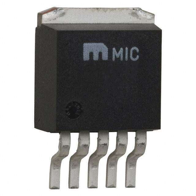
| 产品图片 |
|
| 产品型号 | LT3014HVES5#TRMPBF |
| rohs | 无铅 / 符合限制有害物质指令(RoHS)规范要求 |
| 产品系列 | - |
| 产品培训模块 | http://www.digikey.cn/PTM/IndividualPTM.page?site=cn&lang=zhs&ptm=30565 |
| 供应商器件封装 | TSOT-23-5 |
| 其它名称 | LT3014HVES5#TRMPBFCT |
| 包装 | 剪切带 (CT) |
| 安装类型 | 表面贴装 |
| 封装/外壳 | SOT-23-5 细型,TSOT-23-5 |
| 工作温度 | -40°C ~ 125°C |
| 标准包装 | 1 |
| 电压-跌落(典型值) | 0.35V @ 20mA |
| 电压-输入 | 3 V ~ 80 V |
| 电压-输出 | 1.22 V ~ 60 V |
| 电流-输出 | 20mA |
| 电流-限制(最小值) | 25mA |
| 稳压器拓扑 | 正,可调式 |
| 稳压器数 | 1 |


PDF Datasheet 数据手册内容提取
LT3014 20mA, 3V to 80V Low Dropout Micropower Linear Regulator FEATURES DESCRIPTION n Wide Input Voltage Range: 3V to 80V The LT®3014 is a high voltage, micropower low dropout n Low Quiescent Current: 7µA linear regulator. The device is capable of supplying 20mA of n Low Dropout Voltage: 350mV output current with a dropout voltage of 350mV. Designed n Output Current: 20mA for use in battery-powered or high voltage systems, the low n LT3014HV Survives 100V Transients (2ms) quiescent current (7μA operating and 1μA in shutdown) n No Protection Diodes Needed makes the LT3014 an ideal choice. Quiescent current is n Adjustable Output from 1.22V to 60V also well controlled in dropout. n 1µA Quiescent Current in Shutdown Other features of the LT3014 include the ability to operate n Stable with 0.47µF Output Capacitor with very small output capacitors. The regulators are stable n Stable with Aluminum, Tantalum or Ceramic with only 0.47μF on the output while most older devices Capacitors require between 10μF and 100μF for stability. Small ceramic n Reverse-Battery Protection capacitors can be used without the necessary addition of n No Reverse Current Flow from Output ESR as is common with other regulators. Internal protec- n Thermal Limiting tion circuitry includes reverse-battery protection, current ■ Available in 5-Lead ThinSOTTM and limiting, thermal limiting and reverse current protection. 8-Lead DFN Packages The device is available as an adjustable device with a 1.22V APPLICATIONS reference voltage. The LT3014 regulator is available in the 5-lead ThinSOT and 8-lead DFN packages. n Low Current High Voltage Regulators n Regulator for Battery-Powered Systems L, LT, LTC and LTM are registered trademarks of Linear Technology Corporation. ThinSOT is a trademark of Linear Technology Corporation. n Telecom Applications All other trademarks are the property of their respective owners. Protected by U.S. Patents including 6118263, 6144250. n Automotive Applications TYPICAL APPLICATION 5V Supply with Shutdown Dropout Voltage 400 VOUT 350 IN OUT 5V V5.I4NV TO 1μF LT3014 3.92M 02.04m7μAF mV) 300 80V SHDN ADJ E ( 250 G GND 1.27M OLTA 200 V 3014 TA01 UT 150 VSHDN OUTPUT PO <0.3V OFF RO 100 >2.0V ON D 50 0 0 2 4 6 8 10 12 14 16 18 20 OUTPUT CURRENT (mA) 3014 TA02 3014fd 1
LT3014 ABSOLUTE MAXIMUM RATINGS (Note 1) IN Pin Voltage, Operating ...................................±80V Storage Temperature Range Transient (2ms Survival, LT3014HV) ................+100V ThinSOT Package ..........................–65°C to 150°C OUT Pin Voltage .................................................±60V DFN Package ..................................–65°C to 125°C IN to OUT Differential Voltage ............................±80V Operating Junction Temperature Range ADJ Pin Voltage ...................................................±7V (Notes 3, 10, 11) ............................–40°C to 125°C SHDN Pin Input Voltage .....................................±80V Lead Temperature Output Short-Circuit Duration ......................Indefi nite (Soldering, 10 sec, SOT-23 Package) ............300°C PIN CONFIGURATION TOP VIEW TOP VIEW OUT 1 8 IN IN 1 5 OUT ADJ 2 7 NC GND 2 9 NC 3 6 NC SHDN 3 4 ADJ GND 4 5 SHDN S5 PACKAGE 5-LEAD PLASTIC SOT-23 DD PACKAGE TJMAX = 125°C, θJA = 150°C/W 8-LEAD (3mm (cid:115) 3mm) PLASTIC DFN θJC = 25°C/W MEASURED AT PIN 2 EXPOSED PAD IS GND (PIN 9) MUST BE SOLDERED TO PCB SEE APPLICATIONS INFORMATION SECTION TJMAX = 125°C, θJA = 40°C/W θJC = 10°C/W MEASURED AT PIN 9 ORDER INFORMATION LEAD FREE FINISH TAPE AND REEL PART MARKING* PACKAGE DESCRIPTION TEMPERATURE RANGE LT3014ES5#PBF LT3014ES5#TRPBF LTBMF 5-Lead Plastic SOT-23 –40°C to 125°C LT3014IS5#PBF LT3014IS5#TRPBF LTBMF 5-Lead Plastic SOT-23 –40°C to 125°C LT3014HVES5#PBF LT3014HVES5#TRPBF LTBRS 5-Lead Plastic SOT-23 –40°C to 125°C LT3014HVIS5#PBF LT3014HVIS5#TRPBF LTBRS 5-Lead Plastic SOT-23 –40°C to 125°C LT3014EDD#PBF LT3014EDD#TRPBF LBMG 8-Lead (3mm × 3mm) Plastic DFN –40°C to 125°C LT3014IDD#PBF LT3014IDD#TRPBF LBMG 8-Lead (3mm × 3mm) Plastic DFN –40°C to 125°C LT3014HVEDD#PBF LT3014HVEDD#TRPBF LBRT 8-Lead (3mm × 3mm) Plastic DFN –40°C to 125°C LT3014HVIDD#PBF LT3014HVIDD#TRPBF LBRT 8-Lead (3mm × 3mm) Plastic DFN –40°C to 125°C LEAD BASED FINISH TAPE AND REEL PART MARKING* PACKAGE DESCRIPTION TEMPERATURE RANGE LT3014ES5 LT3014ES5#TR LTBMF 5-Lead Plastic SOT-23 –40°C to 125°C LT3014IS5 LT3014IS5#TR LTBMF 5-Lead Plastic SOT-23 –40°C to 125°C LT3014HVES5 LT3014HVES5#TR LTBRS 5-Lead Plastic SOT-23 –40°C to 125°C LT3014HVIS5 LT3014HVIS5#TR LTBRS 5-Lead Plastic SOT-23 –40°C to 125°C LT3014EDD LT3014EDD#TR LBMG 8-Lead (3mm × 3mm) Plastic DFN –40°C to 125°C LT3014IDD LT3014IDD#TR LBMG 8-Lead (3mm × 3mm) Plastic DFN –40°C to 125°C LT3014HVEDD LT3014HVEDD#TR LBRT 8-Lead (3mm × 3mm) Plastic DFN –40°C to 125°C LT3014HVIDD LT3014HVIDD#TR LBRT 8-Lead (3mm × 3mm) Plastic DFN –40°C to 125°C Consult LTC Marketing for parts specifi ed with wider operating temperature ranges. *The temperature grade is identifi ed by a label on the shipping container. For more information on lead free part marking, go to: http://www.linear.com/leadfree/ For more information on tape and reel specifi cations, go to: http://www.linear.com/tapeandreel/ 3014fd 2
LT3014 ELECTRICAL CHARACTERISTICS The l denotes the specifi cations which apply over the full operating temperature range, otherwise specifi cations are at T = 25°C. J SYMBOL CONDITIONS MIN TYP MAX UNITS Minimum Input Voltage I = 20mA l 3 3.3 V LOAD ADJ Pin Voltage V = 3.3V, I = 100μA 1.200 1.220 1.240 V IN LOAD (Notes 2, 3) 3.3V < V < 80V, 100μA < I < 20mA l 1.180 1.220 1.260 V IN LOAD Line Regulation ΔV = 3.3V to 80V, I = 100μA (Note 2) l 1 10 mV IN LOAD Load Regulation (Note 2) V = 3.3V, ΔI = 100μA to 20mA 13 25 mV IN LOAD V = 3.3V, ΔI = 100μA to 20mA l 40 mV IN LOAD Dropout Voltage I = 100μA 120 180 mV LOAD V = V (Notes 4, 5) I = 100μA l 250 mV IN OUT(NOMINAL) LOAD I = 1mA 200 270 mV LOAD I = 1mA l 360 mV LOAD I = 10mA 300 350 mV LOAD I = 10mA l 450 mV LOAD I = 20mA 350 410 mV LOAD I = 20mA l 570 mV LOAD GND Pin Current I = 0mA l 7 20 μA LOAD V = V (Notes 4, 6) I = 100μA l 12 30 μA IN OUT(NOMINAL) LOAD I = 1mA l 40 100 μA LOAD I = 10mA l 250 450 μA LOAD I = 20mA l 650 1000 μA LOAD Output Voltage Noise C = 0.47μF, I = 20mA, BW = 10Hz to 100kHz 115 μV OUT LOAD RMS ADJ Pin Bias Current (Note 7) 4 10 nA Shutdown Threshold V = Off to On l 1.3 2 V OUT V = On to Off l 0.25 1.3 V OUT SHDN Pin Current (Note 8) V = 0V l 1 4 μA SHDN V = 6V l 0 1 μA SHDN Quiescent Current in Shutdown V = 6V, V = 0V l 1 4 μA IN SHDN Ripple Rejection V = 7V (Avg), V = 0.5V , f = 120Hz, 60 70 dB IN RIPPLE P-P RIPPLE I = 20mA LOAD Current Limit V = 7V, V = 0V 70 mA IN OUT V = 3.3V, ΔV = –0.1V (Note 2) l 25 mA IN OUT Input Reverse Leakage Current V = –80V, V = 0V l 6 mA IN OUT Reverse Output Current (Note 9) V = 1.22V, V < 1.22V (Note 2) 2 4 μA OUT IN Note 1: Stresses beyond those listed under Absolute Maximum Ratings Note 5: Dropout voltage is the minimum input to output voltage differential may cause permanent damage to the device. Exposure to any Absolute needed to maintain regulation at a specifi ed output current. In dropout, the Maximum Rating condition for extended periods may affect device output voltage is equal to (V – V ). IN DROPOUT reliability and lifetime. Note 6: GND pin current is tested with V = V (nominal) and a current IN OUT Note 2: The LT3014 is tested and specifi ed for these conditions with the source load. This means the device is tested while operating in its dropout ADJ pin connected to the OUT pin. region. This is the worst-case GND pin current. The GND pin current Note 3: Operating conditions are limited by maximum junction decreases slightly at higher input voltages. temperature. The regulated output voltage specifi cation will not apply Note 7: ADJ pin bias current fl ows into the ADJ pin. for all possible combinations of input voltage and output current. When Note 8: SHDN pin current fl ows out of the SHDN pin. operating at maximum input voltage, the output current range must be Note 9: Reverse output current is tested with the IN pin grounded and the limited. When operating at maximum output current, the input voltage range must be limited. OUT pin forced to the rated output voltage. This current fl ows into the OUT pin and out of the GND pin. Note 4: To satisfy requirements for minimum input voltage, the LT3014 is tested and specifi ed for these conditions with an external resistor divider Note 10: The LT3014 is tested and specifi ed under pulse load conditions (249k bottom, 392k top) for an output voltage of 3.3V. The external such that TJ ≅ TA. The LT3014E is 100% tested at TA = 25°C. Performance resistor divider adds a 5µA DC load on the output. at –40°C to 125°C is assured by design, characterization, and statistical 3014fd 3
LT3014 ELECTRICAL CHARACTERISTICS process controls. The LT3014I is guaranteed over the full –40°C to 125°C temperature will exceed 125°C when overtemperature protection is active. operating junction temperature. Continuous operation above the specifi ed maximum operating junction Note 11: This IC includes overtemperature protection that is intended temperature may impair device reliability. to protect the device during momentary overload conditions. Junction TYPICAL PERFORMANCE CHARACTERISTICS Typical Dropout Voltage Guaranteed Dropout Voltage Dropout Voltage 500 600 500 = TEST POINTS 450 450 mV) 430500 TJ = 125(cid:111)C mV)500 TJ(cid:98) 125(cid:111)C mV)345000 IL = 20mA AGE ( 300 AGE (400 TJ(cid:98) 25(cid:111)C AGE (300 IL = 10mA OLT 250 TJ = 25(cid:111)C OLT300 OLT250 V V V UT 200 UT UT 200 IL = 1mA O O O P P200 P O 150 O O150 DR DR DR IL = 100(cid:77)A 100 100 100 50 50 0 0 0 0 2 4 6 8 10 12 14 16 18 20 0 2 4 6 8 10 12 14 16 18 20 –50 –25 0 25 50 75 100 125 OUTPUT CURRENT (mA) OUTPUT CURRENT (mA) TEMPERATURE ((cid:111)C) 3014 G01 3014 G02 3014 G03 Quiescent Current ADJ Pin Voltage Quiescent Current 16 1.240 16 VIN = 6V IL = 100μA TJ = 25(cid:111)C 14 RL = (cid:100) 1.235 14 RL = (cid:100) IL = 0 VOUT = 1.22V A) 12 1.230 A) 12 RENT (μ 10 VSHDN = VIN AGE (V)1.225 RENT (μ 10 R T R NT CU 8 N VOL1.220 NT CU 8 VSHDN = VIN UIESCE 46 ADJ PI11..221105 UIESCE 64 Q Q 2 VSHDN = 0V 1.205 2 VSHDN = 0V 0 1.200 0 –50 –25 0 25 50 75 100 125 –50 –25 0 25 50 75 100 125 0 1 2 3 4 5 6 7 8 9 10 TEMPERATURE ((cid:111)C) TEMPERATURE ((cid:111)C) INPUT VOLTAGE (V) 3014 G04 3014 G05 3014 G06 3014fd 4
LT3014 TYPICAL PERFORMANCE CHARACTERISTICS GND Pin Current GND Pin Current vs I SHDN Pin Threshold LOAD 1000 1000 2.0 TJ = 25(cid:111)C VIN = 3.3V 900 *FOR VOUT = 1.22V 900 TJ = 25(cid:111)C 1.8 800 800 VOUT = 1.22V V) 1.6 GND PIN CURRENT (μA) 645730000000000 RIIRLLL L == == 21 160021mm2(cid:55)(cid:55)AA** GND PIN CURRENT (μA) 645730000000000 SHDN PIN THRESHOLD ( 11100.....24086 200 200 0.4 RL = 1.22k 100 IL = 1mA* 100 0.2 0 0 0 0 1 2 3 4 5 6 7 8 9 10 0 2 4 6 8 10 12 14 16 18 20 –50 –25 0 25 50 75 100 125 INPUT VOLTAGE (V) OUTPUT CURRENT (mA) TEMPERATURE ((cid:111)C) 3014 G09 3014 G07 3014 G08 SHDN Pin Current SHDN Pin Current ADJ Pin Bias Current 1.2 1.6 14 TJ = 25(cid:111)C VSHDN = 0V CURRENT FLOWS CURRENT FLOWS 1.0 OUT OF SHDN PIN 1.4 OUT OF SHDN PIN 12 RENT (μA) 0.8 RENT (μA) 11..20 RRENT (nA) 108 R R U CU 0.6 CU 0.8 S C SHDN PIN 0.4 SHDN PIN 00..46 DJ PIN BIA 64 A 0.2 0.2 2 0 0 0 0 0.5 1 1.5 2 2.5 3 3.5 4 –50 –25 0 25 50 75 100 125 –50 –25 0 25 50 75 100 125 SHDN PIN VOLTAGE (V) TEMPERATURE ((cid:111)C) TEMPERATURE ((cid:111)C) 3014 G10 3014 G11 3014 G12 Current Limit Current Limit Reverse Output Current 80 100 50 70 VTJO U=T 2 =5 (cid:111)0CV 90 VVIONU =T =7 V0V 45 TVJIN = = 2 05V(cid:111)C 60 80 T (μA) 40 VOUT = VADJ ESDA CDLJA PMINP mA) mA) 70 REN 35 MIT ( 50 MIT ( 60 CUR 30 RENT LI 4300 RENT LI 4500 OUTPUT 2205 CURRENT FLOWS CUR 20 CUR 30 ERSE 15 INTO OUTPUT PIN 20 V 10 E 10 R 10 5 0 0 0 0 2 4 6 8 10 12 14 16 18 20 –50 –25 0 25 50 75 100 125 0 1 2 3 4 5 6 7 8 9 10 INPUT VOLTAGE (V) TEMPERATURE ((cid:111)C) OUTPUT VOLTAGE (V) 3014 G13 3014 G14 3014 G15 3014fd 5
LT3014 TYPICAL PERFORMANCE CHARACTERISTICS Reverse Output Current Input Ripple Rejection Input Ripple Rejection 8 72 80 VIN = 0V VIN = 7V + 0.5VP-P VIN = 7V + 50mVRMS RIPPLE 7 VOUT = VADJ = 1.22V 70 RIPPLE AT f = 120Hz 70 IL = 20mA μA) IL = 20mA PUT CURRENT ( 465 EJECTION (dB) 666486 EJECTION (dB) 465000 COUT = 4.7μF T R R OU 3 LE 62 LE 30 ERSE 2 RIPP 60 RIPP 20 V E R 1 58 10 COUT = 0.47μF 0 56 0 –50 –25 0 25 50 75 100 125 –50 –25 0 25 50 75 100 125 10 100 1k 10k 100k 1M TEMPERATURE ((cid:111)C) TEMPERATURE ((cid:111)C) FREQUENCY (Hz) 3014 G16 3014 G17 3014 G18 Minimum Input Voltage Load Regulation Output Noise Spectral Density 3.5 0 10 ILOAD = 20mA (cid:36)IL = 100μA TO 20mA Hz) COUT = 0.47μF NIMUM INPUT VOLTAGE (V) 32211.....05050 LOAD REGULATION (mV) –––––3–2112050055 VOUT = 1.22V OISE SPECTRAL DENSITY (V/(cid:77)(cid:149) 0.11 IVLO =U T2 0=m 1A.22V MI 0.5 –35 UT N P T U 0 –40 O0.01 –50 –25 0 25 50 75 100 125 –50 –25 0 25 50 75 100 125 10 100 1k 10k 100k TEMPERATURE ((cid:111)C) TEMPERATURE ((cid:111)C) FREQUENCY (Hz) 3014 G19 3014 G20 3014 G21 10Hz to 100kHz Output Noise Transient Response 0.04 E LTAGN (V) 0.02 200μVV/ODUIVT UTPUT VODEVIATIO–0.020 VOVUINT == 75VV O –0.04 CIN = COUT = 0.47μF CERAMIC A) (cid:36)ILOAD = 1mA TO 5mA m T ( 6 N E R 4 R CIVLOO =UU TT2 0==0 01m..42A72μVF 1ms/DIV 3014 G22 LOAD CU 200 200 400 600 800 1000 TIME (μs) 3014 G23 3014fd 6
LT3014 PIN FUNCTIONS (SOT-23 Package/DD Package) IN (Pin 1/Pin 8): Input. Power is supplied to the device logic with a pull-up resistor. The pull-up resistor is only through the IN pin. A bypass capacitor is required on this required to supply the pull-up current of the open-collec- pin if the device is more than six inches away from the main tor gate, normally several microamperes. If unused, the input fi lter capacitor. In general, the output impedance of SHDN pin must be tied to IN or to a logic high. a battery rises with frequency, so it is advisable to include ADJ (Pin 4/Pin 2): Adjust. This is the input to the error a bypass capacitor in battery-powered circuits. A bypass amplifi er. This pin is internally clamped to ±7V. It has a capacitor in the range of 0.1μF to 10μF is suffi cient. The bias current of 4nA which fl ows into the pin (see curve LT3014 is designed to withstand reverse voltages on the IN of ADJ Pin Bias Current vs Temperature in the Typical pin with respect to ground and the OUT pin. In the case of Performance Characteristics). The ADJ pin voltage is a reversed input, which can happen if a battery is plugged 1.22V referenced to ground, and the output voltage range in backwards, the LT3014 will act as if there is a diode in is 1.22V to 60V. series with its input. There will be no reverse current fl ow into the LT3014 and no reverse voltage will appear at the OUT (Pin 5/Pin 1): Output. The output supplies power to load. The device will protect both itself and the load. the load. A minimum output capacitor of 0.47μF is required to prevent oscillations. Larger output capacitors will be GND (Pin 2/Pins 4, 9): Ground. required for applications with large transient loads to limit SHDN (Pin 3/Pin 5): Shutdown. The SHDN pin is used peak voltage transients. See the Applications Information to put the LT3014 into a low power shutdown state. The section for more information on output capacitance and output will be off when the SHDN pin is pulled low. The reverse output characteristics. SHDN pin can be driven either by 5V logic or open-collector 3014fd 7
LT3014 APPLICATIONS INFORMATION The LT3014 is a 20mA high voltage low dropout regulator is –13mV typical at V = 1.22V. At V = 12V, load OUT OUT with micropower quiescent current and shutdown. The regulation is: device is capable of supplying 20mA at a dropout voltage (12V/1.22V) • (–13mV) = –128mV of 350mV. The low operating quiescent current (7μA) drops to 1μA in shutdown. In addition to the low quiescent cur- Output Capacitance and Transient Response rent, the LT3014 incorporates several protection features The LT3014 is designed to be stable with a wide range of which make it ideal for use in battery-powered systems. output capacitors. The ESR of the output capacitor affects The device is protected against both reverse input and stability, most notably with small capacitors. A minimum reverse output voltages. In battery backup applications output capacitor of 0.47μF with an ESR of 3Ω or less is where the output can be held up by a backup battery recommended to prevent oscillations. The LT3014 is a when the input is pulled to ground, the LT3014 acts like it micropower device and output transient response will be has a diode in series with its output and prevents reverse a function of output capacitance. Larger values of output current fl ow. capacitance decrease the peak deviations and provide Adjustable Operation improved transient response for larger load current changes. Bypass capacitors, used to decouple individual The LT3014 has an output voltage range of 1.22V to 60V. components powered by the LT3014, will increase the The output voltage is set by the ratio of two external effective output capacitor value. resistors as shown in Figure 1. The device servos the output to maintain the voltage at the adjust pin at 1.22V Extra consideration must be given to the use of ceramic referenced to ground. The current in R1 is then equal to capacitors. Ceramic capacitors are manufactured with a 1.22V/R1 and the current in R2 is the current in R1 plus variety of dielectrics, each with different behavior across the ADJ pin bias current. The ADJ pin bias current, 4nA temperature and applied voltage. The most common at 25°C, fl ows through R2 into the ADJ pin. The output dielectrics used are specifi ed with EIA temperature char- voltage can be calculated using the formula in Figure 1. acteristic codes of Z5U, Y5V, X5R and X7R. The Z5U and The value of R1 should be less than 1.62M to minimize Y5V dielectrics are good for providing high capacitances errors in the output voltage caused by the ADJ pin bias in a small package, but they tend to have strong voltage current. Note that in shutdown the output is turned off and temperature coeffi cients as shown in Figures 2 and 3. and the divider current will be zero. The device is tested When used with a 5V regulator, a 16V 10μF Y5V capacitor and specifi ed with the ADJ pin tied to the OUT pin and a can exhibit an effective value as low as 1μF to 2μF for the 5μA DC load (unless otherwise specifi ed) for an output DC bias voltage applied and over the operating tempera- voltage of 1.22V. Specifi cations for output voltages greater ture range. The X5R and X7R dielectrics result in more than 1.22V will be proportional to the ratio of the desired stable characteristics and are more suitable for use as the output voltage to 1.22V (V /1.22V). For example, load output capacitor. The X7R type has better stability across OUT regulation for an output current change of 1mA to 20mA temperature, while the X5R is less expensive and is avail- able in higher values. Care still must be exercised when IN OUT VOUT using X5R and X7R capacitors; the X5R and X7R codes + LT3014 R2 only specify operating temperature range and maximum VIN ADJ capacitance change over temperature. Capacitance change GND R1 due to DC bias with X5R and X7R capacitors is better than 3014 F01 Y5V and Z5U capacitors, but can still be signifi cant enough (cid:0)(cid:8) (cid:9) VOUT = 1.22V•1 +RR21 + (IADJ)(R2) to drop capacitor values below appropriate levels. Capaci- VADJ = 1.22V tor DC bias characteristics tend to improve as component IADJ = 4nA AT 25(cid:111)C OUTPUT RANGE = 1.22V TO 60V case size increases, but expected capacitance at operating voltage should be verifi ed. Figure 1. Adjustable Operation 3014fd 8
LT3014 APPLICATIONS INFORMATION Voltage and temperature coeffi cients are not the only For surface mount devices, heat sinking is accomplished sources of problems. Some ceramic capacitors have a by using the heat spreading capabilities of the PC board piezoelectric response. A piezoelectric device generates and its copper traces. Copper board stiffeners and plated voltage across its terminals due to mechanical stress, simi- through-holes can also be used to spread the heat gener- lar to the way a piezoelectric accelerometer or microphone ated by power devices. works. For a ceramic capacitor the stress can be induced The following table lists thermal resistance for several by vibrations in the system or thermal transients. different board sizes and copper areas. All measurements 20 were taken in still air on 3/32” FR-4 board with one ounce BOTH CAPACITORS ARE 16V, 1210 CASE SIZE, 10μF copper. 0 %) X5R Table 1. SOT-23 Measured Thermal Resistance E (–20 LU COPPER AREA A THERMAL RESISTANCE V N –40 TOPSIDE BACKSIDE BOARD AREA (JUNCTION-TO-AMBIENT) E I G N 2500 sq mm 2500 sq mm 2500 sq mm 125°C/W A–60 H C Y5V 1000 sq mm 2500 sq mm 2500 sq mm 125°C/W –80 225 sq mm 2500 sq mm 2500 sq mm 130°C/W 100 sq mm 2500 sq mm 2500 sq mm 135°C/W –100 0 2 4 6 8 10 12 14 16 50 sq mm 2500 sq mm 2500 sq mm 150°C/W DC BIAS VOLTAGE (V) 3014 F02 Table 2. DFN Measured Thermal Resistance Figure 2. Ceramic Capacitor DC Bias Characteristics COPPER AREA THERMAL RESISTANCE Thermal Considerations TOPSIDE BACKSIDE BOARD AREA (JUNCTION-TO-AMBIENT) 2500 sq mm 2500 sq mm 2500 sq mm 40°C/W The power handling capability of the device will be limited 1000 sq mm 2500 sq mm 2500 sq mm 45°C/W by the maximum rated junction temperature (125°C). The 225 sq mm 2500 sq mm 2500 sq mm 50°C/W power dissipated by the device will be made up of two 100 sq mm 2500 sq mm 2500 sq mm 62°C/W components: 1. Output current multiplied by the input/output voltage For the DFN package, the thermal resistance junction-to- differential: I • (V – V ) and, case (θ ), measured at the Exposed Pad on the back of OUT IN OUT JC the die, is 16°C/W. 2. GND pin current multiplied by the input voltage: I • V . 40 GND IN 20 The GND pin current can be found by examining the GND Pin Current curves in the Typical Performance Character- %) 0 istics. Power dissipation will be equal to the sum of the UE ( X5R L –20 A two components listed above. V N GE I –40 Y5V The LT3014 regulator has internal thermal limiting de- N A H –60 signed to protect the device during overload conditions. C For continuous normal conditions the maximum junction –80 BOTH CAPACITORS ARE 16V, temperature rating of 125°C must not be exceeded. It is 1210 CASE SIZE, 10μF –100 important to give careful consideration to all sources of –50 –25 0 25 50 75 100 125 TEMPERATURE ((cid:111)C) thermal resistance from junction to ambient. Additional 3014 F03 heat sources mounted nearby must also be considered. Figure 3. Ceramic Capacitor Temperature Characteristics 3014fd 9
LT3014 APPLICATIONS INFORMATION Continuous operation at large input/output voltage dif- area. So the junction temperature rise above ambient will ferentials and maximum load current is not practical be approximately equal to: due to thermal limitations. Transient operation at high 0.52W• 50°C/W = 26°C input/output differentials is possible. The approximate thermal time constant for a 2500sq mm 3/32" FR-4 board The maximum junction temperature will then be equal to with maximum topside and backside area for one ounce the maximum junction temperature rise above ambient copper is 3 seconds. This time constant will increase as plus the maximum ambient temperature or: more thermal mass is added (i.e. vias, larger board, and T = 50°C + 26°C = 76°C JMAX other components). Example 2: Given an output voltage of 5V, an input voltage For an application with transient high power peaks, average of 48V that rises to 72V for 5ms(max) out of every 100ms, power dissipation can be used for junction temperature and a 5mA load that steps to 20mA for 50ms out of every calculations as long as the pulse period is signifi cantly less 250ms, what is the junction temperature rise above ambi- than the thermal time constant of the device and board. ent? Using a 500ms period (well under the time constant of the board), power dissipation is as follows: Calculating Junction Temperature P1(48V in, 5mA load) = 5mA • (48V – 5V) Example 1: Given an output voltage of 5V, an input volt- + (100μA • 48V) = 0.22W age range of 24V to 30V, an output current range of 0mA to 20mA, and a maximum ambient temperature of 50°C, P2(48V in, 20mA load) = 20mA • (48V – 5V) what will the maximum junction temperature be? + (0.55mA • 48V) = 0.89W The power dissipated by the device will be equal to: P3(72V in, 5mA load) = 5mA • (72V – 5V) + (100μA • 72V) = 0.34W I • (V – V ) + (I • V ) OUT(MAX) IN(MAX) OUT GND IN(MAX) P4(72V in, 20mA load) = 20mA • (72V – 5V) where: + (0.55mA • 72V) = 1.38W I = 20mA OUT(MAX) Operation at the different power levels is as follows: V = 30V IN(MAX) 76% operation at P1, 19% for P2, 4% for P3, and I at (I = 20mA, V = 30V) = 0.55mA 1% for P4. GND OUT IN So: P = 76%(0.22W) + 19%(0.89W) + 4%(0.34W) EFF + 1%(1.38W) = 0.36W P = 20mA• (30V – 5V) + (0.55mA• 30V) = 0.52W With a thermal resistance in the range of 40°C/W to The thermal resistance for the DFN package will be in the 62°C/W, this translates to a junction temperature rise range of 40°C/W to 62°C/W depending on the copper above ambient of 20°C. 3014fd 10
LT3014 APPLICATIONS INFORMATION Protection Features In situations where the ADJ pin is connected to a resistor divider that would pull the ADJ pin above its 7V clamp volt- The LT3014 incorporates several protection features which age if the output is pulled high, the ADJ pin input current make it ideal for use in battery-powered circuits. In ad- must be limited to less than 5mA. For example, a resistor dition to the normal protection features associated with divider is used to provide a regulated 1.5V output from the monolithic regulators, such as current limiting and thermal 1.22V reference when the output is forced to 60V. The top limiting, the device is protected against reverse-input volt- resistor of the resistor divider must be chosen to limit the ages, and reverse voltages from output to input. current into the ADJ pin to less than 5mA when the ADJ Current limit protection and thermal overload protection pin is at 7V. The 53V difference between the OUT and ADJ are intended to protect the device against current overload pins divided by the 5mA maximum current into the ADJ conditions at the output of the device. For normal operation, pin yields a minimum top resistor value of 10.6k. the junction temperature should not exceed 125°C. In circuits where a backup battery is required, several The input of the device will withstand reverse voltages different input/output conditions can occur. The output of 80V. Current fl ow into the device will be limited to less voltage may be held up while the input is either pulled than 6mA (typically less than 100μA) and no negative to ground, pulled to some intermediate voltage, or is left voltage will appear at the output. The device will protect open circuit. Current fl ow back into the output will follow both itself and the load. This provides protection against the curve shown in Figure 4. The rise in reverse output batteries which can be plugged in backward. current above 7V occurs from the breakdown of the 7V clamp on the ADJ pin. With a resistor divider on the The ADJ pin can be pulled above or below ground by as regulator output, this current will be reduced depending much as 7V without damaging the device. If the input is on the size of the resistor divider. left open circuit or grounded, the ADJ pin will act like an open circuit when pulled below ground, and like a large When the IN pin of the LT3014 is forced below the OUT resistor (typically 100k) in series with a diode when pulled pin or the OUT pin is pulled above the IN pin, input cur- above ground. If the input is powered by a voltage source, rent will typically drop to less than 2μA. This can happen pulling the ADJ pin below the reference voltage will cause if the input of the LT3014 is connected to a discharged the device to current limit. This will cause the output to go (low voltage) battery and the output is held up by either to an unregulated high voltage. Pulling the ADJ pin above a backup battery or a second regulator circuit. The state the reference voltage will turn off all output current. of the SHDN pin will have no effect on the reverse output current when the output is pulled above the input. 50 TJ = 25(cid:111)C 45 VIN = 0V T (μA) 40 VOUT = VADJ ESDA CDLJA PMINP EN 35 R UR 30 C UT 25 P T U 20 O CURRENT FLOWS SE 15 INTO OUTPUT PIN R E V 10 E R 5 0 0 1 2 3 4 5 6 7 8 9 10 OUTPUT VOLTAGE (V) 3014 F04 Figure 4. Reverse Output Current 3014fd 11
LT3014 TYPICAL APPLICATIONS 5V Buck Converter with Low Current Keep Alive Backup D2 D1N914 6 C2 L1† BOOST 0.33μF VIN 4 2 15μH VOUT 5.5V* VIN SW 5V TO 60V C3 D1 1A/20mA 4.7μF LT1766 10MQ060N 100V CERAMIC 15 10 SHDN BIAS R1 + C1 14 12 15.4k 100μF 10V SYNC FB SOLID R2 GND VC 4.99k TANTALUM 1, 8, 9, 16 11 CC 1nF IN OUT 3014 TA03 OPERATING LT3014 3.92M *FOR INPUT VOLTAGES BELOW 7.5V, SOME RESTRICTIONS MAY APPLY CURRENT SHDN ADJ †INCREASE L1 TO 30μH FOR LOAD LOW HIGH GND 1.27M CURRENTS ABOVE 0.6A AND TO 60μH ABOVE 1A Buck Converter Effi ciency vs Load Current 100 VOUT = 5V L = 68μH VIN = 10V 90 %) VIN = 42V Y ( 80 C N E CI FI 70 F E 60 50 0 0.25 0.50 0.75 1.00 1.25 LOAD CURRENT (A) 3014 TA04 3014fd 12
LT3014 TYPICAL APPLICATIONS LT3014 Automotive Application IN OUT 1V2IVN + 1μF NDOIO PDREO NTEEECDTEIODN! LT3014 R1 1μF LOAD: CLOCK, (LATER 42V) SHDN ADJ SECURITY SYSTEM ETC GND R2 OFF ON LT3014 Telecom Application VIN 48V IN OUT (72V TRANSIENT) 1μF SHDNLT3014 ADJ R1NDOIO PDREO NTEEECDTEIODN! 1μF SYSTELMO AMDO:NITOR +–BBAATCTKEURPY ETC GND R2 OFF ON 3014 TA05 Constant Brightness for Indicator LED over Wide Input Voltage Range RETURN IN OUT 1μF LT3014 OFF ON SHDN ADJ 1μF GND RSET –48V ILED = 1.22V/RSET 3014 TA06 –48V CAN VARY FROM–3.3V TO –80V 3014fd 13
LT3014 PACKAGE DESCRIPTION S5 Package 5-Lead Plastic TSOT-23 (Reference LTC DWG # 05-08-1635) 0.62 0.95 2.90 BSC MAX REF (NOTE 4) 1.22 REF 1.50 – 1.75 3.85 MAX 2.62 REF 1.4 MIN 2.80 BSC (NOTE 4) PIN ONE RECOMMENDED SOLDER PAD LAYOUT 0.30 – 0.45 TYP 0.95 BSC PER IPC CALCULATOR 5 PLCS (NOTE 3) 0.80 – 0.90 0.20 BSC 0.01 – 0.10 1.00 MAX DATUM ‘A’ 0.30 – 0.50 REF 0.09 – 0.20 1.90 BSC NOTE: (NOTE 3) S5 TSOT-23 0302 REV B 1. DIMENSIONS ARE IN MILLIMETERS 2. DRAWING NOT TO SCALE 3. DIMENSIONS ARE INCLUSIVE OF PLATING 4. DIMENSIONS ARE EXCLUSIVE OF MOLD FLASH AND METAL BURR 5. MOLD FLASH SHALL NOT EXCEED 0.254mm 6. JEDEC PACKAGE REFERENCE IS MO-193 3014fd 14
LT3014 PACKAGE DESCRIPTION DD Package 8-Lead Plastic DFN (3mm × 3mm) (Reference LTC DWG # 05-08-1698) 0.675(cid:112)0.05 3.5(cid:112)0.05 1.65(cid:112)0.05 2.15(cid:112)0.05 (2 SIDES) PACKAGE OUTLINE 0.25(cid:112) 0.05 0.50 BSC 2.38(cid:112)0.05 (2 SIDES) RECOMMENDED SOLDER PAD PITCH AND DIMENSIONS R = 0.115 0.38(cid:112) 0.10 TYP 5 8 3.00(cid:112)0.10 1.65(cid:112) 0.10 (4 SIDES) (2 SIDES) PIN 1 TOP MARK (NOTE 6) (DD) DFN 1203 4 1 0.200 REF 0.75(cid:112)0.05 0.25(cid:112) 0.05 0.50 BSC 2.38(cid:112)0.10 (2 SIDES) 0.00 – 0.05 BOTTOM VIEW—EXPOSED PAD NOTE: 1. DRAWING TO BE MADE A JEDEC PACKAGE OUTLINE M0-229 VARIATION OF (WEED-1) 2. DRAWING NOT TO SCALE 3. ALL DIMENSIONS ARE IN MILLIMETERS 4. DIMENSIONS OF EXPOSED PAD ON BOTTOM OF PACKAGE DO NOT INCLUDE MOLD FLASH. MOLD FLASH, IF PRESENT, SHALL NOT EXCEED 0.15mm ON ANY SIDE 5. EXPOSED PAD SHALL BE SOLDER PLATED 6. SHADED AREA IS ONLY A REFERENCE FOR PIN 1 LOCATION ON TOP AND BOTTOM OF PACKAGE 3014fd Information furnished by Linear Technology Corporation is believed to be accurate and reliable. 15 However, no responsibility is assumed for its use. Linear Technology Corporation makes no representa- tion that the interconnection of its circuits as described herein will not infringe on existing patent rights.
LT3014 RELATED PARTS PART NUMBER DESCRIPTION COMMENTS LT1129 700mA, Micropower, LDO V : 4.2V to 30V, V = 3.75V, V = 0.4V, I = 50μA, I = 16μA, IN OUT(MIN) DO Q SD DD, SOT-223, S8, TO220, TSSOP-20 Packages LT1175 500mA, Micropower Negative LDO V : –20V to –4.3V, V = –3.8V, V = 0.50V, I = 45μA, I = 10μA, IN OUT(MIN) DO Q SD DD, SOT-223, S8 Packages LT1185 3A, Negative LDO V : –35V to –4.2V, V = –2.40V, V = 0.80V, I = 2.5mA, I <1μA, IN OUT(MIN) DO Q SD TO220-5 Package LT1761 100mA, Low Noise Micropower, LDO V : 1.8V to 20V, V = 1.22V, V = 0.30V, I = 20μA, I <1μA, IN OUT(MIN) DO Q SD ThinSOT Package LT1762 150mA, Low Noise Micropower, LDO V : 1.8V to 20V, V = 1.22V, V = 0.30V, I = 25μA, I <1μA, IN OUT(MIN) DO Q SD MS8 Package LT1763 500mA, Low Noise Micropower, LDO V : 1.8V to 20V, V = 1.22V, V = 0.30V, I = 30μA, I <1μA, IN OUT(MIN) DO Q SD S8 Package LT1764/LT1764A 3A, Low Noise, Fast Transient Response, LDO V : 2.7V to 20V, V = 1.21V, V = 0.34V, I = 1mA, I <1μA, IN OUT(MIN) DO Q SD DD, TO220 Packages LTC1844 150mA, Very Low Dropout LDO V : 1.6V to 6.5V, V = 1.25V, V = 0.08V, I = 40μA, I <1μA, IN OUT(MIN) DO Q SD ThinSOT Package LT1962 300mA, Low Noise Micropower, LDO V : 1.8V to 20V, V = 1.22V, V = 0.27V, I = 30μA, I <1μA, IN OUT(MIN) DO Q SD MS8 Package LT1963/LT1963A 1.5A, Low Noise, Fast Transient Response, LDO V : 2.1V to 20V, V = 1.21V, V = 0.34V, I = 1mA, I <1μA, IN OUT(MIN) DO Q SD DD, TO220, SOT Packages LT1964 200mA, Low Noise Micropower, Negative LDO V : –1.9V to –20V, V = –1.21V, V = 0.34V, I = 30μA, I = 3μA, IN OUT(MIN) DO Q SD ThinSOT Package LT3010 50mA, 80V, Low Noise Micropower, LDO V : 3V to 80V, V = 1.28V, V = 0.3V, I = 30μA, I <1μA, IN OUT(MIN) DO Q SD MS8E Package LT3020 100mA, Low V , Low V Micropower, VLDO V : 0.9V to 10V, V = 0.20V, V = 0.15V, I = 120μA, I <1μA, IN OUT IN OUT(MIN) DO Q SD DFN, MS8 Packages LT3023 Dual 100mA, Low Noise Micropower, LDO V : 1.8V to 20V, V = 1.22V, V = 0.30V, I = 40μA, I <1μA, IN OUT(MIN) DO Q SD DFN, MS10 Packages LT3024 Dual 100mA/500mA, Low Noise Micropower, LDO V : 1.8V to 20V, V = 1.22V, V = 0.30V, I = 60μA, I <1μA, IN OUT(MIN) DO Q SD DFN, TSSOP-16E Packages LT3027 Dual 100mA, Low Noise LDO with Independent V : 1.8V to 20V, V = 1.22V, V = 0.30V, I = 40μA, I <1μA, IN OUT(MIN) DO Q SD Inputs DFN, MS10E Packages LT3028 Dual 100mA/500mA, Low Noise LDO with V : 1.8V to 20V, V = 1.22V, V = 0.30V, I = 60μA, I <1μA, IN OUT(MIN) DO Q SD Independent Inputs DFN, TSSOP-16E Packages 3014fd 16 Linear Technology Corporation LT 0808 REV D • PRINTED IN USA 1630 McCarthy Blvd., Milpitas, CA 95035-7417 (408) 432-1900 ● FAX: (408) 434-0507 ● www.linear.com © LINEAR TECHNOLOGY CORPORATION 2005