ICGOO在线商城 > 集成电路(IC) > PMIC - 稳压器 - 线性 > LP2992IM5-2.5/NOPB

 Datasheet下载
- 型号: LP2992IM5-2.5/NOPB
- 制造商: Texas Instruments
- 库位|库存: xxxx|xxxx
- 要求:
| 数量阶梯 | 香港交货 | 国内含税 |
| +xxxx | $xxxx | ¥xxxx |
查看当月历史价格
查看今年历史价格
LP2992IM5-2.5/NOPB产品简介:
ICGOO电子元器件商城为您提供LP2992IM5-2.5/NOPB由Texas Instruments设计生产,在icgoo商城现货销售,并且可以通过原厂、代理商等渠道进行代购。 LP2992IM5-2.5/NOPB价格参考¥3.68-¥9.09。Texas InstrumentsLP2992IM5-2.5/NOPB封装/规格:PMIC - 稳压器 - 线性, Linear Voltage Regulator IC Positive Fixed 1 Output 2.5V 250mA SOT-23-5。您可以下载LP2992IM5-2.5/NOPB参考资料、Datasheet数据手册功能说明书,资料中有LP2992IM5-2.5/NOPB 详细功能的应用电路图电压和使用方法及教程。
LP2992IM5-2.5/NOPB 是 Texas Instruments(德州仪器)生产的一款低dropout (LDO) 线性稳压器,属于PMIC(电源管理集成电路)中的线性稳压器类别。其主要应用场景包括以下方面:

1. 便携式设备:
   LP2992IM5-2.5/NOPB 以其低功耗和小封装特性,非常适合用于电池供电的便携式设备,例如手机、平板电脑、可穿戴设备(如智能手表和健身追踪器)、便携式医疗设备(如血糖仪和脉搏血氧仪)等。它能够为这些设备提供稳定的2.5V输出电压,同时保持高效的电能转换。

2. 通信设备:
   在通信领域,该稳压器可用于无线模块、蓝牙设备、Wi-Fi路由器等。其低噪声和高PSRR(电源抑制比)特性有助于提高射频电路的性能,减少信号干扰。

3. 消费电子:
   它广泛应用于各种消费电子产品,例如数码相机、MP3播放器、遥控器和游戏控制器等。LP2992IM5-2.5/NOPB 的紧凑设计和简单外围电路使其成为这些小型化设备的理想选择。

4. 工业控制:
   在工业自动化和控制领域,该器件可用于传感器模块、数据采集系统和嵌入式控制器中。其稳定性可以确保关键电路在复杂环境中正常运行。

5. 医疗设备:
   对于需要高精度和低噪声电源的医疗设备,如便携式心率监测仪、超声波探头等,LP2992IM5-2.5/NOPB 能够提供可靠的电源支持。

6. 汽车电子:
   尽管 LP2992IM5-2.5/NOPB 不是专门针对汽车级应用设计,但在某些非关键车载子系统中(如娱乐系统或辅助传感器),它也可以发挥作用。

总结来说,LP2992IM5-2.5/NOPB 的主要优势在于其高效、低功耗、低噪声以及易于使用的特点,适用于对电源稳定性和体积要求较高的多种场景。
| 参数 | 数值 |
| 产品目录 | 集成电路 (IC)半导体 |
| 描述 | IC REG LDO 2.5V 0.25A SOT23-5低压差稳压器 MicroPwr 250mA Lo- Noise Ultra LDO Reg |
| 产品分类 | |
| 品牌 | Texas Instruments |
| 产品手册 | |
| 产品图片 |
|
| rohs | 符合RoHS无铅 / 符合限制有害物质指令(RoHS)规范要求 |
| 产品系列 | 电源管理 IC,低压差稳压器,Texas Instruments LP2992IM5-2.5/NOPB- |
| 数据手册 | |
| 产品型号 | LP2992IM5-2.5/NOPB |
| PSRR/纹波抑制—典型值 | 45 dB |
| 产品 | Micropower Low Dropout Regulator |
| 产品目录页面 | |
| 产品种类 | 低压差稳压器 |
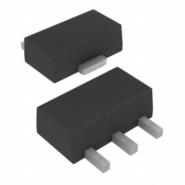
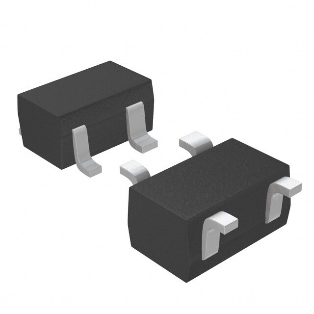
| 供应商器件封装 | SOT-23-5 |
| 其它名称 | LP2992IM525NOPB |
| 制造商产品页 | http://www.ti.com/general/docs/suppproductinfo.tsp?distId=10&orderablePartNumber=LP2992IM5-2.5/NOPB |
| 包装 | 带卷 (TR) |
| 商标 | Texas Instruments |
| 回动电压—最大值 | 850 mV |
| 安装类型 | 表面贴装 |
| 安装风格 | SMD/SMT |
| 封装 | Reel |
| 封装/外壳 | SC-74A,SOT-753 |
| 封装/箱体 | SOT-23-5 |
| 工作温度 | -40°C ~ 125°C |
| 工厂包装数量 | 1000 |
| 最大工作温度 | + 125 C |
| 最大输入电压 | 16 V |
| 最小工作温度 | - 40 C |
| 最小输入电压 | 2.2 V |
| 标准包装 | 1,000 |
| 电压-跌落(典型值) | 0.45V @ 250mA |
| 电压-输入 | 最高 16V |
| 电压-输出 | 2.5V |
| 电流-输出 | 250mA |
| 电流-限制(最小值) | - |
| 稳压器拓扑 | 正,固定式 |
| 稳压器数 | 1 |
| 类型 | Fixed-output Voltage Regulator |
| 系列 | LP2992 |
| 线路调整率 | 0.007 % |
| 设计资源 | http://www.digikey.com/product-highlights/cn/zh/texas-instruments-webench-design-center/3176 |
| 输出电压 | 2.5 V |
| 输出电压容差 | 4.5 % |
| 输出电流 | 250 mA |
| 输出端数量 | 1 Output |
| 输出类型 | Fixed |


- 商务部:美国ITC正式对集成电路等产品启动337调查
- 曝三星4nm工艺存在良率问题 高通将骁龙8 Gen1或转产台积电
- 太阳诱电将投资9.5亿元在常州建新厂生产MLCC 预计2023年完工
- 英特尔发布欧洲新工厂建设计划 深化IDM 2.0 战略
- 台积电先进制程称霸业界 有大客户加持明年业绩稳了
- 达到5530亿美元!SIA预计今年全球半导体销售额将创下新高
- 英特尔拟将自动驾驶子公司Mobileye上市 估值或超500亿美元
- 三星加码芯片和SET,合并消费电子和移动部门,撤换高东真等 CEO
- 三星电子宣布重大人事变动 还合并消费电子和移动部门
- 海关总署:前11个月进口集成电路产品价值2.52万亿元 增长14.8%


PDF Datasheet 数据手册内容提取
Product Order Technical Tools & Support & Reference Folder Now Documents Software Community Design LP2992 SNVS171J–NOVEMBER2001–REVISEDJANUARY2017 LP2992 Micropower 250-mA Low-Noise Ultra-Low-Dropout Regulator in SOT-23 and WSON Packages Designed for Use With Very Low-ESR Output Capacitors 1 Features 3 Description • InputVoltageRange:2.2Vto16V The LP2992 is a 250-mA, fixed-output voltage 1 regulator designed to provide ultra-low dropout and • OutputVoltageRange:1.5Vto5V lownoiseinbattery-poweredapplications. • WideSupplyVoltageRange(16-VMaximum) Using an optimized vertically integrated PNP (VIP) • OutputVoltageAccuracy1%(AGrade) process, the LP2992 delivers unequaled performance • Ultra-Low-DropoutVoltage in all specifications critical to battery-powered • Specified250-mAOutputCurrent designs: • Dropout voltage: Typically 450 mV at 250-mA • StableWithLow-ESROutputCapacitor load,and5mVat1-mAload. • <1-µAQuiescentCurrentWhenShutDown • Ground pin current: Typically 1500 µA at 250-mA • LowGroundPinCurrentatAllLoads load,and75µAat1-mAload. • HighPeakCurrentCapability • Enhanced stability: The LP2992 is stable with • LowZ :0.3-ΩTypical(10Hzto1MHz) output capacitor equivalent series resistance OUT (ESR) as low as 5 mΩ, which allows the use of • OvertemperatureandOvercurrentProtection ceramiccapacitorsontheoutput. • −40°Cto+125°CJunctionTemperatureRange • Sleep mode: Less than 1-µA quiescent current • SmallestPossibleSize(SOT-23,WSON whenON/OFF pinispulledlow. Package) • Smallest possible size: SOT-23 and WSON • RequiresMinimumExternalComponents packagesuseabsoluteminimumboardspace. • CustomVoltagesAvailable • Precision output: 1% tolerance output voltages available(Agrade). 2 Applications • Low noise: By adding a 10-nF bypass capacitor, outputnoisecanbereducedto30µV(typical). • CellularPhones • Multiple voltage options, from 1.5 V to 5 V, are • Palmtop/LaptopComputers available as standard products. Consult factory for • PersonalDigitalAssistants(PDA) customvoltages. • Camcorders,PersonalStereos,Cameras DeviceInformation(1) PARTNUMBER PACKAGE BODYSIZE(NOM) WSON(6) 3.29mm×2.92mm LP2992 SOT-23(5) 2.90mm×1.60mm (1) For all available packages, see the orderable addendum at theendofthedatasheet. SimplifiedSchematic VIN VOUT IN OUT CIN COUT LP2992 GND VON/OFF ON/OFF BYPASS ON OFF CBYPASS Copyright © 2017, Texas Instruments Incorporated 1 An IMPORTANT NOTICE at the end of this data sheet addresses availability, warranty, changes, use in safety-critical applications, intellectualpropertymattersandotherimportantdisclaimers.PRODUCTIONDATA.
LP2992 SNVS171J–NOVEMBER2001–REVISEDJANUARY2017 www.ti.com Table of Contents 1 Features.................................................................. 1 8 ApplicationandImplementation........................ 15 2 Applications........................................................... 1 8.1 ApplicationInformation............................................15 3 Description............................................................. 1 8.2 TypicalApplication .................................................15 4 RevisionHistory..................................................... 2 9 PowerSupplyRecommendations...................... 20 5 PinConfigurationandFunctions......................... 3 10 Layout................................................................... 21 6 Specifications......................................................... 4 10.1 LayoutGuidelines.................................................21 6.1 AbsoluteMaximumRatings......................................4 10.2 LayoutExamples...................................................21 6.2 ESDRatings..............................................................4 10.3 WSONMounting...................................................21 6.3 RecommendedOperatingConditions.......................4 11 DeviceandDocumentationSupport................. 22 6.4 ThermalInformation..................................................5 11.1 DocumentationSupport........................................22 6.5 ElectricalCharacteristics...........................................5 11.2 ReceivingNotificationofDocumentationUpdates22 6.6 TypicalCharacteristics..............................................7 11.3 CommunityResources..........................................22 7 DetailedDescription............................................ 13 11.4 Trademarks...........................................................22 7.1 Overview.................................................................13 11.5 ElectrostaticDischargeCaution............................22 7.2 FunctionalBlockDiagram.......................................13 11.6 Glossary................................................................22 7.3 FeatureDescription.................................................13 12 Mechanical,Packaging,andOrderable Information........................................................... 22 7.4 DeviceFunctionalModes........................................14 4 Revision History NOTE:Pagenumbersforpreviousrevisionsmaydifferfrompagenumbersinthecurrentversion. ChangesfromRevisionI(November2015)toRevisionJ Page • DeletedspecificvaluesfromcapacitorsinSimplifiedSchematicdrawing ............................................................................ 1 • AddedReceivingNotificationofDocumentationUpdates ................................................................................................... 22 ChangesfromRevisionH(January2015)toRevisionI Page • AddedtopnavigatoriconforTIDesign ................................................................................................................................. 1 • Changed"174.2°C/W"to"169.7°C/W"infootnote3toAbsMaxtable. ................................................................................ 4 • ChangedESDRatingstabletodifferentiatedifferentvaluesfordifferentpins/packages..................................................... 4 • Addednewfootnotes2and3toThermalInformationtable;updatethermalvaluesforDBV(SOT-23)package................5 • AddedPowerDissipationandEstimatingJunctionTemperaturesubsections ................................................................... 18 • Addedadditionalrelateddocumentlinks............................................................................................................................. 22 ChangesfromRevisionG(March2013)toRevisionH Page • AddedDeviceInformationandESDRatingstables,PinConfigurationandFunctions,FeatureDescription,Device FunctionalModes,ApplicationandImplementation,PowerSupplyRecommendations,Layout,Deviceand DocumentationSupport,andMechanical,Packaging,andOrderableInformationsections;updateThermalValues andpinnames........................................................................................................................................................................ 1 ChangesfromRevisionF(March2013)toRevisionG Page • ChangedChangedlayoutofNationalSemiconductordatasheettoTIformat ..................................................................... 1 2 SubmitDocumentationFeedback Copyright©2001–2017,TexasInstrumentsIncorporated ProductFolderLinks:LP2992
LP2992 www.ti.com SNVS171J–NOVEMBER2001–REVISEDJANUARY2017 5 Pin Configuration and Functions DBVPackage 5-PinSOT-23 TopView NGDPackage 6-PinWSON TopView PinFunctions PIN I/O DESCRIPTION NAME DBV NAME NGD BYPASS 4 BYPASS 1 I Bypasscapacitorforlow-noiseoperation. GND 2 GND 2 – Ground. IN 1 IN 4 I Unregulatedinputvoltage. – – N/C 5 – Nointernalconnection.ConnecttoGNDorleaveopen. Alowvoltageonthispindisablesthedevice,andtheregulatorenters ON/OFF 3 ON/OFF 3 I asleepmode.Ahighvoltageonthispinenablesthedevice. Regulatedoutputvoltage.Thispinrequiresanoutputcapacitorto OUT 5 OUT 6 O maintainstability.SeetheDetailedDesignProcedureforoutput capacitordetails. Theexposeddieattachpadonthebottomofthepackagemustbe Exposed connectedtoacopperthermalpadonthePCBatgroundpotential. — — DAP — thermalpad Connecttogroundpotentialorleavefloating.Donotconnecttoany potentialotherthanthesamegroundpotentialseenatdevicepin2. Copyright©2001–2017,TexasInstrumentsIncorporated SubmitDocumentationFeedback 3 ProductFolderLinks:LP2992
LP2992 SNVS171J–NOVEMBER2001–REVISEDJANUARY2017 www.ti.com 6 Specifications 6.1 Absolute Maximum Ratings overoperatingfree-airtemperaturerange(unlessotherwisenoted)(1)(2) MIN MAX UNIT Leadtemperature(soldering,5seconds) 260 °C Powerdissipation(3) InternallyLimited Inputsupplyvoltage(survival) −0.3 16 V Shutdowninputvoltage(survival) −0.3 16 V Outputvoltage(survival)(4) −0.3 9 V I (survival) Short-circuitprotected OUT Input-outputvoltage(survival)(5) −0.3 16 V Storagetemperature,T −65 150 °C stg (1) StressesbeyondthoselistedunderAbsoluteMaximumRatingsmaycausepermanentdamagetothedevice.Thesearestressratings only,whichdonotimplyfunctionaloperationofthedeviceattheseoranyotherconditionsbeyondthoseindicatedunderRecommended OperatingConditions.Exposuretoabsolute-maximum-ratedconditionsforextendedperiodsmayaffectdevicereliability. (2) IfMilitary-orAerospace-specifieddevicesarerequired,contacttheTexasInstrumentsSalesOffice/Distributorsforavailabilityand specifications. (3) Themaximumallowablepowerdissipationisafunctionofthemaximumjunctiontemperature,T ,thejunction-to-ambientthermal J(MAX) resistance,R ,andtheambienttemperature,T .Themaximumallowablepowerdissipationatanyambienttemperatureiscalculated θJA A using: P =(T –T )/R (MAX) J(MAX) A θJA WherethevalueofR fortheSOT-23packageis169.7°C/WinatypicalPCboardmountingandtheWSONpackageis72.3°C/W. θJA Exceedingthemaximumallowabledissipationcausesexcessivedietemperature,andtheregulatorgoesintothermalshutdown. (4) Ifusedinadual-supplysystemwheretheregulatorloadisreturnedtoanegativesupply,theLP2992outputmustbediode-clampedto ground. (5) TheoutputPNPstructurecontainsadiodebetweentheINtoOUTpinsthatisnormallyreverse-biased.ReversingthepolarityfromV IN toV turnsonthisdiode. OUT 6.2 ESD Ratings VALUE UNIT Pins3and4(SOT) ±1000 Electrostatic Humanbodymodel(HBM),per Pins1and3(WSON) V(ESD) discharge ANSI/ESDA/JEDECJS-001(1) Allpinsexcept3and4(SOT) V ±2000 Allpinsexcept1and3(WSON) (1) JEDECdocumentJEP155statesthat500-VHBMallowssafemanufacturingwithastandardESDcontrolprocess. 6.3 Recommended Operating Conditions overoperatingfree-airtemperaturerange(unlessotherwisenoted) MIN MAX UNIT V Inputsupplyvoltage 2.2(1) 16 V IN V ON/OFFinputvoltage 0 V V ON/OFF IN I Outputcurrent 250 mA OUT T Operatingjunctiontemperature –40 125 °C J (1) RecommendedminimumV isthegreaterof2.2VorV +rateddropoutvoltage(maximum)foroperatingloadcurrent. IN OUT 4 SubmitDocumentationFeedback Copyright©2001–2017,TexasInstrumentsIncorporated ProductFolderLinks:LP2992
LP2992 www.ti.com SNVS171J–NOVEMBER2001–REVISEDJANUARY2017 6.4 Thermal Information LP2992 THERMALMETRIC(1) DBV(SOT-23) NGD(WSON)(2) UNIT 5PINS 6PINS R (3) Junction-to-ambientthermalresistance 169.7 72.3 °C/W θJA R Junction-to-case(top)thermalresistance,HighK 122.6 81.6 °C/W θJC(top) R Junction-to-boardthermalresistance 29.9 39.5 °C/W θJB ψ Junction-to-topcharacterizationparameter 16.7 2.0 °C/W JT ψ Junction-to-boardcharacterizationparameter 29.4 39.2 °C/W JB R Junction-to-case(bottom)thermalresistance n/a 11.6 °C/W θJC(bot) (1) Formoreinformationabouttraditionalandnewthermalmetrics,seetheSemiconductorandICPackageThermalMetrics. (2) ThePCBfortheNGD(WSON)packageR includestwo(2)thermalviasundertheexposedthermalpadperEIA/JEDECJESD51-5. θJA (3) ThermalresistancevalueR isbasedontheEIA/JEDECHigh-Kprintedcircuitboarddefinedby:JESD51-7-HighEffectiveThermal θJA ConductivityTestBoardforLeadedSurfaceMountPackages. 6.5 Electrical Characteristics Unlessotherwisespecified:V =V +1V,I =1mA,C =1µF,C =4.7µF,V =2V.MIN(minimum)and IN OUT(NOM) L IN OUT ON/OFF MAX(maximum)limitsapplyovertherecommendedoperatingtemperaturerangeunlessotherwisenoted;typicallimitsapply forT =T =25°C. A J LP2992AI-X.X(1) LP2992I-X.X(1) PARAMETER TESTCONDITIONS TYP UNIT MIN MAX MIN MAX I =1mA,T =25°C −1 1 −1.5 1.5 L J 1mA≤I ≤50mA,T =25°C −1.5 1.5 −2.5 2.5 L J ΔV Outputvoltagetolerance 1mA≤I ≤50mA −2.5 2.5 −3.5 3.5 %V OUT L NOM 1mA≤I ≤250mA,T =25°C −3.5 3.5 −4 4 L J 1mA≤I ≤250mA −4.5 4.5 −5 5 L V +1V≤V ≤16V OUT(NOM) IN 0.007 0.014 0.014 ΔVOUT/ΔVIN Outputvoltagelineregulation TJ=25°C %/V V +1V≤V ≤16V 0.032 0.032 OUT(NOM) IN V (min) Minimuminputvoltagerequiredtomaintainoutputregulation 2.05 2.2 2.2 V IN I =0mA,T =25°C 0.5 2.5 2.5 L J I =0mA 4 4 L I =1mA,T =25°C 5 9 9 L J I =1mA 12 12 L I =50mA,T =25°C 100 125 125 V –V Dropoutvoltage(2) L J mV IN OUT I =50mA 180 180 L I =150mA,T =25°C 260 325 325 L J I =150mA 470 470 L I =250mA,T =25°C 450 575 575 L J I =250mA 850 850 L (1) Limitsare100%productiontestedat25°C.Limitsovertheoperatingtemperaturerangearespecifiedthroughcorrelationusing StatisticalQualityControl(SQC)methods.ThelimitsareusedtocalculateTI'sAverageOutgoingQualityLevel(AOQL). (2) V mustbethegreaterof2.2VorV +dropoutvoltagetomaintainoutputregulation.Dropoutvoltageisdefinedastheinput-to- IN OUT(NOM) outputdifferentialatwhichtheoutputvoltagedrops2%belowthevaluemeasuredwitha1-Vdifferential. Copyright©2001–2017,TexasInstrumentsIncorporated SubmitDocumentationFeedback 5 ProductFolderLinks:LP2992
LP2992 SNVS171J–NOVEMBER2001–REVISEDJANUARY2017 www.ti.com Electrical Characteristics (continued) Unlessotherwisespecified:V =V +1V,I =1mA,C =1µF,C =4.7µF,V =2V.MIN(minimum)and IN OUT(NOM) L IN OUT ON/OFF MAX(maximum)limitsapplyovertherecommendedoperatingtemperaturerangeunlessotherwisenoted;typicallimitsapply forT =T =25°C. A J LP2992AI-X.X(1) LP2992I-X.X(1) PARAMETER TESTCONDITIONS TYP UNIT MIN MAX MIN MAX I =0mA,T =25°C 65 95 95 L J I =0mA 125 125 L I =1mA,T =25°C 75 110 110 L J I =1mA 170 170 L I =50mA,T =25°C 350 600 600 L J I =50mA 1000 1000 L I Groundpincurrent µA GND I =150mA,T =25°C 850 1500 1500 L J I =150mA 2500 2500 L I =250mA,T =25°C 1500 2300 2300 L J I =250mA 4000 4000 L V <0.3V,T =25°C 0.01 0.8 0.8 ON/OFF J V <0.15V 0.05 2 2 ON/OFF High=O/PON 1.4 1.6 1.6 V ON/OFFinputvoltage(3) V ON/OFF Low=O/POFF 0.55 0.15 0.15 V =0 0.01 –2 –2 ON/OFF I ON/OFFinputcurrent µA ON/OFF V =5V 5 15 15 ON/OFF Bandwidth=300Hzto50kHz e Outputnoisevoltage(RMS) C =10µF 30 µV n OUT C =10nF BYPASS f=1kHz,C =10nF ΔV /ΔV Ripplerejection BYPASS 45 dB OUT IN C =10µF OUT I (SC) Short-circuitcurrent R =0(steadystate)(4) 400 mA O L I (PK) Peakoutputcurrent V ≥V –5% 350 mA O OUT O(NOM) (3) TheON/OFFinputmustbeproperlydriventopreventpossiblemis-operation.Fordetails,seeOperationwithON/OFFControl. (4) TheLP2992hasthermalfoldbackcurrentlimitingwhichallowsahighpeakcurrentwhenV >0.5V,andthenreducesthemaximum OUT outputcurrentasV isforcedtoground(seeTypicalCharacteristicscurves). OUT 6 SubmitDocumentationFeedback Copyright©2001–2017,TexasInstrumentsIncorporated ProductFolderLinks:LP2992
LP2992 www.ti.com SNVS171J–NOVEMBER2001–REVISEDJANUARY2017 6.6 Typical Characteristics Unlessotherwisespecified:C =1µF,C =4.7µF,V =V +1V,T =25°C,ON/OFFpinistiedtotheINpin. IN OUT IN OUT(NOM) A Figure1.VOUTvsTemperature Figure2.Short-CircuitCurrent Figure3.Short-CircuitCurrent Figure4.Short-CircuitCurrentvsOutputVoltage Figure5.RippleRejection Figure6.RippleRejection Copyright©2001–2017,TexasInstrumentsIncorporated SubmitDocumentationFeedback 7 ProductFolderLinks:LP2992
LP2992 SNVS171J–NOVEMBER2001–REVISEDJANUARY2017 www.ti.com Typical Characteristics (continued) Unlessotherwisespecified:C =1µF,C =4.7µF,V =V +1V,T =25°C,ON/OFFpinistiedtotheINpin. IN OUT IN OUT(NOM) A Figure7.RippleRejection Figure8.RippleRejection Figure9.RippleRejection Figure10.RippleRejection Figure11.RippleRejection Figure12.RippleRejection 8 SubmitDocumentationFeedback Copyright©2001–2017,TexasInstrumentsIncorporated ProductFolderLinks:LP2992
LP2992 www.ti.com SNVS171J–NOVEMBER2001–REVISEDJANUARY2017 Typical Characteristics (continued) Unlessotherwisespecified:C =1µF,C =4.7µF,V =V +1V,T =25°C,ON/OFFpinistiedtotheINpin. IN OUT IN OUT(NOM) A Figure13.RippleRejection Figure14.OutputImpedancevsFrequency Figure15.OutputImpedancevsFrequency Figure16.OutputNoiseDensity Figure17.OutputNoiseDensity Figure18.GNDPinvsLoadCurrent Copyright©2001–2017,TexasInstrumentsIncorporated SubmitDocumentationFeedback 9 ProductFolderLinks:LP2992
LP2992 SNVS171J–NOVEMBER2001–REVISEDJANUARY2017 www.ti.com Typical Characteristics (continued) Unlessotherwisespecified:C =1µF,C =4.7µF,V =V +1V,T =25°C,ON/OFFpinistiedtotheINpin. IN OUT IN OUT(NOM) A Figure19.DropoutVoltagevsTemperature Figure20.InputCurrentvsPin Figure21.I vsLoadandTemperature Figure22.InstantaneousShort-CircuitCurrent GND Figure23.LoadTransientResponse Figure24.LoadTransientResponse 10 SubmitDocumentationFeedback Copyright©2001–2017,TexasInstrumentsIncorporated ProductFolderLinks:LP2992
LP2992 www.ti.com SNVS171J–NOVEMBER2001–REVISEDJANUARY2017 Typical Characteristics (continued) Unlessotherwisespecified:C =1µF,C =4.7µF,V =V +1V,T =25°C,ON/OFFpinistiedtotheINpin. IN OUT IN OUT(NOM) A Figure25.LoadTransientResponse Figure26.LineTransientResponse Figure27.LineTransientResponse Figure28.LineTransientResponse Figure29.LineTransientResponse Figure30.TurnonTime Copyright©2001–2017,TexasInstrumentsIncorporated SubmitDocumentationFeedback 11 ProductFolderLinks:LP2992
LP2992 SNVS171J–NOVEMBER2001–REVISEDJANUARY2017 www.ti.com Typical Characteristics (continued) Unlessotherwisespecified:C =1µF,C =4.7µF,V =V +1V,T =25°C,ON/OFFpinistiedtotheINpin. IN OUT IN OUT(NOM) A Figure31.TurnonTime Figure32.TurnonTime Figure33.TurnonTime 12 SubmitDocumentationFeedback Copyright©2001–2017,TexasInstrumentsIncorporated ProductFolderLinks:LP2992
LP2992 www.ti.com SNVS171J–NOVEMBER2001–REVISEDJANUARY2017 7 Detailed Description 7.1 Overview The LP2992 family of fixed-output, ultralow-dropout, and low-noise regulators offer exceptional and cost-effective performance for battery-powered applications. Available in output voltages from 1.5 V to 5 V, the family has an output tolerance of 1% for the A version and is capable of delivering 250-mA continuous load current. Using an optimized vertically integrated PNP (VIP) process, the LP2992 delivers unequaled performance. The dropout voltageandtheGNDpincurrentwith250mAofloadcurrentaretypically450mVand1500 µA,respectively. 7.2 Functional Block Diagram 7.3 Feature Description 7.3.1 SleepMode When the ON/OFF pin is pulled low, the LP2992 enters a sleep mode, and less than 1-µA quiescent current is consumed. This function is designed for the application which needs a sleep mode to effectively enhance battery lifecycle. 7.3.2 LowGroundCurrent The LP2992 uses a vertical PNP process which allows for quiescent currents which are considerably lower than those associated with traditional lateral PNP regulators, typically 1500 µA at 250-mA load and 75 µA at 1-mA load. 7.3.3 LowNoise The LP2992 includes a low-noise reference ensuring minimal noise during operation because the internal reference is normally the dominant term in a noise analysis. Further noise reduction can be achieved by adding an external bypass capacitor between the BYPASS pin and the GND pin. For more detailed information on noise reductionusingtheBYPASSpin,seeNoiseBypassCapacitor. 7.3.4 EnhancedStability The LP2992 is designed specifically to work with ceramic output capacitors using circuitry that allows the regulator to be stable across the entire range of output current with an output capacitor whose ESR is as low as 5mΩ.Foroutputcapacitorrequirements,seeOutputCapacitor. Copyright©2001–2017,TexasInstrumentsIncorporated SubmitDocumentationFeedback 13 ProductFolderLinks:LP2992
LP2992 SNVS171J–NOVEMBER2001–REVISEDJANUARY2017 www.ti.com Feature Description (continued) 7.3.5 OvercurrentProtection The internal current-limit circuit is used to protect the LDO against high-current faults or shorting events. The LDO is not designed to operate in a steady-state current limit. During a current-limit event, the LDO sources constant current. Therefore, the output voltage falls when the output impedance decreases. Note also that if a current limit occurs and the resulting output voltage is low, excessive power may be dissipated across the LDO, resultinginathermalshutdownoftheoutput. The LP2992 is featured with the foldback current limit that allows a high peak current when V > 0.5 V, and OUT thenreducesthemaximumoutputcurrentasV isforcedtoground. OUT 7.3.6 OvertemperatureProtection The LP2992 is designed with the thermal shutdown circuitry to turn off the output when excessive heat is dissipated in the LDO. The internal protection circuitry of the LP2992 is designed to protect against thermal overloadconditions.Continuouslyrunningthedeviceintothermalshutdowndegradesitsreliability. 7.4 Device Functional Modes 7.4.1 OperationwithV +0.9V ≥ V ≥16V OUT(TARGET) IN The LP2992 operates if the input voltage is equal to or exceeds V + 0.9 V. At input voltages below the OUT(TARGET) minimumV requirement,thedevicedoesnotoperatecorrectlyandoutputvoltagemaynotreachatargetvalue. IN 7.4.2 OperationwithON/OFF Control If the voltage on the ON/OFF pin is less than 0.15 V, the device is disabled and, in this shutdown state, current does not exceed 2 µA. Raising the voltage at the ON/OFF pin above 1.6 V initiates the start-up sequence of the device. If this feature is not to be used, the ON/OFF input must be tied to V to keep the regulator output on at IN alltimes. To assure proper operation, the signal source used to drive the ON/OFF input must be able to swing above and below the specified turnon/turnoff voltage thresholds listed in the Electrical Characteristics section under V . ON/OFF To prevent mis-operation, the turnon (and turnoff) voltage signals applied to the ON/OFF input must have a slew ratewhichis≥ 40mV/µs. CAUTION The regulator output voltage can not be ensured if a slow-moving AC (or DC) signal is applied that is in the range between the specified turnon and turnoff voltages listed undertheelectricalspecificationV (seeElectricalCharacteristics). ON/OFF 14 SubmitDocumentationFeedback Copyright©2001–2017,TexasInstrumentsIncorporated ProductFolderLinks:LP2992
LP2992 www.ti.com SNVS171J–NOVEMBER2001–REVISEDJANUARY2017 8 Application and Implementation NOTE Information in the following applications sections is not part of the TI component specification, and TI does not warrant its accuracy or completeness. TI’s customers are responsible for determining suitability of components for their purposes. Customers should validateandtesttheirdesignimplementationtoconfirmsystemfunctionality. 8.1 Application Information The LP2992 is a 250-mA, fixed-output voltage regulator designed to provide ultralow-dropout and low noise in battery powered applications. The device is stable with output capacitor equivalent series resistance (ESR) as lowas5mΩ whichallowstheuseofceramiccapacitorsontheoutput. At 250-mA loading, the dropout voltage of the LP2992 is 850 mV maximum over temperature; thus, 1000-mV headroom is sufficient for operation over input and output voltage accuracy. The efficiency of the LP2992 in this configurationisV /V =76.7%.Toachievethesmallestformfactor,theSOT-23packageisselected. OUT IN Input and output capacitors are selected in accordance with Capacitor Characteristics. Ceramic capacitance of 1 µF for the input and that of 4.7 µF for the output are selected. With efficiency of 76.7% and a 250-mA load current,theinternalpowerdissipationis250mW,whichcorrespondsto43.55°Cjunctiontemperatureriseforthe SOT-23package.Tominimizenoise,abypasscapacitor(C )of0.01 µFisselected. BYPASS 8.2 Typical Application *ON/OFFinputmustbeactivelyterminated.TietotheINpinifthisfunctionisnottobeused. **Minimumcapacitanceisshowntoensurestability(maybeincreasedwithoutlimit).Ceramiccapacitorrequiredfor output(seeOutputCapacitor). ***Reducesoutputnoise(maybeomittedifapplicationisnotnoisecritical).Useceramicorfilmtypewithverylow leakagecurrent(seeCapacitorCharacteristics). Figure34. BasicApplicationCircuit Copyright©2001–2017,TexasInstrumentsIncorporated SubmitDocumentationFeedback 15 ProductFolderLinks:LP2992
LP2992 SNVS171J–NOVEMBER2001–REVISEDJANUARY2017 www.ti.com Typical Application (continued) 8.2.1 DesignRequirements Forbasicdesignparameters,seeTable1. Table1.DesignParameters DESIGNPARAMETER VALUE Inputvoltage 4.3V Outputvoltage 3.3V 150mA(maximum) Outputcurrent 1mA(minimum) Outputcapacitorrange 4.7µF 8.2.2 DetailedDesignProcedure 8.2.2.1 ExternalCapacitors Like any low-dropout regulator, the LP2992 requires external capacitors for regulator stability. These capacitors mustbecorrectlyselectedforgoodperformance. 8.2.2.1.1 InputCapacitor Aninputcapacitorwhosecapacitanceis≥ 1 µFisrequiredbetweentheLP2992inputandground(theamountof capacitancemaybeincreasedwithoutlimit). This capacitor must be located a distance of not more than 1 cm from the IN pin and returned to a clean analog ground.Anygoodqualityceramic,tantalum,orfilmcapacitormaybeusedattheinput. NOTE Tantalum capacitors can suffer catastrophic failure due to surge current when connected to a low-impedance source of power (like a battery or very large capacitor). If a tantalum capacitor is used at the input, it must be specified by the manufacturer to have a surge currentratingsufficientfortheapplication. There are no requirements for ESR on the input capacitor, but tolerance and temperature coefficient must be considered when selecting the capacitor to ensure the capacitance is ≥ 1 µF over the entire operating temperaturerange. 8.2.2.1.2 OutputCapacitor The LP2992 is designed specifically to work with ceramic output capacitors, using circuitry that allows the regulator to be stable across the entire range of output current with an output capacitor whose ESR is as low as 5 mΩ. It may also be possible to use tantalum or film capacitors at the output, but these are not as attractive for reasonsofsizeandcost(seeCapacitorCharacteristics). The output capacitor must meet the requirement for minimum amount of capacitance and also have an ESR value which is within the stable range. Curves are provided which show the stable ESR range as a function of loadcurrent(seeFigure35). 16 SubmitDocumentationFeedback Copyright©2001–2017,TexasInstrumentsIncorporated ProductFolderLinks:LP2992
LP2992 www.ti.com SNVS171J–NOVEMBER2001–REVISEDJANUARY2017 Figure35. StableESRRangevsLoadCurrent The output capacitor must maintain its ESR within the stable region over the full operating temperature range of theapplicationtoassurestability. TheLP2992requiresaminimumof4.7µFontheoutput(outputcapacitorsizecanbeincreasedwithoutlimit). It is important to remember that capacitor tolerance and variation with temperature must be taken into consideration when selecting an output capacitor so that the minimum required amount of output capacitance is provided over the full operating temperature range. It must be noted that ceramic capacitors can exhibit large changesincapacitancewithtemperature(seeCapacitorCharacteristics). The output capacitor must be located not more than 1 cm from the output pin and returned to a clean analog ground. 8.2.2.1.3 NoiseBypassCapacitor Connecting a 10-nF capacitor to the BYPASS pin significantly reduces noise on the regulator output. It should be notedthatthecapacitorisconnecteddirectlytoahigh-impedancecircuitinthebandgapreference. Because this circuit has only a few microamperes flowing in it, any significant loading on this node causes a change in the regulated output voltage. For this reason, dc leakage current through the noise bypass capacitor mustneverexceed100nA,andmustbekeptaslowaspossibleforbestoutputvoltageaccuracy. The types of capacitors best suited for the noise bypass capacitor are ceramic and film. High-quality ceramic capacitors with either NPO or COG dielectric typically have very low leakage. 10-nF polypropolene and polycarbonate film capacitors are available in small surface-mount packages and typically have extremely low leakagecurrent. 8.2.2.2 CapacitorCharacteristics The LP2992 was designed to work with ceramic capacitors on the output to take advantage of the benefits they offer. For capacitance values in the 2.2-µF to 10-µF range, ceramics are the least expensive and also have the lowest ESR values (which makes them best for eliminating high-frequency noise). The ESR of a typical 4.7-µF ceramic capacitor is in the range of 5 mΩ to 10 mΩ, which easily meets the ESR limits required for stability by theLP2992. One disadvantage of ceramic capacitors is that their capacitance can vary with temperature. Most large value ceramic capacitors (≥ 2.2 µF) are manufactured with the Z5U or Y5V temperature characteristic, which results in thecapacitancedroppingbymorethan50%asthetemperaturegoesfrom25°Cto85°C. Thiscouldcauseproblemsifa4.7-µFcapacitorwereusedontheoutputbecauseitdropsdowntoapproximately 2.3 µF at high ambient temperatures (which could cause the LP2992 to oscillate). If Z5U or Y5V capacitors are usedontheoutput,aminimumcapacitancevalueof10 µFmustbeobserved. A better choice for temperature coefficient in ceramic capacitors is X7R, which holds the capacitance within ±15%.Unfortunately,thelargervaluesofcapacitancearenotofferedbyallmanufacturersintheX7Rdielectric. Copyright©2001–2017,TexasInstrumentsIncorporated SubmitDocumentationFeedback 17 ProductFolderLinks:LP2992
LP2992 SNVS171J–NOVEMBER2001–REVISEDJANUARY2017 www.ti.com 8.2.2.2.1 Tantalum Tantalum capacitors are less desirable than ceramics for use as output capacitors because they are more expensivewhencomparingequivalentcapacitanceandvoltageratingsinthe1-µFto4.7-µFrange. Another important consideration is that tantalum capacitors have higher ESR values than equivalent size ceramics. This means that while it may be possible to find a Tantalum capacitor with an ESR value within the stable range, it would have to be larger in capacitance (which means bigger and more costly) than a ceramic capacitorwiththesameESRvalue. It should also be noted that the ESR of a typical tantalum increases about 2:1 as the temperature goes from 25°Cdownto−40°C,sosomeguardbandmustbeallowed. 8.2.2.3 ReverseInput-OutputVoltage The PNP power transistor used as the pass element in the LP2992 has an inherent diode connected between the regulator output and input. During normal operation (where the input voltage is higher than the output) this diodeisreverse-biased. However, if the output is pulled above the input, this diode turns ON and current flows into the regulator output. In such cases, a parasitic SCR can latch which allows a high current to flow into V (and out the ground pin), IN whichcandamagethepart. In any application where the output may be pulled above the input, an external Schottky diode must be connected from V to V (cathode on V , anode on V ), to limit the reverse voltage across the LP2992 to IN OUT IN OUT 0.3V(seeAbsoluteMaximumRatings). 8.2.2.4 PowerDissipation Knowing the device power dissipation and proper sizing of the thermal plane connected to the tab or pad is critical to ensuring reliable operation. Device power dissipation depends on input voltage, output voltage, and loadconditionsandcanbecalculatedwithEquation1. P =(V –V )×I (1) D(MAX) IN(MAX) OUT OUT Power dissipation can be minimized, and greater efficiency can be achieved, by using the lowest available voltage drop option that would still be greater than the dropout voltage (V ). However, keep in mind that higher DO voltagedropsresultinbetterdynamic(thatis,PSRRandtransient)performance. On the WSON (NGD) package, the primary conduction path for heat is through the exposed power pad to the PCB. To ensure the device does not overheat, connect the exposed pad, through thermal vias, to an internal groundplanewithanappropriateamountofcopperPCBarea. On the SOT-23 (DBV) package, the primary conduction path for heat is through the pins to the PCB. The maximum allowable junction temperature (T )determines maximum power dissipation allowed (P ) for J(MAX) D(MAX) thedevicepackage. Power dissipation and junction temperature are most often related by the junction-to-ambient thermal resistance (R of the combined PCB and device package and the temperature of the ambient air (T ), according to θJA) A Equation2orEquation2: T =T +(R ×P ) (2) J(MAX) A(MAX) θJA D(MAX) P =T –T /R (3) D J(MAX) A(MAX) θJA Unfortunately, this R is highly dependent on the heat-spreading capability of the particular PCB design, and θJA therefore varies according to the total copper area, copper weight, and location of the planes. The R recorded θJA in Thermal Information is determined by the specific EIA/JEDEC JESD51-7 standard for PCB and copper- spreading area, and is to be used only as a relative measure of package thermal performance. For a well- designed thermal layout, R is actually the sum of the package junction-to-case (bottom) thermal resistance θJA (R )plusthethermalresistancecontributionbythePCBcopperareaactingasaheatsink. θJCbot 18 SubmitDocumentationFeedback Copyright©2001–2017,TexasInstrumentsIncorporated ProductFolderLinks:LP2992
LP2992 www.ti.com SNVS171J–NOVEMBER2001–REVISEDJANUARY2017 8.2.2.5 EstimatingJunctionTemperature The EIA/JEDEC standard recommends the use of psi (Ψ) thermal characteristics to estimate the junction temperatures of surface mount devices on a typical PCB board application. These characteristics are not true thermal resistance values, but rather package specific thermal characteristics that offer practical and relative means of estimating junction temperatures. These psi metrics are determined to be significantly independent of copper-spreading area. The key thermal characteristics (Ψ and Ψ ) are given in Thermal Information and are JT JB usedinaccordancewithEquation4orEquation5. T =T +(Ψ ×P ) J(MAX) TOP JT D(MAX) where • P isexplainedinEquation3 D(MAX) • T isthetemperaturemeasuredatthecenter-topofthedevicepackage. (4) TOP T =T +(Ψ ×P ) J(MAX) BOARD JB D(MAX) where • P isexplainedinEquation3. D(MAX) • T isthePCBsurfacetemperaturemeasured1-mmfromthedevicepackageandcenteredonthe BOARD packageedge. (5) Formoreinformationaboutthethermalcharacteristics Ψ and Ψ ,seeSemiconductorandICPackageThermal JT JB Metrics; for more information about measuring T and T , Using New Thermal Metrics(SBVA025); and for TOP BOARD more information about the EIA/JEDEC JESD51 PCB used for validating R , see Thermal Characteristics of θJA LinearandLogicPackagesUsingJEDECPCBDesigns.Theseapplicationnotesareavailableatwww.ti.com. Copyright©2001–2017,TexasInstrumentsIncorporated SubmitDocumentationFeedback 19 ProductFolderLinks:LP2992
LP2992 SNVS171J–NOVEMBER2001–REVISEDJANUARY2017 www.ti.com 8.2.3 ApplicationCurves Figure36.LoadTransientResponse Figure37.LoadTransientResponse Figure38.LineTransientResponse Figure39.LineTransientResponse Figure40.TurnonTime Figure41.TurnonTime 9 Power Supply Recommendations The LP2992 is designed to operate from an input voltage supply range from 2.2 V to 16 V. The input voltage rangeprovidestheadequateheadroominorderforthedevicetohavearegulatedoutput.Thisinputsupplymust be well regulated. If the input supply is noisy, additional input capacitors with low ESR can help to improve the outputnoiseperformance. 20 SubmitDocumentationFeedback Copyright©2001–2017,TexasInstrumentsIncorporated ProductFolderLinks:LP2992
LP2992 www.ti.com SNVS171J–NOVEMBER2001–REVISEDJANUARY2017 10 Layout 10.1 Layout Guidelines For best overall performance, place all circuit components on the same side of the circuit board and as near as practical to the respective LDO pin connections. Place ground return connections to the input and output capacitors,andtotheLDOgroundpinascloseaspossibletoeachother,connectedbyawide,component-side, copper surface. The use of vias and long traces to create LDO circuit connections is strongly discouraged and negatively affects system performance. This grounding and layout scheme minimizes inductive parasitics, and therebyreducesload-currenttransients,minimizesnoise,andincreasescircuitstability. TIalsorecommendsagroundreferenceplaneeitherembeddedinthePCBitselforlocatedonthebottomsideof the PCB opposite the components. This reference plane serves to assure accuracy of the output voltage, shield noise,andbehavessimilartoathermalplanetospread(orsink)heatfromtheLDOdevice.Inmostapplications, thisgroundplaneisnecessarytomeetthermalrequirements. 10.2 Layout Examples VIN VOUT 1 IN OUT 5 C C IN OUT 2 GND Power Ground C BYPASS ON/ V 3 BYPASS 4 ON/OFF OFF Figure42. LP2992SOT-23PackageTypicalLayout VBYPASS 1 6 VOUT CBYPASS COUT Power Ground 2 GND 5 C IN VON/OFF 3 4 VIN Figure43. LP2992WSONPackageTypicalLayout 10.3 WSON Mounting The WSON package requires specific mounting techniques which are detailed in AN-1187 Leadless Leadframe Package (LLP). Referring to the section PCB Design Recommendations, note that the pad style which must be usedwiththeWSONpackageistheNSMD(non-soldermaskdefined)type. The thermal dissipation of the WSON package is directly related to the printed circuit board construction and the amountofadditionalcopperarea. Copyright©2001–2017,TexasInstrumentsIncorporated SubmitDocumentationFeedback 21 ProductFolderLinks:LP2992
LP2992 SNVS171J–NOVEMBER2001–REVISEDJANUARY2017 www.ti.com 11 Device and Documentation Support 11.1 Documentation Support 11.1.1 RelatedDocumentation Forrelateddocumentationseethefollowing: • AN-1187LeadlessLeadframePackage(LLP) • SemiconductorandICPackageThermalMetrics • UsingNewThermalMetrics(SBVA025) • ThermalCharacteristicsofLinearandLogicPackagesUsingJEDECPCBDesigns 11.2 Receiving Notification of Documentation Updates To receive notification of documentation updates, navigate to the device product folder on ti.com. In the upper right corner, click on Alert me to register and receive a weekly digest of any product information that has changed.Forchangedetails,reviewtherevisionhistoryincludedinanyreviseddocument. 11.3 Community Resources The following links connect to TI community resources. Linked contents are provided "AS IS" by the respective contributors. They do not constitute TI specifications and do not necessarily reflect TI's views; see TI's Terms of Use. TIE2E™OnlineCommunity TI'sEngineer-to-Engineer(E2E)Community.Createdtofostercollaboration amongengineers.Ate2e.ti.com,youcanaskquestions,shareknowledge,exploreideasandhelp solveproblemswithfellowengineers. DesignSupport TI'sDesignSupport QuicklyfindhelpfulE2Eforumsalongwithdesignsupporttoolsand contactinformationfortechnicalsupport. 11.4 Trademarks E2EisatrademarkofTexasInstruments. Allothertrademarksarethepropertyoftheirrespectiveowners. 11.5 Electrostatic Discharge Caution Thesedeviceshavelimitedbuilt-inESDprotection.Theleadsshouldbeshortedtogetherorthedeviceplacedinconductivefoam duringstorageorhandlingtopreventelectrostaticdamagetotheMOSgates. 11.6 Glossary SLYZ022—TIGlossary. Thisglossarylistsandexplainsterms,acronyms,anddefinitions. 12 Mechanical, Packaging, and Orderable Information The following pages include mechanical, packaging, and orderable information. This information is the most current data available for the designated devices. This data is subject to change without notice and revision of thisdocument.Forbrowser-basedversionsofthisdatasheet,refertotheleft-handnavigation. 22 SubmitDocumentationFeedback Copyright©2001–2017,TexasInstrumentsIncorporated ProductFolderLinks:LP2992
PACKAGE OPTION ADDENDUM www.ti.com 6-Feb-2020 PACKAGING INFORMATION Orderable Device Status Package Type Package Pins Package Eco Plan Lead/Ball Finish MSL Peak Temp Op Temp (°C) Device Marking Samples (1) Drawing Qty (2) (6) (3) (4/5) LP2992AILD-1.5/NOPB ACTIVE WSON NGD 6 1000 Green (RoHS SN Level-3-260C-168 HR -40 to 125 L011A & no Sb/Br) LP2992AILD-1.8/NOPB ACTIVE WSON NGD 6 1000 Green (RoHS NIPDAU | SN Level-3-260C-168 HR -40 to 125 L012A & no Sb/Br) LP2992AILD-3.3/NOPB ACTIVE WSON NGD 6 1000 Green (RoHS NIPDAU | SN Level-3-260C-168 HR -40 to 125 L014A & no Sb/Br) LP2992AILD-5.0/NOPB ACTIVE WSON NGD 6 1000 Green (RoHS NIPDAU | SN Level-3-260C-168 HR -40 to 125 L015A & no Sb/Br) LP2992AILDX-3.3/NOPB ACTIVE WSON NGD 6 4500 Green (RoHS NIPDAU | SN Level-3-260C-168 HR -40 to 125 L014A & no Sb/Br) LP2992AILDX-5.0/NOPB ACTIVE WSON NGD 6 4500 Green (RoHS NIPDAU | SN Level-3-260C-168 HR -40 to 125 L015A & no Sb/Br) LP2992AIM5-1.5/NOPB ACTIVE SOT-23 DBV 5 1000 Green (RoHS SN Level-1-260C-UNLIM -40 to 125 LFBA & no Sb/Br) LP2992AIM5-1.8/NOPB ACTIVE SOT-23 DBV 5 1000 Green (RoHS SN Level-1-260C-UNLIM -40 to 125 LFCA & no Sb/Br) LP2992AIM5-2.5 NRND SOT-23 DBV 5 1000 TBD Call TI Call TI -40 to 125 LFDA LP2992AIM5-2.5/NOPB ACTIVE SOT-23 DBV 5 1000 Green (RoHS SN Level-1-260C-UNLIM -40 to 125 LFDA & no Sb/Br) LP2992AIM5-3.3 NRND SOT-23 DBV 5 1000 TBD Call TI Call TI -40 to 125 LFEA LP2992AIM5-3.3/NOPB ACTIVE SOT-23 DBV 5 1000 Green (RoHS SN Level-1-260C-UNLIM -40 to 125 LFEA & no Sb/Br) LP2992AIM5-5.0/NOPB ACTIVE SOT-23 DBV 5 1000 Green (RoHS SN Level-1-260C-UNLIM -40 to 125 LFFA & no Sb/Br) LP2992AIM5X-1.5/NOPB ACTIVE SOT-23 DBV 5 3000 Green (RoHS SN Level-1-260C-UNLIM -40 to 125 LFBA & no Sb/Br) LP2992AIM5X-1.8/NOPB ACTIVE SOT-23 DBV 5 3000 Green (RoHS SN Level-1-260C-UNLIM -40 to 125 LFCA & no Sb/Br) LP2992AIM5X-2.5/NOPB ACTIVE SOT-23 DBV 5 3000 Green (RoHS SN Level-1-260C-UNLIM -40 to 125 LFDA & no Sb/Br) LP2992AIM5X-3.3/NOPB ACTIVE SOT-23 DBV 5 3000 Green (RoHS SN Level-1-260C-UNLIM -40 to 125 LFEA & no Sb/Br) LP2992AIM5X-5.0/NOPB ACTIVE SOT-23 DBV 5 3000 Green (RoHS SN Level-1-260C-UNLIM -40 to 125 LFFA & no Sb/Br) Addendum-Page 1
PACKAGE OPTION ADDENDUM www.ti.com 6-Feb-2020 Orderable Device Status Package Type Package Pins Package Eco Plan Lead/Ball Finish MSL Peak Temp Op Temp (°C) Device Marking Samples (1) Drawing Qty (2) (6) (3) (4/5) LP2992ILD-1.8/NOPB ACTIVE WSON NGD 6 1000 Green (RoHS NIPDAU | SN Level-3-260C-168 HR -40 to 125 L012A & no Sb/Br) B LP2992ILD-2.5/NOPB ACTIVE WSON NGD 6 1000 Green (RoHS SN Level-3-260C-168 HR -40 to 125 L013A & no Sb/Br) B LP2992ILD-3.3/NOPB ACTIVE WSON NGD 6 1000 Green (RoHS NIPDAU | SN Level-3-260C-168 HR -40 to 125 L014A & no Sb/Br) B LP2992ILD-5.0/NOPB ACTIVE WSON NGD 6 1000 Green (RoHS NIPDAU | SN Level-3-260C-168 HR -40 to 125 L015A & no Sb/Br) B LP2992ILDX-1.5/NOPB ACTIVE WSON NGD 6 4500 Green (RoHS NIPDAU | SN Level-3-260C-168 HR -40 to 125 L011A & no Sb/Br) B LP2992ILDX-3.3/NOPB ACTIVE WSON NGD 6 4500 Green (RoHS NIPDAU | SN Level-3-260C-168 HR -40 to 125 L014A & no Sb/Br) B LP2992ILDX-5.0/NOPB ACTIVE WSON NGD 6 4500 Green (RoHS SN Level-3-260C-168 HR -40 to 125 L015A & no Sb/Br) B LP2992IM5-1.5/NOPB ACTIVE SOT-23 DBV 5 1000 Green (RoHS SN Level-1-260C-UNLIM -40 to 125 LFBB & no Sb/Br) LP2992IM5-1.8/NOPB ACTIVE SOT-23 DBV 5 1000 Green (RoHS SN Level-1-260C-UNLIM -40 to 125 LFCB & no Sb/Br) LP2992IM5-2.5 NRND SOT-23 DBV 5 1000 TBD Call TI Call TI -40 to 125 LFDB LP2992IM5-2.5/NOPB ACTIVE SOT-23 DBV 5 1000 Green (RoHS SN Level-1-260C-UNLIM -40 to 125 LFDB & no Sb/Br) LP2992IM5-3.0/NOPB ACTIVE SOT-23 DBV 5 1000 Green (RoHS SN Level-1-260C-UNLIM LF8B & no Sb/Br) LP2992IM5-3.3 NRND SOT-23 DBV 5 1000 TBD Call TI Call TI -40 to 125 LFEB LP2992IM5-3.3/NOPB ACTIVE SOT-23 DBV 5 1000 Green (RoHS SN Level-1-260C-UNLIM -40 to 125 LFEB & no Sb/Br) LP2992IM5-5.0/NOPB ACTIVE SOT-23 DBV 5 1000 Green (RoHS SN Level-1-260C-UNLIM -40 to 125 LFFB & no Sb/Br) LP2992IM5X-1.5/NOPB ACTIVE SOT-23 DBV 5 3000 Green (RoHS SN Level-1-260C-UNLIM -40 to 125 LFBB & no Sb/Br) LP2992IM5X-1.8/NOPB ACTIVE SOT-23 DBV 5 3000 Green (RoHS SN Level-1-260C-UNLIM -40 to 125 LFCB & no Sb/Br) LP2992IM5X-2.5/NOPB ACTIVE SOT-23 DBV 5 3000 Green (RoHS SN Level-1-260C-UNLIM -40 to 125 LFDB & no Sb/Br) LP2992IM5X-3.3/NOPB ACTIVE SOT-23 DBV 5 3000 Green (RoHS SN Level-1-260C-UNLIM -40 to 125 LFEB & no Sb/Br) Addendum-Page 2
PACKAGE OPTION ADDENDUM www.ti.com 6-Feb-2020 Orderable Device Status Package Type Package Pins Package Eco Plan Lead/Ball Finish MSL Peak Temp Op Temp (°C) Device Marking Samples (1) Drawing Qty (2) (6) (3) (4/5) LP2992IM5X-5.0/NOPB ACTIVE SOT-23 DBV 5 3000 Green (RoHS SN Level-1-260C-UNLIM -40 to 125 LFFB & no Sb/Br) (1) The marketing status values are defined as follows: ACTIVE: Product device recommended for new designs. LIFEBUY: TI has announced that the device will be discontinued, and a lifetime-buy period is in effect. NRND: Not recommended for new designs. Device is in production to support existing customers, but TI does not recommend using this part in a new design. PREVIEW: Device has been announced but is not in production. Samples may or may not be available. OBSOLETE: TI has discontinued the production of the device. (2) RoHS: TI defines "RoHS" to mean semiconductor products that are compliant with the current EU RoHS requirements for all 10 RoHS substances, including the requirement that RoHS substance do not exceed 0.1% by weight in homogeneous materials. Where designed to be soldered at high temperatures, "RoHS" products are suitable for use in specified lead-free processes. TI may reference these types of products as "Pb-Free". RoHS Exempt: TI defines "RoHS Exempt" to mean products that contain lead but are compliant with EU RoHS pursuant to a specific EU RoHS exemption. Green: TI defines "Green" to mean the content of Chlorine (Cl) and Bromine (Br) based flame retardants meet JS709B low halogen requirements of <=1000ppm threshold. Antimony trioxide based flame retardants must also meet the <=1000ppm threshold requirement. (3) MSL, Peak Temp. - The Moisture Sensitivity Level rating according to the JEDEC industry standard classifications, and peak solder temperature. (4) There may be additional marking, which relates to the logo, the lot trace code information, or the environmental category on the device. (5) Multiple Device Markings will be inside parentheses. Only one Device Marking contained in parentheses and separated by a "~" will appear on a device. If a line is indented then it is a continuation of the previous line and the two combined represent the entire Device Marking for that device. (6) Lead/Ball Finish - Orderable Devices may have multiple material finish options. Finish options are separated by a vertical ruled line. Lead/Ball Finish values may wrap to two lines if the finish value exceeds the maximum column width. Important Information and Disclaimer:The information provided on this page represents TI's knowledge and belief as of the date that it is provided. TI bases its knowledge and belief on information provided by third parties, and makes no representation or warranty as to the accuracy of such information. Efforts are underway to better integrate information from third parties. TI has taken and continues to take reasonable steps to provide representative and accurate information but may not have conducted destructive testing or chemical analysis on incoming materials and chemicals. TI and TI suppliers consider certain information to be proprietary, and thus CAS numbers and other limited information may not be available for release. In no event shall TI's liability arising out of such information exceed the total purchase price of the TI part(s) at issue in this document sold by TI to Customer on an annual basis. Addendum-Page 3
PACKAGE MATERIALS INFORMATION www.ti.com 29-Sep-2019 TAPE AND REEL INFORMATION *Alldimensionsarenominal Device Package Package Pins SPQ Reel Reel A0 B0 K0 P1 W Pin1 Type Drawing Diameter Width (mm) (mm) (mm) (mm) (mm) Quadrant (mm) W1(mm) LP2992AILD-1.5/NOPB WSON NGD 6 1000 178.0 12.4 3.6 3.2 1.0 8.0 12.0 Q1 LP2992AILD-1.8/NOPB WSON NGD 6 1000 178.0 12.4 3.6 3.2 1.0 8.0 12.0 Q1 LP2992AILD-3.3/NOPB WSON NGD 6 1000 180.0 12.4 3.6 3.2 1.0 8.0 12.0 Q1 LP2992AILD-5.0/NOPB WSON NGD 6 1000 180.0 12.4 3.6 3.2 1.0 8.0 12.0 Q1 LP2992AILDX-3.3/NOPB WSON NGD 6 4500 330.0 12.4 3.6 3.2 1.0 8.0 12.0 Q1 LP2992AILDX-5.0/NOPB WSON NGD 6 4500 330.0 12.4 3.6 3.2 1.0 8.0 12.0 Q1 LP2992AIM5-1.5/NOPB SOT-23 DBV 5 1000 178.0 8.4 3.2 3.2 1.4 4.0 8.0 Q3 LP2992AIM5-1.8/NOPB SOT-23 DBV 5 1000 178.0 8.4 3.2 3.2 1.4 4.0 8.0 Q3 LP2992AIM5-2.5 SOT-23 DBV 5 1000 178.0 8.4 3.2 3.2 1.4 4.0 8.0 Q3 LP2992AIM5-2.5/NOPB SOT-23 DBV 5 1000 178.0 8.4 3.2 3.2 1.4 4.0 8.0 Q3 LP2992AIM5-3.3 SOT-23 DBV 5 1000 178.0 8.4 3.2 3.2 1.4 4.0 8.0 Q3 LP2992AIM5-3.3/NOPB SOT-23 DBV 5 1000 178.0 8.4 3.2 3.2 1.4 4.0 8.0 Q3 LP2992AIM5-5.0/NOPB SOT-23 DBV 5 1000 178.0 8.4 3.2 3.2 1.4 4.0 8.0 Q3 LP2992AIM5X-1.5/NOPB SOT-23 DBV 5 3000 178.0 8.4 3.2 3.2 1.4 4.0 8.0 Q3 LP2992AIM5X-1.8/NOPB SOT-23 DBV 5 3000 178.0 8.4 3.2 3.2 1.4 4.0 8.0 Q3 LP2992AIM5X-2.5/NOPB SOT-23 DBV 5 3000 178.0 8.4 3.2 3.2 1.4 4.0 8.0 Q3 LP2992AIM5X-3.3/NOPB SOT-23 DBV 5 3000 178.0 8.4 3.2 3.2 1.4 4.0 8.0 Q3 LP2992AIM5X-5.0/NOPB SOT-23 DBV 5 3000 178.0 8.4 3.2 3.2 1.4 4.0 8.0 Q3 PackMaterials-Page1
PACKAGE MATERIALS INFORMATION www.ti.com 29-Sep-2019 Device Package Package Pins SPQ Reel Reel A0 B0 K0 P1 W Pin1 Type Drawing Diameter Width (mm) (mm) (mm) (mm) (mm) Quadrant (mm) W1(mm) LP2992ILD-1.8/NOPB WSON NGD 6 1000 180.0 12.4 3.6 3.2 1.0 8.0 12.0 Q1 LP2992ILD-2.5/NOPB WSON NGD 6 1000 178.0 12.4 3.6 3.2 1.0 8.0 12.0 Q1 LP2992ILD-3.3/NOPB WSON NGD 6 1000 180.0 12.4 3.6 3.2 1.0 8.0 12.0 Q1 LP2992ILD-5.0/NOPB WSON NGD 6 1000 180.0 12.4 3.6 3.2 1.0 8.0 12.0 Q1 LP2992ILDX-1.5/NOPB WSON NGD 6 4500 330.0 12.4 3.6 3.2 1.0 8.0 12.0 Q1 LP2992ILDX-3.3/NOPB WSON NGD 6 4500 330.0 12.4 3.6 3.2 1.0 8.0 12.0 Q1 LP2992ILDX-5.0/NOPB WSON NGD 6 4500 330.0 12.4 3.6 3.2 1.0 8.0 12.0 Q1 LP2992IM5-1.5/NOPB SOT-23 DBV 5 1000 178.0 8.4 3.2 3.2 1.4 4.0 8.0 Q3 LP2992IM5-1.8/NOPB SOT-23 DBV 5 1000 178.0 8.4 3.2 3.2 1.4 4.0 8.0 Q3 LP2992IM5-2.5 SOT-23 DBV 5 1000 178.0 8.4 3.2 3.2 1.4 4.0 8.0 Q3 LP2992IM5-2.5/NOPB SOT-23 DBV 5 1000 178.0 8.4 3.2 3.2 1.4 4.0 8.0 Q3 LP2992IM5-3.0/NOPB SOT-23 DBV 5 1000 178.0 8.4 3.2 3.2 1.4 4.0 8.0 Q3 LP2992IM5-3.3 SOT-23 DBV 5 1000 178.0 8.4 3.2 3.2 1.4 4.0 8.0 Q3 LP2992IM5-3.3/NOPB SOT-23 DBV 5 1000 178.0 8.4 3.2 3.2 1.4 4.0 8.0 Q3 LP2992IM5-5.0/NOPB SOT-23 DBV 5 1000 178.0 8.4 3.2 3.2 1.4 4.0 8.0 Q3 LP2992IM5X-1.5/NOPB SOT-23 DBV 5 3000 178.0 8.4 3.2 3.2 1.4 4.0 8.0 Q3 LP2992IM5X-1.8/NOPB SOT-23 DBV 5 3000 178.0 8.4 3.2 3.2 1.4 4.0 8.0 Q3 LP2992IM5X-2.5/NOPB SOT-23 DBV 5 3000 178.0 8.4 3.2 3.2 1.4 4.0 8.0 Q3 LP2992IM5X-3.3/NOPB SOT-23 DBV 5 3000 178.0 8.4 3.2 3.2 1.4 4.0 8.0 Q3 LP2992IM5X-5.0/NOPB SOT-23 DBV 5 3000 178.0 8.4 3.2 3.2 1.4 4.0 8.0 Q3 PackMaterials-Page2
PACKAGE MATERIALS INFORMATION www.ti.com 29-Sep-2019 *Alldimensionsarenominal Device PackageType PackageDrawing Pins SPQ Length(mm) Width(mm) Height(mm) LP2992AILD-1.5/NOPB WSON NGD 6 1000 210.0 185.0 35.0 LP2992AILD-1.8/NOPB WSON NGD 6 1000 210.0 185.0 35.0 LP2992AILD-3.3/NOPB WSON NGD 6 1000 195.0 200.0 45.0 LP2992AILD-5.0/NOPB WSON NGD 6 1000 195.0 200.0 45.0 LP2992AILDX-3.3/NOPB WSON NGD 6 4500 370.0 355.0 55.0 LP2992AILDX-5.0/NOPB WSON NGD 6 4500 370.0 355.0 55.0 LP2992AIM5-1.5/NOPB SOT-23 DBV 5 1000 210.0 185.0 35.0 LP2992AIM5-1.8/NOPB SOT-23 DBV 5 1000 210.0 185.0 35.0 LP2992AIM5-2.5 SOT-23 DBV 5 1000 210.0 185.0 35.0 LP2992AIM5-2.5/NOPB SOT-23 DBV 5 1000 210.0 185.0 35.0 LP2992AIM5-3.3 SOT-23 DBV 5 1000 210.0 185.0 35.0 LP2992AIM5-3.3/NOPB SOT-23 DBV 5 1000 210.0 185.0 35.0 LP2992AIM5-5.0/NOPB SOT-23 DBV 5 1000 210.0 185.0 35.0 LP2992AIM5X-1.5/NOPB SOT-23 DBV 5 3000 210.0 185.0 35.0 LP2992AIM5X-1.8/NOPB SOT-23 DBV 5 3000 210.0 185.0 35.0 LP2992AIM5X-2.5/NOPB SOT-23 DBV 5 3000 210.0 185.0 35.0 LP2992AIM5X-3.3/NOPB SOT-23 DBV 5 3000 210.0 185.0 35.0 LP2992AIM5X-5.0/NOPB SOT-23 DBV 5 3000 210.0 185.0 35.0 LP2992ILD-1.8/NOPB WSON NGD 6 1000 195.0 200.0 45.0 LP2992ILD-2.5/NOPB WSON NGD 6 1000 210.0 185.0 35.0 LP2992ILD-3.3/NOPB WSON NGD 6 1000 195.0 200.0 45.0 LP2992ILD-5.0/NOPB WSON NGD 6 1000 195.0 200.0 45.0 LP2992ILDX-1.5/NOPB WSON NGD 6 4500 370.0 355.0 55.0 LP2992ILDX-3.3/NOPB WSON NGD 6 4500 370.0 355.0 55.0 LP2992ILDX-5.0/NOPB WSON NGD 6 4500 367.0 367.0 35.0 LP2992IM5-1.5/NOPB SOT-23 DBV 5 1000 210.0 185.0 35.0 LP2992IM5-1.8/NOPB SOT-23 DBV 5 1000 210.0 185.0 35.0 LP2992IM5-2.5 SOT-23 DBV 5 1000 210.0 185.0 35.0 LP2992IM5-2.5/NOPB SOT-23 DBV 5 1000 210.0 185.0 35.0 LP2992IM5-3.0/NOPB SOT-23 DBV 5 1000 210.0 185.0 35.0 LP2992IM5-3.3 SOT-23 DBV 5 1000 210.0 185.0 35.0 LP2992IM5-3.3/NOPB SOT-23 DBV 5 1000 210.0 185.0 35.0 LP2992IM5-5.0/NOPB SOT-23 DBV 5 1000 210.0 185.0 35.0 LP2992IM5X-1.5/NOPB SOT-23 DBV 5 3000 210.0 185.0 35.0 LP2992IM5X-1.8/NOPB SOT-23 DBV 5 3000 210.0 185.0 35.0 LP2992IM5X-2.5/NOPB SOT-23 DBV 5 3000 210.0 185.0 35.0 LP2992IM5X-3.3/NOPB SOT-23 DBV 5 3000 210.0 185.0 35.0 LP2992IM5X-5.0/NOPB SOT-23 DBV 5 3000 210.0 185.0 35.0 PackMaterials-Page3
PACKAGE OUTLINE DBV0005A SOT-23 - 1.45 mm max height SCALE 4.000 SMALL OUTLINE TRANSISTOR C 3.0 2.6 0.1 C 1.75 1.45 1.45 B A 0.90 PIN 1 INDEX AREA 1 5 2X 0.95 3.05 2.75 1.9 1.9 2 4 3 0.5 5X 0.3 0.15 0.2 C A B (1.1) TYP 0.00 0.25 GAGE PLANE 0.22 TYP 0.08 8 TYP 0.6 0 0.3 TYP SEATING PLANE 4214839/E 09/2019 NOTES: 1. All linear dimensions are in millimeters. Any dimensions in parenthesis are for reference only. Dimensioning and tolerancing per ASME Y14.5M. 2. This drawing is subject to change without notice. 3. Refernce JEDEC MO-178. 4. Body dimensions do not include mold flash, protrusions, or gate burrs. Mold flash, protrusions, or gate burrs shall not exceed 0.15 mm per side. www.ti.com
EXAMPLE BOARD LAYOUT DBV0005A SOT-23 - 1.45 mm max height SMALL OUTLINE TRANSISTOR PKG 5X (1.1) 1 5 5X (0.6) SYMM (1.9) 2 2X (0.95) 3 4 (R0.05) TYP (2.6) LAND PATTERN EXAMPLE EXPOSED METAL SHOWN SCALE:15X SOLDER MASK SOLDER MASK METAL UNDER METAL OPENING OPENING SOLDER MASK EXPOSED METAL EXPOSED METAL 0.07 MAX 0.07 MIN ARROUND ARROUND NON SOLDER MASK SOLDER MASK DEFINED DEFINED (PREFERRED) SOLDER MASK DETAILS 4214839/E 09/2019 NOTES: (continued) 5. Publication IPC-7351 may have alternate designs. 6. Solder mask tolerances between and around signal pads can vary based on board fabrication site. www.ti.com
EXAMPLE STENCIL DESIGN DBV0005A SOT-23 - 1.45 mm max height SMALL OUTLINE TRANSISTOR PKG 5X (1.1) 1 5 5X (0.6) SYMM 2 (1.9) 2X(0.95) 3 4 (R0.05) TYP (2.6) SOLDER PASTE EXAMPLE BASED ON 0.125 mm THICK STENCIL SCALE:15X 4214839/E 09/2019 NOTES: (continued) 7. Laser cutting apertures with trapezoidal walls and rounded corners may offer better paste release. IPC-7525 may have alternate design recommendations. 8. Board assembly site may have different recommendations for stencil design. www.ti.com
MECHANICAL DATA NGD0006A www.ti.com
IMPORTANTNOTICEANDDISCLAIMER TI PROVIDES TECHNICAL AND RELIABILITY DATA (INCLUDING DATASHEETS), DESIGN RESOURCES (INCLUDING REFERENCE DESIGNS), APPLICATION OR OTHER DESIGN ADVICE, WEB TOOLS, SAFETY INFORMATION, AND OTHER RESOURCES “AS IS” AND WITH ALL FAULTS, AND DISCLAIMS ALL WARRANTIES, EXPRESS AND IMPLIED, INCLUDING WITHOUT LIMITATION ANY IMPLIED WARRANTIES OF MERCHANTABILITY, FITNESS FOR A PARTICULAR PURPOSE OR NON-INFRINGEMENT OF THIRD PARTY INTELLECTUAL PROPERTY RIGHTS. These resources are intended for skilled developers designing with TI products. You are solely responsible for (1) selecting the appropriate TI products for your application, (2) designing, validating and testing your application, and (3) ensuring your application meets applicable standards, and any other safety, security, or other requirements. These resources are subject to change without notice. TI grants you permission to use these resources only for development of an application that uses the TI products described in the resource. Other reproduction and display of these resources is prohibited. No license is granted to any other TI intellectual property right or to any third party intellectual property right. TI disclaims responsibility for, and you will fully indemnify TI and its representatives against, any claims, damages, costs, losses, and liabilities arising out of your use of these resources. TI’s products are provided subject to TI’s Terms of Sale (www.ti.com/legal/termsofsale.html) or other applicable terms available either on ti.com or provided in conjunction with such TI products. TI’s provision of these resources does not expand or otherwise alter TI’s applicable warranties or warranty disclaimers for TI products. Mailing Address: Texas Instruments, Post Office Box 655303, Dallas, Texas 75265 Copyright © 2020, Texas Instruments Incorporated