ICGOO在线商城 > 集成电路(IC) > PMIC - 稳压器 - 线性 > LP2989ILD-5.0/NOPB

 Datasheet下载
- 型号: LP2989ILD-5.0/NOPB
- 制造商: Texas Instruments
- 库位|库存: xxxx|xxxx
- 要求:
| 数量阶梯 | 香港交货 | 国内含税 |
| +xxxx | $xxxx | ¥xxxx |
查看当月历史价格
查看今年历史价格
LP2989ILD-5.0/NOPB产品简介:
ICGOO电子元器件商城为您提供LP2989ILD-5.0/NOPB由Texas Instruments设计生产,在icgoo商城现货销售,并且可以通过原厂、代理商等渠道进行代购。 LP2989ILD-5.0/NOPB价格参考¥5.33-¥5.42。Texas InstrumentsLP2989ILD-5.0/NOPB封装/规格:PMIC - 稳压器 - 线性, Linear Voltage Regulator IC Positive Fixed 1 Output 5V 500mA 8-WSON (4x4)。您可以下载LP2989ILD-5.0/NOPB参考资料、Datasheet数据手册功能说明书,资料中有LP2989ILD-5.0/NOPB 详细功能的应用电路图电压和使用方法及教程。
Texas Instruments 的 LP2989ILD-5.0/NOPB 是一款低压差线性稳压器(LDO),输出电压固定为5.0V,具有低噪声、高电源抑制比(PSRR)和快速瞬态响应等特点。该器件常用于对电源稳定性和噪声敏感的应用场景。

典型应用场景包括:

1. 便携式电子设备:如智能手机、平板电脑和手持仪器,用于为处理器、传感器或低功耗外设提供稳定电源。
2. 通信模块:在无线模块(如Wi-Fi、蓝牙、ZigBee)中为射频(RF)电路和基带处理器供电,确保信号完整性。
3. 工业控制系统:用于为PLC、传感器和测量设备中的模拟或数字电路提供稳定5V电源。
4. 音频设备:如便携式音频播放器、麦克风前置放大器等,低噪声特性有助于提升音质。
5. 嵌入式系统和开发板:为微控制器(MCU)、FPGA 或 DSP 的内核或 I/O 供电,特别是在需要干净电源的精密系统中。

其低功耗、小封装(如8引脚SOIC)和高稳定性,使其适用于空间有限、功耗敏感且对电源质量要求较高的设计。
| 参数 | 数值 |
| 产品目录 | 集成电路 (IC)半导体 |
| 描述 | IC REG LDO 5V 0.5A 8WSON低压差稳压器 500Ma Low Noise LDO |
| 产品分类 | |
| 品牌 | Texas Instruments |
| 产品手册 | |
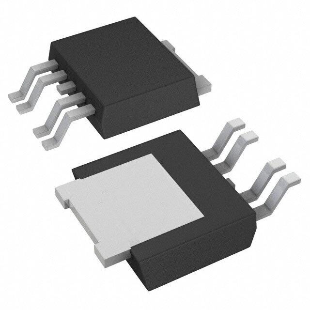
| 产品图片 |
|
| rohs | 符合RoHS无铅 / 符合限制有害物质指令(RoHS)规范要求 |
| 产品系列 | 电源管理 IC,低压差稳压器,Texas Instruments LP2989ILD-5.0/NOPB- |
| 数据手册 | |
| 产品型号 | LP2989ILD-5.0/NOPB |
| PSRR/纹波抑制—典型值 | 60 dB |
| 产品 | Micropower Low-Noise Ultra Low-Dropout Regulator |
| 产品目录页面 | |
| 产品种类 | 低压差稳压器 |
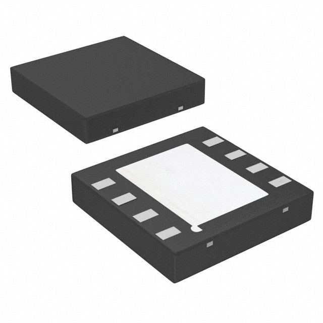
| 供应商器件封装 | 8-WSON (4x4) |
| 其它名称 | *LP2989ILD-5.0/NOPB |
| 包装 | 剪切带 (CT) |
| 商标 | Texas Instruments |
| 回动电压—最大值 | 650 mV |
| 安装类型 | 表面贴装 |
| 安装风格 | SMD/SMT |
| 封装 | Reel |
| 封装/外壳 | 8-WDFN 裸露焊盘 |
| 封装/箱体 | WSON-8 |
| 工作温度 | -40°C ~ 125°C |
| 工厂包装数量 | 1000 |
| 最大工作温度 | + 125 C |
| 最大输入电压 | 16 V |
| 最小工作温度 | - 40 C |
| 最小输入电压 | 2.1 V |
| 标准包装 | 1 |
| 电压-跌落(典型值) | 0.31V @ 500mA |
| 电压-输入 | 最高 16V |
| 电压-输出 | 5V |
| 电流-输出 | 500mA |
| 电流-限制(最小值) | 600mA |
| 稳压器拓扑 | 正,固定式 |
| 稳压器数 | 1 |
| 类型 | Fixed-output voltage Regulator |
| 系列 | LP2989 |
| 线路调整率 | 0.005 % |
| 设计资源 | http://www.digikey.com/product-highlights/cn/zh/texas-instruments-webench-design-center/3176 |
| 负载调节 | 0.4 % |
| 输出电压 | 5 V |
| 输出电压容差 | 3.5 % |
| 输出电流 | 500 mA |
| 输出端数量 | 1 Output |
| 输出类型 | Fixed |


- 商务部:美国ITC正式对集成电路等产品启动337调查
- 曝三星4nm工艺存在良率问题 高通将骁龙8 Gen1或转产台积电
- 太阳诱电将投资9.5亿元在常州建新厂生产MLCC 预计2023年完工
- 英特尔发布欧洲新工厂建设计划 深化IDM 2.0 战略
- 台积电先进制程称霸业界 有大客户加持明年业绩稳了
- 达到5530亿美元!SIA预计今年全球半导体销售额将创下新高
- 英特尔拟将自动驾驶子公司Mobileye上市 估值或超500亿美元
- 三星加码芯片和SET,合并消费电子和移动部门,撤换高东真等 CEO
- 三星电子宣布重大人事变动 还合并消费电子和移动部门
- 海关总署:前11个月进口集成电路产品价值2.52万亿元 增长14.8%


PDF Datasheet 数据手册内容提取
Product Sample & Technical Tools & Support & Folder Buy Documents Software Community LP2989 SNVS083O–FEBRUARY2005–REVISEDMARCH2015 LP2989 Micropower and Low-Noise, 500-mA Ultra Low-Dropout Regulator for Use With Ceramic Output Capacitors 1 Features 3 Description • 2.1-Vto16-VInputVoltageRange The LP2989 is a fixed-output 500-mA precision LDO 1 regulator designed for use with ceramic output • 2.5-Vto5-VFixedOutputVoltageOptions capacitors. • Ultra-LowDropoutVoltage Output noise can be reduced to 18 μV (typical) by • 500-mAContinuousOutputCurrent connecting an external 10-nF capacitor to the bypass • VeryLowOutputNoiseWithExternalCapacitor pin. • <0.8-µAQuiescentCurrentWhenShutdown Using an optimized Vertically Integrated PNP (VIP) • LowGroundPinCurrentatAllLoads process,theLP2989deliverssuperiorperformance: • 0.75%OutputVoltageAccuracy(AGrade) • Dropout Voltage: Typically 310 mV at 500-mA load,and1mVat100-µAload. • HighPeakCurrentCapability(800-mAtypical) • Ground Pin Current: Typically 3 mA at 500-mA • OvertemperatureandOvercurrentProtection load,and110µAat100-µAload. • −40°Cto125°CJunctionTemperatureRange • Sleep Mode: The LP2989 draws less than 0.8-µA quiescent current when SHUTDOWN pin is pulled 2 Applications low. • NotebooksandDesktopPCs • Error Flag: The built-in error flag goes low when • PDAsandPalmtopComputers the output drops approximately 5% below nominal. • WirelessCommunicationPins • Precision Output: Output voltage accuracy is • SMPSPost-Regulators 0.75% (A grade) and 1.25% (standard grade) at roomtemperature. For output voltages < 2 V, see LP2989LV (SNVS086) datasheet. DeviceInformation(1) PARTNUMBER PACKAGE BODYSIZE(NOM) WSON(8) 4.00mmx4.00mm LP2989 SOIC(8) 4.90mmx3.91mm VSSOP(8) 3.00mmx3.00mm (1) For all available packages, see the orderable addendum at theendofthedatasheet. TypicalApplication *Capacitancevaluesshownareminimumrequiredtoassurestability,butmaybeincreasedwithoutlimit.Larger outputcapacitorprovidesimproveddynamicresponse.SeetheOutputCapacitorsection. **Shutdownmustbeactivelyterminated(seetheShutdownInputOperationsection).TietoIN(pin4)ifnotuse. 1 An IMPORTANT NOTICE at the end of this data sheet addresses availability, warranty, changes, use in safety-critical applications, intellectualpropertymattersandotherimportantdisclaimers.PRODUCTIONDATA.
LP2989 SNVS083O–FEBRUARY2005–REVISEDMARCH2015 www.ti.com Table of Contents 1 Features.................................................................. 1 7.3 FeatureDescription.................................................14 2 Applications........................................................... 1 7.4 DeviceFunctionalModes........................................15 3 Description............................................................. 1 8 ApplicationandImplementation........................ 16 4 RevisionHistory..................................................... 2 8.1 ApplicationInformation............................................16 8.2 TypicalApplication .................................................16 5 PinConfigurationandFunctions......................... 3 9 PowerSupplyRecommendations...................... 20 6 Specifications......................................................... 4 10 Layout................................................................... 20 6.1 AbsoluteMaximumRatings......................................4 6.2 ESDRatings..............................................................4 10.1 LayoutGuidelines.................................................20 6.3 RecommendedOperatingConditions.......................5 10.2 LayoutExample....................................................20 6.4 ThermalInformation..................................................5 11 DeviceandDocumentationSupport................. 21 6.5 ElectricalCharacteristics...........................................5 11.1 DocumentationSupport .......................................21 6.6 TypicalCharacteristics..............................................7 11.2 Trademarks...........................................................21 7 DetailedDescription............................................ 14 11.3 ElectrostaticDischargeCaution............................21 7.1 Overview.................................................................14 11.4 Glossary................................................................21 7.2 FunctionalBlockDiagram.......................................14 12 Mechanical,Packaging,andOrderable Information........................................................... 22 4 Revision History ChangesfromRevisionN(December2014)toRevisionO Page • Changed30-Vto16-V ........................................................................................................................................................... 1 • DeletedtrademarksymbolfromVIPwhichisnolongertrademarked .................................................................................. 1 • ChangedpinnamestoTInomenclature;referencestoNationaltoTI;addnotestoTypicalApplicationonfirstpage; fixerrorsinECtablereformat;replaceHandlingRatingswithESDRatings;takeoutOutputVoltageOptionsand addgraphictoMechanicalsection;changedLLPpackagenamereferencestoWSON;addedoverbarto SHUTDOWNpinreferences;fixulinkforLP2989LVreferences........................................................................................... 1 • ChangeddescriptionofN/Cpin;adddescriptionofThermalPad;change"Ground"to"ThermalPad"forNGN drawing .................................................................................................................................................................................. 3 • ChangedreferencetoNationaltoTI ..................................................................................................................................... 4 • Deleted"Operating"rowfromInputsupplyvoltage;thermalvaluesfromfootnote2............................................................ 4 • Changed1.6to16inROCinputsupplyvoltage ................................................................................................................... 5 • Addedword"OFF" ................................................................................................................................................................. 6 • Changed"high"to"low"....................................................................................................................................................... 14 • Changedwordingof"OperationwithShutdownControl"subsection ................................................................................. 15 • ChangedV toV ....................................................................................................................................................... 15 ON/OFF SD • Changed"guaranteed"to"ensured"in"CAUTION"............................................................................................................. 15 • ChangedV toV ....................................................................................................................................................... 15 ON/OFF SD • ChangedwordingoflastsentenceofintroductoryDetailedDesignProcedureparagraph ................................................ 17 • Changedwords"size"and"amount"forcapacitorsto"value" ............................................................................................ 17 • Changedwordingoffirstsentence,secondparagraphofNoiseBypassCapacitorsubsection ......................................... 18 • AddedDocumentationSupportsection ............................................................................................................................... 21 ChangesfromRevisionM(February2005)toRevisionN Page • AddedHandlingRatingtable,FeatureDescriptionsection,DeviceFunctionalModes,Applicationand Implementationsection,PowerSupplyRecommendationssection,Layoutsection,DeviceandDocumentation Supportsection,andMechanical,Packaging,andOrderableInformationsection;addupdatedThermalInformation values .................................................................................................................................................................................... 1 2 SubmitDocumentationFeedback Copyright©2005–2015,TexasInstrumentsIncorporated ProductFolderLinks:LP2989
LP2989 www.ti.com SNVS083O–FEBRUARY2005–REVISEDMARCH2015 5 Pin Configuration and Functions D/DGKPackages 8-PinSOICandVSSOP NGNPackage TopView 8-LeadWSON TopView PinFunctions PIN I/O DESCRIPTION NAME NO. BYPASS 1 I Bypasscapacitorinput ERROR 7 O Errorsignaloutput GROUND 3 — GND INPUT 4 I Regulatorpowerinput DONOTCONNECT.Devicepin2isreservedforpostpackagingtestandcalibrationofthe LP2989V accuracy.Devicepin2mustbeleftfloating.Donotconnecttoanypotential. OUT Donotconnecttoground.Anyattempttodopincontinuitytestingondevicepin2is N/C 2 — discouraged.Continuitytestresultswillbevariabledependingontheactionsofthefactory calibration.Aggressivepincontinuitytesting(highvoltage,orhighcurrent)ondevicepin2 mayactivatethetrimcircuitryforcingV tomoveoutoftolerance. OUT OUTPUT 5 O Regulatedoutputvoltage SENSE 6 I Feedbackvoltagesenseinput SHUTDOWN 8 I Shutdowninput TheexposedthermalpadonthebottomoftheWSONpackageshouldbeconnectedtoa copperthermalpadonthePCBunderthepackage.Theuseofthermalviastoremoveheat fromthepackageintothePCBisrecommended.Connectthethermalpadtoground ThermalPad — — potentialorleavefloating.Donotconnectthethermalpadtoanypotentialotherthanthe samegroundpotentialseenatdevicepin3.ForadditionalinformationonusingTI'sNonPull BackWSONpackage,seeApplicationNoteAN-1187LeadlessLeadframePackage(LLP) (SNOA401). Copyright©2005–2015,TexasInstrumentsIncorporated SubmitDocumentationFeedback 3 ProductFolderLinks:LP2989
LP2989 SNVS083O–FEBRUARY2005–REVISEDMARCH2015 www.ti.com 6 Specifications 6.1 Absolute Maximum Ratings IfMilitary/AerospacespecifieddevicesarerequiredcontacttheTexasInstrumentsSalesOffice/Distributorsforavailabilityand specifications.(1) MIN MAX UNIT Operatingjunctiontemperature –40 125 °C Powerdissipation(2) InternallyLimited Inputsupplyvoltage Survival –0.3 16 V SENSEpin –0.3 6 V Outputvoltage Survival(3) –0.3 16 V I (Survival) Short-circuitprotected OUT Input-outputvoltage Survival(4) –0.3 16 V Storagetemperaturerange,T –65 150 °C stg (1) StressesbeyondthoselistedunderAbsoluteMaximumRatingsmaycausepermanentdamagetothedevice.Thesearestressratings only,whichdonotimplyfunctionaloperationofthedeviceattheseoranyotherconditionsbeyondthoseindicatedunderRecommended OperatingConditions.Exposuretoabsolute-maximum-ratedconditionsforextendedperiodsmayaffectdevicereliability. (2) Themaximumallowablepowerdissipationisafunctionofthemaximumjunctiontemperature,T ),thejunction-to-ambientthermal J(MAX resistance,R ,andtheambienttemperature,T .Themaximumallowablepowerdissipationatanyambienttemperatureiscalculated θJA A using:P =(T –T )/R .ThevalueR fortheWSON(NGN)packageisspecificallydependentonPCBtracearea,trace (MAX) J(MAX) A θJA θJA material,andthenumberoflayersandthermalvias.ForimprovedthermalresistanceandpowerdissipationfortheWSONpackage, refertoApplicationNoteAN-1187LeadlessLeadframePackage(LLP)(SNOA401)..Exceedingthemaximumallowablepower dissipationwillcauseexcessivedietemperature,andtheregulatorwillgointothermalshutdown. (3) Ifusedinadual-supplysystemwheretheregulatorloadisreturnedtoanegativesupply,theLP2989outputmustbediode-clampedto ground. (4) TheoutputPNPstructurecontainsadiodebetweentheINandOUTpinsthatisnormallyreverse-biased.Forcingtheoutputabovethe inputwillturnonthisdiodeandmayinducealatch-upmodewhichcandamagethepart. 6.2 ESD Ratings VALUE UNIT V Electrostaticdischarge Human-bodymodel(HBM),perANSI/ESDA/JEDECJS-001(1) ±2000 V (ESD) (1) JEDECdocumentJEP155statesthat500-VHBMallowssafemanufacturingwithastandardESDcontrolprocess. 4 SubmitDocumentationFeedback Copyright©2005–2015,TexasInstrumentsIncorporated ProductFolderLinks:LP2989
LP2989 www.ti.com SNVS083O–FEBRUARY2005–REVISEDMARCH2015 6.3 Recommended Operating Conditions overoperatingfree-airtemperaturerange(unlessotherwisenoted) MIN MAX UNIT Operatingjunctiontemperature –40 125 °C Operatinginputsupplyvoltage 2.1 16 V 6.4 Thermal Information LP2989 THERMALMETRIC(1) WSON(NGN) SOIC(D) VSSOP(DGK) UNIT 8PINS 8PINS 8PINS R Junction-to-ambientthermalresistance,High-K 34.8 114.5 156.5 θJA R Junction-to-case(top)thermalresistance 28.4 61.1 51.0 θJC(top) R Junction-to-boardthermalresistance 12.0 55.6 76.5 θJB °C/W ψ Junction-to-topcharacterizationparameter 0.2 9.7 4.9 JT ψ Junction-to-boardcharacterizationparameter 12.2 54.9 75.2 JB R Junction-to-case(bottom)thermalresistance 1.3 n/a n/a θJC(bot) (1) Formoreinformationabouttraditionalandnewthermalmetrics,seetheICPackageThermalMetricsapplicationreport,SPRA953. 6.5 Electrical Characteristics Unlessotherwisespecified:T =25°C,V =V +1V,I =1mA,C =4.7µF,C =2.2µF,V =2V. J IN OUT(NOM) OUT OUT IN SD LP2989AI-X.X(1) LP2989I-X.X(1) PARAMETER TESTCONDITIONS UNIT MIN TYP MAX MIN TYP MAX −0.75 0.75 −1.25 1.25 1mA<I <500mA, OUT V +1V≤V ≤16 −1.5 1.5 −2.5 2.5 OUT(NOM) IN V VOUT Outputvoltagetolerance 1mA<IOUT<500mA, %VNOM V +1V≤V ≤16 −4 2.5 −5 3.5 OUT(NOM) IN V,–40°C≤T ≤125°C J 1mA<I <500mA, OUT V +1V≤V ≤16 −3.5 2.5 −4.5 3.5 OUT(NOM) IN V,−25°C≤T ≤125°C J V +1V≤V ≤16 OUT(NOM) IN 0.005 0.014 0.005 0.014 Outputvoltageline V ΔV /ΔV %/V OUT IN regulation V +1V≤V ≤16 OUT(NOM) IN 0.005 0.032 0.005 0.032 V,–40°C≤T ≤125°C J ΔV /ΔI Loadregulation 1mA<I <500mA 0.4 0.4 %V OUT OUT OUT NOM I =100µA 1 3 1 3 OUT I =100µA,–40°C≤T ≤ mV OUT J 1 4 1 4 125°C I =200mA 150 200 150 200 OUT VIN–VOUT Dropoutvoltage(2) IOUT=200mA,–40°C≤TJ 150 300 150 300 mV ≤125°C I =500mA 310 425 310 425 OUT I =500mA,–40°C≤T mV OUT J 310 650 310 650 ≤125°C (1) Limitsare100%productiontestedat25°C.Limitsovertheoperatingtemperaturerangearespecifiedthroughcorrelationusing StatisticalQualityControl(SQC)methods.ThelimitsareusedtocalculateTI’sAverageOutgoingQualityLevel(AOQL). (2) Dropoutvoltageisdefinedastheinputtooutputdifferentialatwhichtheoutputvoltagedrops100mVbelowthevaluemeasuredwitha 1-Vdifferential. Copyright©2005–2015,TexasInstrumentsIncorporated SubmitDocumentationFeedback 5 ProductFolderLinks:LP2989
LP2989 SNVS083O–FEBRUARY2005–REVISEDMARCH2015 www.ti.com Electrical Characteristics (continued) Unlessotherwisespecified:T =25°C,V =V +1V,I =1mA,C =4.7µF,C =2.2µF,V =2V. J IN OUT(NOM) OUT OUT IN SD LP2989AI-X.X(1) LP2989I-X.X(1) PARAMETER TESTCONDITIONS UNIT MIN TYP MAX MIN TYP MAX I =100µA 110 175 110 175 OUT I =100µA,–40°C≤T ≤ µA OUT J 110 200 110 200 125°C I =200mA 1 2 1 2 OUT I =200mA,–40°C≤T mA OUT J 1 3.5 1 3.5 ≤125°C I Groundpincurrent GND I =500mA 3 6 3 6 OUT I =500mA,–40°C≤T mA OUT J 3 9 3 9 ≤125°C V <0.18V,–40°C≤T ≤ SD J 0.5 2 0.5 2 125°C µA V <0.4V 0.05 0.8 0.05 0.8 SD I Peakoutputcurrent V ≥V −5% 600 800 600 800 mA OUT(PK) OUT OUT(NOM) I Shortcircuitcurrent R =0(SteadyState)(3) 1000 1000 mA OUT(MAX) L BW=100Hzto100kHz, Outputnoisevoltage e C =10µF,C = 18 18 µV n (RMS) OUT BYPASS (RMS) .01µF,V =2.5V OUT ΔV /ΔV RippleRejection f=1kHz,C =10µF 60 60 dB OUT IN OUT ΔV /ΔT Outputvoltage See(4),–40°C≤T ≤125°C 20 20 ppm/°C OUT D temperaturecoefficient J SHUTDOWNINPUT V =OutputON 1.4 1.4 H V =OutputON,–40°C≤T H J 1.6 1.6 ≤125°C V SDInputvoltage V SD V =OutputOFF 0.5 0.5 L V =OutputOFF,I ≤2µA, L IN 0.18 0.18 –40°C≤T ≤125°C J V =0 0.001 0.001 SD V =0,–40°C≤T ≤ SD J −1 −1 125°C I SDInputcurrent µA SD V =5V 5 5 SD V =5V,–40°C≤T ≤ SD J 15 15 125°C ERRORCOMPARATOR V =16V 0.001 1 0.001 1 OH IOH Output“HIGH”leakage VOH=16V,–40°C≤TJ≤ 0.001 2 0.001 2 µA 125°C V =V −0.5V, IN OUT(NOM) 150 220 150 220 I =150µA OUT(COMP) VOL Output“LOW”voltage VIN=VOUT(NOM)−0.5V, mV I =150µA,–40°C 150 350 150 350 OUT(COMP) ≤T ≤125°C J −6 −4.8 −3.5 −6 −4.8 −3.5 V Upperthresholdvoltage %V THR(MAX) OUT –40°C≤T ≤125°C −8.3 −4.8 −2.5 −8.3 −4.8 −2.5 J −8.9 −6.6 −4.9 −8.9 −6.6 −4.9 V Lowerthresholdvoltage THR(MIN) –40°C≤T ≤125°C −13 −6.6 −3 −13 −6.6 −3 %V J OUT HYST Hysteresis 2 (3) SeetheTypicalCharacteristicssection. (4) Temperaturecoefficientisdefinedasthemaximum(worst-case)changedividedbythetotaltemperaturerange. 6 SubmitDocumentationFeedback Copyright©2005–2015,TexasInstrumentsIncorporated ProductFolderLinks:LP2989
LP2989 www.ti.com SNVS083O–FEBRUARY2005–REVISEDMARCH2015 6.6 Typical Characteristics T =25°C,C =4.7µF,C =2.2µF,SDistiedtoV ,V =V +1V,I =1mA,V =2.5V(unlessotherwise A OUT IN IN IN OUT(NOM) OUT OUT specified) Figure1.DropoutCharacteristics Figure2.DropoutVoltagevsTemperature Figure4.GNDPinCurrentvsTemperatureandLoad Figure3.DropoutVoltagevsLoadCurrent Figure5.GroundPinCurrentvsLoadCurrent Figure6.InputCurrentvsV IN Copyright©2005–2015,TexasInstrumentsIncorporated SubmitDocumentationFeedback 7 ProductFolderLinks:LP2989
LP2989 SNVS083O–FEBRUARY2005–REVISEDMARCH2015 www.ti.com Typical Characteristics (continued) T =25°C,C =4.7µF,C =2.2µF,SDistiedtoV ,V =V +1V,I =1mA,V =2.5V(unlessotherwise A OUT IN IN IN OUT(NOM) OUT OUT specified) Figure7.InputCurrentvsV Figure8.InputCurrentvsV IN IN Figure9.LineTransientResponse Figure10.LineTransientResponse Figure11.LineTransientResponse Figure12.LineTransientResponse 8 SubmitDocumentationFeedback Copyright©2005–2015,TexasInstrumentsIncorporated ProductFolderLinks:LP2989
LP2989 www.ti.com SNVS083O–FEBRUARY2005–REVISEDMARCH2015 Typical Characteristics (continued) T =25°C,C =4.7µF,C =2.2µF,SDistiedtoV ,V =V +1V,I =1mA,V =2.5V(unlessotherwise A OUT IN IN IN OUT(NOM) OUT OUT specified) Figure13.LoadTransientResponse Figure14.LoadTransientResponse Figure15.ShortCircuitCurrent Figure16.ShortCircuitCurrentvsTemperature Figure17.ShortCircuitCurrent Figure18.ShortCircuitCurrentvsV OUT Copyright©2005–2015,TexasInstrumentsIncorporated SubmitDocumentationFeedback 9 ProductFolderLinks:LP2989
LP2989 SNVS083O–FEBRUARY2005–REVISEDMARCH2015 www.ti.com Typical Characteristics (continued) T =25°C,C =4.7µF,C =2.2µF,SDistiedtoV ,V =V +1V,I =1mA,V =2.5V(unlessotherwise A OUT IN IN IN OUT(NOM) OUT OUT specified) Figure19.RippleRejection Figure20.RippleRejection Figure21.RippleRejection Figure22.RippleRejection Figure23.RippleRejection Figure24.RippleRejection 10 SubmitDocumentationFeedback Copyright©2005–2015,TexasInstrumentsIncorporated ProductFolderLinks:LP2989
LP2989 www.ti.com SNVS083O–FEBRUARY2005–REVISEDMARCH2015 Typical Characteristics (continued) T =25°C,C =4.7µF,C =2.2µF,SDistiedtoV ,V =V +1V,I =1mA,V =2.5V(unlessotherwise A OUT IN IN IN OUT(NOM) OUT OUT specified) Figure25.RippleRejection Figure26.RippleRejectioninDropout Figure27.RippleRejectionvsLoad Figure28.OutputNoiseDensity Figure29.OutputNoiseDensity Figure30.Turn-ONWaveform Copyright©2005–2015,TexasInstrumentsIncorporated SubmitDocumentationFeedback 11 ProductFolderLinks:LP2989
LP2989 SNVS083O–FEBRUARY2005–REVISEDMARCH2015 www.ti.com Typical Characteristics (continued) T =25°C,C =4.7µF,C =2.2µF,SDistiedtoV ,V =V +1V,I =1mA,V =2.5V(unlessotherwise A OUT IN IN IN OUT(NOM) OUT OUT specified) Figure31.Turn-ONWaveform Figure32.Turn-ONWaveform Figure33.Turn-ONWaveform Figure34.I vsShutdown GND Figure35.I vsShutdown Figure36.I vsShutdown GND GND 12 SubmitDocumentationFeedback Copyright©2005–2015,TexasInstrumentsIncorporated ProductFolderLinks:LP2989
LP2989 www.ti.com SNVS083O–FEBRUARY2005–REVISEDMARCH2015 Typical Characteristics (continued) T =25°C,C =4.7µF,C =2.2µF,SDistiedtoV ,V =V +1V,I =1mA,V =2.5V(unlessotherwise A OUT IN IN IN OUT(NOM) OUT OUT specified) Figure37.I vsShutdown Figure38.V vsShutdown GND OUT Figure39.TypicalTemperaturevsV (LP2989-2.5) OUT Copyright©2005–2015,TexasInstrumentsIncorporated SubmitDocumentationFeedback 13 ProductFolderLinks:LP2989
LP2989 SNVS083O–FEBRUARY2005–REVISEDMARCH2015 www.ti.com 7 Detailed Description 7.1 Overview The LP2989 device is a very high-accuracy micro-power voltage regulator with low quiescent current (75 μA typical) and low dropout voltage (typical 40 mV at light loads and 380 mV at 100 mA). It is ideally suited for use inbattery-poweredsystems.TheLP2989blockdiagramcontainsseveralfeatures,including: • Veryhigh-accuracy1.23-Vreference • Fixed2.5-Vto5-Vversions • Shutdowninput • Errorflagoutput • Internalprotectioncircuitry,suchasfoldbackcurrentlimit,andthermalshutdown 7.2 Functional Block Diagram 7.3 Feature Description 7.3.1 High-AccuracyOutputVoltage With special careful design to minimize all contributions to the output voltage error, the LP2989 distinguishes itself as a very high output-voltage-accuracy micro-power LDO. This includes a tight initial tolerance (.75% typical, A grade), extremely good line regulation (.005%/V typical), and a very low output-noise voltage (10 µ VRMS typical),makingthedeviceanidealalow-powervoltagereference. 7.3.2 SleepMode When pulling SHUTDOWN pin to low levels, the LP2989 enters shutdown mode, and a very low quiescent current is consumed. This function is designed for applications which needs a shutdown mode to effectively enhancebatterylifecycle. 7.3.3 ErrorDetectionComparatorOutput The LP2989 will generate a logic low output whenever its output falls out of regulation by more than approximately5%.RefertoApplicationandImplementationformoredetails. 14 SubmitDocumentationFeedback Copyright©2005–2015,TexasInstrumentsIncorporated ProductFolderLinks:LP2989
LP2989 www.ti.com SNVS083O–FEBRUARY2005–REVISEDMARCH2015 Feature Description (continued) 7.3.4 ShortCircuitProtection(CurrentLimit) TheinternalcurrentlimitcircuitisusedtoprotecttheLDOagainsthigh-loadcurrentfaultsorshortingevents.The LDO is not designed to operate in a steady-state current limit. During a current-limit event, the LDO sources constant current. Therefore, the output voltage falls when load impedance decreases. Note also that if a current limit occurs and the resulting output voltage is low, excessive power may be dissipated across the LDO, resulting inathermalshutdownoftheoutput.Afoldbackfeaturelimitstheshort-circuitcurrenttoprotecttheregulatorfrom damage under all load conditions. If OUT is forced below 0 V before EN goes high and the load current required exceedsthefoldbackcurrentlimit,thedevicemaynotstartcorrectly. 7.3.5 ThermalProtection The device contains a thermal shutdown protection circuit to turn off the output current when excessive heat is dissipated in the LDO. The thermal time-constant of the semiconductor die is fairly short, and thus the output cycles on and off at a high rate when thermal shutdown is reached until the power dissipation is reduced. The internal protection circuitry of the device is designed to protect against thermal overload conditions. The circuitry is not intended to replace proper heat sinking. Continuously running the device into thermal shutdown degrades itsreliability. 7.4 Device Functional Modes 7.4.1 OperationWith16V≥ V > V +1V IN OUT(TARGET) The device operates if the input voltage is equal to, or exceeds V + 1 V. At input voltages below the OUT(TARGET) minimumV requirement,thedevicesdoesnotoperatecorrectly,andoutputvoltagemaynotreachtargetvalue. IN 7.4.2 OperationwithShutdownControl If the voltage on the SHUTDOWN pin is less than 0.18 V, the output is ensured to be OFF. When the voltage on the SHUTDOWN pin is more than 1.6 V the output is ensured to be ON. Operating with the SHUTDOWN pin voltagebetween0.18Vand1.6Visstronglydiscouragedasthestatusoftheoutputisnotensured. 7.4.3 ShutdownInputOperation The LP2989 is shut off by driving the SHUTDOWN pin low, and turned on by pulling it high. If this feature is not tobeused,the SHUTDOWNshouldbetiedtoV tokeeptheregulatoroutputonatalltimes. IN Toassureproperoperation,thesignalsourceusedtodrivetheShutdowninputmustbeabletoswingaboveand belowthespecifiedturn-on/turn-offvoltagethresholdslistedintheElectricalCharacteristics sectionunderV . SD To prevent mis-operation, the turn-on (and turn-off) voltage signals applied to the Shutdown input must have a slewratewhichis≥ 40mV/µs. CAUTION The regulator output voltage cannot be ensured if a slow-moving AC (or DC) signal is applied that is in the range between the specified turn-on and turn-off voltages listed undertheelectricalspecificationV (seetheElectricalCharacteristicstable). SD Copyright©2005–2015,TexasInstrumentsIncorporated SubmitDocumentationFeedback 15 ProductFolderLinks:LP2989
LP2989 SNVS083O–FEBRUARY2005–REVISEDMARCH2015 www.ti.com 8 Application and Implementation NOTE Information in the following applications sections is not part of the TI component specification, and TI does not warrant its accuracy or completeness. TI’s customers are responsible for determining suitability of components for their purposes. Customers should validateandtesttheirdesignimplementationtoconfirmsystemfunctionality. 8.1 Application Information The LP2989 is a linear voltage regulator operating from 2.1 V to 16 V on the input and regulates voltages between 2.5 V to 5 V with 0.75% accuracy and 500 mA maximum outputs current. Efficiency is defined by the ratio of output voltage to input voltage because the LP2989 is a linear voltage regulator. To achieve high efficiency, the dropout voltage (V – V ) must be as small as possible, thus requiring a very low dropout LDO. IN OUT Successfully implementing an LDO in an application depends on the application requirements. If the requirements are simply input voltage and output voltage, compliance specifications (such as internal power dissipation or stability) must be verified to ensure a solid design. If timing, start-up, noise, PSRR, or any other transient specification is required, the design becomes more challenging. This section discusses the implementationandbehavioroftheLP2989LDO. 8.2 Typical Application *Capacitancevaluesshownareminimumrequiredtoassurestability,butmaybeincreasedwithoutlimit.Larger outputcapacitorprovidesimproveddynamicresponse.SeetheOutputCapacitorsection. **Shutdownmustbeactivelyterminated(seetheShutdownInputOperationsection).TietoIN(pin4)ifnotuse. Figure40. TypicalApplicationSchematic 8.2.1 DesignRequirements DESIGNPARAMETER DESIGNREQUIREMENT Inputvoltage 6.5V,±10%, Outputvoltage 5V,±1% Outputcurrent 500mA(maximum),1mA(minimum) RMSnoise,100Hzto100kHz 18μV typical RMS PSRRat1kHz 60dBtypical 16 SubmitDocumentationFeedback Copyright©2005–2015,TexasInstrumentsIncorporated ProductFolderLinks:LP2989
LP2989 www.ti.com SNVS083O–FEBRUARY2005–REVISEDMARCH2015 8.2.2 DetailedDesignProcedure At 500-mA loading, the dropout of the LP2989 has 650-mV maximum dropout over temperature, thus an 1500- mV headroom is sufficient for operation over both input and output voltage accuracy. The efficiency of the LP2989 in this configuration is V / V = 76.9%. To achieve the smallest form factor, the WSON package is OUT IN selected. Input and output capacitors are selected in accordance with the capacitor recommendations. Ceramic capacitances of 2.2 μF for the input and one 4.7-μF capacitor for the output are selected. With an efficiency of 76.9% and a 500-mA maximum load, the internal power dissipation is 750 mW, which corresponds to a 26.1°C junction temperature rise for the WSON package. With an 85°C maximum ambient temperature, the junction temperature is at 111.1°C. To minimize noise, a bypass capacitance (C ) of 0.01 µF is placed from the BYPASS BYPASSpin(devicepin1)todeviceground(devicepin3). 8.2.2.1 WSONPackageDevices The LP2989 is offered in the 8-lead WSON surface mount package to allow for increased power dissipation compared to the SOIC and VSSOP packages. For details on thermal performance as well as mounting and solderingspecifications,refertoApplicationNoteAN-1187 LeadlessLeadframePackage(LLP)(SNOA401). Foroutputvoltages<2V,seeLP2989LV(SNVS086)datasheet. 8.2.2.2 ExternalCapacitors Like any low-dropout regulator, the LP2989 requires external capacitors for regulator stability. These capacitors mustbecorrectlyselectedforgoodperformance. 8.2.2.2.1 InputCapacitor An input capacitor whose value is at least 2.2 µF is required between the LP2989 input and ground (the amount ofcapacitancemaybeincreasedwithoutlimit). Characterization testing performed on the LP2989 has shown that if the value of actual input capacitance drops below about 1.5 µF, an unstable operating condition may result. Therefore, the next larger standard size (2.2 µF) is specified as the minimum required input capacitance. Capacitor tolerance and temperature variation must be considered when selecting a capacitor (see Capacitor Characteristics section) to assure the minimum requirementof1.5µFismetoveralloperatingconditions. The input capacitor must be located at a distance of not more than 0.5 inches from the input pin and returned to a clean analog ground. Any good quality ceramic or tantalum may be used for this capacitor, assuming the minimumcapacitancerequirementismet. 8.2.2.2.2 OutputCapacitor The LP2989 requires a ceramic output capacitor whose value is at least 4.7 µF. The actual amount of capacitance on the output must never drop below about 3.5 µF or unstable operation may result. For this reason, capacitancetoleranceandtemperaturecharacteristicsmustbeconsideredwhenselectinganoutputcapacitor. The LP2989 is designed specifically to work with ceramic output capacitors, using circuitry which allows the regulator to be stable across the entire range of output current with an output capacitor whose ESR is as low as 4 mΩ. It may also be possible to use Tantalum or film capacitors at the output, but these are not as attractive for reasonsofsizeandcost(seetheCapacitorCharacteristicssection). The output capacitor must meet the requirement for minimum amount of capacitance and also have an equivalent series resistance (ESR) value which is within the stable range. Curves are provided which show the stableESRrangeasafunctionofloadcurrent(seeFigure41). Copyright©2005–2015,TexasInstrumentsIncorporated SubmitDocumentationFeedback 17 ProductFolderLinks:LP2989
LP2989 SNVS083O–FEBRUARY2005–REVISEDMARCH2015 www.ti.com Figure41. StableRegionforOutputCapacitorESR NOTE Important: The output capacitor must maintain its ESR within the stable region over the fulloperatingtemperaturerangeoftheapplicationtoassurestability. It is important to remember that capacitor tolerance and variation with temperature must be considered when selectinganoutputcapacitorsothattheminimumrequiredamountofoutputcapacitanceisprovidedoverthefull operatingtemperaturerange.(SeetheCapacitorCharacteristics section.) The output capacitor must be located not more than 0.5 inches from the OUT pin and returned to a clean analog ground. 8.2.2.2.3 NoiseBypassCapacitor Connecting a 10-nF capacitor to the BYPASS pin significantly reduces noise on the regulator output. However, thecapacitorisconnecteddirectlytoahigh-impedancecircuitinthebandgapreference. Because this circuit has only a few microamperes flowing in it, any significant loading on this node will cause the regulated output voltage to drop. For this reason, DC leakage current through the noise bypass capacitor must neverexceed100nA,andshouldbekeptaslowaspossibleforbestoutputvoltageaccuracy. The types of capacitors best suited for the noise bypass capacitor are ceramic and film. High-quality ceramic capacitors with either NPO or COG dielectric typically have very low leakage. Ten-nF polypropolene and polycarbonate film capacitors are available in small surface-mount packages and typically have extremely low leakagecurrent. 8.2.2.3 CapacitorCharacteristics 8.2.2.3.1 Ceramic The LP2989 was designed to work with ceramic capacitors on the output to take advantage of the benefits they offer:forcapacitancevaluesinthe4.7 µFrange,ceramicsaretheleastexpensiveandalsohavethelowestESR values (which makes them best for eliminating high-frequency noise). The ESR of a typical 4.7-µF ceramic capacitor is in the range of 10 mΩ to 15 mΩ, which easily meets the ESR limits required for stability by the LP2989. One disadvantage of ceramic capacitors is that their capacitance can vary with temperature. Many large-value ceramic capacitors (≥ 2.2 µF) are manufactured with the Z5U or Y5V temperature characteristic, which results in thecapacitancedroppingbymorethan50%asthetemperaturegoesfrom25°Cto85°C. This could cause problems if a 4.7-µF capacitor were used on the output because it will drop down to approximately 2.4 µF at high ambient temperatures (which could cause the LP2989 to oscillate). Another significant problem with Z5U and Y5V dielectric devices is that the capacitance drops severely with applied voltage. A typical Z5U or Y5V capacitor can lose 60% of its rated capacitance with half of the rated voltage appliedtoit. 18 SubmitDocumentationFeedback Copyright©2005–2015,TexasInstrumentsIncorporated ProductFolderLinks:LP2989
LP2989 www.ti.com SNVS083O–FEBRUARY2005–REVISEDMARCH2015 Forthesereasons,X7RandX5RtypeceramiccapacitorsmustbeusedontheinputandoutputoftheLP2989. 8.2.2.3.2 Tantalum Tantalum capacitors are less desirable than ceramics for use as output capacitors because they are typically moreexpensivewhencomparingequivalentcapacitanceandvoltageratingsinthe1µFto4.7 µFrange. Another important consideration is that Tantalum capacitors have higher ESR values than equivalent size ceramics; while it may be possible to find a Tantalum capacitor with an ESR value within the stable range, it would have to be larger in capacitance (which means bigger and more costly) than a ceramic capacitor with the sameESRvalue. It should also be noted that the ESR of a typical Tantalum will increase about 2:1 as the temperature goes from 25°Cdownto−40°C,sosomeguardbandmustbeallowed. Tantalumcapacitorsmaybeusedontheinputaslongastherequirementforminimumcapacitanceismet. 8.2.2.3.3 Film Polycarbonateandpolypropelenefilmcapacitorshaveexcellentelectricalperformance:theirESRisthelowestof thethreetypeslisted,theircapacitanceisverystablewithtemperature,andDCleakagecurrentisextremelylow. One disadvantage is that film capacitors are larger in physical size than ceramic or tantalum which makes film a poorchoiceforeitherinputoroutputcapacitors. However, their low leakage makes them a good choice for the noise bypass capacitor. Because the required amountofcapacitanceisonly0.01µF,smallsurface-mountfilmcapacitorsareavailableinthissize. 8.2.2.4 ReverseInput-OutputVoltage The PNP power transistor used as the pass element in the LP2989 has an inherent diode connected between theregulatoroutputandinput. Duringnormaloperation(wheretheinputvoltageishigherthantheoutput)thisdiodeisreverse-biased. However, if the output is pulled above the input, this diode will turn on and current will flow into the regulator output. Insuchcases,aparasiticSCRcanlatchwhichwillallowhighcurrenttoflowintoV candamagethepart. IN In any application where the output may be pulled above the input, an external Schottky diode must be connected from V to V (cathode on V , anode on V ), to limit the reverse voltage across the LP2989 to IN OUT IN OUT 0.3V(seetheAbsoluteMaximumRatingstable). 8.2.3 ApplicationCurves Figure42.LineTransientResponse Figure43.LoadTransientResponse Copyright©2005–2015,TexasInstrumentsIncorporated SubmitDocumentationFeedback 19 ProductFolderLinks:LP2989
LP2989 SNVS083O–FEBRUARY2005–REVISEDMARCH2015 www.ti.com 9 Power Supply Recommendations The LP2989 is designed to operate from an input voltage supply range from 2.1 V to 16 V. The input voltage range provides adequate headroom for the device to have a regulated output. This input supply must be well regulated. If the input supply is noisy, additional input capacitors with low ESR can help improve the output noise performance. 10 Layout 10.1 Layout Guidelines For best overall performance, place all circuit components on the same side of the circuit board and as near as practical to the respective LDO pin connections. Place ground return connections to the input and output capacitor, and to the LDO ground pin as close to each other as possible, connected by a wide, component-side, copper surface. The use of vias and long traces to create LDO circuit connections is strongly discouraged and negatively affects system performance. This grounding and layout scheme minimizes inductive parasitics, and thereby reduces load-current transients, minimizes noise, and increases circuit stability. A ground reference plane is also recommended and is either embedded in the PCB itself or located on the bottom side of the PCB opposite the components. This reference plane serves to assure accuracy of the output voltage, shield noise, and behaves similar to a thermal plane to spread (or sink) heat from the LDO device. In most applications, this groundplaneisnecessarytomeetthermalrequirements. 10.2 Layout Example BYPASS SHUTDOWN Error Pullup Resistor N/C ERROR VOUT Ground GROUND SENSE Input Capacitor VOUT IN OUT VIN Output Capacitor Figure44. LayoutExample 20 SubmitDocumentationFeedback Copyright©2005–2015,TexasInstrumentsIncorporated ProductFolderLinks:LP2989
LP2989 www.ti.com SNVS083O–FEBRUARY2005–REVISEDMARCH2015 11 Device and Documentation Support 11.1 Documentation Support 11.1.1 RelatedDocumentation Forrelateddocumentationseethefollowing: LP2989LV(SNVS086)datasheet ApplicationNoteAN-1187LeadlessLeadframePackage(LLP)(SNOA401). 11.2 Trademarks Alltrademarksarethepropertyoftheirrespectiveowners. 11.3 Electrostatic Discharge Caution Thesedeviceshavelimitedbuilt-inESDprotection.Theleadsshouldbeshortedtogetherorthedeviceplacedinconductivefoam duringstorageorhandlingtopreventelectrostaticdamagetotheMOSgates. 11.4 Glossary SLYZ022—TIGlossary. Thisglossarylistsandexplainsterms,acronyms,anddefinitions. Copyright©2005–2015,TexasInstrumentsIncorporated SubmitDocumentationFeedback 21 ProductFolderLinks:LP2989
LP2989 SNVS083O–FEBRUARY2005–REVISEDMARCH2015 www.ti.com 12 Mechanical, Packaging, and Orderable Information The following pages include mechanical, packaging, and orderable information. This information is the most current data available for the designated devices. This data is subject to change without notice and revision of thisdocument.Forbrowser-basedversionsofthisdatasheet,refertotheleft-handnavigation. Figure45. POAOrderableDeviceKey 22 SubmitDocumentationFeedback Copyright©2005–2015,TexasInstrumentsIncorporated ProductFolderLinks:LP2989
PACKAGE OPTION ADDENDUM www.ti.com 6-Nov-2018 PACKAGING INFORMATION Orderable Device Status Package Type Package Pins Package Eco Plan Lead/Ball Finish MSL Peak Temp Op Temp (°C) Device Marking Samples (1) Drawing Qty (2) (6) (3) (4/5) LP2989AILD-3.0/NOPB ACTIVE WSON NGN 8 1000 Green (RoHS CU SN Level-3-260C-168 HR -40 to 125 L01HA & no Sb/Br) LP2989AILD-3.3/NOPB ACTIVE WSON NGN 8 1000 Green (RoHS CU SN Level-3-260C-168 HR -40 to 125 L01JA & no Sb/Br) LP2989AILD-5.0/NOPB ACTIVE WSON NGN 8 1000 Green (RoHS CU SN Level-3-260C-168 HR -40 to 125 L01KA & no Sb/Br) LP2989AILDX-2.8/NOPB ACTIVE WSON NGN 8 4500 Green (RoHS CU SN Level-3-260C-168 HR -40 to 125 L000A & no Sb/Br) LP2989AIM-2.5/NOPB ACTIVE SOIC D 8 95 Green (RoHS CU SN Level-1-260C-UNLIM -40 to 125 2989A & no Sb/Br) IM2.5 LP2989AIM-3.0/NOPB ACTIVE SOIC D 8 95 Green (RoHS CU SN Level-1-260C-UNLIM -40 to 125 2989A & no Sb/Br) IM3.0 LP2989AIM-3.3/NOPB ACTIVE SOIC D 8 95 Green (RoHS CU SN Level-1-260C-UNLIM -40 to 125 2989A & no Sb/Br) IM3.3 LP2989AIM-5.0 NRND SOIC D 8 95 TBD Call TI Call TI -40 to 125 2989A IM5.0 LP2989AIM-5.0/NOPB ACTIVE SOIC D 8 95 Green (RoHS CU SN Level-1-260C-UNLIM -40 to 125 2989A & no Sb/Br) IM5.0 LP2989AIMM-2.5/NOPB ACTIVE VSSOP DGK 8 1000 Green (RoHS CU SN Level-1-260C-UNLIM -40 to 125 LA0A & no Sb/Br) LP2989AIMM-3.0/NOPB ACTIVE VSSOP DGK 8 1000 Green (RoHS CU SN Level-1-260C-UNLIM -40 to 125 LA1A & no Sb/Br) LP2989AIMM-3.3/NOPB ACTIVE VSSOP DGK 8 1000 Green (RoHS CU SN Level-1-260C-UNLIM -40 to 125 LA2A & no Sb/Br) LP2989AIMM-5.0/NOPB ACTIVE VSSOP DGK 8 1000 Green (RoHS CU SN Level-1-260C-UNLIM -40 to 125 LA4A & no Sb/Br) LP2989AIMMX-2.5/NOPB ACTIVE VSSOP DGK 8 3500 Green (RoHS CU SN Level-1-260C-UNLIM -40 to 125 LA0A & no Sb/Br) LP2989AIMMX-5.0/NOPB ACTIVE VSSOP DGK 8 3500 Green (RoHS CU SN Level-1-260C-UNLIM -40 to 125 LA4A & no Sb/Br) LP2989AIMX-2.5/NOPB ACTIVE SOIC D 8 2500 Green (RoHS CU SN Level-1-260C-UNLIM -40 to 125 2989A & no Sb/Br) IM2.5 LP2989AIMX-3.0/NOPB ACTIVE SOIC D 8 2500 Green (RoHS CU SN Level-1-260C-UNLIM -40 to 125 2989A & no Sb/Br) IM3.0 Addendum-Page 1
PACKAGE OPTION ADDENDUM www.ti.com 6-Nov-2018 Orderable Device Status Package Type Package Pins Package Eco Plan Lead/Ball Finish MSL Peak Temp Op Temp (°C) Device Marking Samples (1) Drawing Qty (2) (6) (3) (4/5) LP2989AIMX-3.3/NOPB ACTIVE SOIC D 8 2500 Green (RoHS CU SN Level-1-260C-UNLIM -40 to 125 2989A & no Sb/Br) IM3.3 LP2989AIMX-5.0/NOPB ACTIVE SOIC D 8 2500 Green (RoHS CU SN Level-1-260C-UNLIM -40 to 125 2989A & no Sb/Br) IM5.0 LP2989ILD-2.5/NOPB ACTIVE WSON NGN 8 1000 Green (RoHS CU SN Level-3-260C-168 HR -40 to 125 L01FA & no Sb/Br) B LP2989ILD-3.0/NOPB ACTIVE WSON NGN 8 1000 Green (RoHS CU SN Level-3-260C-168 HR -40 to 125 L01HA & no Sb/Br) B LP2989ILD-3.3/NOPB ACTIVE WSON NGN 8 1000 Green (RoHS CU SN Level-3-260C-168 HR -40 to 125 L01JA & no Sb/Br) B LP2989ILD-5.0/NOPB ACTIVE WSON NGN 8 1000 Green (RoHS CU SN Level-3-260C-168 HR -40 to 125 L01KA & no Sb/Br) B LP2989ILDX-3.3/NOPB ACTIVE WSON NGN 8 4500 Green (RoHS CU SN Level-3-260C-168 HR -40 to 125 L01JA & no Sb/Br) B LP2989ILDX-5.0/NOPB ACTIVE WSON NGN 8 4500 Green (RoHS CU SN Level-3-260C-168 HR -40 to 125 L01KA & no Sb/Br) B LP2989IM-2.5/NOPB ACTIVE SOIC D 8 95 Green (RoHS CU SN Level-1-260C-UNLIM -40 to 125 2989 & no Sb/Br) IM2.5 LP2989IM-3.0/NOPB ACTIVE SOIC D 8 95 Green (RoHS CU SN Level-1-260C-UNLIM -40 to 125 2989 & no Sb/Br) IM3.0 LP2989IM-3.3 NRND SOIC D 8 95 TBD Call TI Call TI -40 to 125 2989 IM3.3 LP2989IM-3.3/NOPB ACTIVE SOIC D 8 95 Green (RoHS CU SN Level-1-260C-UNLIM -40 to 125 2989 & no Sb/Br) IM3.3 LP2989IM-5.0/NOPB ACTIVE SOIC D 8 95 Green (RoHS CU SN Level-1-260C-UNLIM -40 to 125 2989 & no Sb/Br) IM5.0 LP2989IMM-2.8/NOPB ACTIVE VSSOP DGK 8 1000 Green (RoHS CU SN Level-1-260C-UNLIM -40 to 125 LA6B & no Sb/Br) LP2989IMM-3.0/NOPB ACTIVE VSSOP DGK 8 1000 Green (RoHS CU SN Level-1-260C-UNLIM -40 to 125 LA1B & no Sb/Br) LP2989IMM-3.3/NOPB ACTIVE VSSOP DGK 8 1000 Green (RoHS CU SN Level-1-260C-UNLIM -40 to 125 LA2B & no Sb/Br) LP2989IMM-5.0/NOPB ACTIVE VSSOP DGK 8 1000 Green (RoHS CU SN Level-1-260C-UNLIM -40 to 125 LA4B & no Sb/Br) LP2989IMMX-2.8/NOPB ACTIVE VSSOP DGK 8 3500 Green (RoHS CU SN Level-1-260C-UNLIM -40 to 125 LA6B & no Sb/Br) Addendum-Page 2
PACKAGE OPTION ADDENDUM www.ti.com 6-Nov-2018 Orderable Device Status Package Type Package Pins Package Eco Plan Lead/Ball Finish MSL Peak Temp Op Temp (°C) Device Marking Samples (1) Drawing Qty (2) (6) (3) (4/5) LP2989IMMX-5.0 NRND VSSOP DGK 8 3500 TBD Call TI Call TI -40 to 125 LA4B LP2989IMMX-5.0/NOPB ACTIVE VSSOP DGK 8 3500 Green (RoHS CU SN Level-1-260C-UNLIM -40 to 125 LA4B & no Sb/Br) LP2989IMX-2.5/NOPB ACTIVE SOIC D 8 2500 Green (RoHS CU SN Level-1-260C-UNLIM -40 to 125 2989 & no Sb/Br) IM2.5 LP2989IMX-3.3/NOPB ACTIVE SOIC D 8 2500 Green (RoHS CU SN Level-1-260C-UNLIM -40 to 125 2989 & no Sb/Br) IM3.3 LP2989IMX-5.0/NOPB ACTIVE SOIC D 8 2500 Green (RoHS CU SN Level-1-260C-UNLIM -40 to 125 2989 & no Sb/Br) IM5.0 (1) The marketing status values are defined as follows: ACTIVE: Product device recommended for new designs. LIFEBUY: TI has announced that the device will be discontinued, and a lifetime-buy period is in effect. NRND: Not recommended for new designs. Device is in production to support existing customers, but TI does not recommend using this part in a new design. PREVIEW: Device has been announced but is not in production. Samples may or may not be available. OBSOLETE: TI has discontinued the production of the device. (2) RoHS: TI defines "RoHS" to mean semiconductor products that are compliant with the current EU RoHS requirements for all 10 RoHS substances, including the requirement that RoHS substance do not exceed 0.1% by weight in homogeneous materials. Where designed to be soldered at high temperatures, "RoHS" products are suitable for use in specified lead-free processes. TI may reference these types of products as "Pb-Free". RoHS Exempt: TI defines "RoHS Exempt" to mean products that contain lead but are compliant with EU RoHS pursuant to a specific EU RoHS exemption. Green: TI defines "Green" to mean the content of Chlorine (Cl) and Bromine (Br) based flame retardants meet JS709B low halogen requirements of <=1000ppm threshold. Antimony trioxide based flame retardants must also meet the <=1000ppm threshold requirement. (3) MSL, Peak Temp. - The Moisture Sensitivity Level rating according to the JEDEC industry standard classifications, and peak solder temperature. (4) There may be additional marking, which relates to the logo, the lot trace code information, or the environmental category on the device. (5) Multiple Device Markings will be inside parentheses. Only one Device Marking contained in parentheses and separated by a "~" will appear on a device. If a line is indented then it is a continuation of the previous line and the two combined represent the entire Device Marking for that device. (6) Lead/Ball Finish - Orderable Devices may have multiple material finish options. Finish options are separated by a vertical ruled line. Lead/Ball Finish values may wrap to two lines if the finish value exceeds the maximum column width. Important Information and Disclaimer:The information provided on this page represents TI's knowledge and belief as of the date that it is provided. TI bases its knowledge and belief on information provided by third parties, and makes no representation or warranty as to the accuracy of such information. Efforts are underway to better integrate information from third parties. TI has taken and Addendum-Page 3
PACKAGE OPTION ADDENDUM www.ti.com 6-Nov-2018 continues to take reasonable steps to provide representative and accurate information but may not have conducted destructive testing or chemical analysis on incoming materials and chemicals. TI and TI suppliers consider certain information to be proprietary, and thus CAS numbers and other limited information may not be available for release. In no event shall TI's liability arising out of such information exceed the total purchase price of the TI part(s) at issue in this document sold by TI to Customer on an annual basis. Addendum-Page 4
PACKAGE MATERIALS INFORMATION www.ti.com 15-Sep-2018 TAPE AND REEL INFORMATION *Alldimensionsarenominal Device Package Package Pins SPQ Reel Reel A0 B0 K0 P1 W Pin1 Type Drawing Diameter Width (mm) (mm) (mm) (mm) (mm) Quadrant (mm) W1(mm) LP2989AILD-3.0/NOPB WSON NGN 8 1000 178.0 12.4 4.3 4.3 1.3 8.0 12.0 Q1 LP2989AILD-3.3/NOPB WSON NGN 8 1000 178.0 12.4 4.3 4.3 1.3 8.0 12.0 Q1 LP2989AILD-5.0/NOPB WSON NGN 8 1000 178.0 12.4 4.3 4.3 1.3 8.0 12.0 Q1 LP2989AILDX-2.8/NOPB WSON NGN 8 4500 330.0 12.4 4.3 4.3 1.3 8.0 12.0 Q1 LP2989AIMM-2.5/NOPB VSSOP DGK 8 1000 178.0 12.4 5.3 3.4 1.4 8.0 12.0 Q1 LP2989AIMM-3.0/NOPB VSSOP DGK 8 1000 178.0 12.4 5.3 3.4 1.4 8.0 12.0 Q1 LP2989AIMM-3.3/NOPB VSSOP DGK 8 1000 178.0 12.4 5.3 3.4 1.4 8.0 12.0 Q1 LP2989AIMM-5.0/NOPB VSSOP DGK 8 1000 178.0 12.4 5.3 3.4 1.4 8.0 12.0 Q1 LP2989AIMMX-2.5/NOPB VSSOP DGK 8 3500 330.0 12.4 5.3 3.4 1.4 8.0 12.0 Q1 LP2989AIMMX-5.0/NOPB VSSOP DGK 8 3500 330.0 12.4 5.3 3.4 1.4 8.0 12.0 Q1 LP2989AIMX-2.5/NOPB SOIC D 8 2500 330.0 12.4 6.5 5.4 2.0 8.0 12.0 Q1 LP2989AIMX-3.0/NOPB SOIC D 8 2500 330.0 12.4 6.5 5.4 2.0 8.0 12.0 Q1 LP2989AIMX-3.3/NOPB SOIC D 8 2500 330.0 12.4 6.5 5.4 2.0 8.0 12.0 Q1 LP2989AIMX-5.0/NOPB SOIC D 8 2500 330.0 12.4 6.5 5.4 2.0 8.0 12.0 Q1 LP2989ILD-2.5/NOPB WSON NGN 8 1000 178.0 12.4 4.3 4.3 1.3 8.0 12.0 Q1 LP2989ILD-3.0/NOPB WSON NGN 8 1000 178.0 12.4 4.3 4.3 1.3 8.0 12.0 Q1 LP2989ILD-3.3/NOPB WSON NGN 8 1000 178.0 12.4 4.3 4.3 1.3 8.0 12.0 Q1 LP2989ILD-5.0/NOPB WSON NGN 8 1000 178.0 12.4 4.3 4.3 1.3 8.0 12.0 Q1 PackMaterials-Page1
PACKAGE MATERIALS INFORMATION www.ti.com 15-Sep-2018 Device Package Package Pins SPQ Reel Reel A0 B0 K0 P1 W Pin1 Type Drawing Diameter Width (mm) (mm) (mm) (mm) (mm) Quadrant (mm) W1(mm) LP2989ILDX-3.3/NOPB WSON NGN 8 4500 330.0 12.4 4.3 4.3 1.3 8.0 12.0 Q1 LP2989ILDX-5.0/NOPB WSON NGN 8 4500 330.0 12.4 4.3 4.3 1.3 8.0 12.0 Q1 LP2989IMM-2.8/NOPB VSSOP DGK 8 1000 178.0 12.4 5.3 3.4 1.4 8.0 12.0 Q1 LP2989IMM-3.0/NOPB VSSOP DGK 8 1000 178.0 12.4 5.3 3.4 1.4 8.0 12.0 Q1 LP2989IMM-3.3/NOPB VSSOP DGK 8 1000 178.0 12.4 5.3 3.4 1.4 8.0 12.0 Q1 LP2989IMM-5.0/NOPB VSSOP DGK 8 1000 178.0 12.4 5.3 3.4 1.4 8.0 12.0 Q1 LP2989IMMX-2.8/NOPB VSSOP DGK 8 3500 330.0 12.4 5.3 3.4 1.4 8.0 12.0 Q1 LP2989IMMX-5.0 VSSOP DGK 8 3500 330.0 12.4 5.3 3.4 1.4 8.0 12.0 Q1 LP2989IMMX-5.0/NOPB VSSOP DGK 8 3500 330.0 12.4 5.3 3.4 1.4 8.0 12.0 Q1 LP2989IMX-2.5/NOPB SOIC D 8 2500 330.0 12.4 6.5 5.4 2.0 8.0 12.0 Q1 LP2989IMX-3.3/NOPB SOIC D 8 2500 330.0 12.4 6.5 5.4 2.0 8.0 12.0 Q1 LP2989IMX-5.0/NOPB SOIC D 8 2500 330.0 12.4 6.5 5.4 2.0 8.0 12.0 Q1 *Alldimensionsarenominal Device PackageType PackageDrawing Pins SPQ Length(mm) Width(mm) Height(mm) LP2989AILD-3.0/NOPB WSON NGN 8 1000 210.0 185.0 35.0 LP2989AILD-3.3/NOPB WSON NGN 8 1000 210.0 185.0 35.0 LP2989AILD-5.0/NOPB WSON NGN 8 1000 210.0 185.0 35.0 LP2989AILDX-2.8/NOPB WSON NGN 8 4500 367.0 367.0 35.0 LP2989AIMM-2.5/NOPB VSSOP DGK 8 1000 210.0 185.0 35.0 PackMaterials-Page2
PACKAGE MATERIALS INFORMATION www.ti.com 15-Sep-2018 Device PackageType PackageDrawing Pins SPQ Length(mm) Width(mm) Height(mm) LP2989AIMM-3.0/NOPB VSSOP DGK 8 1000 210.0 185.0 35.0 LP2989AIMM-3.3/NOPB VSSOP DGK 8 1000 210.0 185.0 35.0 LP2989AIMM-5.0/NOPB VSSOP DGK 8 1000 210.0 185.0 35.0 LP2989AIMMX-2.5/NOPB VSSOP DGK 8 3500 367.0 367.0 35.0 LP2989AIMMX-5.0/NOPB VSSOP DGK 8 3500 367.0 367.0 35.0 LP2989AIMX-2.5/NOPB SOIC D 8 2500 367.0 367.0 35.0 LP2989AIMX-3.0/NOPB SOIC D 8 2500 367.0 367.0 35.0 LP2989AIMX-3.3/NOPB SOIC D 8 2500 367.0 367.0 35.0 LP2989AIMX-5.0/NOPB SOIC D 8 2500 367.0 367.0 35.0 LP2989ILD-2.5/NOPB WSON NGN 8 1000 210.0 185.0 35.0 LP2989ILD-3.0/NOPB WSON NGN 8 1000 210.0 185.0 35.0 LP2989ILD-3.3/NOPB WSON NGN 8 1000 210.0 185.0 35.0 LP2989ILD-5.0/NOPB WSON NGN 8 1000 210.0 185.0 35.0 LP2989ILDX-3.3/NOPB WSON NGN 8 4500 367.0 367.0 35.0 LP2989ILDX-5.0/NOPB WSON NGN 8 4500 367.0 367.0 35.0 LP2989IMM-2.8/NOPB VSSOP DGK 8 1000 210.0 185.0 35.0 LP2989IMM-3.0/NOPB VSSOP DGK 8 1000 210.0 185.0 35.0 LP2989IMM-3.3/NOPB VSSOP DGK 8 1000 210.0 185.0 35.0 LP2989IMM-5.0/NOPB VSSOP DGK 8 1000 210.0 185.0 35.0 LP2989IMMX-2.8/NOPB VSSOP DGK 8 3500 367.0 367.0 35.0 LP2989IMMX-5.0 VSSOP DGK 8 3500 367.0 367.0 35.0 LP2989IMMX-5.0/NOPB VSSOP DGK 8 3500 367.0 367.0 35.0 LP2989IMX-2.5/NOPB SOIC D 8 2500 367.0 367.0 35.0 LP2989IMX-3.3/NOPB SOIC D 8 2500 367.0 367.0 35.0 LP2989IMX-5.0/NOPB SOIC D 8 2500 367.0 367.0 35.0 PackMaterials-Page3
PACKAGE OUTLINE D0008A SOIC - 1.75 mm max height SCALE 2.800 SMALL OUTLINE INTEGRATED CIRCUIT C SEATING PLANE .228-.244 TYP [5.80-6.19] .004 [0.1] C A PIN 1 ID AREA 6X .050 [1.27] 8 1 2X .189-.197 [4.81-5.00] .150 NOTE 3 [3.81] 4X (0 -15 ) 4 5 8X .012-.020 B .150-.157 [0.31-0.51] .069 MAX [3.81-3.98] .010 [0.25] C A B [1.75] NOTE 4 .005-.010 TYP [0.13-0.25] 4X (0 -15 ) SEE DETAIL A .010 [0.25] .004-.010 0 - 8 [0.11-0.25] .016-.050 [0.41-1.27] DETAIL A (.041) TYPICAL [1.04] 4214825/C 02/2019 NOTES: 1. Linear dimensions are in inches [millimeters]. Dimensions in parenthesis are for reference only. Controlling dimensions are in inches. Dimensioning and tolerancing per ASME Y14.5M. 2. This drawing is subject to change without notice. 3. This dimension does not include mold flash, protrusions, or gate burrs. Mold flash, protrusions, or gate burrs shall not exceed .006 [0.15] per side. 4. This dimension does not include interlead flash. 5. Reference JEDEC registration MS-012, variation AA. www.ti.com
EXAMPLE BOARD LAYOUT D0008A SOIC - 1.75 mm max height SMALL OUTLINE INTEGRATED CIRCUIT 8X (.061 ) [1.55] SYMM SEE DETAILS 1 8 8X (.024) [0.6] SYMM (R.002 ) TYP [0.05] 5 4 6X (.050 ) [1.27] (.213) [5.4] LAND PATTERN EXAMPLE EXPOSED METAL SHOWN SCALE:8X SOLDER MASK SOLDER MASK METAL OPENING OPENING METAL UNDER SOLDER MASK EXPOSED METAL EXPOSED METAL .0028 MAX .0028 MIN [0.07] [0.07] ALL AROUND ALL AROUND NON SOLDER MASK SOLDER MASK DEFINED DEFINED SOLDER MASK DETAILS 4214825/C 02/2019 NOTES: (continued) 6. Publication IPC-7351 may have alternate designs. 7. Solder mask tolerances between and around signal pads can vary based on board fabrication site. www.ti.com
EXAMPLE STENCIL DESIGN D0008A SOIC - 1.75 mm max height SMALL OUTLINE INTEGRATED CIRCUIT 8X (.061 ) [1.55] SYMM 1 8 8X (.024) [0.6] SYMM (R.002 ) TYP [0.05] 5 4 6X (.050 ) [1.27] (.213) [5.4] SOLDER PASTE EXAMPLE BASED ON .005 INCH [0.125 MM] THICK STENCIL SCALE:8X 4214825/C 02/2019 NOTES: (continued) 8. Laser cutting apertures with trapezoidal walls and rounded corners may offer better paste release. IPC-7525 may have alternate design recommendations. 9. Board assembly site may have different recommendations for stencil design. www.ti.com
None
None
MECHANICAL DATA NGN0008A LDC08A (Rev B) www.ti.com
IMPORTANTNOTICEANDDISCLAIMER TIPROVIDESTECHNICALANDRELIABILITYDATA(INCLUDINGDATASHEETS),DESIGNRESOURCES(INCLUDINGREFERENCE DESIGNS),APPLICATIONOROTHERDESIGNADVICE,WEBTOOLS,SAFETYINFORMATION,ANDOTHERRESOURCES“ASIS” ANDWITHALLFAULTS,ANDDISCLAIMSALLWARRANTIES,EXPRESSANDIMPLIED,INCLUDINGWITHOUTLIMITATIONANY IMPLIEDWARRANTIESOFMERCHANTABILITY,FITNESSFORAPARTICULARPURPOSEORNON-INFRINGEMENTOFTHIRD PARTYINTELLECTUALPROPERTYRIGHTS. TheseresourcesareintendedforskilleddevelopersdesigningwithTIproducts.Youaresolelyresponsiblefor(1)selectingtheappropriate TIproductsforyourapplication,(2)designing,validatingandtestingyourapplication,and(3)ensuringyourapplicationmeetsapplicable standards,andanyothersafety,security,orotherrequirements.Theseresourcesaresubjecttochangewithoutnotice.TIgrantsyou permissiontousetheseresourcesonlyfordevelopmentofanapplicationthatusestheTIproductsdescribedintheresource.Other reproductionanddisplayoftheseresourcesisprohibited.NolicenseisgrantedtoanyotherTIintellectualpropertyrightortoanythird partyintellectualpropertyright.TIdisclaimsresponsibilityfor,andyouwillfullyindemnifyTIanditsrepresentativesagainst,anyclaims, damages,costs,losses,andliabilitiesarisingoutofyouruseoftheseresources. TI’sproductsareprovidedsubjecttoTI’sTermsofSale(www.ti.com/legal/termsofsale.html)orotherapplicabletermsavailableeitheron ti.comorprovidedinconjunctionwithsuchTIproducts.TI’sprovisionoftheseresourcesdoesnotexpandorotherwisealterTI’sapplicable warrantiesorwarrantydisclaimersforTIproducts. MailingAddress:TexasInstruments,PostOfficeBox655303,Dallas,Texas75265 Copyright©2019,TexasInstrumentsIncorporated