ICGOO在线商城 > 集成电路(IC) > PMIC - 稳压器 - 线性 > TPS79147DBVREP

 Datasheet下载
- 型号: TPS79147DBVREP
- 制造商: Texas Instruments
- 库位|库存: xxxx|xxxx
- 要求:
| 数量阶梯 | 香港交货 | 国内含税 |
| +xxxx | $xxxx | ¥xxxx |
查看当月历史价格
查看今年历史价格
TPS79147DBVREP产品简介:
ICGOO电子元器件商城为您提供TPS79147DBVREP由Texas Instruments设计生产,在icgoo商城现货销售,并且可以通过原厂、代理商等渠道进行代购。 TPS79147DBVREP价格参考。Texas InstrumentsTPS79147DBVREP封装/规格:PMIC - 稳压器 - 线性, Linear Voltage Regulator IC 1 Output 100mA SOT-23-5。您可以下载TPS79147DBVREP参考资料、Datasheet数据手册功能说明书,资料中有TPS79147DBVREP 详细功能的应用电路图电压和使用方法及教程。
TPS79147DBVREP是Texas Instruments(德州仪器)生产的一款低噪声、低压差(LDO)线性稳压器,属于抗辐射增强型产品(Radiation-Enhanced Plastic),专为航空航天和高可靠性工业应用设计。该器件输出电压固定为4.7V,最大输出电流可达200mA,具有出色的线路和负载瞬态响应能力。

其主要应用场景包括:卫星系统、航天器电子设备、深空探测装置以及高空飞行器中的电源管理模块。由于具备抗辐射特性,能有效抵御总电离剂量(TID)辐射和单粒子烧毁(SEL)等空间辐射效应,因此非常适合用于地球轨道及外太空等严苛电磁环境下的电子系统。

此外,该LDO还集成了电源正常指示(PG)功能、过热保护和短路保护,确保系统运行的稳定性与安全性。典型应用电路中常用于为精密模拟电路(如ADC、DAC、传感器)、微处理器内核或时钟发生器提供干净、稳定的电源。

封装形式为SOT-23-5,体积小巧,便于在空间受限的高密度电路板上布局。综上,TPS79147DBVREP广泛应用于对可靠性、抗辐射性能要求极高的航天航空电子系统中,是关键任务(mission-critical)设备的理想电源解决方案。
| 参数 | 数值 |
| 产品目录 | 集成电路 (IC) |
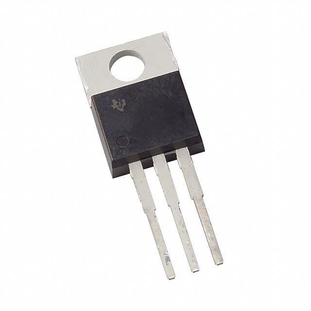
| 描述 | IC REG LDO 4.7V 0.1A SOT23-5 |
| 产品分类 | |
| 品牌 | Texas Instruments |
| 数据手册 | |
| 产品图片 |
|
| 产品型号 | TPS79147DBVREP |
| rohs | 无铅 / 符合限制有害物质指令(RoHS)规范要求 |
| 产品系列 | - |
| 供应商器件封装 | SOT-23-5 |
| 其它名称 | 296-18169-1 |
| 包装 | 剪切带 (CT) |
| 安装类型 | 表面贴装 |
| 封装/外壳 | SC-74A,SOT-753 |
| 工作温度 | -40°C ~ 125°C |
| 标准包装 | 1 |
| 电压-跌落(典型值) | 0.038V @ 100mA |
| 电压-输入 | 最高 5.5V |
| 电压-输出 | 4.7V |
| 电流-输出 | 100mA |
| 电流-限制(最小值) | 285mA |
| 稳压器拓扑 | 正,固定式 |
| 稳压器数 | 1 |


- 商务部:美国ITC正式对集成电路等产品启动337调查
- 曝三星4nm工艺存在良率问题 高通将骁龙8 Gen1或转产台积电
- 太阳诱电将投资9.5亿元在常州建新厂生产MLCC 预计2023年完工
- 英特尔发布欧洲新工厂建设计划 深化IDM 2.0 战略
- 台积电先进制程称霸业界 有大客户加持明年业绩稳了
- 达到5530亿美元!SIA预计今年全球半导体销售额将创下新高
- 英特尔拟将自动驾驶子公司Mobileye上市 估值或超500亿美元
- 三星加码芯片和SET,合并消费电子和移动部门,撤换高东真等 CEO
- 三星电子宣布重大人事变动 还合并消费电子和移动部门
- 海关总署:前11个月进口集成电路产品价值2.52万亿元 增长14.8%


PDF Datasheet 数据手册内容提取
TPS79101-EP, TPS79118-EP (cid:7)(cid:10)(cid:15)(cid:16)(cid:9)(cid:13) (cid:8)(cid:12)(cid:18)(cid:11) (cid:7)(cid:10)(cid:15)(cid:16)(cid:9)(cid:13) (cid:8)(cid:12)(cid:18)(cid:11) TPS79133-EP, TPS79147-EP (cid:2)(cid:6)(cid:4)(cid:5)(cid:5) (cid:14)(cid:14) (cid:17) (cid:6)(cid:4)(cid:5)(cid:5) (cid:14)(cid:14)(cid:3) (cid:2)(cid:6)(cid:4)(cid:5)(cid:5) (cid:14)(cid:14) (cid:17) (cid:6)(cid:4)(cid:5)(cid:5) (cid:14)(cid:14)(cid:3) www.ti.com............................................................................................................................................................ SGLS161A–APRIL2003–REVISEDJUNE2008 ULTRALOW NOISE, HIGH PSRR, FAST RF, 100-mA LOW-DROPOUT LINEAR REGULATORS FEATURES 1 • 100-mALow-DropoutRegulatorWithEN DESCRIPTION 2 • Availablein1.8-V,3.3-V,4.7-V,andAdjustable The TPS791xx family of low-dropout (LDO) Versions low-power linear voltage regulators features high • HighPSRR(70dBat10kHz) power supply rejection ratio (PSRR), ultralow noise, fast start-up, and excellent line and load transient • UltralowNoise(15m V ) RMS responses in a small outline, SOT23, package. Each • FastStart-UpTime(63m s) device in the family is stable, with a small 1-m F • StableWithAny1-m FCeramicCapacitor ceramic capacitor on the output. The family uses an advanced, proprietary BiCMOS fabrication process to • ExcellentLoad/LineTransient yield extremely low dropout voltages (e.g., 38 mV at • VeryLowDropoutVoltage 100 mA, TPS79147). Each device achieves fast (38mVatFullLoad,TPS79147) start-up times (approximately 63 m s with a 0.001-m F • 5-PinSOT23(DBV)Package bypass capacitor) while consuming very low quiescent current (170 m A typical). Moreover, when • TPS792xxProvidesENOptions the device is placed in standby mode, the supply current is reduced to less than 1 m A. The TPS79118 APPLICATIONS exhibits approximately 15 m V of output voltage RMS • VCOs noise with a 0.1-m F bypass capacitor. Applications • RF with analog components that are noise sensitive, such as portable RF electronics, benefit from the • Bluetooth™,WirelessLAN high-PSRR and low-noise features as well as the fast responsetime. SUPPORTS DEFENSE, AEROSPACE, AND MEDICAL APPLICATIONS • ControlledBaseline • OneAssembly/TestSite • OneFabricationSite • AvailableinMilitary(–55°C/125°C) TemperatureRange(1) • ExtendedProductLifeCycle • ExtendedProduct-ChangeNotification • ProductTraceability (1) Customtemperaturerangesavailable ORDERINGINFORMATION(1) T OUTPUT PACKAGE(2) ORDERABLEPARTNUMBER TOP-SIDEMARKING J VOLTAGE 1.2to5.5V TPS79101DBVREP PEUE 1.8V TPS79118DBVREP PERE –40°Cto125°C SOT23(DBV) Reelof3000 3.3V TPS79133DBVREP PESE 4.7V TPS79147DBVREP PETE –55°Cto125°C 3.3V SOT23(DBV) Reelof250 TPS79133MDBVTEP PIDM (1) Forthemostcurrentpackageandorderinginformation,seethePackageOptionAddendumattheendofthisdocument,orseetheTI websiteatwww.ti.com. (2) Packagedrawings,thermaldata,andsymbolizationareavailableatwww.ti.com/packaging. 1 Pleasebeawarethatanimportantnoticeconcerningavailability,standardwarranty,anduseincriticalapplicationsofTexas Instrumentssemiconductorproductsanddisclaimerstheretoappearsattheendofthisdatasheet. BluetoothisatrademarkofBluetoothSIG,Inc.. 2 PRODUCTIONDATAinformationiscurrentasofpublicationdate. Copyright©2003–2008,TexasInstrumentsIncorporated Products conform to specifications per the terms of the Texas Instruments standard warranty. Production processing does not On products compliant to MIL-PRF-38535, all parameters are necessarilyincludetestingofallparameters. testedunlessotherwisenoted.Onallotherproducts,production processingdoesnotnecessarilyincludetestingofallparameters.
TPS79101-EP, TPS79118-EP TPS79133-EP, TPS79147-EP SGLS161A–APRIL2003–REVISEDJUNE2008............................................................................................................................................................ www.ti.com Thesedeviceshavelimitedbuilt-inESDprotection.Theleadsshouldbeshortedtogetherorthedeviceplacedinconductivefoam duringstorageorhandlingtopreventelectrostaticdamagetotheMOSgates. DBV PACKAGE TPS79133 TPS79133 (TOP VIEW) RIPPLE REJECTION OUTPUT SPECTRAL NOISE DENSITY vs vs IN 1 5 OUT FREQUENCY FREQUENCY GND 2 100 VI = 4.3 V Hz 0.4 EN 3 4 BYPASS 90 CCo(b y=p 1) 0= m0F.01 m F V/ 0.35 VCOo == 14 .m3F V IN DFB(ixTVeO1 dPP AO VCpIKE6tiWoAnG)EOUT Ripple Rejection − dB 6574800000 IO = 10 mA IO = 100 mA mctral Noise Density − 00..00012...55123 IO = 1 mAIO = 100 mA C(byp) = 0.1 m F GND 2 5 FB pe 30 ut S 0.05 EN 3 4 BYPASS p 20 Out 0 10 100 1 k 10 k 100 k 1 M 10 M 100 1 k 10 k 100 k Adjustable Option f − Frequency − Hz f − Frequency − Hz ABSOLUTE MAXIMUM RATINGS(1) overoperatingfree-airtemperaturerange(unlessotherwisenoted) TPS79101,TPS79118, TPS79133,TPS79147 Inputvoltagerange(2) –0.3Vto6V VoltagerangeatEN –0.3VtoV +0.3V I VoltageonOUT –0.3Vto6V Peakoutputcurrent Internallylimited ESDrating,HBM 2kV ESDrating,CDM 500V Continuoustotalpowerdissipation SeeDissipationRatingTable Allothers –40°Cto150°C Operatingvirtual-junctiontemperaturerange,T J TPS79133MDBVTEP –55°Cto125°C Allothers –40°Cto120°C Operatingambienttemperaturerange,T A TPS79133MBVTEP –55°Cto125°C Storagetemperaturerange,T –65°Cto150°C stg LowK 63.75°C/W Rq JC(3) HighK 63.75°C/W LowK 256°C/W Rq JA(4) HighK 178.3°C/W (1) Stressesbeyondthoselistedunder“absolutemaximumratings”maycausepermanentdamagetothedevice.Thesearestressratings only,andfunctionaloperationofthedeviceattheseoranyotherconditionsbeyondthoseindicatedunder“recommendedoperating conditions”isnotimplied.Exposuretoabsolute-maximum-ratedconditionsforextendedperiodsmayaffectdevicereliability. (2) Allvoltagevaluesarewithrespecttonetworkgroundterminal. (3) TheJEDEClow-K(1s)boarddesignusedtoderivethisdatawasa3-inch×3-inch,two-layerboardwith2-ouncecoppertracesontop oftheboard. (4) TheJEDEChigh-K(2s2p)boarddesignusedtoderivethisdatawasa3-inch×3-inch,multilayerboardwith1-ounceinternalpowerand groundplanesand2-ouncecoppertracesontopandbottomoftheboard. 2 SubmitDocumentationFeedback Copyright©2003–2008,TexasInstrumentsIncorporated ProductFolderLink(s):TPS79101-EP TPS79118-EPTPS79133-EP TPS79147-EP
TPS79101-EP, TPS79118-EP TPS79133-EP, TPS79147-EP www.ti.com............................................................................................................................................................ SGLS161A–APRIL2003–REVISEDJUNE2008 RECOMMENDED OPERATING CONDITIONS MI MA UNI N X T Inputvoltage,V(1) 2.7 5.5 V I Continuousoutputcurrent,I (2) 0 100 mA O –40 125 Operatingjunctiontemperature,T °C J TPS79133MBVTEP –55 125 (1) Tocalculatetheminimuminputvoltageforyourmaximumoutputcurrent,usethefollowingformula:V(min)=V (max)+VDO(max I O load) (2) Continuousoutputcurrentandoperatingjunctiontemperaturearelimitedbyinternalprotectioncircuitry,butitisnotrecommendedthat thedeviceoperateunderconditionsbeyondthosespecifiedinthistableforextendedperiodsoftime. Notes: 1.Seedatasheetforabsolutemaximumandminimumrecommendedoperatingconditions. 2.Siliconoperating-lifedesigngoalis10yearsat105°Cjunctiontemperature(doesnotinclude packageinterconnectlife). 3.Enhancedplasticproductdisclaimerapplies. 1000 ElectromigrationFailMode s) 100 ar WirebondVoiding e Y FailMode ( e Lif d e at m sti 10 E 1 100 110 120 130 140 150 160 ContinuousT (°C) J Figure1.TPS79133OperatingLifeDeratingChart Copyright©2003–2008,TexasInstrumentsIncorporated SubmitDocumentationFeedback 3 ProductFolderLink(s):TPS79101-EP TPS79118-EPTPS79133-EP TPS79147-EP
TPS79101-EP, TPS79118-EP TPS79133-EP, TPS79147-EP SGLS161A–APRIL2003–REVISEDJUNE2008............................................................................................................................................................ www.ti.com ELECTRICAL CHARACTERISTICS overrecommendedoperatingfree-airtemperaturerange,(T =–40°Cto125°C),V =V (typ)+1V,I =1mA,EN=0V, J I O O C =10m F,C (byp)=0.01m F(unlessotherwisenoted) o o PARAMETER TESTCONDITIONS MIN TYP MAX UNIT T =25°C,1.22V≤V ≤5.2V V J O O TPS79101 0m A<I <100mA(1),1.22V≤V ≤5.2V 0.98V 1.02V O O O O T =25°C 1.8 J TPS79118 0m A<I <100mA,2.8V<V <5.5V 1.764 1.836 O I Outputvoltage V T =25°C 3.3 J TPS79133 0m A<I <100mA,4.3V<V <5.5V 3.234 3.366 O I T =25°C 4.7 J TPS79147 0m A<I <100mA,5.2V<V <5.5V 4.606 4.794 O I 0m A<I <100mA,T =25°C 170 Quiescentcurrent(GNDcurrent) O J m A 0m A<I <100mA 250 O Loadregulation 0m A<I <100mA,T =25°C 5 mV O J V +1V<V ≤5.5V,T =25°C 0.05 Outputvoltagelineregulation(ΔV /V )(2) O I J %/V O O V +1V<V ≤5.5V 0.12 O I C =0.001m F 32 (byp) Outputnoisevoltage(TPS79118) BW=100Hzto100kHz, C(byp)=0.0047m F 17 m V IO=100mA,TJ=25°C C(byp)=0.01m F 16 RMS C =0.1m F 15 (byp) C =0.001m F 53 (byp) Time,start-up(TPS79133) RL33Ω,CO=1m F, C =0.0047m F 67 m s T =25°C (byp) J C =0.01m F 98 (byp) Outputcurrentlimit V =0V(1) 285 600 mA O UVLOthreshold V rising 2.25 2.65 V CC UVLOhysteresis T =25°C,V rising 100 mV J CC (1) TheminimumINoperatingvoltageis2.7VorV (typ)+1V,whicheverisgreater.ThemaximumINvoltageis5.5V.Themaximum O outputcurrentis100mA. (2) IfV ≤1.8VthenV =2.7V,V =5.5V: O Imin Imax VO(cid:5)VImax(cid:2)2.7V(cid:6) Lineregulation(mV) (cid:3) (cid:5)%(cid:4)V(cid:6) (cid:1) 100 (cid:1)1000 IfV ≥2.5VthenV =V +1V,V =5.5V: O Imin O Imax VO(cid:6)VImax(cid:3)(cid:6)VO(cid:2)1V(cid:7)(cid:7) Lineregulation(mV) (cid:4) (cid:6)%(cid:5)V(cid:7) (cid:1) 100 (cid:1)1000 4 SubmitDocumentationFeedback Copyright©2003–2008,TexasInstrumentsIncorporated ProductFolderLink(s):TPS79101-EP TPS79118-EPTPS79133-EP TPS79147-EP
TPS79101-EP, TPS79118-EP TPS79133-EP, TPS79147-EP www.ti.com............................................................................................................................................................ SGLS161A–APRIL2003–REVISEDJUNE2008 ELECTRICAL CHARACTERISTICS (continued) overrecommendedoperatingfree-airtemperaturerange,(T =–40°Cto125°C),V =V (typ)+1V,I =1mA,EN=0V, J I O O C =10m F,C (byp)=0.01m F(unlessotherwisenoted) o o PARAMETER TESTCONDITIONS MIN TYP MAX UNIT Standbycurrent EN=V,2.7V<V <5.5V 0.07 1 m A I I High-levelenableinputvoltage 2.7V<V <5.5V 2 V I Low-levelenableinputvoltage 2.7V<V <5.5V 0.7 V I Inputcurrent(EN) EN=V –1 1 m A I f=100Hz,T =25°C,I =10mA 80 J O f=100Hz,T =25°C,I =100mA 75 J O TPS79118 f=10kHz,T =25°C,I =100mA 72 J O f=100kHz,T =25°C,I =100mA 45 J O Powersupplyripplerejection dB f=100Hz,T =25°C,I =10mA 70 J O f=100Hz,T =25°C,I =100mA 75 J O TPS79133 f=10kHz,T =25°C,I =100mA 73 J O f=100kHz,T =25°C,I =100mA 37 J O I =100mA,T =25°C 50 O J TPS79133 I =100mA 90 Dropoutvoltage(3) O mV I =100mA,T =25°C 38 O J TPS79147 I =100mA 70 O (3) INvoltageequalsV (typ)–100mV.TheTPS79118dropoutvoltageislimitedbytheinputvoltagerangelimitations. O Copyright©2003–2008,TexasInstrumentsIncorporated SubmitDocumentationFeedback 5 ProductFolderLink(s):TPS79101-EP TPS79118-EPTPS79133-EP TPS79147-EP
TPS79101-EP, TPS79118-EP TPS79133-EP, TPS79147-EP SGLS161A–APRIL2003–REVISEDJUNE2008............................................................................................................................................................ www.ti.com FUNCTIONALBLOCKDIAGRAM—ADJUSTABLEVERSION VIN VOUT UVLO Current Sense SHUTDOWN ILIM R1 GND _ + FB EN R2 UVLO Thermal Shutdown External to the Device Bandgap 250 kW Vref VIN Reference Bypass FUNCTIONALBLOCKDIAGRAM—FIXEDVERSION VIN VOUT UVLO Current Sense GND SHUTDOWN ILIM R1 _ + EN UVLO R2 Thermal Shutdown VIN RBeafnedregnacpe 250 kW Vref Bypass TERMINALFUNCTIONS TERMINAL I/O DESCRIPTION NAME ADJ FIXED Anexternalbypasscapacitor,connectedtothisterminal,inconjunctionwithaninternal BYPASS 4 4 resistor,createsalow-passfiltertofurtherreduceregulatornoise. TheENterminalisaninputwhichenablesorshutsdownthedevice.WhenENisalogic EN 3 3 I high,thedevicewillbeinshutdownmode.WhenENisalogiclow,thedevicewillbe enabled. FB 5 N/A I Thisterminalisthefeedbackinputvoltagefortheadjustabledevice. GND 2 2 Regulatorground IN 1 1 I TheINterminalistheinputtothedevice. OUT 6 5 O TheOUTterminalistheregulatedoutputofthedevice. 6 SubmitDocumentationFeedback Copyright©2003–2008,TexasInstrumentsIncorporated ProductFolderLink(s):TPS79101-EP TPS79118-EPTPS79133-EP TPS79147-EP
TPS79101-EP, TPS79118-EP TPS79133-EP, TPS79147-EP www.ti.com............................................................................................................................................................ SGLS161A–APRIL2003–REVISEDJUNE2008 TYPICAL CHARACTERISTICS TPS79118 TPS79133 TPS79118 OUTPUT VOLTAGE OUTPUT VOLTAGE OUTPUT VOLTAGE vs vs vs OUTPUT CURRENT OUTPUT CURRENT JUNCTION TEMPERATURE 1.803 3.303 1.82 V− Output Voltage − VO111...7881900.9128 VCTJIo === 221.508° mVCF − Output Voltage − VVO333...2333900.9123 VCTJIo === 421.503° mVCF V− Output Voltage − VO 111...11788..190178.555918 VCIo == 21.08 mVFIO = 1I0O0 = m 1A mA 1.798 3.298 1.785 1.797 3.297 1.78 0 20 40 60 80 100 0 20 40 60 80 100 −40−25−10 5 20 35 50 65 80 95 110125 IO − Output Current − mA IO − Output Current − mA TJ − Junction Temperature − °C Figure2. Figure3. Figure4. TPS79133 TPS79133 TPS79118 OUTPUT VOLTAGE GROUND CURRENT OUTPUT SPECTRAL NOISE DENSITY vs vs vs JUNCTION TEMPERATURE JUNCTION TEMPERATURE FREQUENCY 3.32 260 0.2 VI = 4.3 V VI = 4.3 V Hz V− Output Voltage − VO333...3223.8913 Co = 10 m FIO = 1I0O0 = m 1A mA mGround Current − A 111222468024000000 Co = 10 mIOF = 1 mA IO = 100 mA mV/pectral Noise Density − 0000000.......00001111.46824681 IO = 1 mIAO = 100 mA VCCIo( b= y= p2 1). 8 =m VF0.1 m F 120 ut S 0.02 3.27−40−25−10 5 20 35 50 65 80 95 110125 100−40−25−10 5 20 35 50 65 80 95110125 Outp 0 100 1 k 10 k 100 k TJ − Junction Temperature − °C TJ − Junction Temperature − °C f − Frequency − Hz Figure5. Figure6. Figure7. TPS79118 TPS79118 TPS79133 OUTPUT SPECTRAL NOISE DENSITY OUTPUT SPECTRAL NOISE DENSITY OUTPUT SPECTRAL NOISE DENSITY vs vs vs FREQUENCY FREQUENCY FREQUENCY Hz 0.25 Hz 1.2 IO = 0.001 m F VI = 2.8 V Hz 0.4 mV/Output Spectral Noise Density − 00..0001..55120 IO = 1 mIOA = 100 mAVCCIo( b= y= p2 1). 80= Vm0F.1 m F mV/Output Spectral Noise Density − 0000....012468 IOI O= =0 .I01ICOO. 0om ==0 F= 40 171.00 001m mFmmFFA mV/Output Spectral Noise Density − 0000....0000123...55551230 IO = 1 mAIO = 100 mA VCCIo( b= y= p4 1). 3 =m VF0.1 m F 100 1 k 10 k 100 k 100 1 k 10 k 100 k 100 1 k 10 k 100 k f − Frequency − Hz f − Frequency − Hz f − Frequency − Hz Figure8. Figure9. Figure10. Copyright©2003–2008,TexasInstrumentsIncorporated SubmitDocumentationFeedback 7 ProductFolderLink(s):TPS79101-EP TPS79118-EPTPS79133-EP TPS79147-EP
TPS79101-EP, TPS79118-EP TPS79133-EP, TPS79147-EP SGLS161A–APRIL2003–REVISEDJUNE2008............................................................................................................................................................ www.ti.com TYPICAL CHARACTERISTICS (continued) TPS79133 TPS79133 ROOT MEAN SQUARED OUTPUT NOISE OUTPUT SPECTRAL NOISE DENSITY OUTPUT SPECTRAL NOISE DENSITY S) vs vs vs RM BYPASS CAPACITANCE FREQUENCY FREQUENCY V( 70 BW = 100 Hz to 100 mV/HzOutput Spectral Noise Density − 0000....00000123....555512340100IO = 1 mAIO 1= k100 mA VCCIo( b1= y=0 p4 1)k. 30= Vm0F.1 m F 100 k mV/HzOutput Spectral Noise Density − 00001111........24682468012100 IO = 0.0011 m kF IOI O= =0 .I01ICVOO. I0om ===0 1F= 4 00 1471. 00.k 0301m mFVmmFFA 100 k mRMS − Root Mean Squared Output Noise − 12345600000000.001C(bypass) − BypkaHsVVzs0OO .C0 ==1a 1p3.a.83c ViVtance − m F 0.1 f − Frequency − Hz f − Frequency − Hz Figure11. Figure12. Figure13. TPS79133 TPS79133 TPS792133 OUTPUT IMPEDANCE DROPOUT VOLTAGE DROPOUT VOLTAGE vs vs vs FREQUENCY JUNCTION TEMPERATURE OUTPUT CURRENT 3 80 100 W− Output Impedance − 12..5512 VCTJIo === I 4O21.5 03=° CmV1F mA − Dropout Voltage − mV 3456700000 VCIo == 31.02 mVF, IO = 100 mA − Dropout Voltage − mV 34567890000000 VCIO = = 3 1.20 Vm F TJ = 125°CTJ = 25°C Zo 0.5 IO = 100 mA VDO 1200 IO = 10 mA VDO 20 TJ = −40°C 10 0 0 0 10 100 1 k 10 k 100 k 1 M 10 M −40−25−10 5 20 35 50 65 80 95 110125 0 0.02 0.04 0.06 0.08 0.1 f − Frequency − Hz TJ − Junction Temperature − °C IO − Output Current − A Figure14. Figure15. Figure16. TPS79101 MINIMUM REQUIRED INPUT VOLTAGE TPS79118 DROPOUT VOLTAGE vs RIPPLE REJECTION vs OUTPUT VOLTAGE vs INPUT VOLTAGE 5.2 FREQUENCY 120 VI = 3.2 V 90 IO = 100 mA e − V 4.7 Co = 10 m F 80 IO = 1 mA g − Dropout Voltage − mVDO 104680000 TTJJ =T= J −2 4=50 °1°C2C5°C nimum Required Input Volta 2334....7272 TJ = −40°TCJ = 125°CTJ = 25°C Ripple Rejection − dB 234567000000 VI = 2IO.8 =V 100 mA V 20 Mi Co = 10 m F 2.2 10 C(byp) = 0.01 m F 0 1.5 2 2.5 3 3.5 4 4.5 5 0 2.5 3 3.5 4 4.5 5 VO − Output Voltage − V 100 1 k 10 k 100 k 1 M 10 M VI − Input Voltage − V f − Frequency − Hz Figure17. Figure18. Figure19. 8 SubmitDocumentationFeedback Copyright©2003–2008,TexasInstrumentsIncorporated ProductFolderLink(s):TPS79101-EP TPS79118-EPTPS79133-EP TPS79147-EP
TPS79101-EP, TPS79118-EP TPS79133-EP, TPS79147-EP www.ti.com............................................................................................................................................................ SGLS161A–APRIL2003–REVISEDJUNE2008 TYPICAL CHARACTERISTICS (continued) TPS79118 TPS79118 TPS79133 RIPPLE REJECTION RIPPLE REJECTION RIPPLE REJECTION vs vs vs FREQUENCY FREQUENCY FREQUENCY 90 90 100 VI = 4.3 V 80 IO = 10 mA 80 IO = 10 mA 90 CCo(b y=p 1) 0= m0F.01 m F B 70 B 70 B 80 IO = 100 mA d d d n − 60 n − 60 n − 70 o o o Rejecti 4500 Rejecti 4500 Rejecti 60 Ripple 30 IO = 100 mA Ripple 30 IO = 100 mA Ripple 5400 IO = 10 mA 20 20 VI = 2.8 V VI = 2.8 V 10 CCo(b y=p 1) =m F0.01 m F 10 CCo(b y=p 1) =m F0.1 m F 30 0 0 20 100 1 k 10 k 100 k 1 M 10 M 100 1 k 10 k 100 k 1 M 10 M 10 100 1 k 10 k 100 k 1 M 10 M f − Frequency − Hz f − Frequency − Hz f − Frequency − Hz Figure20. Figure21. Figure22. TPS79133 TPS79133 TPS79133 RIPPLE REJECTION RIPPLE REJECTION OUTPUT VOLTAGE, ENABLE VOLTAGE vs vs vs FREQUENCY FREQUENCY TIME (START-UP) 100 100 3 Ripple Rejection − dB 657948000000 VCCIO( b= Iy=O p4 )1.= 3= m 1 V0F0. 0m1A m F IO = 100 mA Ripple Rejection − dB 657948000000 VCCIo( bI =Oy= p 41=). 3 =m1 FV00 .m1 Am F IO = 100 mA Voltage − VEnable Voltage − V 32021 C(byp) = 0.001 m FC(byp) =VVICTO JIO0o ==. ==0= 041 2134.05 3.7m0°3 C F V mmVFA ut 30 30 utp 1 C(byp) = 0.01 m F O 2010 100 1 k 10 k 100 k 1 M 10 M 2010 100 1 k 10 k 100 k 1 M 10 M − O 00 20 40 60 80100 120140 160180200 f − Frequency − Hz f − Frequency − Hz V t − Time − m s Figure23. Figure24. Figure25. Copyright©2003–2008,TexasInstrumentsIncorporated SubmitDocumentationFeedback 9 ProductFolderLink(s):TPS79101-EP TPS79118-EPTPS79133-EP TPS79147-EP
TPS79101-EP, TPS79118-EP TPS79133-EP, TPS79147-EP SGLS161A–APRIL2003–REVISEDJUNE2008............................................................................................................................................................ www.ti.com TYPICAL CHARACTERISTICS (continued) TPS79118 TPS79118 V m LINE TRANSIENT RESPONSE LOAD TRANSIENT RESPONSE − V e n m ut Voltag ICCOo( b =y= p 11)0 =m0 F 0m.0A1 m F Change I oltage − 20 VCIo == 21.08 mVF V − OutpO 100 D − VO Output V−200 −10 −40 V − A e m V− Input VoltagI 32..880 10 20 30 40 50 60 70 80 90 100 Current Load − 10000 2004006008001 k12 k14 k16 k18 k2 k t − Time − m s t − Time − m s Figure26. Figure27. TPS79133 TPS79133 mV LINE TRANSIENT RESPONSE LOAD TRANSIENT RESPONSE put Voltage − 200 − Change In oltage − mV 200 VCIo == 41.03 mVF − OutO−20 D VOOutput V −20 V −40 A m e − V 5.3 nt − 100 nput Voltag 4.3 ICCOo( b =y= p 11)0 =m0 F 0m.0A1 m F ddvt(cid:1)0m.4sV utput Curre 0 V− II 0 5 10 15 t2 −0 Ti2m5e −3 m0s 35 40 45 50 − OIO 0 50 100150t2 −0 0Tim25e0 −3 0m 0s350400450500 Figure28. Figure29. TPS79118 TPS79118 TPS79118 TYPICAL REGIONS OF STABILITY TYPICAL REGIONS OF STABILITY TYPICAL REGIONS OF STABILITY EQUIVALENT SERIES RESISTANCE (ESR) EQUIVALENT SERIES RESISTANCE (ESR) EQUIVALENT SERIES RESISTANCE (ESR) vs vs vs OUTPUT CURRENT OUTPUT CURRENT OUTPUT CURRENT 100 100 100 W Co = 0.47 m F W Co = 1 m F W Co = 10 m F − VI = 5.5 V − VI = 5.5 V − VI = 5.5 V ce TJ = −40 °C to 125°C ce TJ = −40 °C to 125°C ce TJ = −40 °C to 125°C an 10 an 10 an 10 sist Region of Instability sist Region of Instability sist Region of Instability e e e R R R s s s erie 1 erie 1 erie 1 S S S nt nt nt e e e al al al Equiv 0.1 Equiv 0.1 Region of Stability Equiv 0.1 Region of Stability − Region of − − R Instability R R ES 0.01 ES 0.01 ES 0.01 0 0.02 0.04 0.06 0.08 0.1 0 0.02 0.04 0.06 0.08 0.1 0 0.02 0.04 0.06 0.08 0.1 IO − Output Current − A IO − Output Current − A IO − Output Current − A Figure30. Figure31. Figure32. 10 SubmitDocumentationFeedback Copyright©2003–2008,TexasInstrumentsIncorporated ProductFolderLink(s):TPS79101-EP TPS79118-EPTPS79133-EP TPS79147-EP
TPS79101-EP, TPS79118-EP TPS79133-EP, TPS79147-EP www.ti.com............................................................................................................................................................ SGLS161A–APRIL2003–REVISEDJUNE2008 APPLICATION INFORMATION The TPS791xx family of low-dropout (LDO) regulators have been optimized for use in noise-sensitive battery-operated equipment. The device features extremely low dropout voltages, high PSRR, ultralow output noise, low quiescent current (170 m A typically), and enable-input to reduce supply currents to less than 1 m A whentheregulatoristurnedoff. AtypicalapplicationcircuitisshowninFigure33. TPS791xx 1 VI IN 4 BYPASS 5 OUT VO 0.1 m F 3 0.01 m F EN + 1 m F GND 2 Figure33.TypicalApplicationCircuit External Capacitor Requirements A 0.1-m F or larger ceramic input bypass capacitor, connected between IN and GND and located close to the TPS791xx, is required for stability and to improve transient response, noise rejection, and ripple rejection. A higher-value electrolytic input capacitor may be necessary if large, fast-rise-time load transients are anticipated andthedeviceislocatedseveralinchesfromthepowersource. Like all low dropout regulators, the TPS791xx requires an output capacitor connected between OUT and GND to stabilize the internal control loop. The minimum recommended capacitance is 1 m F. Any 1-m F or larger ceramic capacitorissuitable.Thedeviceisalsostablewitha0.47-m Fceramiccapacitorwithatleast75mΩofESR. The internal voltage reference is a key source of noise in an LDO regulator. The TPS791xx has a BYPASS pin which is connected to the voltage reference through a 250-kΩ internal resistor. The 250-kΩ internal resistor, in conjunction with an external bypass capacitor connected to the BYPASS pin, creates a low pass filter to reduce the voltage reference noise and, therefore, the noise at the regulator output. In order for the regulator to operate properly, the current flow out of the BYPASS pin must be at a minimum because any leakage current creates an IR drop across the internal resistor thus creating an output error. Therefore, the bypass capacitor must have minimalleakagecurrent. For example, the TPS79118 exhibits approximately 15 m V of output voltage noise using a 0.1-m F ceramic RMS bypass capacitor and a 1-m F ceramic output capacitor. Note that the output starts up slower as the bypass capacitance increases due to the RC time constant at the bypass pin that is created by the internal 250 kΩ resistorandexternalcapacitor. Board Layout Recommendation To Improve PSRR And Noise Performance ToimproveacmeasurementslikePSRR,outputnoise,and transient response, it is recommended that the board be designed with separate ground planes for V and V , with each ground plane connected only at the ground IN OUT pin of the device. In addition, the ground connection for the bypass capacitor should connect directly to the groundpinofthedevice. Copyright©2003–2008,TexasInstrumentsIncorporated SubmitDocumentationFeedback 11 ProductFolderLink(s):TPS79101-EP TPS79118-EPTPS79133-EP TPS79147-EP
TPS79101-EP, TPS79118-EP TPS79133-EP, TPS79147-EP SGLS161A–APRIL2003–REVISEDJUNE2008............................................................................................................................................................ www.ti.com Power Dissipation and Junction Temperature Specified regulator operation is assured to a junction temperature of 125°C; the maximum junction temperature should be restricted to 125°C under normal operating conditions. This restriction limits the power dissipation the regulator can handle in any given application. To ensure the junction temperature is within acceptable limits, calculate the maximum allowable dissipation, P , and the actual dissipation, P , which must be less than or D(max) D equaltoP . D(max) Themaximumpower-dissipationlimitisdeterminedusingthefollowingequation: T max(cid:1)T P (cid:2) J A D(max) R (cid:1)JA (1) Where: T maxisthemaximumallowablejunctiontemperature. J Rq JAisthejunction-to-ambientthermalresistanceforthepackage(seethedissipationratingtable). T istheambienttemperature. A Theregulatordissipationiscalculatedusing: PD(cid:3)(cid:4)VI(cid:2)VO(cid:5)(cid:1)IO (2) Power dissipation resulting from quiescent current is negligible. Excessive power dissipation triggers the thermal protectioncircuit. Programming the TPS79101 Adjustable LDO Regulator The output voltage of the TPS79101 adjustable regulator is programmed using an external resistor divider as showninFigure34.Theoutputvoltageiscalculatedusing: (cid:4) R1(cid:5) VO(cid:3)Vref(cid:1) 1(cid:2)R2 (3) Where: V =1.2246Vtyp(theinternalreferencevoltage) ref Resistors R1 and R2 should be chosen for approximately 50-m A divider current. Lower value resistors can be used for improved noise performance, but the solution consumes more power. Higher resistor values should be avoided as leakage current into/out of FB across R1/R2 creates an offset voltage that artificially increases/decreases the feedback voltage and thus erroneously decreases/increases V . The recommended O design procedure is to choose R2 = 30.1 kΩ to set the divider current at 50 m A, C1 = 15 pF for stability, and then calculateR1using: (cid:4)V (cid:5) O R1(cid:3) (cid:2)1 (cid:1)R2 V ref (4) In order to improve the stability of the adjustable version, it is suggested that a small compensation capacitor be placed between OUT and FB. For voltages <1.8 V, the value of this capacitor should be 100 pF. For voltages>1.8V,theapproximatevalueofthiscapacitorcanbecalculatedas: (3(cid:1)10(cid:3)7)(cid:1)(R1 (cid:2) R2) C1 (cid:4) (R1(cid:1)R2) (5) The suggested value of this capacitor for several resistor ratios is shown in the table below. If this capacitor is not used (such as in a unity-gain configuration) or if an output voltage < 1.8 V is chosen, then the minimum recommendedoutputcapacitoris2.2m Finsteadof1m F. 12 SubmitDocumentationFeedback Copyright©2003–2008,TexasInstrumentsIncorporated ProductFolderLink(s):TPS79101-EP TPS79118-EPTPS79133-EP TPS79147-EP
TPS79101-EP, TPS79118-EP TPS79133-EP, TPS79147-EP www.ti.com............................................................................................................................................................ SGLS161A–APRIL2003–REVISEDJUNE2008 TPS79101 OUTPUT VOLTAGE VI IN PROGRAMMING GUIDE 1 m F OUTPUT R1 R2 C1 VOLTAGE ≥ 2 V EN OUT C1 VO 2.5 V 31.6 kW 30.1 kW 22 pF R1 ≤ 0.7 V 1 m F 3.3 V 51 kW 30.1 kW 15 pF BYPASS FB 3.6 V 59 kW 30.1 kW 15 pF 0.01 m F GND R2 Figure34.TPS79101AdjustableLDORegulatorProgramming Regulator Protection The TPS791xx PMOS-pass transistor has a built-in back diode that conducts reverse current when the input voltage drops below the output voltage (e.g., during power down). Current is conducted from the output to the input and is not internally limited. If extended reverse voltage operation is anticipated, external limiting might be appropriate. The TPS791xx features internal current limiting and thermal protection. During normal operation, the TPS791xx limits output current to approximately 400 mA. When current limiting engages, the output voltage scales back linearly until the overcurrent condition ends. While current limiting is designed to prevent gross device failure, care should be taken not to exceed the power dissipation ratings of the package or the absolute maximum voltage ratings of the device. If the temperature of the device exceeds approximately 165°C, thermal-protection circuitry shuts it down. Once the device has cooled down to below approximately 140°C, regulator operation resumes. Copyright©2003–2008,TexasInstrumentsIncorporated SubmitDocumentationFeedback 13 ProductFolderLink(s):TPS79101-EP TPS79118-EPTPS79133-EP TPS79147-EP
PACKAGE OPTION ADDENDUM www.ti.com 6-Feb-2020 PACKAGING INFORMATION Orderable Device Status Package Type Package Pins Package Eco Plan Lead/Ball Finish MSL Peak Temp Op Temp (°C) Device Marking Samples (1) Drawing Qty (2) (6) (3) (4/5) TPS79101DBVREP ACTIVE SOT-23 DBV 6 3000 Green (RoHS NIPDAU Level-1-260C-UNLIM -40 to 125 PEUE & no Sb/Br) TPS79133DBVREP ACTIVE SOT-23 DBV 5 3000 Green (RoHS NIPDAU Level-1-260C-UNLIM -40 to 125 PESE & no Sb/Br) TPS79133MDBVTEP ACTIVE SOT-23 DBV 5 250 Green (RoHS NIPDAU Level-1-260C-UNLIM -55 to 125 PIDM & no Sb/Br) TPS79147DBVREP ACTIVE SOT-23 DBV 5 3000 Green (RoHS NIPDAU Level-1-260C-UNLIM -40 to 125 PETE & no Sb/Br) V62/03644-01YE ACTIVE SOT-23 DBV 6 3000 Green (RoHS NIPDAU Level-1-260C-UNLIM -40 to 125 PEUE & no Sb/Br) V62/03644-03XE ACTIVE SOT-23 DBV 5 3000 Green (RoHS NIPDAU Level-1-260C-UNLIM -40 to 125 PESE & no Sb/Br) V62/03644-04XE ACTIVE SOT-23 DBV 5 3000 Green (RoHS NIPDAU Level-1-260C-UNLIM -40 to 125 PETE & no Sb/Br) V62/03644-05XE ACTIVE SOT-23 DBV 5 250 Green (RoHS NIPDAU Level-1-260C-UNLIM -55 to 125 PIDM & no Sb/Br) (1) The marketing status values are defined as follows: ACTIVE: Product device recommended for new designs. LIFEBUY: TI has announced that the device will be discontinued, and a lifetime-buy period is in effect. NRND: Not recommended for new designs. Device is in production to support existing customers, but TI does not recommend using this part in a new design. PREVIEW: Device has been announced but is not in production. Samples may or may not be available. OBSOLETE: TI has discontinued the production of the device. (2) RoHS: TI defines "RoHS" to mean semiconductor products that are compliant with the current EU RoHS requirements for all 10 RoHS substances, including the requirement that RoHS substance do not exceed 0.1% by weight in homogeneous materials. Where designed to be soldered at high temperatures, "RoHS" products are suitable for use in specified lead-free processes. TI may reference these types of products as "Pb-Free". RoHS Exempt: TI defines "RoHS Exempt" to mean products that contain lead but are compliant with EU RoHS pursuant to a specific EU RoHS exemption. Green: TI defines "Green" to mean the content of Chlorine (Cl) and Bromine (Br) based flame retardants meet JS709B low halogen requirements of <=1000ppm threshold. Antimony trioxide based flame retardants must also meet the <=1000ppm threshold requirement. (3) MSL, Peak Temp. - The Moisture Sensitivity Level rating according to the JEDEC industry standard classifications, and peak solder temperature. (4) There may be additional marking, which relates to the logo, the lot trace code information, or the environmental category on the device. Addendum-Page 1
PACKAGE OPTION ADDENDUM www.ti.com 6-Feb-2020 (5) Multiple Device Markings will be inside parentheses. Only one Device Marking contained in parentheses and separated by a "~" will appear on a device. If a line is indented then it is a continuation of the previous line and the two combined represent the entire Device Marking for that device. (6) Lead/Ball Finish - Orderable Devices may have multiple material finish options. Finish options are separated by a vertical ruled line. Lead/Ball Finish values may wrap to two lines if the finish value exceeds the maximum column width. Important Information and Disclaimer:The information provided on this page represents TI's knowledge and belief as of the date that it is provided. TI bases its knowledge and belief on information provided by third parties, and makes no representation or warranty as to the accuracy of such information. Efforts are underway to better integrate information from third parties. TI has taken and continues to take reasonable steps to provide representative and accurate information but may not have conducted destructive testing or chemical analysis on incoming materials and chemicals. TI and TI suppliers consider certain information to be proprietary, and thus CAS numbers and other limited information may not be available for release. In no event shall TI's liability arising out of such information exceed the total purchase price of the TI part(s) at issue in this document sold by TI to Customer on an annual basis. Addendum-Page 2
PACKAGE MATERIALS INFORMATION www.ti.com 29-Aug-2017 TAPE AND REEL INFORMATION *Alldimensionsarenominal Device Package Package Pins SPQ Reel Reel A0 B0 K0 P1 W Pin1 Type Drawing Diameter Width (mm) (mm) (mm) (mm) (mm) Quadrant (mm) W1(mm) TPS79101DBVREP SOT-23 DBV 6 3000 180.0 9.0 3.15 3.2 1.4 4.0 8.0 Q3 TPS79133DBVREP SOT-23 DBV 5 3000 180.0 9.0 3.15 3.2 1.4 4.0 8.0 Q3 TPS79133MDBVTEP SOT-23 DBV 5 250 180.0 9.0 3.15 3.2 1.4 4.0 8.0 Q3 TPS79147DBVREP SOT-23 DBV 5 3000 180.0 9.0 3.15 3.2 1.4 4.0 8.0 Q3 PackMaterials-Page1
PACKAGE MATERIALS INFORMATION www.ti.com 29-Aug-2017 *Alldimensionsarenominal Device PackageType PackageDrawing Pins SPQ Length(mm) Width(mm) Height(mm) TPS79101DBVREP SOT-23 DBV 6 3000 182.0 182.0 20.0 TPS79133DBVREP SOT-23 DBV 5 3000 182.0 182.0 20.0 TPS79133MDBVTEP SOT-23 DBV 5 250 182.0 182.0 20.0 TPS79147DBVREP SOT-23 DBV 5 3000 182.0 182.0 20.0 PackMaterials-Page2
PACKAGE OUTLINE DBV0006A SOT-23 - 1.45 mm max height SCALE 4.000 SMALL OUTLINE TRANSISTOR C 3.0 2.6 0.1 C 1.75 1.45 B A 1.45 MAX PIN 1 INDEX AREA 1 6 2X 0.95 3.05 2.75 1.9 5 2 4 3 0.50 6X 0.25 0.15 0.2 C A B (1.1) TYP 0.00 0.25 GAGE PLANE 0.22 TYP 0.08 8 TYP 0.6 0 0.3 TYP SEATING PLANE 4214840/B 03/2018 NOTES: 1. All linear dimensions are in millimeters. Any dimensions in parenthesis are for reference only. Dimensioning and tolerancing per ASME Y14.5M. 2. This drawing is subject to change without notice. 3. Body dimensions do not include mold flash or protrusion. Mold flash and protrusion shall not exceed 0.15 per side. 4. Leads 1,2,3 may be wider than leads 4,5,6 for package orientation. 5. Refernce JEDEC MO-178. www.ti.com
EXAMPLE BOARD LAYOUT DBV0006A SOT-23 - 1.45 mm max height SMALL OUTLINE TRANSISTOR PKG 6X (1.1) 1 6X (0.6) 6 SYMM 2 5 2X (0.95) 3 4 (R0.05) TYP (2.6) LAND PATTERN EXAMPLE EXPOSED METAL SHOWN SCALE:15X SOLDER MASK SOLDER MASK METAL UNDER METAL OPENING OPENING SOLDER MASK EXPOSED METAL EXPOSED METAL 0.07 MAX 0.07 MIN ARROUND ARROUND NON SOLDER MASK SOLDER MASK DEFINED DEFINED (PREFERRED) SOLDER MASK DETAILS 4214840/B 03/2018 NOTES: (continued) 6. Publication IPC-7351 may have alternate designs. 7. Solder mask tolerances between and around signal pads can vary based on board fabrication site. www.ti.com
EXAMPLE STENCIL DESIGN DBV0006A SOT-23 - 1.45 mm max height SMALL OUTLINE TRANSISTOR PKG 6X (1.1) 1 6X (0.6) 6 SYMM 2 5 2X(0.95) 3 4 (R0.05) TYP (2.6) SOLDER PASTE EXAMPLE BASED ON 0.125 mm THICK STENCIL SCALE:15X 4214840/B 03/2018 NOTES: (continued) 8. Laser cutting apertures with trapezoidal walls and rounded corners may offer better paste release. IPC-7525 may have alternate design recommendations. 9. Board assembly site may have different recommendations for stencil design. www.ti.com
PACKAGE OUTLINE DBV0005A SOT-23 - 1.45 mm max height SCALE 4.000 SMALL OUTLINE TRANSISTOR C 3.0 2.6 0.1 C 1.75 1.45 1.45 B A 0.90 PIN 1 INDEX AREA 1 5 2X 0.95 3.05 2.75 1.9 1.9 2 4 3 0.5 5X 0.3 0.15 0.2 C A B (1.1) TYP 0.00 0.25 GAGE PLANE 0.22 TYP 0.08 8 TYP 0.6 0 0.3 TYP SEATING PLANE 4214839/E 09/2019 NOTES: 1. All linear dimensions are in millimeters. Any dimensions in parenthesis are for reference only. Dimensioning and tolerancing per ASME Y14.5M. 2. This drawing is subject to change without notice. 3. Refernce JEDEC MO-178. 4. Body dimensions do not include mold flash, protrusions, or gate burrs. Mold flash, protrusions, or gate burrs shall not exceed 0.15 mm per side. www.ti.com
EXAMPLE BOARD LAYOUT DBV0005A SOT-23 - 1.45 mm max height SMALL OUTLINE TRANSISTOR PKG 5X (1.1) 1 5 5X (0.6) SYMM (1.9) 2 2X (0.95) 3 4 (R0.05) TYP (2.6) LAND PATTERN EXAMPLE EXPOSED METAL SHOWN SCALE:15X SOLDER MASK SOLDER MASK METAL UNDER METAL OPENING OPENING SOLDER MASK EXPOSED METAL EXPOSED METAL 0.07 MAX 0.07 MIN ARROUND ARROUND NON SOLDER MASK SOLDER MASK DEFINED DEFINED (PREFERRED) SOLDER MASK DETAILS 4214839/E 09/2019 NOTES: (continued) 5. Publication IPC-7351 may have alternate designs. 6. Solder mask tolerances between and around signal pads can vary based on board fabrication site. www.ti.com
EXAMPLE STENCIL DESIGN DBV0005A SOT-23 - 1.45 mm max height SMALL OUTLINE TRANSISTOR PKG 5X (1.1) 1 5 5X (0.6) SYMM 2 (1.9) 2X(0.95) 3 4 (R0.05) TYP (2.6) SOLDER PASTE EXAMPLE BASED ON 0.125 mm THICK STENCIL SCALE:15X 4214839/E 09/2019 NOTES: (continued) 7. Laser cutting apertures with trapezoidal walls and rounded corners may offer better paste release. IPC-7525 may have alternate design recommendations. 8. Board assembly site may have different recommendations for stencil design. www.ti.com
IMPORTANTNOTICEANDDISCLAIMER TI PROVIDES TECHNICAL AND RELIABILITY DATA (INCLUDING DATASHEETS), DESIGN RESOURCES (INCLUDING REFERENCE DESIGNS), APPLICATION OR OTHER DESIGN ADVICE, WEB TOOLS, SAFETY INFORMATION, AND OTHER RESOURCES “AS IS” AND WITH ALL FAULTS, AND DISCLAIMS ALL WARRANTIES, EXPRESS AND IMPLIED, INCLUDING WITHOUT LIMITATION ANY IMPLIED WARRANTIES OF MERCHANTABILITY, FITNESS FOR A PARTICULAR PURPOSE OR NON-INFRINGEMENT OF THIRD PARTY INTELLECTUAL PROPERTY RIGHTS. These resources are intended for skilled developers designing with TI products. You are solely responsible for (1) selecting the appropriate TI products for your application, (2) designing, validating and testing your application, and (3) ensuring your application meets applicable standards, and any other safety, security, or other requirements. These resources are subject to change without notice. TI grants you permission to use these resources only for development of an application that uses the TI products described in the resource. Other reproduction and display of these resources is prohibited. No license is granted to any other TI intellectual property right or to any third party intellectual property right. TI disclaims responsibility for, and you will fully indemnify TI and its representatives against, any claims, damages, costs, losses, and liabilities arising out of your use of these resources. TI’s products are provided subject to TI’s Terms of Sale (www.ti.com/legal/termsofsale.html) or other applicable terms available either on ti.com or provided in conjunction with such TI products. TI’s provision of these resources does not expand or otherwise alter TI’s applicable warranties or warranty disclaimers for TI products. Mailing Address: Texas Instruments, Post Office Box 655303, Dallas, Texas 75265 Copyright © 2020, Texas Instruments Incorporated