ICGOO在线商城 > 集成电路(IC) > PMIC - 稳压器 - 线性 > TPS76933QDBVRQ1
 Datasheet下载
- 型号: TPS76933QDBVRQ1
- 制造商: Texas Instruments
- 库位|库存: xxxx|xxxx
- 要求:
| 数量阶梯 | 香港交货 | 国内含税 |
| +xxxx | $xxxx | ¥xxxx |
查看当月历史价格
查看今年历史价格
TPS76933QDBVRQ1产品简介:
ICGOO电子元器件商城为您提供TPS76933QDBVRQ1由Texas Instruments设计生产,在icgoo商城现货销售,并且可以通过原厂、代理商等渠道进行代购。 TPS76933QDBVRQ1价格参考。Texas InstrumentsTPS76933QDBVRQ1封装/规格:PMIC - 稳压器 - 线性, Linear Voltage Regulator IC Positive Fixed 1 Output 3.3V 100mA SOT-23-5。您可以下载TPS76933QDBVRQ1参考资料、Datasheet数据手册功能说明书,资料中有TPS76933QDBVRQ1 详细功能的应用电路图电压和使用方法及教程。
TPS76933QDBVRQ1 是 Texas Instruments(德州仪器)推出的一款线性稳压器(LDO),属于 PMIC(电源管理集成电路)系列中的低功耗、低压差线性稳压器。以下是该型号的应用场景:

 1. 汽车电子
TPS76933QDBVRQ1 符合 AEC-Q100 标准,专为汽车级应用设计。它适用于以下汽车场景:
- 信息娱乐系统:为车载音响、导航设备和多媒体显示屏提供稳定的电源。
- 高级驾驶辅助系统 (ADAS):为摄像头模块、雷达传感器和其他 ADAS 组件供电。
- 车身控制模块 (BCM):用于车窗升降器、门锁系统和灯光控制等。
- 动力总成系统:为发动机控制单元 (ECU) 和变速箱控制系统提供可靠的电源。

 2. 工业自动化
在工业领域,TPS76933QDBVRQ1 可应用于需要高稳定性和低噪声电源的场景:
- 传感器接口:为温度、压力和流量传感器提供精确的电源。
- 可编程逻辑控制器 (PLC):为 PLC 的处理器和输入/输出模块供电。
- 数据采集系统:为高精度模数转换器 (ADC) 和数模转换器 (DAC) 提供低噪声电源。

 3. 通信设备
该器件适合于通信基础设施中对电源效率和稳定性要求较高的场景:
- 基站模块:为射频 (RF) 放大器和信号处理单元供电。
- 网络交换机和路由器:为微控制器和通信接口芯片提供稳定的电源。
- 物联网 (IoT) 设备:为低功耗无线模块和传感器节点供电。

 4. 消费类电子产品
尽管 TPS76933QDBVRQ1 主要面向汽车和工业市场,但在某些高性能消费类电子产品中也有应用:
- 便携式设备:如高端耳机、智能手表等,需要低功耗和小尺寸的电源解决方案。
- 医疗设备:为便携式健康监测设备(如血压计、血糖仪)提供稳定的电源。

 5. 特点与优势
- 低静态电流:延长电池寿命,适合低功耗应用。
- 快速瞬态响应:确保负载变化时输出电压的稳定性。
- 低噪声性能:适合对电源质量要求较高的敏感电路。
- 宽输入电压范围:支持多种电源输入环境。

综上所述,TPS76933QDBVRQ1 广泛应用于汽车、工业、通信和消费类电子等领域,特别是在需要高效、稳定和低噪声电源的场景中表现出色。
| 参数 | 数值 |
| 产品目录 | 集成电路 (IC)半导体 |
| 描述 | IC REG LDO 3.3V 0.1A SOT23-5低压差稳压器 Ultralow-Power 100-mA |
| 产品分类 | |
| 品牌 | Texas Instruments |
| 产品手册 | |
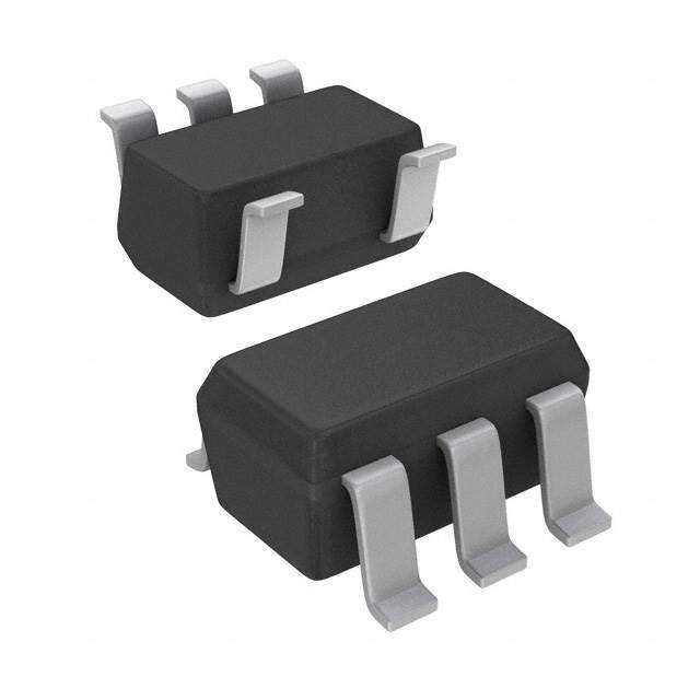
| 产品图片 |
|
| rohs | 符合RoHS无铅 / 符合限制有害物质指令(RoHS)规范要求 |
| 产品系列 | 电源管理 IC,低压差稳压器,Texas Instruments TPS76933QDBVRQ1- |
| 数据手册 | |
| 产品型号 | TPS76933QDBVRQ1 |
| 产品种类 | 低压差稳压器 |
| 供应商器件封装 | SOT-23-5 |
| 其它名称 | 296-15294-1 |
| 包装 | 剪切带 (CT) |
| 单位重量 | 13 mg |
| 商标 | Texas Instruments |
| 回动电压—最大值 | 100 mV at 50 mA |
| 安装类型 | 表面贴装 |
| 安装风格 | SMD/SMT |
| 封装 | Reel |
| 封装/外壳 | SC-74A,SOT-753 |
| 封装/箱体 | SOT-23-5 |
| 工作温度 | -40°C ~ 125°C |
| 工厂包装数量 | 3000 |
| 最大功率耗散 | 0.555 W |
| 最大工作温度 | + 125 C |
| 最大输入电压 | 10 V |
| 最小工作温度 | - 40 C |
| 最小输入电压 | + 2.7 V |
| 标准包装 | 1 |
| 电压-跌落(典型值) | 0.098V @ 100mA |
| 电压-输入 | 最高 10V |
| 电压-输出 | 3.3V |
| 电压调节准确度 | 3 % |
| 电流-输出 | 100mA |
| 电流-限制(最小值) | - |
| 稳压器拓扑 | 正,固定式 |
| 稳压器数 | 1 |
| 系列 | TPS76933-Q1 |
| 线路调整率 | 0.04 % / V |
| 负载调节 | 12 mV |
| 输入偏压电流—最大 | 0.017 mA |
| 输出电压 | 3.3 V |
| 输出电流 | 100 mA |
| 输出端数量 | 1 Output |
| 输出类型 | Fixed |
| 配用 | /product-detail/zh/TPS76933EVM-127/296-11040-ND/382259 |


- 商务部:美国ITC正式对集成电路等产品启动337调查
- 曝三星4nm工艺存在良率问题 高通将骁龙8 Gen1或转产台积电
- 太阳诱电将投资9.5亿元在常州建新厂生产MLCC 预计2023年完工
- 英特尔发布欧洲新工厂建设计划 深化IDM 2.0 战略
- 台积电先进制程称霸业界 有大客户加持明年业绩稳了
- 达到5530亿美元!SIA预计今年全球半导体销售额将创下新高
- 英特尔拟将自动驾驶子公司Mobileye上市 估值或超500亿美元
- 三星加码芯片和SET,合并消费电子和移动部门,撤换高东真等 CEO
- 三星电子宣布重大人事变动 还合并消费电子和移动部门
- 海关总署:前11个月进口集成电路产品价值2.52万亿元 增长14.8%


PDF Datasheet 数据手册内容提取
Product Sample & Technical Tools & Support & Folder Buy Documents Software Community TPS76901-Q1,TPS76912-Q1,TPS76915-Q1 TPS76918-Q1,TPS76925-Q1,TPS76927-Q1 TPS76928-Q1,TPS76930-Q1,TPS76933-Q1,TPS76950-Q1 SGLS118D–DECEMBER2001–REVISEDSEPTEMBER2016 TPS769xx-Q1 Ultralow-Power 100-mA Low-Dropout Linear Regulators 1 Features 3 Description • QualifiedforAutomotiveApplications The TPS769xx-Q1 family of low-dropout (LDO) 1 voltage regulators offers the benefits of low-dropout • 100-mALow-DropoutRegulator voltage, ultralow-power operation, and miniaturized • Availablein1.2-V,1.5-V,1.8-V,2.5-V,2.7-V, packaging. These regulators feature low-dropout 2.8‑V,3-V,3.3-Vand5-VFixed-Outputand voltages and ultralow quiescent current compared to AdjustableVersions conventional LDO regulators. Offered in a 5-pin small outline integrated-circuit SOT-23 package, the • Only17-µAQuiescentCurrentat100mA TPS769xx-Q1 series of devices are ideal for • 1-µAQuiescentCurrentinStandbyMode micropoweroperationsandwhereboardspaceisata • DropoutVoltageTypically71mVat100mA premium. • OvercurrentLimitation A combination of new circuit design and process • —40°Cto125°COperatingJunctionTemperature innovation has enabled the usual PNP pass transistor Range to be replaced by a PMOS pass element. Because the PMOS pass element behaves as a low-value • 5-PinSOT-23(DBV)Package resistor, the dropout voltage is very low, typically 71 mV at 100 mA of load current (TPS76950-Q1), 2 Applications and is directly proportional to the load current. • ADASModules Because the PMOS pass element is a voltage-driven • RFModules device, the quiescent current is ultralow (28 µA maximum) and is stable over the entire range of • WirelessModules output load current (0 mA to 100 mA). The ultralow- • GeneralNoise-SensitiveApplications dropout voltage feature and ultralow-power operation result in a significant increase in system battery operating life, making this device suitable for use in automotiveapplications. DeviceInformation(1) PARTNUMBER PACKAGE BODYSIZE(NOM) TPS769xx-Q1 SOT-23(5) 2.90mm×1.60mm (1) For all available packages, see the orderable addendum at theendofthedatasheet. FunctionalBlockDiagrams TPS76933-Q1GroundCurrentvsFree-Air Temperature TPS76901-Q1 22 IN OUT VI= 4.3 V EN 21 CO= 4.7µF Current Limit / Thermal VREF Protection 20 GND FB A µ IO= 100 mA − 19 nt e urr C 18 TPS769xx-Q1 d un IO= 0 mA o IN OUT Gr 17 EN CurrentLimit 16 / Thermal VREF Protection GND 15 −60 −40 −20 0 20 40 60 80 100 120 140 TA−Free-AirTemperature−°C Copyright © 2016,Texas Instruments Incorporated 1 An IMPORTANT NOTICE at the end of this data sheet addresses availability, warranty, changes, use in safety-critical applications, intellectualpropertymattersandotherimportantdisclaimers.PRODUCTIONDATA.
TPS76901-Q1,TPS76912-Q1,TPS76915-Q1 TPS76918-Q1,TPS76925-Q1,TPS76927-Q1 TPS76928-Q1,TPS76930-Q1,TPS76933-Q1,TPS76950-Q1 SGLS118D–DECEMBER2001–REVISEDSEPTEMBER2016 www.ti.com Table of Contents 1 Features.................................................................. 1 8.4 DeviceFunctionalModes........................................10 2 Applications........................................................... 1 9 ApplicationandImplementation........................ 11 3 Description............................................................. 1 9.1 ApplicationInformation............................................11 4 RevisionHistory..................................................... 2 9.2 TypicalApplication..................................................11 5 Description(continued)......................................... 3 10 PowerSupplyRecommendations..................... 13 6 PinConfigurationandFunctions......................... 3 11 Layout................................................................... 14 11.1 LayoutGuidelines.................................................14 7 Specifications......................................................... 3 11.2 LayoutExample....................................................14 7.1 AbsoluteMaximumRatings......................................3 11.3 PowerDissipationandJunctionTemperature......14 7.2 ESDRatings..............................................................3 12 DeviceandDocumentationSupport................. 15 7.3 RecommendedOperatingConditions.......................4 7.4 ThermalInformation..................................................4 12.1 RelatedLinks........................................................15 7.5 ElectricalCharacteristics...........................................4 12.2 ReceivingNotificationofDocumentationUpdates15 7.6 DissipationRatings...................................................6 12.3 CommunityResources..........................................15 7.7 TypicalCharacteristics..............................................6 12.4 Trademarks...........................................................15 12.5 ElectrostaticDischargeCaution............................15 8 DetailedDescription............................................ 10 12.6 Glossary................................................................15 8.1 Overview.................................................................10 13 Mechanical,Packaging,andOrderable 8.2 FunctionalBlockDiagrams.....................................10 Information........................................................... 15 8.3 FeatureDescription.................................................10 4 Revision History NOTE:Pagenumbersforpreviousrevisionsmaydifferfrompagenumbersinthecurrentversion. ChangesfromRevisionC(June2012)toRevisionD Page • AddedESDRatingstable,ThermalInformationtable,FeatureDescriptionsection,DeviceFunctionalModes, ApplicationandImplementationsection,PowerSupplyRecommendationssection,Layoutsection,Deviceand DocumentationSupportsection,andMechanical,Packaging,andOrderableInformationsection....................................... 1 • RemovedOrderingInformationtable,seePOAattheendofthedatasheet........................................................................ 1 ChangesfromRevisionB(April2008)toRevisionC Page • ChangedTPS769xxpartnamestoTPS769xx-Q1intextandimages.................................................................................. 3 • UpdatedFigures17and19toincluderegionofInstabilitybelow0.2Ω................................................................................ 9 2 SubmitDocumentationFeedback Copyright©2001–2016,TexasInstrumentsIncorporated ProductFolderLinks:TPS76901-Q1TPS76912-Q1 TPS76915-Q1 TPS76918-Q1 TPS76925-Q1 TPS76927-Q1 TPS76928-Q1 TPS76930-Q1 TPS76933-Q1 TPS76950-Q1
TPS76901-Q1,TPS76912-Q1,TPS76915-Q1 TPS76918-Q1,TPS76925-Q1,TPS76927-Q1 TPS76928-Q1,TPS76930-Q1,TPS76933-Q1,TPS76950-Q1 www.ti.com SGLS118D–DECEMBER2001–REVISEDSEPTEMBER2016 5 Description (continued) The TPS769xx-Q1 devices also feature a logic-enabled sleep mode to shut down the regulator, reducing quiescent current to 1 µA (typical) at T = 25°C. The TPS769xx-Q1 devices are offered in 1.2-V, 1.5-V, 1.8-V, J 2.5‑V, 2.7-V, 2.8-V, 3-V, 3.3-V, and 5-V fixed-voltage versions and in a variable version (programmable over the rangeof1.2Vto5.5V). 6 Pin Configuration and Functions DBVPackage 5-PinSOT-23 TopView IN 1 5 OUT GND 2 EN 3 4 FB/NC Not to scale PinFunctions PIN I/O DESCRIPTION NO. NAME 1 IN I Inputsupplyvoltage 2 GND — Ground 3 EN I Enableinput Feedbackvoltage(TPS76901-Q1only) 4 FB/NC I Noconnection(Fixedoptionsonly) 5 OUT O Regulatedoutputvoltage 7 Specifications 7.1 Absolute Maximum Ratings overoperatingfree-airtemperaturerange(unlessotherwisenoted)(1) MIN MAX UNIT Inputvoltage(2) –0.3 13.5 V VoltagerangeatEN –0.3 V +0.3 V I VoltageonOUT,FB 7 V Peakoutputcurrent InternallyLimited Continuoustotalpowerdissipation SeeDissipationRatings T Operatingvirtualjunctiontemperature –40 150 °C J T Storagetemperature –65 150 °C stg (1) StressesbeyondthoselistedunderAbsoluteMaximumRatingsmaycausepermanentdamagetothedevice.Thesearestressratings only,andfunctionaloperationofthedeviceattheseoranyotherconditionsbeyondthoseindicatedunderRecommendedOperating Conditionsisnotimplied.Exposuretoabsolute-maximum-ratedconditionsforextendedperiodsmayaffectdevicereliability. (2) Allvoltagevaluesarewithrespecttonetworkgroundterminal. 7.2 ESD Ratings VALUE UNIT Human-bodymodel(HBM),perANSI/ESDA/JEDECJS-001(1) ±2000 V Electrostaticdischarge V (ESD) Charged-devicemodel(CDM),perJEDECspecificationJESD22-C101(2) ±YYY (1) JEDECdocumentJEP155statesthat500-VHBMallowssafemanufacturingwithastandardESDcontrolprocess. (2) JEDECdocumentJEP157statesthat250-VCDMallowssafemanufacturingwithastandardESDcontrolprocess. Copyright©2001–2016,TexasInstrumentsIncorporated SubmitDocumentationFeedback 3 ProductFolderLinks:TPS76901-Q1TPS76912-Q1 TPS76915-Q1 TPS76918-Q1 TPS76925-Q1 TPS76927-Q1 TPS76928-Q1 TPS76930-Q1 TPS76933-Q1 TPS76950-Q1
TPS76901-Q1,TPS76912-Q1,TPS76915-Q1 TPS76918-Q1,TPS76925-Q1,TPS76927-Q1 TPS76928-Q1,TPS76930-Q1,TPS76933-Q1,TPS76950-Q1 SGLS118D–DECEMBER2001–REVISEDSEPTEMBER2016 www.ti.com 7.3 Recommended Operating Conditions overoperatingfree-airtemperaturerange(unlessotherwisenoted) MIN MAX UNIT V Inputvoltage(1) 2.7 10 V I V Outputvoltage 1.2 5.5 V O I Continuousoutputcurrent(2) 0 100 mA O T Operatingjunctiontemperature —40 125 °C J (1) Tocalculatetheminimuminputvoltageforyourmaximumoutputcurrent,usethefollowingformula:V(min)=V (max)+V (maxload) I O DO (2) Continuousoutputcurrentandoperatingjunctiontemperaturearelimitedbyinternalprotectioncircuitry,butitisnotrecommendedthat thedeviceoperateunderconditionsbeyondthosespecifiedinthistableforextendedperiodsoftime. 7.4 Thermal Information TPS769xx-Q1 THERMALMETRIC(1) DBV(SOT-23) UNIT 5PINS R Junction-to-ambientthermalresistance 204.6 °C/W θJA R Junction-to-case(top)thermalresistance 117.5 °C/W θJC(top) R Junction-to-boardthermalresistance 34.4 °C/W θJB ψ Junction-to-topcharacterizationparameter 11.8 °C/W JT ψ Junction-to-boardcharacterizationparameter 33.5 °C/W JB R Junction-to-case(bottom)thermalresistance — °C/W θJC(bot) (1) Formoreinformationabouttraditionalandnewthermalmetrics,seetheSemiconductorandICPackageThermalMetricsapplication report. 7.5 Electrical Characteristics overrecommendedoperatingfree-airtemperaturerange,V =V (typ)+1V,I =100mA,EN=0V,C =4.7µF(unless I O O o otherwisenoted) PARAMETER TESTCONDITIONS MIN TYP MAX UNIT 1.2V≤V ≤5.5V,T =25°C V O J O TPS76901-Q1 1.2V≤V ≤5.5V,T =–40°Cto125°C 0.97V 1.03V O J O O T =25°C,2.7V<V <10V 1.224 J IN TPS76912-Q1 T =–40°Cto125°C,2.7V<V <10V 1.187 1.261 J IN T =25°C,2.7V<V <10V 1.5 J IN TPS76915-Q1 T =–40°Cto125°C,2.7V<V <10V 1.455 1.545 J IN T =25°C,2.8V<V <10V 1.8 J IN TPS76918-Q1 T =–40°Cto125°C,2.8V<V <10V 1.746 1.854 J IN T =25°C,3.5V<V <10V 2.5 J IN TPS76925-Q1 Outputvoltage T =–40°Cto125°C,3.5V<V <10V 2.425 2.575 J IN (10∝Ato100mA V load)(1) TJ=25°C,3.7V<VIN<10V 2.7 TPS76927-Q1 T =–40°Cto125°C,3.7V<V <10V 2.619 2.781 J IN T =25°C,3.8V<V <10V 2.8 J IN TPS76928-Q1 T =–40°Cto125°C,3.8V<V <10V 2.716 2.884 J IN T =25°C,4V<V <10V 3 J IN TPS76930-Q1 T =–40°Cto125°C,4V<V <10V 2.91 3.09 J IN T =25°C,4.3V<V <10V 3.3 J IN TPS76933-Q1 T =–40°Cto125°C,4.3V<V <10V 3.201 3.399 J IN T =25°C,6V<V <10V 5 J IN TPS76950-Q1 T =—40°Cto125°C,6V<V <10V 4.85 5.15 J IN (1) MinimumINoperatingvoltageis2.7VorV (typ)+1V,whicheverisgreater.ThemaximumINvoltageis10V,minimumoutputcurrent O is10µA,andmaximumoutputcurrentis100mA. 4 SubmitDocumentationFeedback Copyright©2001–2016,TexasInstrumentsIncorporated ProductFolderLinks:TPS76901-Q1TPS76912-Q1 TPS76915-Q1 TPS76918-Q1 TPS76925-Q1 TPS76927-Q1 TPS76928-Q1 TPS76930-Q1 TPS76933-Q1 TPS76950-Q1
TPS76901-Q1,TPS76912-Q1,TPS76915-Q1 TPS76918-Q1,TPS76925-Q1,TPS76927-Q1 TPS76928-Q1,TPS76930-Q1,TPS76933-Q1,TPS76950-Q1 www.ti.com SGLS118D–DECEMBER2001–REVISEDSEPTEMBER2016 Electrical Characteristics (continued) overrecommendedoperatingfree-airtemperaturerange,V =V (typ)+1V,I =100mA,EN=0V,C =4.7µF(unless I O O o otherwisenoted) PARAMETER TESTCONDITIONS MIN TYP MAX UNIT Quiescentcurrent EN=0V,0mA<IO<100mA,TJ=25°C 17 (GNDcurrent)(1)(2) EN=0V,I =100mA,T =–40°Cto125°C 28 µA O J Loadregulation EN=0V,I =0to100mA,T =25°C 12 mV O J Outputvoltagelineregulation VO+1V<VI≤10V,TJ=25°C(1) 0.04 (∆VO/VO)(2) VO+1V<VI≤10V,TJ=–40°Cto125°C(1) 0.1 %/V Outputnoisevoltage BW=300Hzto50kHz,C =10∝F,T =25°C 190 µV o J rms Outputcurrentlimit V =0V(1) 350 750 mA O EN=V,2.7<V <10V 1 I I Standbycurrent µA T =—40°Cto125°C 2 J FBinputcurrent FB=1.224V(TPS76901-Q1) –1 1 µA Highlevelenableinputvoltage 2.7V<V <10V 1.7 V I Lowlevelenableinputvoltage 2.7V<V <10V 0.9 V I Powersupplyripplerejection f=1kHz,C =10∝F,T =25°C 60 dB o J EN=0V –1 0 1 Inputcurrent(EN) µA EN=V –1 1 I I =50mA,T =25°C 60 O J I =50mA,T =–40°Cto125°C 125 O J TPS76928-Q1 I =100mA,T =25°C 122 O J I =100mA,T =–40°Cto125°C 245 O J I =50mA,T =25°C 57 O J I =50mA,T =–40°Cto125°C 115 O J TPS76930-Q1 I =100mA,T =25°C 115 O J I =100mA,T =–40°Cto125°C 230 Dropoutvoltage(3) O J mV I =50mA,T =25°C 48 O J I =50mA,T =–40°Cto125°C 100 O J TPS76933-Q1 I =100mA,T =25°C 98 O J I =100mA,T =–40°Cto125°C 200 O J I =50mA,T =25°C 35 O J I =50mA,T =–40°Cto125°C 85 O J TPS76950-Q1 I =100mA,T =25°C 71 O J I =100mA,T =–40°Cto125°C 170 O J (2) IfV ≤1.8VthenV =2.7V,V =10V: O Imin VImax(V -2.7V) LineReg.(mV)=(%/V)´ O lmax ´1000 100 IfV ≥2.5VthenV =V +1V,V =10V: O Imin O V (IVmax -(V +1V)) LineReg.(mV)=(%/V)´ O lmax O ´1000 100 (3) TheINvoltageequalsV (typ)—100mV;theTPS76901-Q1outputvoltageissetto3.3Vnominalwithanexternalresistordivider. O TPS76912-Q1,TPS76915-Q1,TPS76918-Q1,TPS76925-Q1,andTPS76927-Q1dropoutvoltageislimitedbyinputvoltagerange limitations. Copyright©2001–2016,TexasInstrumentsIncorporated SubmitDocumentationFeedback 5 ProductFolderLinks:TPS76901-Q1TPS76912-Q1 TPS76915-Q1 TPS76918-Q1 TPS76925-Q1 TPS76927-Q1 TPS76928-Q1 TPS76930-Q1 TPS76933-Q1 TPS76950-Q1
TPS76901-Q1,TPS76912-Q1,TPS76915-Q1 TPS76918-Q1,TPS76925-Q1,TPS76927-Q1 TPS76928-Q1,TPS76930-Q1,TPS76933-Q1,TPS76950-Q1 SGLS118D–DECEMBER2001–REVISEDSEPTEMBER2016 www.ti.com 7.6 Dissipation Ratings T ≤25°C T =70°C T =85°C DERATINGFACTOR A A A BOARD PACKAGE R R POWER POWER POWER θJC θJA ABOVET =25°C A RATING RATING RATING LowK(1) DBV 65.8°C/W 259°C/W 3.9mW/°C 386mW 212mW 154mW HighK(2) DBV 65.8°C/W 180°C/W 5.6mW/°C 555mW 305mW 222mW (1) TheJEDECLowK(1s)boarddesignusedtoderivethisdatawasa3inchx3inch,twolayerboardwith2ouncecoppertracesontop oftheboard. (2) TheJEDECHighK(2s2p)boarddesignusedtoderivethisdatawasa3inchx3inch,multilayerboardwith1ounceinternalpowerand groundplanesand2ouncecoppertracesontopandbottomoftheboard. 7.7 Typical Characteristics 2.498 1.498 VI= 3.5 V VI= 2.7 V 2.496 CTAO== 2 45.7°CµF 1.496 TCAO== 2 45.7° CµF 2.494 1.494 V V − 2.492 − ge ge 1.492 Volta 2.490 Volta ut ut 1.490 p p ut 2.488 ut O O − − O O 1.488 V 2.486 V 2.484 1.486 2.482 1.484 0 20 40 60 80 100 0 20 40 60 80 100 IO−Output Current−mA IO−Output Current−mA Figure1.TPS76925-Q1OutputVoltagevsOutputCurrent Figure2.TPS76915-Q1OutputVoltagevsOutputCurrent 3.284 1.496 VI= 4.3 V 3.282 CTAO== 245.7° CµF 1.494 IO= 1 mA VI= 2.7 V 1.492 CO= 4.7 µF 3.280 V V − − 1.490 Output Voltage 33..227786 Output Voltage 11..448868 V−O 3.274 V−O1.484 IO= 100 mA 3.272 1.482 3.270 1.480 0 20 40 60 80 100 −60 −40 −20 0 20 40 60 80 100 120 140 IO−Output Current−mA TA−Free-AirTemperature−°C Figure3.TPS76933-Q1OutputVoltagevsOutputCurrent Figure4.TPS76915-Q1OutputVoltagevsFree-Air Temperature 6 SubmitDocumentationFeedback Copyright©2001–2016,TexasInstrumentsIncorporated ProductFolderLinks:TPS76901-Q1TPS76912-Q1 TPS76915-Q1 TPS76918-Q1 TPS76925-Q1 TPS76927-Q1 TPS76928-Q1 TPS76930-Q1 TPS76933-Q1 TPS76950-Q1
TPS76901-Q1,TPS76912-Q1,TPS76915-Q1 TPS76918-Q1,TPS76925-Q1,TPS76927-Q1 TPS76928-Q1,TPS76930-Q1,TPS76933-Q1,TPS76950-Q1 www.ti.com SGLS118D–DECEMBER2001–REVISEDSEPTEMBER2016 Typical Characteristics (continued) 2.496 3.285 2.494 IO= 1 mA 3.280 IO= 1 mA 2.492 2.490 VI= 4.3 V −V −V 3.275 CO= 4.7 µF −Output Voltage 222...444888846 IO= 100 mA −Output Voltage 33..226750 IO= 100 mA O2.482 O V V 2.480 VI= 3.5 V 3.260 2.478 CO= 4.7 µF 2.476 3.255 −60 −40 −20 0 20 40 60 80 100 120 140 −60 −40 −20 0 20 40 60 80 100 120 140 TA−Free-AirTemperature−°C TA−Free-AirTemperature−°C Figure5.TPS76925-Q1OutputVoltagevsFree-Air Figure6.TPS76933-Q1OutputVoltagevsFree-Air Temperature Temperature 22 2 VI= 4.3 V 1.8 21 CO= 4.7 µF Hz 1.6 ICOO== 1 1 m0 AµF 20 µV 1.4 CIOO== 1 40.07 mµFA Ground Current−µA 111987 IO= 100 mA IO= 0 mA pectral Noise Density− 010...6281 ICOO== 1 4 m.7A µF S ut 0.4 p 16 ut O 0.2 VI= 4.3 V ICOO== 1 1000 µmFA 15 0 −60 −40 −20 0 20 40 60 80 100 120 140 100 1k 10k 100k TA−Free-AirTemperature−°C f−Frequency−Hz Figure7.TPS76933-Q1GroundCurrentvsFree-Air Figure8.TPS76933-Q1OutputSpectralNoiseDensityvs Temperature Frequency 2 1000 VI= 4.3 V VI= 3.2 V 1.8 CO= 4.7 µF CO= 4.7 µF ESR = 0.3Ω 1.6 TA= 25°C Ω 1.4 mV 100 pedance− 1.21 Voltage− IO= 100 mA −OuZtput Imo 00..68 IO= 1 mA V−DropoutDO 10 IO= 10 mA 0.4 IO= 100 mA 0.2 0 1 10 100 1 k 10 k 100k 1M −60 −40 −20 0 20 40 60 80 100 120 140 f−Frequency−Hz TA−Free-AirTemperature−°C Figure9.OutputImpedancevsFrequency Figure10.TPS76933-Q1DropoutVoltagevsFree-Air Temperature Copyright©2001–2016,TexasInstrumentsIncorporated SubmitDocumentationFeedback 7 ProductFolderLinks:TPS76901-Q1TPS76912-Q1 TPS76915-Q1 TPS76918-Q1 TPS76925-Q1 TPS76927-Q1 TPS76928-Q1 TPS76930-Q1 TPS76933-Q1 TPS76950-Q1
TPS76901-Q1,TPS76912-Q1,TPS76915-Q1 TPS76918-Q1,TPS76925-Q1,TPS76927-Q1 TPS76928-Q1,TPS76930-Q1,TPS76933-Q1,TPS76950-Q1 SGLS118D–DECEMBER2001–REVISEDSEPTEMBER2016 www.ti.com Typical Characteristics (continued) 100 90 80 EN 70 dB 60 IO= 1 mA − n o 50 Rejecti 40 ple 30 p Ri 20 IO= 100 mA 10 VI= 4.3 V VO CO= 4.7 µF 0 ESR = 0.3Ω −10 10 100 1 k 10 k 100 k 1 M 10 M 0 20 40 60 80 100 120 140 160 180 200 f−Frequency−Hz t−Time−µs Figure11.TPS76933-Q1RippleRejectionvsFrequency Figure12.LDOStart-UpTime V m − A −OutputVoltage −11000 Current Load−m 1000 O V 3.7 V m − V ge 0 ut Voltage− 2.7 IL= 10 mA Change In OutputVolta−200 VI= 2.7 V −Inp ECSOR= = 4 0.7.3 µΩF −VO −400 CESOR= = 1 00. 3µFΩ VI ∆ 0 20 40 60 80 100 120 140 160 180 200 0 20 40 60 80 100 120 140 160 180 200 t−Time−µs t−Time−µs Figure13.TPS76915-Q1LineTransientResponse Figure14.TPS76915-Q1LoadTransientResponse V m − A −OutputVoltage −11000 Current Load−m 1000 O V VI= 4.3 V 5.3 CO= 4.7 µF mV ESR = 0.3Ω − V−Input Voltage−VI 4.3 EICLSO=R = 1= 04 0 .m7.3 AµΩF ∆−Change InVOOutputVoltage−1100000 0 20 40 60 80 100 120 140 160 180 0 20 40 60 80 100 120 140 160 180 t−Time−µs t−Time−µs Figure15.TPS76933-Q1LineTransientResponse Figure16.TPS76933-Q1LoadTransientResponse 8 SubmitDocumentationFeedback Copyright©2001–2016,TexasInstrumentsIncorporated ProductFolderLinks:TPS76901-Q1TPS76912-Q1 TPS76915-Q1 TPS76918-Q1 TPS76925-Q1 TPS76927-Q1 TPS76928-Q1 TPS76930-Q1 TPS76933-Q1 TPS76950-Q1
TPS76901-Q1,TPS76912-Q1,TPS76915-Q1 TPS76918-Q1,TPS76925-Q1,TPS76927-Q1 TPS76928-Q1,TPS76930-Q1,TPS76933-Q1,TPS76950-Q1 www.ti.com SGLS118D–DECEMBER2001–REVISEDSEPTEMBER2016 Typical Characteristics (continued) 100 100 VIN= 4.3 V VIN= 4.3 V CO= 4.7 µF CO= 4.7 µF 3.3 V LDO IL= 100 mA Ω Ω − − Series Resistance 10 Region of Instability Series Resistance 10 RegionofInstability Equivalent 1 RegionofStability Equivalent − − Region of Stability R R S S E E 0.2 0.1 1 0 25 50 75 100 0 0.1 0.2 0.3 0.4 0.5 0.6 0.7 0.8 0.9 1 IO−Output Current−mA Added Ceramic Capacitance−µF Figure17.TPS76933-Q1TypicalRegionsofStability Figure18.TPS76933-Q1TypicalRegionsofStability EquivalentSeriesResistance(ESR)vsOutputCurrent EquivalentSeriesResistance(ESR)vsAddedCeramic Capacitance 100 100 VIN= 4.3 V VIN= 4.3 V CO= 10 µF CO= 10 µF 3.3 V LDO IL= 100 mA Ω Ω − − Series Resistance 10 RegionofInstability Series Resistance 10 Region of Instability Equivalent 1 Region of Stability Equivalent − − Region of Stability R R S S E E 0.2 0.1 1 0 25 50 75 100 0 0.1 0.2 0.3 0.4 0.5 0.6 0.7 0.8 0.9 1 IO−Output Current−mA Added Ceramic Capacitance−µF Figure19.TPS76933-Q1TypicalRegionsofStability Figure20.TPS76933-Q1TypicalRegionsofStability EquivalentSeriesResistance(ESR)vsOutputCurrent EquivalentSeriesResistance(ESR)vsAddedCeramic Capacitance Copyright©2001–2016,TexasInstrumentsIncorporated SubmitDocumentationFeedback 9 ProductFolderLinks:TPS76901-Q1TPS76912-Q1 TPS76915-Q1 TPS76918-Q1 TPS76925-Q1 TPS76927-Q1 TPS76928-Q1 TPS76930-Q1 TPS76933-Q1 TPS76950-Q1
TPS76901-Q1,TPS76912-Q1,TPS76915-Q1 TPS76918-Q1,TPS76925-Q1,TPS76927-Q1 TPS76928-Q1,TPS76930-Q1,TPS76933-Q1,TPS76950-Q1 SGLS118D–DECEMBER2001–REVISEDSEPTEMBER2016 www.ti.com 8 Detailed Description 8.1 Overview The TPS769xx-Q1 family of low-dropout (LDO) regulators are optimized for use in battery-operated equipment and automotive applications. They feature extremely low dropout voltages, low quiescent current (17 µA nominally),andenableinputstoreducesupplycurrentsto1µAwhentheregulatorsareturnedoff. 8.2 Functional Block Diagrams IN OUT EN Current Limit / Thermal VREF Protection FB GND Copyright © 2016,Texas Instruments Incorporated Figure21. TPS76901-Q1FunctionalBlockDiagram IINN OOUUTT EENN CCuurrrreennttLLiimmiitt // TThheerrmmaall VVRREEFF PPrrootteeccttiioonn GGNNDD CCooppyyrriigghhtt ©© 22001166,,TTeexxaass IInnssttrruummeennttss IInnccoorrppoorraatteedd Figure22. TPS769xx-Q1FunctionalBlockDiagram 8.3 Feature Description 8.3.1 RegulatorProtection The TPS769xx-Q1 PMOS-pass transistor has a built-in back diode that conducts reverse current when the input voltage drops below the output voltage (for example, during power down). Current is conducted from the output to the input and is not internally limited. If extended reverse voltage operation is anticipated, external limiting mightbeappropriate. The TPS769xx-Q1 features internal current limiting and thermal protection. During normal operation, the TPS769xx-Q1 limits output current to approximately 350 mA. When current limiting engages, the output voltage scales back linearly until the overcurrent condition ends. While current limiting is designed to prevent gross device failure, care must be taken not to exceed the power dissipation ratings of the package. If the temperature of the device exceeds approximately 165°C, thermal-protection circuitry shuts it down. Once the device has cooleddowntobelowapproximately140°C,regulatoroperationresumes. 8.4 Device Functional Modes At 100-mA loads the device operates in low power mode and the quiescent current consumption is reduced to 28µA(maximum). 10 SubmitDocumentationFeedback Copyright©2001–2016,TexasInstrumentsIncorporated ProductFolderLinks:TPS76901-Q1TPS76912-Q1 TPS76915-Q1 TPS76918-Q1 TPS76925-Q1 TPS76927-Q1 TPS76928-Q1 TPS76930-Q1 TPS76933-Q1 TPS76950-Q1
TPS76901-Q1,TPS76912-Q1,TPS76915-Q1 TPS76918-Q1,TPS76925-Q1,TPS76927-Q1 TPS76928-Q1,TPS76930-Q1,TPS76933-Q1,TPS76950-Q1 www.ti.com SGLS118D–DECEMBER2001–REVISEDSEPTEMBER2016 9 Application and Implementation NOTE Information in the following applications sections is not part of the TI component specification, and TI does not warrant its accuracy or completeness. TI’s customers are responsible for determining suitability of components for their purposes. Customers should validateandtesttheirdesignimplementationtoconfirmsystemfunctionality. 9.1 Application Information The TPS769xx-Q1 uses a PMOS pass element to dramatically reduce both dropout voltage and supply current overmoreconventionalPNP-pass-elementLDOdesigns.ThePMOSpasselementisavoltage-controlleddevice and, unlike a PNP transistor, it does not require increased drive current as output current increases. Supply currentintheTPS769xx-Q1isessentiallyconstantfromnoloadtomaximumload. Current limiting and thermal protection prevent damage by excessive output current and/or power dissipation. The device switches into a constant-current mode at approximately 350 mA; further load reduces the output voltage instead of increasing the output current. The thermal protection shuts the regulator off if the junction temperature rises above approximately 165°C. Recovery is automatic when the junction temperature drops approximately 25°C below the high temperature trip point. The PMOS pass element includes a back gate diode thatconductsreversecurrentwhentheinputvoltageleveldropsbelowtheoutputvoltagelevel. A voltage of 1.7 V or greater on the EN input disables the TPS769xx-Q1 internal circuitry, reducing the supply current to 1 µA. A voltage of less than 0.9 V on the EN input enables the TPS769xx and enables normal operation to resume. The EN input does not include any deliberate hysteresis, and it exhibits an actual switching thresholdofapproximately1.5V. 9.2 Typical Application TPS769xx-Q1 1 VI IN 4 NC/FB 5 C1 OUT VO 1 µF 3 EN + 4.7 µF GND 2 ESR = 0.2Ω Copyright © 2016,Texas Instruments Incorporated TPS76912-Q1,TPS76915-Q1,TPS76918-Q1,TPS76925-Q1,TPS76927-Q1,TPS76928-Q1,TPS76930-Q1, TPS76933-Q1,TPS76950-Q1(fixed-voltageoptions). Figure23. TypicalApplicationCircuit Copyright©2001–2016,TexasInstrumentsIncorporated SubmitDocumentationFeedback 11 ProductFolderLinks:TPS76901-Q1TPS76912-Q1 TPS76915-Q1 TPS76918-Q1 TPS76925-Q1 TPS76927-Q1 TPS76928-Q1 TPS76930-Q1 TPS76933-Q1 TPS76950-Q1
TPS76901-Q1,TPS76912-Q1,TPS76915-Q1 TPS76918-Q1,TPS76925-Q1,TPS76927-Q1 TPS76928-Q1,TPS76930-Q1,TPS76933-Q1,TPS76950-Q1 SGLS118D–DECEMBER2001–REVISEDSEPTEMBER2016 www.ti.com Typical Application (continued) 9.2.1 DesignRequirements Table1liststhedesignparametersforthisexample. Table1.DesignParameters PARAMETER EXAMPLEVALUE Inputvoltagerange 4Vto10V Outputvoltage 2.5Vto5V Outputcurrentrating 100mA Outputcapacitor 4.7µFto10µF OutputcapacitorESDrange 200mΩto10Ω 9.2.2 DetailedDesignProcedure 9.2.2.1 ExternalCapacitorRequirements Although not required, TI recommends a 0.047-µF or larger ceramic input bypass capacitor, connected between IN and GND and located close to the TPS769xx-Q1, to improve transient response and noise rejection. A higher- value electrolytic input capacitor may be necessary if large, fast-rise-time load transients are anticipated and the deviceislocatedseveralinchesfromthepowersource. Like all low dropout regulators, the TPS769xx-Q1 requires an output capacitor connected between OUT and GND to stabilize the internal control loop. The minimum recommended capacitance is 4.7 µF. The ESR (equivalent series resistance) of the capacitor must be between 0.2 Ω and 10 Ω. to ensure stability. Capacitor values larger than 4.7 µF are acceptable, and allow the use of smaller ESR values. Capacitances less than 4.7 µF are not recommended because they require careful selection of ESR to ensure stability. Solid tantalum electrolytic, aluminum electrolytic, and multilayer ceramic capacitors are all suitable, provided they meet the requirements described above. Most of the commercially available 4.7-µF surface-mount solid tantalum capacitors, including devices from Sprague, Kemet, and Nichico, meet the ESR requirements stated above. Multilayer ceramic capacitors may have very small equivalent series resistances and may therefore require the additionofalowvalueseriesresistortoensurestability. Table2.CapacitorSelection PARTNO. MFR. VALUE MAXESR SIZE(H×L×W)(1) T494B475K016AS KEMET 4.7µF 1.5Ω 1.9×3.5×2.8 195D106x0016x2T SPRAGUE 10µF 1.5Ω 1.3×7×2.7 695D106x003562T SPRAGUE 10µF 1.3Ω 2.5×7.6×2.5 TPSC475K035R0600 AVX 4.7µF 0.6Ω 2.6×6×3.2 (1) Sizeisinmm.ESRismaximumresistanceinΩat100kHzandT =25°C.ContactmanufacturerforminimumESRvalues. A 9.2.2.2 OutputVoltageProgramming The output voltage of the TPS76901-Q1 adjustable regulator is programmed using an external resistor divider as showninFigure24.TheoutputvoltageiscalculatedusingEquation1. R1 V = V ´(1+ ) O ref R2 where • Theinternalreferencevoltage(V )=1.224V(typical) (1) REF Resistors R1 and R2 must be chosen for approximately 7-µA divider current. Lower value resistors can be used but offer no inherent advantage and waste more power. Higher values must be avoided as leakage currents at FB increase the output voltage error. The recommended design procedure is to choose R2 = 169 kΩ to set the dividercurrentat7µAandthencalculateR1usingEquation2. V R1=( O -1)´R2 V ref (2) 12 SubmitDocumentationFeedback Copyright©2001–2016,TexasInstrumentsIncorporated ProductFolderLinks:TPS76901-Q1TPS76912-Q1 TPS76915-Q1 TPS76918-Q1 TPS76925-Q1 TPS76927-Q1 TPS76928-Q1 TPS76930-Q1 TPS76933-Q1 TPS76950-Q1
TPS76901-Q1,TPS76912-Q1,TPS76915-Q1 TPS76918-Q1,TPS76925-Q1,TPS76927-Q1 TPS76928-Q1,TPS76930-Q1,TPS76933-Q1,TPS76950-Q1 www.ti.com SGLS118D–DECEMBER2001–REVISEDSEPTEMBER2016 Table3.OutputVoltageProgrammingGuide DIVIDERRESISTANCE(kΩ)(1) OUTPUTVOLTAGE(V) R1 R2 2.5 174 169 3.3 287 169 3.6 324 169 4 383 169 5 523 169 (1) 1%valuesshown. TPS76901-Q1 1 VI IN 1 µF 5 OUT VO ≥1.7 V 3 R1 EN 4 ≤0.9V FB 4.7 µF GND R2 2 ESR = 0.2Ω Copyright © 2016,Texas Instruments Incorporated Figure24. TPS76901-Q1AdjustableLDORegulatorProgramming 9.2.3 ApplicationCurves Figure25.Power-UpWaveform Figure26.Power-DownWaveform (CH1VOUT,CH2VIN,CH4IOUT) (CH1VOUT,CH2VIN,CH4IOUT) 10 Power Supply Recommendations Design of the device is for operation from an input voltage supply with a range between 2.7 V and 10 V. This input supply must be well regulated. If the input supply is located more than a few inches from the device, TI recommendsaddinganelectrolyticcapacitorwithavalueof1µFandaceramicbypasscapacitorattheinput. Copyright©2001–2016,TexasInstrumentsIncorporated SubmitDocumentationFeedback 13 ProductFolderLinks:TPS76901-Q1TPS76912-Q1 TPS76915-Q1 TPS76918-Q1 TPS76925-Q1 TPS76927-Q1 TPS76928-Q1 TPS76930-Q1 TPS76933-Q1 TPS76950-Q1
TPS76901-Q1,TPS76912-Q1,TPS76915-Q1 TPS76918-Q1,TPS76925-Q1,TPS76927-Q1 TPS76928-Q1,TPS76930-Q1,TPS76933-Q1,TPS76950-Q1 SGLS118D–DECEMBER2001–REVISEDSEPTEMBER2016 www.ti.com 11 Layout 11.1 Layout Guidelines For the LDO power supply, especially these high voltage and large current ones, layout is an important step. If layout is not carefully designed, the regulator could not deliver enough output current because of the thermal limitation. To improve the thermal performance of the device, and maximize the current output at high ambient temperature, it is recommended to spread the GND as large as possible and put enough thermal vias on the thermalpad.Figure27showsanexamplelayout. 11.2 Layout Example IN OUT GND EN NC/FB Figure27. LayoutRecommendation 11.3 Power Dissipation and Junction Temperature Specified regulator operation is assured to a junction temperature of 125°C; the maximum junction temperature must be restricted to 125°C under normal operating conditions. This restriction limits the power dissipation the regulator can handle in any given application. To ensure the junction temperature is within acceptable limits, calculate the maximum allowable dissipation, P , and the actual dissipation, P , which must be less than or D(max) D equaltoP . D(max) Themaximum-power-dissipationlimitisdeterminedusingEquation3. T max-T P = J A D(max) R qJA where • Tmaxisthemaximumallowablejunctiontemperature J • R isthethermalresistancejunction-to-ambientforthepackage,seethedissipationratingtable. θJA • T istheambienttemperature. (3) A TheregulatordissipationiscalculatedusingEquation4. P =(V -V )´I D I O O (4) Power dissipation resulting from quiescent current is negligible. Excessive power dissipation triggers the thermal protectioncircuit. 14 SubmitDocumentationFeedback Copyright©2001–2016,TexasInstrumentsIncorporated ProductFolderLinks:TPS76901-Q1TPS76912-Q1 TPS76915-Q1 TPS76918-Q1 TPS76925-Q1 TPS76927-Q1 TPS76928-Q1 TPS76930-Q1 TPS76933-Q1 TPS76950-Q1
TPS76901-Q1,TPS76912-Q1,TPS76915-Q1 TPS76918-Q1,TPS76925-Q1,TPS76927-Q1 TPS76928-Q1,TPS76930-Q1,TPS76933-Q1,TPS76950-Q1 www.ti.com SGLS118D–DECEMBER2001–REVISEDSEPTEMBER2016 12 Device and Documentation Support 12.1 Related Links The table below lists quick access links. Categories include technical documents, support and community resources,toolsandsoftware,andquickaccesstosampleorbuy. Table4.RelatedLinks TECHNICAL TOOLS& SUPPORT& PARTS PRODUCTFOLDER SAMPLE&BUY DOCUMENTS SOFTWARE COMMUNITY TPS76901-Q1 Clickhere Clickhere Clickhere Clickhere Clickhere TPS76912-Q1 Clickhere Clickhere Clickhere Clickhere Clickhere TPS76915-Q1 Clickhere Clickhere Clickhere Clickhere Clickhere TPS76918-Q1 Clickhere Clickhere Clickhere Clickhere Clickhere TPS76925-Q1 Clickhere Clickhere Clickhere Clickhere Clickhere TPS76927-Q1 Clickhere Clickhere Clickhere Clickhere Clickhere TPS76928-Q1 Clickhere Clickhere Clickhere Clickhere Clickhere TPS76930-Q1 Clickhere Clickhere Clickhere Clickhere Clickhere TPS76933-Q1 Clickhere Clickhere Clickhere Clickhere Clickhere TPS76950-Q1 Clickhere Clickhere Clickhere Clickhere Clickhere 12.2 Receiving Notification of Documentation Updates To receive notification of documentation updates, navigate to the device product folder on ti.com. In the upper right corner, click on Alert meto register and receive a weekly digest of any product information that has changed.Forchangedetails,reviewtherevisionhistoryincludedinanyreviseddocument. 12.3 Community Resources The following links connect to TI community resources. Linked contents are provided "AS IS" by the respective contributors. They do not constitute TI specifications and do not necessarily reflect TI's views; see TI's Terms of Use. TIE2E™OnlineCommunity TI'sEngineer-to-Engineer(E2E)Community.Createdtofostercollaboration amongengineers.Ate2e.ti.com,youcanaskquestions,shareknowledge,exploreideasandhelp solveproblemswithfellowengineers. DesignSupport TI'sDesignSupport QuicklyfindhelpfulE2Eforumsalongwithdesignsupporttoolsand contactinformationfortechnicalsupport. 12.4 Trademarks E2EisatrademarkofTexasInstruments. Allothertrademarksarethepropertyoftheirrespectiveowners. 12.5 Electrostatic Discharge Caution Thesedeviceshavelimitedbuilt-inESDprotection.Theleadsshouldbeshortedtogetherorthedeviceplacedinconductivefoam duringstorageorhandlingtopreventelectrostaticdamagetotheMOSgates. 12.6 Glossary SLYZ022—TIGlossary. Thisglossarylistsandexplainsterms,acronyms,anddefinitions. 13 Mechanical, Packaging, and Orderable Information The following pages include mechanical, packaging, and orderable information. This information is the most current data available for the designated devices. This data is subject to change without notice and revision of thisdocument.Forbrowser-basedversionsofthisdatasheet,refertotheleft-handnavigation. Copyright©2001–2016,TexasInstrumentsIncorporated SubmitDocumentationFeedback 15 ProductFolderLinks:TPS76901-Q1TPS76912-Q1 TPS76915-Q1 TPS76918-Q1 TPS76925-Q1 TPS76927-Q1 TPS76928-Q1 TPS76930-Q1 TPS76933-Q1 TPS76950-Q1
PACKAGE OPTION ADDENDUM www.ti.com 6-Feb-2020 PACKAGING INFORMATION Orderable Device Status Package Type Package Pins Package Eco Plan Lead/Ball Finish MSL Peak Temp Op Temp (°C) Device Marking Samples (1) Drawing Qty (2) (6) (3) (4/5) TPS76901QDBVRG4Q1 ACTIVE SOT-23 DBV 5 3000 Green (RoHS NIPDAU Level-1-260C-UNLIM -40 to 125 PCFQ & no Sb/Br) TPS76901QDBVRQ1 ACTIVE SOT-23 DBV 5 3000 Green (RoHS NIPDAU Level-1-260C-UNLIM -40 to 125 PCFQ & no Sb/Br) TPS76912QDBVRG4Q1 ACTIVE SOT-23 DBV 5 3000 Green (RoHS NIPDAU Level-1-260C-UNLIM -40 to 125 PCGQ & no Sb/Br) TPS76915QDBVRG4Q1 ACTIVE SOT-23 DBV 5 3000 Green (RoHS NIPDAU Level-1-260C-UNLIM -40 to 125 PCHQ & no Sb/Br) TPS76918QDBVRG4Q1 ACTIVE SOT-23 DBV 5 3000 Green (RoHS NIPDAU Level-1-260C-UNLIM -40 to 125 PCIQ & no Sb/Br) TPS76918QDBVRQ1 ACTIVE SOT-23 DBV 5 3000 Green (RoHS NIPDAU Level-1-260C-UNLIM -40 to 125 PCIQ & no Sb/Br) TPS76925QDBVRG4Q1 ACTIVE SOT-23 DBV 5 3000 Green (RoHS NIPDAU Level-1-260C-UNLIM -40 to 125 PCJQ & no Sb/Br) TPS76925QDBVRQ1 ACTIVE SOT-23 DBV 5 3000 Green (RoHS NIPDAU Level-1-260C-UNLIM -40 to 125 PCJQ & no Sb/Br) TPS76927QDBVRG4Q1 ACTIVE SOT-23 DBV 5 3000 Green (RoHS NIPDAU Level-1-260C-UNLIM -40 to 125 PCKQ & no Sb/Br) TPS76928QDBVRG4Q1 ACTIVE SOT-23 DBV 5 3000 Green (RoHS NIPDAU Level-1-260C-UNLIM -40 to 125 PCLQ & no Sb/Br) TPS76930QDBVRG4Q1 ACTIVE SOT-23 DBV 5 3000 Green (RoHS NIPDAU Level-1-260C-UNLIM -40 to 125 PCMQ & no Sb/Br) TPS76930QDBVRQ1 ACTIVE SOT-23 DBV 5 3000 Green (RoHS NIPDAU Level-1-260C-UNLIM -40 to 125 PCMQ & no Sb/Br) TPS76933QDBVRG4Q1 ACTIVE SOT-23 DBV 5 3000 Green (RoHS NIPDAU Level-1-260C-UNLIM -40 to 125 PCNQ & no Sb/Br) TPS76933QDBVRQ1 ACTIVE SOT-23 DBV 5 3000 Green (RoHS NIPDAU Level-1-260C-UNLIM -40 to 125 PCNQ & no Sb/Br) TPS76950QDBVRG4Q1 ACTIVE SOT-23 DBV 5 3000 Green (RoHS NIPDAU Level-1-260C-UNLIM -40 to 125 PCOQ & no Sb/Br) TPS76950QDBVRQ1 ACTIVE SOT-23 DBV 5 3000 Green (RoHS NIPDAU Level-1-260C-UNLIM -40 to 125 PCOQ & no Sb/Br) (1) The marketing status values are defined as follows: ACTIVE: Product device recommended for new designs. Addendum-Page 1
PACKAGE OPTION ADDENDUM www.ti.com 6-Feb-2020 LIFEBUY: TI has announced that the device will be discontinued, and a lifetime-buy period is in effect. NRND: Not recommended for new designs. Device is in production to support existing customers, but TI does not recommend using this part in a new design. PREVIEW: Device has been announced but is not in production. Samples may or may not be available. OBSOLETE: TI has discontinued the production of the device. (2) RoHS: TI defines "RoHS" to mean semiconductor products that are compliant with the current EU RoHS requirements for all 10 RoHS substances, including the requirement that RoHS substance do not exceed 0.1% by weight in homogeneous materials. Where designed to be soldered at high temperatures, "RoHS" products are suitable for use in specified lead-free processes. TI may reference these types of products as "Pb-Free". RoHS Exempt: TI defines "RoHS Exempt" to mean products that contain lead but are compliant with EU RoHS pursuant to a specific EU RoHS exemption. Green: TI defines "Green" to mean the content of Chlorine (Cl) and Bromine (Br) based flame retardants meet JS709B low halogen requirements of <=1000ppm threshold. Antimony trioxide based flame retardants must also meet the <=1000ppm threshold requirement. (3) MSL, Peak Temp. - The Moisture Sensitivity Level rating according to the JEDEC industry standard classifications, and peak solder temperature. (4) There may be additional marking, which relates to the logo, the lot trace code information, or the environmental category on the device. (5) Multiple Device Markings will be inside parentheses. Only one Device Marking contained in parentheses and separated by a "~" will appear on a device. If a line is indented then it is a continuation of the previous line and the two combined represent the entire Device Marking for that device. (6) Lead/Ball Finish - Orderable Devices may have multiple material finish options. Finish options are separated by a vertical ruled line. Lead/Ball Finish values may wrap to two lines if the finish value exceeds the maximum column width. Important Information and Disclaimer:The information provided on this page represents TI's knowledge and belief as of the date that it is provided. TI bases its knowledge and belief on information provided by third parties, and makes no representation or warranty as to the accuracy of such information. Efforts are underway to better integrate information from third parties. TI has taken and continues to take reasonable steps to provide representative and accurate information but may not have conducted destructive testing or chemical analysis on incoming materials and chemicals. TI and TI suppliers consider certain information to be proprietary, and thus CAS numbers and other limited information may not be available for release. In no event shall TI's liability arising out of such information exceed the total purchase price of the TI part(s) at issue in this document sold by TI to Customer on an annual basis. OTHER QUALIFIED VERSIONS OF TPS769-Q1 : •Catalog: TPS769 NOTE: Qualified Version Definitions: •Catalog - TI's standard catalog product Addendum-Page 2
PACKAGE MATERIALS INFORMATION www.ti.com 11-Dec-2016 TAPE AND REEL INFORMATION *Alldimensionsarenominal Device Package Package Pins SPQ Reel Reel A0 B0 K0 P1 W Pin1 Type Drawing Diameter Width (mm) (mm) (mm) (mm) (mm) Quadrant (mm) W1(mm) TPS76901QDBVRG4Q1 SOT-23 DBV 5 3000 180.0 9.0 3.15 3.2 1.4 4.0 8.0 Q3 TPS76901QDBVRQ1 SOT-23 DBV 5 3000 180.0 9.0 3.15 3.2 1.4 4.0 8.0 Q3 TPS76912QDBVRG4Q1 SOT-23 DBV 5 3000 180.0 9.0 3.15 3.2 1.4 4.0 8.0 Q3 TPS76915QDBVRG4Q1 SOT-23 DBV 5 3000 180.0 9.0 3.15 3.2 1.4 4.0 8.0 Q3 TPS76918QDBVRG4Q1 SOT-23 DBV 5 3000 180.0 9.0 3.15 3.2 1.4 4.0 8.0 Q3 TPS76918QDBVRQ1 SOT-23 DBV 5 3000 180.0 9.0 3.15 3.2 1.4 4.0 8.0 Q3 TPS76925QDBVRG4Q1 SOT-23 DBV 5 3000 180.0 9.0 3.15 3.2 1.4 4.0 8.0 Q3 TPS76925QDBVRQ1 SOT-23 DBV 5 3000 180.0 9.0 3.15 3.2 1.4 4.0 8.0 Q3 TPS76927QDBVRG4Q1 SOT-23 DBV 5 3000 180.0 9.0 3.15 3.2 1.4 4.0 8.0 Q3 TPS76928QDBVRG4Q1 SOT-23 DBV 5 3000 180.0 9.0 3.15 3.2 1.4 4.0 8.0 Q3 TPS76930QDBVRG4Q1 SOT-23 DBV 5 3000 180.0 9.0 3.15 3.2 1.4 4.0 8.0 Q3 TPS76930QDBVRQ1 SOT-23 DBV 5 3000 180.0 9.0 3.15 3.2 1.4 4.0 8.0 Q3 TPS76933QDBVRG4Q1 SOT-23 DBV 5 3000 180.0 9.0 3.15 3.2 1.4 4.0 8.0 Q3 TPS76933QDBVRQ1 SOT-23 DBV 5 3000 180.0 9.0 3.15 3.2 1.4 4.0 8.0 Q3 TPS76950QDBVRG4Q1 SOT-23 DBV 5 3000 178.0 9.0 3.3 3.2 1.4 4.0 8.0 Q3 TPS76950QDBVRQ1 SOT-23 DBV 5 3000 178.0 9.0 3.3 3.2 1.4 4.0 8.0 Q3 PackMaterials-Page1
PACKAGE MATERIALS INFORMATION www.ti.com 11-Dec-2016 *Alldimensionsarenominal Device PackageType PackageDrawing Pins SPQ Length(mm) Width(mm) Height(mm) TPS76901QDBVRG4Q1 SOT-23 DBV 5 3000 182.0 182.0 20.0 TPS76901QDBVRQ1 SOT-23 DBV 5 3000 182.0 182.0 20.0 TPS76912QDBVRG4Q1 SOT-23 DBV 5 3000 182.0 182.0 20.0 TPS76915QDBVRG4Q1 SOT-23 DBV 5 3000 182.0 182.0 20.0 TPS76918QDBVRG4Q1 SOT-23 DBV 5 3000 182.0 182.0 20.0 TPS76918QDBVRQ1 SOT-23 DBV 5 3000 182.0 182.0 20.0 TPS76925QDBVRG4Q1 SOT-23 DBV 5 3000 182.0 182.0 20.0 TPS76925QDBVRQ1 SOT-23 DBV 5 3000 182.0 182.0 20.0 TPS76927QDBVRG4Q1 SOT-23 DBV 5 3000 182.0 182.0 20.0 TPS76928QDBVRG4Q1 SOT-23 DBV 5 3000 182.0 182.0 20.0 TPS76930QDBVRG4Q1 SOT-23 DBV 5 3000 182.0 182.0 20.0 TPS76930QDBVRQ1 SOT-23 DBV 5 3000 182.0 182.0 20.0 TPS76933QDBVRG4Q1 SOT-23 DBV 5 3000 182.0 182.0 20.0 TPS76933QDBVRQ1 SOT-23 DBV 5 3000 182.0 182.0 20.0 TPS76950QDBVRG4Q1 SOT-23 DBV 5 3000 180.0 180.0 18.0 TPS76950QDBVRQ1 SOT-23 DBV 5 3000 180.0 180.0 18.0 PackMaterials-Page2
PACKAGE OUTLINE DBV0005A SOT-23 - 1.45 mm max height SCALE 4.000 SMALL OUTLINE TRANSISTOR C 3.0 2.6 0.1 C 1.75 1.45 1.45 B A 0.90 PIN 1 INDEX AREA 1 5 2X 0.95 3.05 2.75 1.9 1.9 2 4 3 0.5 5X 0.3 0.15 0.2 C A B (1.1) TYP 0.00 0.25 GAGE PLANE 0.22 TYP 0.08 8 TYP 0.6 0 0.3 TYP SEATING PLANE 4214839/E 09/2019 NOTES: 1. All linear dimensions are in millimeters. Any dimensions in parenthesis are for reference only. Dimensioning and tolerancing per ASME Y14.5M. 2. This drawing is subject to change without notice. 3. Refernce JEDEC MO-178. 4. Body dimensions do not include mold flash, protrusions, or gate burrs. Mold flash, protrusions, or gate burrs shall not exceed 0.15 mm per side. www.ti.com
EXAMPLE BOARD LAYOUT DBV0005A SOT-23 - 1.45 mm max height SMALL OUTLINE TRANSISTOR PKG 5X (1.1) 1 5 5X (0.6) SYMM (1.9) 2 2X (0.95) 3 4 (R0.05) TYP (2.6) LAND PATTERN EXAMPLE EXPOSED METAL SHOWN SCALE:15X SOLDER MASK SOLDER MASK METAL UNDER METAL OPENING OPENING SOLDER MASK EXPOSED METAL EXPOSED METAL 0.07 MAX 0.07 MIN ARROUND ARROUND NON SOLDER MASK SOLDER MASK DEFINED DEFINED (PREFERRED) SOLDER MASK DETAILS 4214839/E 09/2019 NOTES: (continued) 5. Publication IPC-7351 may have alternate designs. 6. Solder mask tolerances between and around signal pads can vary based on board fabrication site. www.ti.com
EXAMPLE STENCIL DESIGN DBV0005A SOT-23 - 1.45 mm max height SMALL OUTLINE TRANSISTOR PKG 5X (1.1) 1 5 5X (0.6) SYMM 2 (1.9) 2X(0.95) 3 4 (R0.05) TYP (2.6) SOLDER PASTE EXAMPLE BASED ON 0.125 mm THICK STENCIL SCALE:15X 4214839/E 09/2019 NOTES: (continued) 7. Laser cutting apertures with trapezoidal walls and rounded corners may offer better paste release. IPC-7525 may have alternate design recommendations. 8. Board assembly site may have different recommendations for stencil design. www.ti.com
IMPORTANTNOTICEANDDISCLAIMER TI PROVIDES TECHNICAL AND RELIABILITY DATA (INCLUDING DATASHEETS), DESIGN RESOURCES (INCLUDING REFERENCE DESIGNS), APPLICATION OR OTHER DESIGN ADVICE, WEB TOOLS, SAFETY INFORMATION, AND OTHER RESOURCES “AS IS” AND WITH ALL FAULTS, AND DISCLAIMS ALL WARRANTIES, EXPRESS AND IMPLIED, INCLUDING WITHOUT LIMITATION ANY IMPLIED WARRANTIES OF MERCHANTABILITY, FITNESS FOR A PARTICULAR PURPOSE OR NON-INFRINGEMENT OF THIRD PARTY INTELLECTUAL PROPERTY RIGHTS. These resources are intended for skilled developers designing with TI products. You are solely responsible for (1) selecting the appropriate TI products for your application, (2) designing, validating and testing your application, and (3) ensuring your application meets applicable standards, and any other safety, security, or other requirements. These resources are subject to change without notice. TI grants you permission to use these resources only for development of an application that uses the TI products described in the resource. Other reproduction and display of these resources is prohibited. No license is granted to any other TI intellectual property right or to any third party intellectual property right. TI disclaims responsibility for, and you will fully indemnify TI and its representatives against, any claims, damages, costs, losses, and liabilities arising out of your use of these resources. TI’s products are provided subject to TI’s Terms of Sale (www.ti.com/legal/termsofsale.html) or other applicable terms available either on ti.com or provided in conjunction with such TI products. TI’s provision of these resources does not expand or otherwise alter TI’s applicable warranties or warranty disclaimers for TI products. Mailing Address: Texas Instruments, Post Office Box 655303, Dallas, Texas 75265 Copyright © 2020, Texas Instruments Incorporated