ICGOO在线商城 > 集成电路(IC) > 线性 - 放大器 - 仪表,运算放大器,缓冲器放大器 > LMV722MMX/NOPB

 Datasheet下载
- 型号: LMV722MMX/NOPB
- 制造商: Texas Instruments
- 库位|库存: xxxx|xxxx
- 要求:
| 数量阶梯 | 香港交货 | 国内含税 |
| +xxxx | $xxxx | ¥xxxx |
查看当月历史价格
查看今年历史价格
LMV722MMX/NOPB产品简介:
ICGOO电子元器件商城为您提供LMV722MMX/NOPB由Texas Instruments设计生产,在icgoo商城现货销售,并且可以通过原厂、代理商等渠道进行代购。 LMV722MMX/NOPB价格参考¥2.24-¥2.80。Texas InstrumentsLMV722MMX/NOPB封装/规格:线性 - 放大器 - 仪表,运算放大器,缓冲器放大器, General Purpose Amplifier 2 Circuit Rail-to-Rail 8-VSSOP。您可以下载LMV722MMX/NOPB参考资料、Datasheet数据手册功能说明书,资料中有LMV722MMX/NOPB 详细功能的应用电路图电压和使用方法及教程。
LMV722MMX/NOPB是德州仪器(Texas Instruments)生产的一款双通道、低功耗、轨至轨输入/输出运算放大器,属于线性放大器类别。该器件采用8引脚Mini-MSOP封装,不含铅(NOPB),符合环保要求。

其典型应用场景包括便携式电子设备和电池供电系统,如智能手机、平板电脑、可穿戴设备等,得益于其低工作电压(2.0V至5.5V)和低静态电流(每通道约65μA),非常适合对功耗敏感的设计。此外,LMV722MMX/NOPB具有高增益带宽积(10MHz)和单位增益稳定特性,适用于信号调理电路,如传感器接口放大、音频前置放大、多级放大缓冲级等。

在工业与消费类系统中,它常用于驱动模数转换器(ADC)的缓冲器,确保信号完整性;也可用于有源滤波、电压跟随、加法器和比较器电路中。由于其轨至轨输入输出特性,能够在小电源电压下最大化动态范围,提升系统精度。

综上,LMV722MMX/NOPB广泛应用于需要低功耗、高性能和小尺寸封装的模拟信号处理场合,尤其适合空间受限且注重能效的便携式设备。
| 参数 | 数值 |
| -3db带宽 | - |
| 产品目录 | 集成电路 (IC)半导体 |
| 描述 | IC OPAMP GP 10MHZ RRO 8VSSOP运算放大器 - 运放 10MHz Lo Noise Lo Vtg & Lo Pwr Op Amp |
| 产品分类 | Linear - Amplifiers - Instrumentation, OP Amps, Buffer Amps集成电路 - IC |
| 品牌 | Texas Instruments |
| 产品手册 | http://www.ti.com/litv/snos414i |
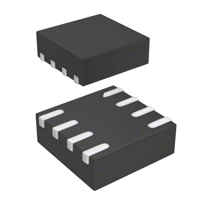
| 产品图片 |
|
| rohs | 符合RoHS无铅 / 符合限制有害物质指令(RoHS)规范要求 |
| 产品系列 | 放大器 IC,运算放大器 - 运放,Texas Instruments LMV722MMX/NOPB- |
| 数据手册 | |
| 产品型号 | LMV722MMX/NOPB |
| PCN设计/规格 | |
| 产品种类 | 运算放大器 - 运放 |
| 供应商器件封装 | 8-VSSOP |
| 共模抑制比—最小值 | 89 dB |
| 关闭 | No Shutdown |
| 其它名称 | 296-35349-1 |
| 包装 | 剪切带 (CT) |
| 压摆率 | 5.25 V/µs |
| 商标 | Texas Instruments |
| 增益带宽生成 | 10 MHz |
| 增益带宽积 | 10MHz |
| 安装类型 | 表面贴装 |
| 安装风格 | SMD/SMT |
| 封装 | Reel |
| 封装/外壳 | 8-TSSOP,8-MSOP(0.118",3.00mm 宽) |
| 封装/箱体 | VSSOP-8 |
| 工作温度 | -40°C ~ 85°C |
| 工作电源电压 | 3 V, 5 V |
| 工厂包装数量 | 3500 |
| 放大器类型 | 通用 |
| 最大工作温度 | + 85 C |
| 最小工作温度 | - 40 C |
| 标准包装 | 1 |
| 电压-电源,单/双 (±) | 2.2 V ~ 5.5 V, ±1.1 V ~ 2.25 V |
| 电压-输入失调 | 80µV |
| 电流-电源 | 2.01mA |
| 电流-输入偏置 | 260nA |
| 电流-输出/通道 | 52.6mA |
| 电源电流 | 2.01 mA |
| 电路数 | 2 |
| 系列 | LMV722-N |
| 转换速度 | 5.25 V/us |
| 输入偏压电流—最大 | 260 nA |
| 输入补偿电压 | 3 mV |
| 输出电流 | 52.6 mA |
| 输出类型 | 满摆幅 |
| 通道数量 | 2 Channel |


- 商务部:美国ITC正式对集成电路等产品启动337调查
- 曝三星4nm工艺存在良率问题 高通将骁龙8 Gen1或转产台积电
- 太阳诱电将投资9.5亿元在常州建新厂生产MLCC 预计2023年完工
- 英特尔发布欧洲新工厂建设计划 深化IDM 2.0 战略
- 台积电先进制程称霸业界 有大客户加持明年业绩稳了
- 达到5530亿美元!SIA预计今年全球半导体销售额将创下新高
- 英特尔拟将自动驾驶子公司Mobileye上市 估值或超500亿美元
- 三星加码芯片和SET,合并消费电子和移动部门,撤换高东真等 CEO
- 三星电子宣布重大人事变动 还合并消费电子和移动部门
- 海关总署:前11个月进口集成电路产品价值2.52万亿元 增长14.8%


PDF Datasheet 数据手册内容提取
LMV721-N, LMV722-N www.ti.com SNOS414I–AUGUST1999–REVISEDAUGUST2013 LMV721-N/LMV722 10MHz, Low Noise, Low Voltage, and Low Power Operational Amplifier CheckforSamples:LMV721-N,LMV722-N FEATURES DESCRIPTION 1 • (ForTypical,5VSupplyValues;Unless The LMV721-N (Single) and LMV722 (Dual) are low 2 noise, low voltage, and low power op amps, that can OtherwiseNoted) be designed into a wide range of applications. The • Ensured2.2Vand5.0VPerformance LMV721-N/LMV722 has a unity gain bandwidth of • LowSupplyCurrentLMV721-N/2 10MHz, a slew rate of 5V/us, and a quiescent current 930µA/Amplifierat2.2V of930uA/amplifierat2.2V. • HighUnity-GainBandwidth10MHz The LMV721-N/722 are designed to provide optimal • Rail-to-RailOutputSwing performance in low voltage and low noise systems. They provide rail-to-rail output swing into heavy – at600Ω Load 120mVfromEitherRailat loads. The input common-mode voltage range 2.2V includes ground, and the maximum input offset – at2kΩ Load 50mVfromEitherRailat2.2V voltage are 3.5mV (Over Temp) for the LMV721- • InputCommonModeVoltageRangeIncludes N/LMV722. Their capacitive load capability is also Ground good at low supply voltages. The operating range is from2.2Vto5.5V. • SiliconDust,SC70-5Package2.0x2.0x1.0mm The chip is built with TI's advanced Submicron • InputVoltageNoise9nV/√Hzatf=1KHz Silicon-Gate BiCMOS process. The single version, LMV721-N, is available in 5 pin SOT-23 and a SC70 APPLICATIONS (new) package. The dual version, LMV722, is • CellularanCordlessPhones availableinanSOIC-8andVSSOP-8package. • ActiveFilterandBuffers • LaptopsandPDAs • BatteryPoweredElectronics Typical Application Figure1. ABatteryPoweredMicrophonePreamplifier Thesedeviceshavelimitedbuilt-inESDprotection.Theleadsshouldbeshortedtogetherorthedeviceplacedinconductivefoam duringstorageorhandlingtopreventelectrostaticdamagetotheMOSgates. 1 Pleasebeawarethatanimportantnoticeconcerningavailability,standardwarranty,anduseincriticalapplicationsof TexasInstrumentssemiconductorproductsanddisclaimerstheretoappearsattheendofthisdatasheet. Alltrademarksarethepropertyoftheirrespectiveowners. 2 PRODUCTIONDATAinformationiscurrentasofpublicationdate. Copyright©1999–2013,TexasInstrumentsIncorporated Products conform to specifications per the terms of the Texas Instruments standard warranty. Production processing does not necessarilyincludetestingofallparameters.
LMV721-N, LMV722-N SNOS414I–AUGUST1999–REVISEDAUGUST2013 www.ti.com Absolute Maximum Ratings (1)(2) ESDTolerance (3) HumanBodyModel 2000V MachineModel 100V DifferentialInputVoltage ±SupplyVoltage SupplyVoltage(V+–V−) 6V SolderingInformation InfraredorConvection(20sec.) 235°C StorageTemp.Range −65°Cto150°C JunctionTemperature (4) 150°C (1) AbsoluteMaximumRatingsindicatelimitsbeyondwhichdamagetothedevicemayoccur.OperatingRatingsindicateconditionsfor whichthedeviceisintendedtobefunctional,butspecificperformanceisnotensured.Forensuredspecificationsandthetest conditions,seetheElectricalCharacteristics. (2) IfMilitary/Aerospacespecifieddevicesarerequired,pleasecontacttheTexasInstrumentsSalesOffice/Distributorsforavailabilityand specifications. (3) Humanbodymodel,1.5kΩinserieswith100pF.Machinemodel,200Ωinserieswith100pF. (4) ThemaximumpowerdissipationisafunctionofT ,θ ,andT .Themaximumallowablepowerdissipationatanyambient J(max) JA A temperatureisP =(T –T )/θ .AllnumbersapplyforpackagessoldereddirectlyintoaPCboard. D J(max) A JA Operating Ratings (1) SupplyVoltage 2.2Vto5.5V TemperatureRange −40°C≤T ≤85°C J ThermalResistance(θ ) JA SiliconDustSC70-5Pkg 440°C/W TinySOT-23package 265°C/W SOICpackage,8-pinSurfaceMount 190°C/W VSSOPpackage,8-PinMiniSurfaceMount 235°C/W SOICpackage,14-PinSurfaceMount 145°C/W (1) Appliestobothsingle-supplyandsplit-supplyoperation.Continuousshortcircuitoperationatelevatedambienttemperaturecanresultin exceedingthemaximumallowedjunctiontemperatureof150°C.Outputcurrentsinexcessof30mAoverlongtermmayadversely affectreliability. 2.2V DC Electrical Characteristics Unlessotherwisespecified,alllimitsspecifiedforT =25°C.V+=2.2V,V−=0V,V =V+/2,V =V+/2andR >1MΩ. J CM O L Boldfacelimitsapplyatthetemperatureextremes. Parameter TestConditions Typ (1) Limit (2) Units V InputOffsetVoltage 0.02 3 mV OS 3.5 max TCV InputOffsetVoltageAverageDrift 0.6 μV/°C OS I InputBiasCurrent 260 nA B I InputOffsetCurrent 25 nA OS CMRR CommonModeRejectionRatio 0V≤V ≤1.3V 88 70 dB CM 64 min PSRR PowerSupplyRejectionRatio 2.2V≤V+≤5V,V =0V =0 90 70 dB O CM 64 min V InputCommon-ModeVoltageRange ForCMRR≥50dB −0.30 V CM 1.3 V A LargeSignalVoltageGain R =600Ω 81 75 dB V L V =0.75Vto2.00V 60 min O R =2kΩ 84 75 dB L V =0.50Vto2.10V 60 min O (1) TypicalValuesrepresentthemostlikelyparametricnorm. (2) Alllimitsarespecifiedbytestingorstatisticalanalysis. 2 SubmitDocumentationFeedback Copyright©1999–2013,TexasInstrumentsIncorporated ProductFolderLinks:LMV721-N LMV722-N
LMV721-N, LMV722-N www.ti.com SNOS414I–AUGUST1999–REVISEDAUGUST2013 2.2V DC Electrical Characteristics (continued) Unlessotherwisespecified,alllimitsspecifiedforT =25°C.V+=2.2V,V−=0V,V =V+/2,V =V+/2andR >1MΩ. J CM O L Boldfacelimitsapplyatthetemperatureextremes. Parameter TestConditions Typ (1) Limit (2) Units V OutputSwing R =600ΩtoV+/2 2.125 2.090 V O L 2.065 min 0.071 0.120 V 0.145 max R =2kΩtoV+/2 2.177 2.150 V L 2.125 min 0.056 0.080 V 0.105 max I OutputCurrent Sourcing,V =0V 14.9 10.0 mA O O V (diff)=±0.5V 5.0 min IN Sinking,V =2.2V 17.6 10.0 mA O V (diff)=±0.5V 5.0 min IN I SupplyCurrent LMV721-N 0.93 1.2 S 1.5 mA LMV722 1.81 2.2 max 2.6 2.2V AC Electrical Characteristics Unlessotherwisespecified,alllimitsspecifiedforT =25°C.V+=2.2V,V−=0V,V =V+/2,V =V+/2andR >1 J CM O L MΩ.Boldfacelimitsapplyatthetemperatureextremes. Parameter TestConditions Typ (1) Units SR SlewRate (2) 4.9 V/μs GBW Gain-BandwidthProduct 10 MHz Φ PhaseMargin 67.4 Deg m G GainMargin −9.8 dB m e Input-ReferredVoltageNoise f=1kHz 9 nV/√Hz n i Input-ReferredCurrentNoise f=1kHz 0.3 pA/√Hz n THD TotalHarmonicDistortion f=1kHzA =1 V 0.004 % R =600Ω,V =500mV L O PP (1) TypicalValuesrepresentthemostlikelyparametricnorm. (2) Connectedasvoltagefollowerwith1Vstepinput.Numberspecifiedistheslowerofthepositiveandnegativeslewrate. 5V DC Electrical Characteristics Unlessotherwisespecified,alllimitsspecifiedforT =25°C.V+=5V,V−=0V,V =V+/2,V =V+/2andR >1MΩ. J CM O L Boldfacelimitsapplyatthetemperatureextremes. Parameter TestConditions Typ (1) Limit (2) Units V InputOffsetVoltage −0.08 3 mV OS 3.5 max TCV InputOffsetVoltageAverageDrift 0.6 μV/°C OS I InputBiasCurrent 260 nA B I InputOffsetCurrent 25 nA OS CMRR CommonModeRejectionRatio 0V≤V ≤4.1V 89 70 dB CM 64 min PSRR PowerSupplyRejectionRatio 2.2V≤V+≤5.0V,V =0V =0 90 70 dB O CM 64 min V InputCommon-ModeVoltageRange ForCMRR≥50dB −0.30 V CM 4.1 V (1) TypicalValuesrepresentthemostlikelyparametricnorm. (2) Alllimitsarespecifiedbytestingorstatisticalanalysis. Copyright©1999–2013,TexasInstrumentsIncorporated SubmitDocumentationFeedback 3 ProductFolderLinks:LMV721-N LMV722-N
LMV721-N, LMV722-N SNOS414I–AUGUST1999–REVISEDAUGUST2013 www.ti.com 5V DC Electrical Characteristics (continued) Unlessotherwisespecified,alllimitsspecifiedforT =25°C.V+=5V,V−=0V,V =V+/2,V =V+/2andR >1MΩ. J CM O L Boldfacelimitsapplyatthetemperatureextremes. Parameter TestConditions Typ (1) Limit (2) Units A LargeSignalVoltageGain R =600Ω 87 80 dB V L V =0.75Vto4.80V 70 min O R =2kΩ, 94 85 dB L V =0.70Vto4.90V, 70 min O V OutputSwing R =600ΩtoV+/2 4.882 4.840 V O L 4.815 min 0.134 0.190 V 0.215 max R =2kΩtoV+/2 4.952 4.930 V L 4.905 min 0.076 0.110 V 0.135 max I OutputCurrent Sourcing,V =0V 52.6 25.0 mA O O V (diff)=±0.5V 12.0 min IN Sinking,V =5V 23.7 15.0 mA O V (diff)=±0.5V 8.5 min IN I SupplyCurrent LMV721-N 1.03 1.4 S 1.7 mA LMV722 2.01 2.4 max 2.8 5V AC Electrical Characteristics Unlessotherwisespecified,alllimitsspecifiedforT =25°C.V+=5V,V−=0V,V =V+/2,V =V+/2andR >1MΩ. J CM O L Boldfacelimitsapplyatthetemperatureextremes. Parameter TestConditions Typ (1) Units SR SlewRate (2) 5.25 V/μs GBW Gain-BandwidthProduct 10.0 MHz Φ PhaseMargin 72 Deg m G GainMargin −11 dB m e Input-RelatedVoltageNoise f=1kHz 8.5 nV/√Hz n i Input-ReferredCurrentNoise f=1kHz 0.2 pa/√Hz n THD TotalHarmonicDistortion f=1kHz,A =1 V 0.001 % R =600Ω,V =1V L O PP (1) TypicalValuesrepresentthemostlikelyparametricnorm. (2) Connectedasvoltagefollowerwith1Vstepinput.Numberspecifiedistheslowerofthepositiveandnegativeslewrate. 4 SubmitDocumentationFeedback Copyright©1999–2013,TexasInstrumentsIncorporated ProductFolderLinks:LMV721-N LMV722-N
LMV721-N, LMV722-N www.ti.com SNOS414I–AUGUST1999–REVISEDAUGUST2013 Typical Performance Characteristics SupplyCurrent SourcingCurrent vs. vs. SupplyVoltage(LMV721-N) OutputVoltage(V =2.2V) S Figure2. Figure3. SinkingCurrent SourcingCurrentvs. vs. OutputVoltage(V =5V) OutputVoltage(V =2.2V) S S Figure4. Figure5. SinkingCurrent OutputVoltageSwing vs. vs. OutputVoltage(V =5V) SupplyVoltage(R =600Ω) S L Figure6. Figure7. Copyright©1999–2013,TexasInstrumentsIncorporated SubmitDocumentationFeedback 5 ProductFolderLinks:LMV721-N LMV722-N
LMV721-N, LMV722-N SNOS414I–AUGUST1999–REVISEDAUGUST2013 www.ti.com Typical Performance Characteristics (continued) OutputVoltageSwing vs. InputOffsetVoltage SuppyVoltage vs. (R =2kΩ) InputCommon-ModeVoltageRangeV =2.2V L S Figure8. Figure9. InputOffsetVoltage InputOffsetVoltage vs. vs. SupplyVoltage InputCommon-ModeVoltageRangeV =5V (V =V+/2) S CM Figure10. Figure11. InputVoltage InputVoltage vs. vs. OutputVoltage(V =2.2V,R =2kΩ) OutputVoltage(V =5V,R =2kΩ) S L S L Figure12. Figure13. 6 SubmitDocumentationFeedback Copyright©1999–2013,TexasInstrumentsIncorporated ProductFolderLinks:LMV721-N LMV722-N
LMV721-N, LMV722-N www.ti.com SNOS414I–AUGUST1999–REVISEDAUGUST2013 Typical Performance Characteristics (continued) InputVoltageNoise InputCurrentNoise vs. vs. Frequency Frequency Figure14. Figure15. +PSRR −PSRR vs. vs. Frequency Frequency Figure16. Figure17. GainandPhaseMargin CMRR vs. vs. Frequency Frequency (V =2.2V,R 600Ω) S L Figure18. Figure19. Copyright©1999–2013,TexasInstrumentsIncorporated SubmitDocumentationFeedback 7 ProductFolderLinks:LMV721-N LMV722-N
LMV721-N, LMV722-N SNOS414I–AUGUST1999–REVISEDAUGUST2013 www.ti.com Typical Performance Characteristics (continued) GainandPhaseMargin vs. SlewRate Frequency vs. (V =5V,R 600Ω) SupplyVoltage S L Figure20. Figure21. THD vs. Frequency Figure22. 8 SubmitDocumentationFeedback Copyright©1999–2013,TexasInstrumentsIncorporated ProductFolderLinks:LMV721-N LMV722-N
LMV721-N, LMV722-N www.ti.com SNOS414I–AUGUST1999–REVISEDAUGUST2013 APPLICATION NOTES BENEFITS OF THE LMV721-N/722 SIZE The small footprints of the LMV721-N/722 packages save space on printed circuit boards, and enable the design of smaller electronic products, such as cellular phones, pagers, or other portable systems. The low profile of the LMV721-N/722makethempossibletouseinPCMCIAtypeIIIcards. SignalIntegrity Signalscanpickupnoisebetweenthesignalsourceandtheamplifier.Byusingaphysically smalleramplifierpackage,theLMV721-N/722canbeplacedclosertothesignalsource,reducingnoise pickupandincreasingsignalintegrity. SimplifiedBoardLayout Theseproductshelpyoutoavoidusinglongpctracesinyourpcboardlayout.This meansthatnoadditionalcomponents,suchascapacitorsandresistors,areneededtofilteroutthe unwantedsignalsduetotheinterferencebetweenthelongpctraces. LowSupplyCurrentThesedeviceswillhelpyoutomaximizebatterylife.Theyareidealforbatterypowered systems. LowSupplyVoltage TIprovidesensuredperformanceat2.2Vand5V.Thesespecificationsensureoperation throughoutthebatterylifetime. Rail-to-RailOutput Rail-to-railoutputswingprovidesmaximumpossibledynamicrangeattheoutput.Thisis particularlyimportantwhenoperatingonlowsupplyvoltages. InputIncludesGround AllowsdirectsensingnearGNDinsinglesupplyoperation. Protection should be provided to prevent the input voltages from going negative more than −0.3V (at 25°C). An inputclampdiodewitharesistortotheICinputterminalcanbeused. CAPACITIVE LOAD TOLERANCE The LMV721-N/722 can directly drive 4700pF in unity-gain without oscillation. The unity-gain follower is the most sensitive configuration to capacitive loading. Direct capacitive loading reduces the phase margin of amplifiers. The combination of the amplifier's output impedance and the capacitive load induces phase lag. This results in either an underdamped pulse response or oscillation. To drive a heavier capacitive load, circuit in Figure 23 can beused. Figure23. IndirectlyDrivingAcapacitiveLoadUsingResistiveIsolation In Figure 23, the isolation resistor R and the load capacitor C form a pole to increase stability by adding more ISO L phase margin to the overall system. the desired performance depends on the value of R . The bigger the R ISO ISO resistor value, the more stable V will be. Figure 24 is an output waveform of Figure 23 using 100kΩ for R OUT ISO and2000µFforC . L Copyright©1999–2013,TexasInstrumentsIncorporated SubmitDocumentationFeedback 9 ProductFolderLinks:LMV721-N LMV722-N
LMV721-N, LMV722-N SNOS414I–AUGUST1999–REVISEDAUGUST2013 www.ti.com Figure24. PulseResponseoftheLMV721-NCircuitinFigure23 The circuit in Figure 25 is an improvement to the one in Figure 23 because it provides DC accuracy as well as AC stability. If there were a load resistor in Figure 23, the output would be voltage divided by R and the load ISO resistor. Instead, in Figure 25, R provides the DC accuracy by using feed-forward techniques to connect V to F IN R . Caution is needed in choosing the value of R due to the input bias current of the LMV721-N/722. C and L F F R serve to counteract the loss of phase margin by feeding the high frequency component of the output signal ISO back to the amplifier's inverting input, thereby preserving phase margin in the overall feedback loop. Increased capacitivedriveispossiblebyincreasingthevalueofC .Thisinturnwillslowdownthepulseresponse. F Figure25. IndirectlyDrivingACapacitiveLoadwithDCAccuracy INPUT BIAS CURRENT CANCELLATION The LMV721-N/722 family has a bipolar input stage. The typical input bias current of LMV721-N/722 is 260nA with 5V supply. Thus a 100kΩ input resistor will cause 26mV of error voltage. By balancing the resistor values at both inverting and non-inverting inputs, the error caused by the amplifier's input bias current will be reduced. The circuitinFigure26showshowtocanceltheerrorcausedbyinputbiascurrent. Figure26. CancellingtheErrorCausedbyInputBiasCurrent 10 SubmitDocumentationFeedback Copyright©1999–2013,TexasInstrumentsIncorporated ProductFolderLinks:LMV721-N LMV722-N
LMV721-N, LMV722-N www.ti.com SNOS414I–AUGUST1999–REVISEDAUGUST2013 TYPICAL SINGLE-SUPPLY APPLICATION CIRCUITS DifferenceAmplifier The difference amplifier allows the subtraction of two voltages or, as a special case, the cancellation of a signal common to two inputs. It is useful as a computational amplifier, in making a differential to single-ended conversionorinrejectingacommonmodesignal. Figure27. DifferenceApplication (1) (2) InstrumentationCircuits The input impendance of the previous difference amplifier is set by the resistor R , R , R and R . To eliminate 1 2 3 4 the problems of low input impendance, one way is to use a voltage follower ahead of each input as shown in the followingtwoinstrumentationamplifiers. Three-op-ampInstrumentationAmplifier TheLMV721-N/722canbeusedtobuildathree-op-ampinstrumentationamplifierasshowninFigure28 Figure28. Three-op-ampInstrumentationAmplifier The first stage of this instrumentation amplifier is a differential-input, differential-output amplifier, with two voltage followers. These two voltage followers assure that the input impedance is over 100MΩ. The gain of this instrumentation amplifier is set by the ratio of R /R . R should equal R and R equal R . Matching of R to R 2 1 3 1 4 2 3 1 and R to R affects the CMRR. For good CMRR over temperature, low drift resistors should be used. Making R 4 2 4 slightly smaller than R and adding a trim pot equal to twice the difference between R and R will allow the 2 2 4 CMRRtobeadjustedforoptimum. Copyright©1999–2013,TexasInstrumentsIncorporated SubmitDocumentationFeedback 11 ProductFolderLinks:LMV721-N LMV722-N
LMV721-N, LMV722-N SNOS414I–AUGUST1999–REVISEDAUGUST2013 www.ti.com Two-op-ampInstrumentationAmplifier A two-op-amp instrumentation amplifier can also be used to make a high-input impedance DC differential amplifier (Figure 29). As in the two-op-amp circuit, this instrumentation amplifier requires precise resistor matchingforgoodCMRR.R shouldequaltoR andR shouldequalR . 4 1 3 2 Figure29. Two-op-ampInstrumentationAmplifier (3) Single-SupplyInvertingAmplifier There may be cases where the input signal going into the amplifier is negative. Because the amplifier is operating in single supply voltage, a voltage divider using R and R is implemented to bias the amplifier so the 3 4 input signal is within the input common-common voltage range of the amplifier. The capacitor C is placed 1 between the inverting input and resistor R to block the DC signal going into the AC signal source, V . The 1 IN valuesofR andC affectthecutofffrequency, fc=½π R C . 1 1 1 1 As a result, the output signal is centered around mid-supply (if the voltage divider provides V+/2 at the non- invertinginput).Theoutputcanswingtobothrails,maximizingthesignal-to-noiseratioinalowvoltagesystem. Figure30. Single-SupplyInvertingAmplifier (4) ActiveFilter SimpleLow-PassActiveFilter The simple low-pass filter is shown in Figure 31. Its low-pass frequency gain (ω → o) is defined by −R /R . This 3 1 allows low-frequency gains other than unity to be obtained. The filter has a −20dB/decade roll-off after its corner frequency fc. R should be chosen equal to the parallel combination of R and R to minimize error due to bias 2 1 3 current.ThefrequencyresponseofthefilterisshowninFigure32. 12 SubmitDocumentationFeedback Copyright©1999–2013,TexasInstrumentsIncorporated ProductFolderLinks:LMV721-N LMV722-N
LMV721-N, LMV722-N www.ti.com SNOS414I–AUGUST1999–REVISEDAUGUST2013 Figure31. SimpleLow-PassActiveFilter (5) Figure32. FrequencyResponseofSimpleLow-passActiveFilterinFigure31 Note that the single-op-amp active filters are used in to the applications that require low quality factor, Q(≤ 10), lowfrequency(≤ 5KHz),andlowgain(≤10),orasmallvaluefortheproductofgaintimesQ(≤ 100).Theopamp should have an open loop voltage gain at the highest frequency of interest at least 50 times larger than the gain of the filter at this frequency. In addition, the selected op amp should have a slew rate that meets the following requirement: SlewRate≥0.5x(ω V )X10−6V/µsec H OPP where • ω isthehighestfrequencyofinterest H • V istheoutputpeak-to-peakvoltage OPP Figure33. ABatteryPoweredMicrophonePreamplifier Copyright©1999–2013,TexasInstrumentsIncorporated SubmitDocumentationFeedback 13 ProductFolderLinks:LMV721-N LMV722-N
LMV721-N, LMV722-N SNOS414I–AUGUST1999–REVISEDAUGUST2013 www.ti.com Here is a LMV721-N used as a microphone preamplifier. Since the LMV721-N is a low noise and low power op amp, it makes it an ideal candidate as a battery powered microphone preamplifier. The LMV721-N is connected in an inverting configuration. Resistors, R = R = 4.7kΩ, sets the reference half way between V = 3V and 1 2 CC ground. Thus, this configures the op amp for single supply use. The gain of the preamplifier, which is 50 (34dB), is set by resistors R = 10kΩ and R = 500kΩ. The gain bandwidth product for the LMV721-N is 10 MHz. This is 3 4 sufficientformostaudioapplicationsincetheaudiorangeistypicallyfrom20Hzto20kHz.AresistorR =5kΩis 5 usedtobiastheelectretmicrophone.CapacitorsC =C =4.7µFplacedattheinputandoutputoftheopampto 1 2 blockouttheDCvoltageoffset. Connection Diagrams TopView TopView Figure34. 5-PinSC70andSOT-23Packages Figure35. 8-PinSOICandVSSOPPackages SeePackageNumbersDCK0005AANDDBV0005A SeePackageNumbersD0008AandDGK0008A 14 SubmitDocumentationFeedback Copyright©1999–2013,TexasInstrumentsIncorporated ProductFolderLinks:LMV721-N LMV722-N
LMV721-N, LMV722-N www.ti.com SNOS414I–AUGUST1999–REVISEDAUGUST2013 REVISION HISTORY ChangesfromRevisionG(March2013)toRevisionH Page • ChangedlayoutofNationalDataSheettoTIformat.......................................................................................................... 14 Copyright©1999–2013,TexasInstrumentsIncorporated SubmitDocumentationFeedback 15 ProductFolderLinks:LMV721-N LMV722-N
PACKAGE OPTION ADDENDUM www.ti.com 6-Feb-2020 PACKAGING INFORMATION Orderable Device Status Package Type Package Pins Package Eco Plan Lead/Ball Finish MSL Peak Temp Op Temp (°C) Device Marking Samples (1) Drawing Qty (2) (6) (3) (4/5) LMV721M5 NRND SOT-23 DBV 5 1000 TBD Call TI Call TI -40 to 85 A30A LMV721M5/NOPB ACTIVE SOT-23 DBV 5 1000 Green (RoHS SN Level-1-260C-UNLIM -40 to 85 A30A & no Sb/Br) LMV721M5X/NOPB ACTIVE SOT-23 DBV 5 3000 Green (RoHS SN Level-1-260C-UNLIM -40 to 85 A30A & no Sb/Br) LMV721M7 NRND SC70 DCK 5 1000 TBD Call TI Call TI -40 to 85 A20 LMV721M7/NOPB ACTIVE SC70 DCK 5 1000 Green (RoHS SN Level-1-260C-UNLIM -40 to 85 A20 & no Sb/Br) LMV721M7X/NOPB ACTIVE SC70 DCK 5 3000 Green (RoHS SN Level-1-260C-UNLIM -40 to 85 A20 & no Sb/Br) LMV722M NRND SOIC D 8 95 TBD Call TI Call TI -40 to 85 LMV 722M LMV722M/NOPB ACTIVE SOIC D 8 95 Green (RoHS SN Level-1-260C-UNLIM -40 to 85 LMV & no Sb/Br) 722M LMV722MM/NOPB ACTIVE VSSOP DGK 8 1000 Green (RoHS SN Level-1-260C-UNLIM -40 to 85 V722 & no Sb/Br) LMV722MMX/NOPB ACTIVE VSSOP DGK 8 3500 Green (RoHS SN Level-1-260C-UNLIM -40 to 85 V722 & no Sb/Br) LMV722MX/NOPB ACTIVE SOIC D 8 2500 Green (RoHS SN Level-1-260C-UNLIM -40 to 85 LMV & no Sb/Br) 722M (1) The marketing status values are defined as follows: ACTIVE: Product device recommended for new designs. LIFEBUY: TI has announced that the device will be discontinued, and a lifetime-buy period is in effect. NRND: Not recommended for new designs. Device is in production to support existing customers, but TI does not recommend using this part in a new design. PREVIEW: Device has been announced but is not in production. Samples may or may not be available. OBSOLETE: TI has discontinued the production of the device. (2) RoHS: TI defines "RoHS" to mean semiconductor products that are compliant with the current EU RoHS requirements for all 10 RoHS substances, including the requirement that RoHS substance do not exceed 0.1% by weight in homogeneous materials. Where designed to be soldered at high temperatures, "RoHS" products are suitable for use in specified lead-free processes. TI may reference these types of products as "Pb-Free". RoHS Exempt: TI defines "RoHS Exempt" to mean products that contain lead but are compliant with EU RoHS pursuant to a specific EU RoHS exemption. Green: TI defines "Green" to mean the content of Chlorine (Cl) and Bromine (Br) based flame retardants meet JS709B low halogen requirements of <=1000ppm threshold. Antimony trioxide based flame retardants must also meet the <=1000ppm threshold requirement. Addendum-Page 1
PACKAGE OPTION ADDENDUM www.ti.com 6-Feb-2020 (3) MSL, Peak Temp. - The Moisture Sensitivity Level rating according to the JEDEC industry standard classifications, and peak solder temperature. (4) There may be additional marking, which relates to the logo, the lot trace code information, or the environmental category on the device. (5) Multiple Device Markings will be inside parentheses. Only one Device Marking contained in parentheses and separated by a "~" will appear on a device. If a line is indented then it is a continuation of the previous line and the two combined represent the entire Device Marking for that device. (6) Lead/Ball Finish - Orderable Devices may have multiple material finish options. Finish options are separated by a vertical ruled line. Lead/Ball Finish values may wrap to two lines if the finish value exceeds the maximum column width. Important Information and Disclaimer:The information provided on this page represents TI's knowledge and belief as of the date that it is provided. TI bases its knowledge and belief on information provided by third parties, and makes no representation or warranty as to the accuracy of such information. Efforts are underway to better integrate information from third parties. TI has taken and continues to take reasonable steps to provide representative and accurate information but may not have conducted destructive testing or chemical analysis on incoming materials and chemicals. TI and TI suppliers consider certain information to be proprietary, and thus CAS numbers and other limited information may not be available for release. In no event shall TI's liability arising out of such information exceed the total purchase price of the TI part(s) at issue in this document sold by TI to Customer on an annual basis. OTHER QUALIFIED VERSIONS OF LMV722-N : •Automotive: LMV722-Q1 NOTE: Qualified Version Definitions: •Automotive - Q100 devices qualified for high-reliability automotive applications targeting zero defects Addendum-Page 2
PACKAGE MATERIALS INFORMATION www.ti.com 29-Sep-2019 TAPE AND REEL INFORMATION *Alldimensionsarenominal Device Package Package Pins SPQ Reel Reel A0 B0 K0 P1 W Pin1 Type Drawing Diameter Width (mm) (mm) (mm) (mm) (mm) Quadrant (mm) W1(mm) LMV721M5 SOT-23 DBV 5 1000 178.0 8.4 3.2 3.2 1.4 4.0 8.0 Q3 LMV721M5/NOPB SOT-23 DBV 5 1000 178.0 8.4 3.2 3.2 1.4 4.0 8.0 Q3 LMV721M5X/NOPB SOT-23 DBV 5 3000 178.0 8.4 3.2 3.2 1.4 4.0 8.0 Q3 LMV721M7 SC70 DCK 5 1000 178.0 8.4 2.25 2.45 1.2 4.0 8.0 Q3 LMV721M7/NOPB SC70 DCK 5 1000 178.0 8.4 2.25 2.45 1.2 4.0 8.0 Q3 LMV721M7X/NOPB SC70 DCK 5 3000 178.0 8.4 2.25 2.45 1.2 4.0 8.0 Q3 LMV722MM/NOPB VSSOP DGK 8 1000 178.0 12.4 5.3 3.4 1.4 8.0 12.0 Q1 LMV722MMX/NOPB VSSOP DGK 8 3500 330.0 12.4 5.3 3.4 1.4 8.0 12.0 Q1 LMV722MX/NOPB SOIC D 8 2500 330.0 12.4 6.5 5.4 2.0 8.0 12.0 Q1 PackMaterials-Page1
PACKAGE MATERIALS INFORMATION www.ti.com 29-Sep-2019 *Alldimensionsarenominal Device PackageType PackageDrawing Pins SPQ Length(mm) Width(mm) Height(mm) LMV721M5 SOT-23 DBV 5 1000 210.0 185.0 35.0 LMV721M5/NOPB SOT-23 DBV 5 1000 210.0 185.0 35.0 LMV721M5X/NOPB SOT-23 DBV 5 3000 210.0 185.0 35.0 LMV721M7 SC70 DCK 5 1000 210.0 185.0 35.0 LMV721M7/NOPB SC70 DCK 5 1000 210.0 185.0 35.0 LMV721M7X/NOPB SC70 DCK 5 3000 210.0 185.0 35.0 LMV722MM/NOPB VSSOP DGK 8 1000 210.0 185.0 35.0 LMV722MMX/NOPB VSSOP DGK 8 3500 367.0 367.0 35.0 LMV722MX/NOPB SOIC D 8 2500 367.0 367.0 35.0 PackMaterials-Page2
None
None
PACKAGE OUTLINE DBV0005A SOT-23 - 1.45 mm max height SCALE 4.000 SMALL OUTLINE TRANSISTOR C 3.0 2.6 0.1 C 1.75 1.45 1.45 B A 0.90 PIN 1 INDEX AREA 1 5 2X 0.95 3.05 2.75 1.9 1.9 2 4 3 0.5 5X 0.3 0.15 0.2 C A B (1.1) TYP 0.00 0.25 GAGE PLANE 0.22 TYP 0.08 8 TYP 0.6 0 0.3 TYP SEATING PLANE 4214839/E 09/2019 NOTES: 1. All linear dimensions are in millimeters. Any dimensions in parenthesis are for reference only. Dimensioning and tolerancing per ASME Y14.5M. 2. This drawing is subject to change without notice. 3. Refernce JEDEC MO-178. 4. Body dimensions do not include mold flash, protrusions, or gate burrs. Mold flash, protrusions, or gate burrs shall not exceed 0.15 mm per side. www.ti.com
EXAMPLE BOARD LAYOUT DBV0005A SOT-23 - 1.45 mm max height SMALL OUTLINE TRANSISTOR PKG 5X (1.1) 1 5 5X (0.6) SYMM (1.9) 2 2X (0.95) 3 4 (R0.05) TYP (2.6) LAND PATTERN EXAMPLE EXPOSED METAL SHOWN SCALE:15X SOLDER MASK SOLDER MASK METAL UNDER METAL OPENING OPENING SOLDER MASK EXPOSED METAL EXPOSED METAL 0.07 MAX 0.07 MIN ARROUND ARROUND NON SOLDER MASK SOLDER MASK DEFINED DEFINED (PREFERRED) SOLDER MASK DETAILS 4214839/E 09/2019 NOTES: (continued) 5. Publication IPC-7351 may have alternate designs. 6. Solder mask tolerances between and around signal pads can vary based on board fabrication site. www.ti.com
EXAMPLE STENCIL DESIGN DBV0005A SOT-23 - 1.45 mm max height SMALL OUTLINE TRANSISTOR PKG 5X (1.1) 1 5 5X (0.6) SYMM 2 (1.9) 2X(0.95) 3 4 (R0.05) TYP (2.6) SOLDER PASTE EXAMPLE BASED ON 0.125 mm THICK STENCIL SCALE:15X 4214839/E 09/2019 NOTES: (continued) 7. Laser cutting apertures with trapezoidal walls and rounded corners may offer better paste release. IPC-7525 may have alternate design recommendations. 8. Board assembly site may have different recommendations for stencil design. www.ti.com
PACKAGE OUTLINE D0008A SOIC - 1.75 mm max height SCALE 2.800 SMALL OUTLINE INTEGRATED CIRCUIT C SEATING PLANE .228-.244 TYP [5.80-6.19] .004 [0.1] C A PIN 1 ID AREA 6X .050 [1.27] 8 1 2X .189-.197 [4.81-5.00] .150 NOTE 3 [3.81] 4X (0 -15 ) 4 5 8X .012-.020 B .150-.157 [0.31-0.51] .069 MAX [3.81-3.98] .010 [0.25] C A B [1.75] NOTE 4 .005-.010 TYP [0.13-0.25] 4X (0 -15 ) SEE DETAIL A .010 [0.25] .004-.010 0 - 8 [0.11-0.25] .016-.050 [0.41-1.27] DETAIL A (.041) TYPICAL [1.04] 4214825/C 02/2019 NOTES: 1. Linear dimensions are in inches [millimeters]. Dimensions in parenthesis are for reference only. Controlling dimensions are in inches. Dimensioning and tolerancing per ASME Y14.5M. 2. This drawing is subject to change without notice. 3. This dimension does not include mold flash, protrusions, or gate burrs. Mold flash, protrusions, or gate burrs shall not exceed .006 [0.15] per side. 4. This dimension does not include interlead flash. 5. Reference JEDEC registration MS-012, variation AA. www.ti.com
EXAMPLE BOARD LAYOUT D0008A SOIC - 1.75 mm max height SMALL OUTLINE INTEGRATED CIRCUIT 8X (.061 ) [1.55] SYMM SEE DETAILS 1 8 8X (.024) [0.6] SYMM (R.002 ) TYP [0.05] 5 4 6X (.050 ) [1.27] (.213) [5.4] LAND PATTERN EXAMPLE EXPOSED METAL SHOWN SCALE:8X SOLDER MASK SOLDER MASK METAL OPENING OPENING METAL UNDER SOLDER MASK EXPOSED METAL EXPOSED METAL .0028 MAX .0028 MIN [0.07] [0.07] ALL AROUND ALL AROUND NON SOLDER MASK SOLDER MASK DEFINED DEFINED SOLDER MASK DETAILS 4214825/C 02/2019 NOTES: (continued) 6. Publication IPC-7351 may have alternate designs. 7. Solder mask tolerances between and around signal pads can vary based on board fabrication site. www.ti.com
EXAMPLE STENCIL DESIGN D0008A SOIC - 1.75 mm max height SMALL OUTLINE INTEGRATED CIRCUIT 8X (.061 ) [1.55] SYMM 1 8 8X (.024) [0.6] SYMM (R.002 ) TYP [0.05] 5 4 6X (.050 ) [1.27] (.213) [5.4] SOLDER PASTE EXAMPLE BASED ON .005 INCH [0.125 MM] THICK STENCIL SCALE:8X 4214825/C 02/2019 NOTES: (continued) 8. Laser cutting apertures with trapezoidal walls and rounded corners may offer better paste release. IPC-7525 may have alternate design recommendations. 9. Board assembly site may have different recommendations for stencil design. www.ti.com
None
None
IMPORTANTNOTICEANDDISCLAIMER TI PROVIDES TECHNICAL AND RELIABILITY DATA (INCLUDING DATASHEETS), DESIGN RESOURCES (INCLUDING REFERENCE DESIGNS), APPLICATION OR OTHER DESIGN ADVICE, WEB TOOLS, SAFETY INFORMATION, AND OTHER RESOURCES “AS IS” AND WITH ALL FAULTS, AND DISCLAIMS ALL WARRANTIES, EXPRESS AND IMPLIED, INCLUDING WITHOUT LIMITATION ANY IMPLIED WARRANTIES OF MERCHANTABILITY, FITNESS FOR A PARTICULAR PURPOSE OR NON-INFRINGEMENT OF THIRD PARTY INTELLECTUAL PROPERTY RIGHTS. These resources are intended for skilled developers designing with TI products. You are solely responsible for (1) selecting the appropriate TI products for your application, (2) designing, validating and testing your application, and (3) ensuring your application meets applicable standards, and any other safety, security, or other requirements. These resources are subject to change without notice. TI grants you permission to use these resources only for development of an application that uses the TI products described in the resource. Other reproduction and display of these resources is prohibited. No license is granted to any other TI intellectual property right or to any third party intellectual property right. TI disclaims responsibility for, and you will fully indemnify TI and its representatives against, any claims, damages, costs, losses, and liabilities arising out of your use of these resources. TI’s products are provided subject to TI’s Terms of Sale (www.ti.com/legal/termsofsale.html) or other applicable terms available either on ti.com or provided in conjunction with such TI products. TI’s provision of these resources does not expand or otherwise alter TI’s applicable warranties or warranty disclaimers for TI products. Mailing Address: Texas Instruments, Post Office Box 655303, Dallas, Texas 75265 Copyright © 2020, Texas Instruments Incorporated