ICGOO在线商城 > 集成电路(IC) > 线性 - 放大器 - 仪表,运算放大器,缓冲器放大器 > MAX4246ASA+

 Datasheet下载
- 型号: MAX4246ASA+
- 制造商: Maxim
- 库位|库存: xxxx|xxxx
- 要求:
| 数量阶梯 | 香港交货 | 国内含税 |
| +xxxx | $xxxx | ¥xxxx |
查看当月历史价格
查看今年历史价格
MAX4246ASA+产品简介:
ICGOO电子元器件商城为您提供MAX4246ASA+由Maxim设计生产,在icgoo商城现货销售,并且可以通过原厂、代理商等渠道进行代购。 MAX4246ASA+价格参考。MaximMAX4246ASA+封装/规格:线性 - 放大器 - 仪表,运算放大器,缓冲器放大器, General Purpose Amplifier 2 Circuit Rail-to-Rail 8-SOIC。您可以下载MAX4246ASA+参考资料、Datasheet数据手册功能说明书,资料中有MAX4246ASA+ 详细功能的应用电路图电压和使用方法及教程。
MAX4246ASA+是Maxim Integrated推出的一款低功耗、高精度运算放大器,属于线性放大器中的精密运算放大器类别。该器件采用单电源供电,具有轨至轨输入和输出(Rail-to-Rail I/O)特性,工作电压范围为1.8V至5.5V,适合低电压便携式设备应用。

典型应用场景包括:便携式医疗设备(如血糖仪、心率监测仪)、工业传感器信号调理、电池供电仪器、数据采集系统以及消费类电子产品中的模拟信号放大与处理。其低失调电压、低温漂和低噪声特性,使其在微弱信号放大场合表现出色,能够确保高精度测量的稳定性。

此外,MAX4246ASA+具备单位增益稳定设计,适用于电压跟随器、有源滤波器、电流检测放大电路等配置。其小尺寸封装(如8-pin SOIC)节省PCB空间,适合对空间要求严格的紧凑型设计。整体而言,该器件广泛应用于需要高精度、低功耗和小型化的模拟前端信号处理领域。
| 参数 | 数值 |
| -3db带宽 | - |
| 产品目录 | 集成电路 (IC)半导体 |
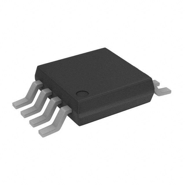
| 描述 | IC OPAMP GP 1MHZ RRO 8SOIC运算放大器 - 运放 Rail-Rail I/O w/Disable |
| 产品分类 | Linear - Amplifiers - Instrumentation, OP Amps, Buffer Amps集成电路 - IC |
| 品牌 | Maxim Integrated |
| 产品手册 | |
| 产品图片 |
|
| rohs | 符合RoHS无铅 / 符合限制有害物质指令(RoHS)规范要求 |
| 产品系列 | 放大器 IC,运算放大器 - 运放,Maxim Integrated MAX4246ASA+- |
| 数据手册 | |
| 产品型号 | MAX4246ASA+ |
| 产品培训模块 | http://www.digikey.cn/PTM/IndividualPTM.page?site=cn&lang=zhs&ptm=25703http://www.digikey.cn/PTM/IndividualPTM.page?site=cn&lang=zhs&ptm=25705 |
| 产品目录页面 | |
| 产品种类 | 运算放大器 - 运放 |
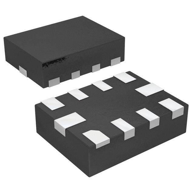
| 供应商器件封装 | 8-SOIC N |
| 共模抑制比—最小值 | 80 dB |
| 关闭 | No Shutdown |
| 其它有关文件 | |
| 包装 | 管件 |
| 压摆率 | 0.4 V/µs |
| 商标 | Maxim Integrated |
| 增益带宽生成 | 1 MHz |
| 增益带宽积 | 1MHz |
| 安装类型 | 表面贴装 |
| 安装风格 | SMD/SMT |
| 封装 | Tube |
| 封装/外壳 | 8-SOIC(0.154",3.90mm 宽) |
| 封装/箱体 | SO-8 |
| 工作温度 | -40°C ~ 125°C |
| 工作电源电压 | 2.5 V to 5.5 V, +/- 1.25 V to +/- 2.75 V |
| 工厂包装数量 | 100 |
| 技术 | BiCMOS |
| 放大器类型 | 通用 |
| 最大双重电源电压 | +/- 2.75 V |
| 最大工作温度 | + 125 C |
| 最小双重电源电压 | +/- 1.25 V |
| 最小工作温度 | - 40 C |
| 标准包装 | 1 |
| 电压-电源,单/双 (±) | 2.5 V ~ 5.5 V, ±1.25 V ~ 2.75 V |
| 电压-输入失调 | 400µV |
| 电流-电源 | 375µA |
| 电流-输入偏置 | 10nA |
| 电流-输出/通道 | 30mA |
| 电源电流 | 320 uA |
| 电路数 | 2 |
| 系列 | MAX4246 |
| 转换速度 | 0.4 V/us |
| 输入偏压电流—最大 | 50 nA |
| 输入参考电压噪声 | 52 nV |
| 输入补偿电压 | 1.5 mV |
| 输出电流 | 30 mA |
| 输出类型 | 满摆幅 |
| 通道数量 | 2 Channel |
| 零件号别名 | MAX4246 |


PDF Datasheet 数据手册内容提取
MAX4245/MAX4246/ Ultra-Small, Rail-to-Rail I/O with Disable, MAX4247 Single-/Dual-Supply, Low-Power Op Amps General Description Features The MAX4245/MAX4246/MAX4247 family of low-cost op ● Rail-to-Rail Input and Output Voltage Swing amps offer rail-to-rail inputs and outputs, draw only 320µA ● 50nA (max) Shutdown Mode (MAX4245/MAX4247) of quiescent current, and operate from a single +2.5V ● 320µA (typ) Quiescent Current Per Amplifier to +5.5V supply. For additional power conservation, the MAX4245/MAX4247 offer a low-power shutdown mode ● Single +2.5V to +5.5V Supply Voltage Range that reduces supply current to 50nA, and puts the ampli- ● 110dB Open-Loop Gain with 2kΩ Load fiers outputs in a high-impedance state. These devices ● 0.01% THD with 100kΩ Load are unity-gain stable with a 1MHz gain-bandwidth prod uct driving capacitive loads up to 470pF. ● Unity-Gain Stable up to CLOAD = 470pF The MAX4245/MAX4246/MAX4247 family is specified ● No Phase Inversion for Overdriven Inputs from -40°C to +125°C, making them suitable for use in ● Available in Space-Saving Packages a variety of harsh environments. The MAX4245 single 6-Pin SC70 or 6-Pin SOT23 (MAX4245) amplifier is available in ultra-small 6-pin SC70 and space- 8-Pin SOT23/SO or 8-Pin µMAX (MAX4246) saving 6-pin SOT23 packages. The MAX4246 dual 10-Pin µMAX (MAX4247) amplifier is available in 8-pin SOT23, SO, and µMAX® packages. The MAX4247 dual amplifier comes in a tiny Ordering Information 10-pin µMAX package. PIN- TOP PART TEMP RANGE Applications PACKAGE MARK ● Portable Communications MAX4245AXT+T -40°C to +125°C 6 SC70 AAZ ● Single-Supply Zero-Crossing Detectors MAX4245AUT+T -40°C to +125°C 6 SOT23 AAUB ● Instruments and Terminals MAX4246AKA+T -40°C to +125°C 8 SOT23 AAIN ● Electronic Ignition Modules MAX4246ASA+T -40°C to +125°C 8 SO — ● Infrared Receivers ● Sensor-Signal Detection MAX4246AUA+T -40°C to +125°C 8 µMAX — MAX4247AUB+T -40°C to +125°C 10 µMAX — +Denotes a lead(Pb)-free/RoHS-compliant package. Selector Guide T = Tape and reel. AMPLIFIERS SHUTDOWN PART PER PACKAGE MODE Pin Configurations MAX4245AXT 1 Yes TOP VIEW MAX4245AUT 1 Yes + + MAX4246AKA 2 No IN+ 1 MAX4245 6 VDD OUTA 1 MAX4246 8 VDD MAX4246ASA 2 No INA- 2 7 OUTB VSS 2 5 SHDN MAX4246AUA 2 No MAX4247AUB 2 Yes IN- 3 4 OUT INA+ 3 6 INB- SC70-6/SOT23-6 VSS 4 5 INB+ SOT23-8/µMAX-8 μMAX is a registered trademark of Maxim Integrated Products, Inc. Pin Configurations continued at end of datat sheet. 19-2016; Rev 3; 5/14
MAX4245/MAX4246/ Ultra-Small, Rail-to-Rail I/O with Disable, MAX4247 Single-/Dual-Supply, Low-Power Op Amps Absolute Maximum Ratings Power-Supply Voltage (VDD to VSS) .......................-0.3V to +6V 8-Pin SOT23 (derate 9.1mW/°C above +70°C) ..........727mW All Other Pins ................................(VSS - 0.3V) to (VDD + 0.3V) 8-Pin µMAX (derate 4.5mW/°C above +70°C) ............362mW Output Short-Circuit Duration 10-Pin µMAX (derate 5.6mW/°C above +70°C) ..........444mW (OUT shorted to VSS or VDD) .............................. Continuous Operating Temperature Range .........................-40°C to +125°C Continuous Power Dissipation (TA = +70°C) Junction Temperature ......................................................+150°C 6-Pin SC70 (derate 3.1mW/°C above +70°C) .............245mW Storage Temperature Range ............................-65°C to +160°C 6-Pin SOT23 (derate 8.7mW/°C above +70°C) ..........695mW Lead Temperature (soldering, 10s) .................................+300°C 8-Pin SO (derate 5.9mW/°C above +70°C) .................471mW Soldering Temperature (reflow) .......................................+260°C Stresses beyond those listed under “Absolute Maximum Ratings” may cause permanent damage to the device. These are stress ratings only, and functional operation of the device at these or any other conditions beyond those indicated in the operational sections of the specifications is not implied. Exposure to absolute maximum rating conditions for extended periods may affect device reliability. Electrical Characteristics (VDD = +2.7V, VSS = 0V, VCM = 0V, VOUT = VDD/2, RL connected from OUT to VDD/2, SHDN_ = VDD (MAX4245/MAX4247 only), TA = +25°C, unless otherwise noted.) (Note 1) PARAMETER SYMBOL CONDITIONS MIN TYP MAX UNITS Supply Voltage Range VDD Inferred from PSRR test 2.5 5.5 V VDD = +2.7V 320 650 Supply Current (Per Amplifier) IDD µA VDD = +5.5V 375 700 Supply Current in Shutdown ISHDN_ SHDN_ = VSS (Note 2) 0.05 0.5 µA Input Offset Voltage VOS VSS - 0.1V ≤ VCM ≤ VDD + 0.1V ±0.4 ±1.5 mV Input Bias Current IB VSS - 0.1V ≤ VCM ≤ VDD + 0.1V ±10 ±50 nA Input Offset Current IOS VSS - 0.1V ≤ VCM ≤ VDD + 0.1V ±1 ±6 nA Input Resistance RIN |VIN+ - VIN-| ≤ 10mV 4000 kΩ Input Common-Mode Voltage Range VCM Inferred from CMRR test VSS - 0.1 VDD + 0.1 V Common-Mode Rejection Ratio CMRR VSS - 0.1V ≤ VCM ≤ VDD + 0.1V 65 80 dB Power-Supply Rejection Ratio PSRR 2.5V ≤ VDD ≤ 5.5V 75 90 dB VSS + 0.05V ≤ VOUT ≤ VDD - 0.05V, 120 RL = 100kΩ Large-Signal Voltage Gain AV dB VSS + 0.2V ≤ VOUT ≤ VDD - 0.2V, 95 110 RL = 2kΩ Output Voltage Swing High VOH SVpDeDc -ifi VeOd UaTs RRLL == 120kΩ0kΩ 315 60 mV Output Voltage Swing Low VOL SVpOeUcTifi -e VdS aSs RRLL == 120kΩ0kΩ 310 60 mV Sourcing 11 Output Short-Circuit Current IOUT(SC) VDD = +5.0V mA Sinking 30 Device in Shutdown Mode Output Leakage Current in Shutdown IOUT(SH) (SHDN_ = VSS), VSS ≤ VOUT ≤ VDD ±0.01 ±0.5 µA (Note 2) SHDN_ Logic Low VIL (Note 2) 0.3 x VDD V SHDN_ Logic High VIH (Note 2) 0.7 x VDD V SHDN_ Input Current IL/IH VSS ≤ SHDN_ ≤ VDD (Note 2) 0.5 50 nA www.maximintegrated.com Maxim Integrated │ 2
MAX4245/MAX4246/ Ultra-Small, Rail-to-Rail I/O with Disable, MAX4247 Single-/Dual-Supply, Low-Power Op Amps Electrical Characteristics (continued) (VDD = +2.7V, VSS = 0V, VCM = 0V, VOUT = VDD/2, RL connected from OUT to VDD/2, SHDN_ = VDD (MAX4245/MAX4247 only), TA = +25°C, unless otherwise noted.) (Note 1) PARAMETER SYMBOL CONDITIONS MIN TYP MAX UNITS Gain-Bandwidth Product GBW 1.0 MHz Phase Margin ΦM 70 degrees Gain Margin GM 20 dB Slew Rate SR 0.4 V/µs Input Voltage-Noise Density en f = 10kHz 52 nV/√Hz Input Current-Noise Density in f = 10kHz 0.1 pA/√Hz Capacitive-Load Stability CLOAD AV = 1 (Note 3) 470 pF Shutdown Delay Time t(SH) (Note 2) 3 µs Enable Delay Time t(EN) (Note 2) 4 µs Power-On Time tON 4 µs Input Capacitance CIN 2.5 pF Total Harmonic Distortion THD f = 10kHz, VOUT = 2VP-P, AV = +1, 0.01 % VDD = +5.0V, Load = 100kΩ to VDD/2 Settling Time to 0.01% tS VOUT = 4V step, VDD = +5.0V, AV = +1 10 µs Electrical Characteristics (VDD = +2.7V, VSS = 0V, VCM = 0V, VOUT = VDD/2, RL connected from OUT to VDD/2, SHDN_ = VDD (MAX4245/MAX4247 only), TA = -40°C to +125°C, unless otherwise noted.) (Note 1) PARAMETER SYMBOL CONDITIONS MIN TYP MAX UNITS Supply Voltage Range VDD Inferred from PSRR test 2.5 5.5 V Supply Current (Per Amplifier) IDD VDD = +2.7V 800 µA Supply Current in Shutdown ISHDN_ SHDN_ = VSS (Note 2) 1 µA Input Offset Voltage VOS VSS ≤ VCM ≤ VDD (Note 4) ±3.0 mV Input Offset Voltage Drift TCVOS VSS ≤ VCM ≤ VDD (Note 4) ±2 µV/°C Input Bias Current IB VSS ≤ VCM ≤ VDD (Note 4) ±100 nA Input Offset Current IOS VSS ≤ VCM ≤ VDD (Note 4) ±10 nA Input Common-Mode Voltage Range VCM Inferred from CMRR test (Note 4) VSS VDD V Common-Mode Rejection Ratio CMRR VSS ≤ VCM ≤ VDD (Note 4) 60 dB Power-Supply Rejection Ratio PSRR 2.5V ≤ VDD ≤ 5.5V 70 dB Large-Signal Voltage Gain AV VRSL S= +2 k0Ω.2V ≤ VOUT ≤ VDD - 0.2V, 85 dB Output Voltage Swing High VOH Specified as VDD - VOUT, RL = 2kΩ 90 mV Output Voltage Swing Low VOL Specified as VOUT - VSS, RL = 2kΩ 90 mV Output Leakage Current in IOUT Device in Shutdown Mode (SHDN_ = VSS), ±1.0 µA Shutdown (SH) VSS ≤ VOUT ≤ VDD (Note 3) www.maximintegrated.com Maxim Integrated │ 3
MAX4245/MAX4246/ Ultra-Small, Rail-to-Rail I/O with Disable, MAX4247 Single-/Dual-Supply, Low-Power Op Amps Electrical Characteristics (continued) (VDD = +2.7V, VSS = 0V, VCM = 0V, VOUT = VDD/2, RL connected from OUT to VDD/2, SHDN_ = VDD (MAX4245/MAX4247 only), TA = +25°C, unless otherwise noted.) (Note 1) PARAMETER SYMBOL CONDITIONS MIN TYP MAX UNITS SHDN_ Logic Low VIL (Note 2) 0.3 x VDD V SHDN_ Logic High VIH (Note 2) 0.7 x VDD V SHDN_ Input Current IL/IH VSS ≤ SHDN_ ≤ VDD (Notes 2, 3) 100 nA Note 1: Specifications are 100% tested at TA = +25°C. All temperature limits are guaranteed by design. Note 2: Shutdown mode is only available in MAX4245 and MAX4247. Note 3: Guaranteed by design, not production tested. Note 4: For -40°C to +85°C, Input Common-Mode Range is VSS - 0.1V ≤ VCM ≤ VDD + 0.1V. Typical Operating Characteristics (VDD = 2.7V, VSS = VCM = 0V, VOUT = VDD/2, no load, TA = +25°C, unless otherwise noted.) MAX4245/MAX4247 SUPPLY CURRENT PER AMPLIFIER SHUTDOWN SUPPLY CURRENT INPUT OFFSET VOLTAGE vs. SUPPLY VOLTAGE PER AMPLIFIER vs. TEMPERATURE vs. COMMON-MODE VOLTAGE 455000 TA = +125°C MAX4245 toc01 126000 MAX4245 toc02 560000 VDD = 2.5V TA = +125°C MAX4245 toc03 TA = +85°C 400 400 I (µA)DD350 TTA A= = + +852°5C°C (nA)SHDN120 V (µV)OS 300 TA = +25°C I 80 300 200 TA = -40°C TA = -40°C 40 250 100 200 0 0 2.0 2.5 3.0 3.5 4.0 4.5 5.0 5.5 -40 15 70 125 0 0.5 1.0 1.5 2.0 2.5 VDD (V) TEMPERATURE (°C) VCM (V) INPUT OFFSET VOLTAGE INPUT OFFSET VOLTAGE INPUT BIAS CURRENT vs. COMMON-MODE VOLTAGE vs. TEMPERATURE vs. COMMON-MODE VOLTAGE 560000 VDD = 5.5V TA = +125°C MAX4245 toc04 330500 MAX4245 toc05 1250 VDD = 5.5V TA = -40°C MAX4245 toc06 400 TA = +85°C 250 VDD = 2.5V 10 V (mV)OS 300 TA = +25°C V (µV)OS210500 I (nA)BIAS 50 TA = +1T2A5 =° C+85°C 200 TA = -40°C 100 VDD = 5.5V -5 100 50 -10 TA = +25°C 0 0 -15 0 1 2 3 4 5 6 -40 15 70 125 0 1 2 3 4 5 6 VCM (V) TEMPERATURE (°C) VCM (V) www.maximintegrated.com Maxim Integrated │ 4
MAX4245/MAX4246/ Ultra-Small, Rail-to-Rail I/O with Disable, MAX4247 Single-/Dual-Supply, Low-Power Op Amps Typical Operating Characteristics (VDD = 2.7V, VSS = VCM = 0V, VOUT = VDD/2, no load, TA = +25°C, unless otherwise noted.) OUTPUT SOURCE CURRENT OUTPUT SINK CURRENT OUTPUT SWING HIGH vs. OUTPUT VOLTAGE vs. OUTPUT VOLTAGE vs. TEMPERATURE 1124 VDD = 5.5V MAX4245 toc07 445500 MAX4245 toc08 40 MAX4245 toc09 I (mA)SOURCE 1860 VDD = 2.5V I (mA)SINK 22335005 VDVDD D= =2 .55.V5V V - V (mV)DDOUT 3200 RL = 2kΩ 4 15 10 10 RL = 100kΩ 2 5 0 0 0 0 0.5 1.0 1.5 2.0 2.5 3.0 3.5 4.0 4.5 5.0 5.5 0 0.5 1.0 1.5 2.0 2.5 3.0 3.5 4.0 4.5 5.0 5.5 -40 15 70 125 VOUT (V) VOUT (V) TEMPERATURE (°C) OUTPUT SWING LOW POWER-SUPPLY REJECTION RATIO vs. TEMPERATURE CROSSTALK vs. FREQUENCY vs. FREQUENCY 40 MAX4245 toc10 -50 MAX4245 toc11 --21000 MAX4245 toc12 -70 V - V (mV)OUTSS 3200 RL = 2kΩ CROSSTALK (dB) -90 PSRR (dB) ----64530000 -70 10 -110 -80 RL = 100kΩ -90 0 -130 -100 -40 15 70 125 0.001 0.01 0.1 1 10 100 1000 10,000 0.1 10 10 100 1000 10,000 TEMPERATURE (°C) FREQUENCY (kHz) FREQUENCY (kHz) TOTAL HARMONIC DISTORTION TOTAL HARMONIC DISTORTION PLUS NOISE vs. INPUT FREQUENCY PLUS NOISE vs. AMPLITUDE GAIN AND PHASE vs. FREQUENCY 1 VRAVOL U==T 1+ =01 02kVΩP-P MAX4245 toc13 101 fRAINVL === 11+k01H0kzΩ MAX4245 toc14 8600 NO LOAD MAX4245 toc15 9300 0.1 VDD = 5.0V VDD = 5.0V THD + N (%)0.01 THD + N (%)00.0.11 GAIN (dB)4200 GAIN PHASE --3900PHASE (deg) 0 -150 0.001 0.001 -20 -210 0.0001 0.0001 -40 -270 100 1000 10,000 100,000 0 1 2 3 4 5 0.1 1 10 100 1000 10,000 INPUT FREQUENCY (Hz) OUTPUT VOLTAGE (VP-P) FREQUENCY (kHz) www.maximintegrated.com Maxim Integrated │ 5
MAX4245/MAX4246/ Ultra-Small, Rail-to-Rail I/O with Disable, MAX4247 Single-/Dual-Supply, Low-Power Op Amps Typical Operating Characteristics (continued) (VDD = 2.7V, VSS = VCM = 0V, VOUT = VDD/2, no load, TA = +25°C, unless otherwise noted.) SMALL-SIGNAL TRANSIENT GAIN AND PHASE vs. FREQUENCY RESPONSE (NONINVERTING) 80 MAX4245 toc16 90 MAX4245 toc17 2kΩ || 470pF 60 30 20mV/div N (dB)4200 PHASE --3900SE (deg) IN GAI PHA GAIN 0 -150 20mV/div -20 -210 OUT -40 -270 0.1 1 10 100 1000 10,000 4µs/div FREQUENCY (kHz) SMALL-SIGNAL TRANSIENT LARGE-SIGNAL TRANSIENT RESPONSE (INVERTING) RESPONSE (NONINVERTING) MAX4245 toc18 MAX4245 toc19 IN VDD = 5V 20mV/div 2V/div IN 20mV/div 2V/div OUT OUT 4µs/div 40µs/div LARGE-SIGNAL TRANSIENT RESPONSE (INVERTING) MAX4245 toc20 VDD = 5V IN 2V/div 2V/div OUT 40µs/div www.maximintegrated.com Maxim Integrated │ 6
MAX4245/MAX4246/ Ultra-Small, Rail-to-Rail I/O with Disable, MAX4247 Single-/Dual-Supply, Low-Power Op Amps Pin Description PIN NAME FUNCTION MAX4245 MAX4246 MAX4247 1 — — IN+ Noninverting Input 2 4 4 VSS Ground or Negative Supply 3 — — IN- Inverting Input 4 — — OUT Amplifier Output 5 — — SHDN Shutdown 6 8 10 VDD Positive Supply — 1 1 OUTA Amplifier Output Channel A — 2 2 INA- Inverting Input Channel A — 3 3 INA+ Noninverting Input Channel A — 5 7 INB+ Noninverting Input Channel B — 6 8 INB- Inverting Input Channel B — 7 9 OUTB Amplifier Output Channel B — — 5 SHDNA Shutdown Channel A — — 6 SHDNB Shutdown Channel B VDD VDD R3 R3 IN R3 = R1 ║R2 R3 = R1 ║R2 IN R1 R2 R1 R2 Figure 1a. Minimizing Offset Error Due to Input Bias Current Figure 1b. Minimizing Offset Error Due to Input Bias Current (Noninverting) (Inverting) Detailed Description Since the input stage consists of NPN and PNP pairs, the input bias current changes polarity as the common-mode Rail-to-Rail Input Stage voltage passes through the crossover region. Match the The MAX4245/MAX4246/MAX4247 have rail-to-rail input effective impedance seen by each input to reduce the and output stages that are specifically designed for low- offset error caused by input bias currents flowing through voltage, single-supply operation. The input stage consists external source impedance (Figures 1a and 1b). of composite NPN and PNP differential stages, which The combination of high-source impedance plus input operate together to provide a common-mode range capacitance (amplifier input capacitance plus stray capac- extending to both supply rails. The crossover region itance) creates a parasitic pole that can produce an of these two pairs occurs halfway between VDD and underdamped signal response. Reducing input capaci- VSS. The input offset voltage is typically ±400µV. Low- tance or placing a small capacitor across the feedback operating supply voltage, low supply current and rail-to- resistor improves response in this case. rail outputs make this family of operational amplifiers an excellent choice for precision or general-purpose, low- The MAX4245/MAX4246/MAX4247 family’s inputs are voltage, battery-powered systems. protected from large differential input voltages by internal 5.3kΩ series resistors and back-to-back triple-diode stacks across the inputs (Figure 2). For differential-input voltages www.maximintegrated.com Maxim Integrated │ 7
MAX4245/MAX4246/ Ultra-Small, Rail-to-Rail I/O with Disable, MAX4247 Single-/Dual-Supply, Low-Power Op Amps 5.3kΩ IN- IN 2V/div IN+ 5.3kΩ OUT 2V/div Figure 2. Input Protection Circuit much less than 2.1V (triple-diode drop), input resistance is 400µs/div typically 4MΩ. For differential voltages greater than 2.1V, input resistance is around 10.6kΩ, and the input bias cur- Figure 3. Rail-to-Rail Input/Output Voltage Range rent can be approximated by the following equation: IB = (VDIFF - 2.1V)/10.6kΩ In the region where the differential input voltage approach- es 2.1V, the input resistance decreases exponentially from 4MΩ to 10.6kΩ as the diodes begin to conduct. It fol- 2V/div lows that the bias current increases with the same curve. In unity-gain configuration, high slew-rate input signals VDD may capacitively couple to the output through the triple- diode stacks. Rail-to-Rail Output Stage 2V/div The MAX4245/MAX4246/MAX4247 can drive a 2kΩ load and still typically swing within 35mV of the supply rails. OUT Figure 3 shows the output voltage swing of the MAX4245 configured with AV = -1V/V. 10µs/div Applications Information Figure 4. Power-Up/Power-Down Waveform Power-Supply Considerations The MAX4245/MAX4246/MAX4247 operate from a single the output enters a high-impedance state. Pulling SHDN_ +2.5V to +5.5V supply (or dual ±1.25V to ±2.75V sup- high enables the amplifier. Figure 5 shows the MAX4245/ plies) and consume only 320µA of supply current per MAX4247’s shutdown waveform. amplifier. A 90dB power-supply rejection ratio allows the Due to the output leakage currents of three-state devices amplifiers to be powered directly off a decaying battery and the small internal pullup current for SHDN_, do not voltage, simplifying design and extending battery life. leave SHDN_ open/high-impedance. Leaving SHDN_ open may result in indeterminate logic levels, and could Power-Up adversely affect op amp operation. The logic threshold for The MAX4245/MAX4246/MAX4247 output typically set- SHDN_ is referred to VSS. When using dual supplies, pull tles within 4µs after power-up. Figure 4 shows the output SHDN_ to VSS, not GND, to shut down the op amp. voltage on power-up and power-down. Driving Capacitive Loads Shutdown Mode The MAX4245/MAX4246/MAX4247 are unity-gain stable The MAX4245/MAX4247 feature a low-power shutdown for loads up to 470pF. Applications that require greater mode. When SHDN_ is pulled low, the supply current capacitive drive capability should use an isolation resistor drops to 50nA per amplifier, the amplifier is disabled, and www.maximintegrated.com Maxim Integrated │ 8
MAX4245/MAX4246/ Ultra-Small, Rail-to-Rail I/O with Disable, MAX4247 Single-/Dual-Supply, Low-Power Op Amps 2V/div RISO OUT SHDN IN RL CL 2V/div Figure 6a. Using a Resistor to Isolate a Capacitive Load from OUT the Op Amp 400µs/div Figure 5. Shutdown Waveform RISO = 0Ω RL = 2kΩ CL = 2200pF 100mV/div between the output and the capacitive load (Figures 6a, 6b, 6c). Note that this alternative results in a loss of gain accu- IN racy because RISO forms a voltage divider with the RLOAD. Power-Supply Bypassing and Layout The MAX4245/MAX4246/MAX4247 family operates from 100mV/div either a single +2.5V to +5.5V supply or dual ±1.25V to ±2.75V supplies. For single-supply operation, bypass the OUT power supply with a 100nF capacitor to VSS (in this case GND). For dual-supply operation, both the VDD and the 10µs/div VSS supplies should be bypassed to ground with separate 100nF capacitors. Figure 6b. Pulse Response Without Isolating Resistor Good PC board layout techniques optimize performance by decreasing the amount of stray capacitance at the op amp?s inputs and output. To decrease stray capacitance, RISO = 100Ω minimize trace lengths and widths by placing external RL = 2kΩ components as close to the device as possible. Use CL = 2200pF 100mV/div surface-mount components when possible. IN Pin Configurations (continued) TOP VIEW 100mV/div + OUTA 1 10 VDD OUT MAX4247 INA- 2 9 OUTB 10µs/div Figure 6c. Pulse Response With Isolating Resistor INA+ 3 8 INB- VSS 4 7 INB+ Chip Information PROCESS: BiCMOS SHDNA 5 6 SHDNB µMAX www.maximintegrated.com Maxim Integrated │ 9
MAX4245/MAX4246/ Ultra-Small, Rail-to-Rail I/O with Disable, MAX4247 Single-/Dual-Supply, Low-Power Op Amps Package Information For the latest package outline information and land patterns (footprints), go to www.maximintegrated.com/packages. Note that a “+”, “#”, or “-” in the package code indicates RoHS status only. Package drawings may show a different suffix character, but the drawing pertains to the package regardless of RoHS status. PACKAGE TYPE PACKAGE CODE DOCUMENT NO. LAND PATTERN NO. 6 SOT23 U6+4 21-0058 90-0175 6 SC70 X6SN+1 21-0077 90-0189 8 SOT23 K8+5 21-0078 90-0176 8 SO S8+4 21-0041 90-0096 8 µMAX U8+1 21-0036 90-0092 10 µMAX U10+2 21-0061 90-0330 www.maximintegrated.com Maxim Integrated │ 10
MAX4245/MAX4246/ Ultra-Small, Rail-to-Rail I/O with Disable, MAX4247 Single-/Dual-Supply, Low-Power Op Amps Revision History REVISION REVISION PAGES DESCRIPTION NUMBER DATE CHANGED 0 5/01 Initial release — 2 11/11 Added lead-free data to Ordering Information. 1 3 5/14 Updated the General Description. 1 For pricing, delivery, and ordering information, please contact Maxim Direct at 1-888-629-4642, or visit Maxim Integrated’s website at www.maximintegrated.com. Maxim Integrated cannot assume responsibility for use of any circuitry other than circuitry entirely embodied in a Maxim Integrated product. No circuit patent licenses are implied. Maxim Integrated reserves the right to change the circuitry and specifications without notice at any time. The parametric values (min and max limits) shown in the Electrical Characteristics table are guaranteed. Other parametric values quoted in this data sheet are provided for guidance. Maxim Integrated and the Maxim Integrated logo are trademarks of Maxim Integrated Products, Inc. © 2014 Maxim Integrated Products, Inc. │ 11