ICGOO在线商城 > 集成电路(IC) > 线性 - 放大器 - 仪表,运算放大器,缓冲器放大器 > TSX922IQ2T

 Datasheet下载
- 型号: TSX922IQ2T
- 制造商: STMicroelectronics
- 库位|库存: xxxx|xxxx
- 要求:
| 数量阶梯 | 香港交货 | 国内含税 |
| +xxxx | $xxxx | ¥xxxx |
查看当月历史价格
查看今年历史价格
TSX922IQ2T产品简介:
ICGOO电子元器件商城为您提供TSX922IQ2T由STMicroelectronics设计生产,在icgoo商城现货销售,并且可以通过原厂、代理商等渠道进行代购。 TSX922IQ2T价格参考。STMicroelectronicsTSX922IQ2T封装/规格:线性 - 放大器 - 仪表,运算放大器,缓冲器放大器, 通用 放大器 2 电路 满摆幅 8-DFN(2x2)。您可以下载TSX922IQ2T参考资料、Datasheet数据手册功能说明书,资料中有TSX922IQ2T 详细功能的应用电路图电压和使用方法及教程。
STMicroelectronics的TSX922IQ2T是一款双路、低功耗、轨到轨输入/输出运算放大器,属于线性放大器类别。该器件适用于需要高精度信号调理和宽动态范围的应用场景。

典型应用场景包括:

1. 工业自动化与控制系统:用于传感器信号放大、滤波和调理,如压力、温度、流量等模拟信号的处理。

2. 便携式设备与电池供电系统:由于其低功耗特性,适合用于手持仪器、数据采集系统及低功耗传感器接口电路。

3. 医疗电子设备:如心电图仪、血糖仪等便携式诊断设备中的信号放大与处理模块。

4. 消费类电子产品:用于音频前置放大器、传感器接口、触摸屏控制器中的信号处理部分。

5. 汽车电子应用:如车身控制模块、车载传感器信号调节电路等对可靠性和工作温度范围要求较高的环境。

TSX922IQ2T具备宽电源电压范围(2.7V至16V)、低输入偏置电流、高增益带宽积(1MHz)等特点,使其在多种通用和精密模拟电路中具有良好的性能表现。
| 参数 | 数值 |
| -3db带宽 | - |
| 产品目录 | 集成电路 (IC)半导体 |
| 描述 | IC OPAMP R-R 10MHZ 16V CMOS 8DFN运算放大器 - 运放 10MHz, rail-to-rail 16V CMOS op-amps |
| 产品分类 | Linear - Amplifiers - Instrumentation, OP Amps, Buffer Amps集成电路 - IC |
| 品牌 | STMicroelectronics |
| 产品手册 | |
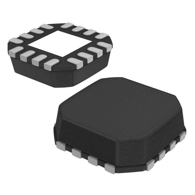
| 产品图片 |
|
| rohs | 符合RoHS无铅 / 符合限制有害物质指令(RoHS)规范要求 |
| 产品系列 | 放大器 IC,运算放大器 - 运放,STMicroelectronics TSX922IQ2T- |
| mouser_ship_limit | 该产品可能需要其他文件才能进口到中国。 |
| 数据手册 | |
| 产品型号 | TSX922IQ2T |
| 产品种类 | 运算放大器 - 运放 |
| 供应商器件封装 | 8-DFN(2x2) |
| 共模抑制比—最小值 | 57 dB |
| 其它名称 | 497-14082-1 |
| 包装 | 剪切带 (CT) |
| 压摆率 | 17 V/µs |
| 商标 | STMicroelectronics |
| 增益带宽生成 | 10 MHz |
| 增益带宽积 | 10MHz |
| 安装类型 | 表面贴装 |
| 安装风格 | SMD/SMT |
| 封装 | Reel |
| 封装/外壳 | 8-WFDFN |
| 封装/箱体 | DFN-8 |
| 工作温度 | -40°C ~ 125°C |
| 工作电源电压 | 4 V to 16 V |
| 工厂包装数量 | 3000 |
| 技术 | CMOS |
| 放大器类型 | 通用 |
| 最大工作温度 | + 125 C |
| 最小工作温度 | - 40 C |
| 标准包装 | 1 |
| 特色产品 | http://www.digikey.com/product-highlights/cn/zh/stmicroelectronics-high-performance-op-amps/4227 |
| 电压-电源,单/双 (±) | 4 V ~ 16 V |
| 电压-输入失调 | 4mV |
| 电流-电源 | 2.8mA |
| 电流-输入偏置 | 10pA |
| 电流-输出/通道 | 74mA |
| 电源电流 | 3.5 mA |
| 电路数 | 2 |
| 系列 | TSX922 |
| 转换速度 | 17 V/us |
| 输入偏压电流—最大 | 200 pA |
| 输入参考电压噪声 | 17.9 nV |
| 输入类型 | Rail to Rail |
| 输入补偿电压 | 5 mV |
| 输出类型 | Rail to Rail |
| 通道数量 | 2 Channel |


- 商务部:美国ITC正式对集成电路等产品启动337调查
- 曝三星4nm工艺存在良率问题 高通将骁龙8 Gen1或转产台积电
- 太阳诱电将投资9.5亿元在常州建新厂生产MLCC 预计2023年完工
- 英特尔发布欧洲新工厂建设计划 深化IDM 2.0 战略
- 台积电先进制程称霸业界 有大客户加持明年业绩稳了
- 达到5530亿美元!SIA预计今年全球半导体销售额将创下新高
- 英特尔拟将自动驾驶子公司Mobileye上市 估值或超500亿美元
- 三星加码芯片和SET,合并消费电子和移动部门,撤换高东真等 CEO
- 三星电子宣布重大人事变动 还合并消费电子和移动部门
- 海关总署:前11个月进口集成电路产品价值2.52万亿元 增长14.8%


PDF Datasheet 数据手册内容提取
TSX920, TSX921, TSX922, TSX923 10 MHz rail-to-rail CMOS 16 V operational amplifiers Datasheet - production data Applications Communications Process control Test equipment Description The TSX92x single and dual operational amplifiers (op amps) offer excellent AC characteristics such as 10 MHz gain bandwidth, 17 V/ms slew rate, and 0.0003 % THD+N. These features make the TSX92x family particularly well-adapted for communications, I/V amplifiers for ADCs, and active filtering applications. Their rail-to-rail input and output capability, while operating on a wide supply voltage range of 4 V to 16 V, allows these devices to be used in a wide range of applications. Automotive qualification is available as these devices can be used in this market segment. Shutdown mode is available on the single Features (TSX920) and dual (TSX923) versions enabling Rail-to-rail input and output an important current consumption reduction while Wide supply voltage: 4 V - 16 V this function is active. Gain bandwidth product: 10 MHz typ at 16 V The TSX92x family is available in SMD packages Low power consumption: 2.8 mA typ per featuring a high level of integration. The DFN8 amplifier at 16 V package, used in the TSX922, with a typical size Unity gain stable of 2x2 mm and a maximum height of 0.8 mm Low input bias current: 10 pA typ offers even greater package size reduction. High tolerance to ESD: 4 kV HBM Table 1: Device summary Extended temperature range: -40 °C to 125 °C Op-amp With shutdown Without Automotive qualification version mode shutdown mode Single TSX920 TSX921 Related products Dual TSX923 TSX922 See the TSX5 series for low-power features See the TSX6 series for micro-power features See the TSX929 series for higher speeds See the TSV9 series for lower voltages January 2016 DocID024310 Rev 4 1/32 This is information on a product in full production. www.st.com
Contents TSX920, TSX921, TSX922, TSX923 Contents 1 Package pin connections ................................................................ 3 2 Absolute maximum ratings and operating conditions ................. 4 3 Electrical characteristics ................................................................ 5 4 Electrical characteristic curves .................................................... 11 5 Application information ................................................................ 17 5.1 Operating voltages .......................................................................... 17 5.2 Rail-to-rail input ............................................................................... 17 5.3 Input pin voltage range .................................................................... 17 5.4 Input offset voltage drift over temperature ....................................... 18 5.5 Long term input offset voltage drift .................................................. 18 5.6 Capacitive load ................................................................................ 20 5.7 High-side current sensing ............................................................... 21 5.8 High-speed photodiode ................................................................... 22 6 Package information ..................................................................... 23 6.1 SOT23-5 package information ........................................................ 24 6.2 SOT23-6 package information ........................................................ 25 6.3 MiniSO8 package information ......................................................... 26 6.4 SO8 package information ................................................................ 27 6.5 DFN8 2x2 package information ....................................................... 28 6.6 MiniSO10 package information ....................................................... 29 7 Ordering information ..................................................................... 30 8 Revision history ............................................................................ 31 2/32 DocID024310 Rev 4
TSX920, TSX921, TSX922, TSX923 Package pin connections 1 Package pin connections Figure 1: Pin connections (top view) DocID024310 Rev 4 3/32
Absolute maximum ratings and operating TSX920, TSX921, TSX922, TSX923 conditions 2 Absolute maximum ratings and operating conditions Table 2: Absolute maximum ratings (AMR) Symbol Parameter Value Unit V Supply voltage (1) 18 V CC V Differential input voltage (2) ±V mV id CC V Input voltage (V )- 0.2 to (V ) + 0.2 V in CC- CC+ I Input current (3) 10 mA in T Storage temperature -65 to 150 stg °C T Maximum junction temperature 150 j SOT23-5 250 SOT23-6 240 Thermal resistance junction to MiniSO8 190 R °C/W thja ambient (4)(5) SO8 125 DFN8 2x2 57 MiniSO10 113 HBM: human body model (6) 4000 ESD MM: machine model (7) 100 V CDM: charged device model (8) 1500 Latch-up immunity 200 mA Notes: (1)All voltage values, except the differential voltage are with respect to network ground terminal. (2)The differential voltage is the non-inverting input terminal with respect to the inverting input terminal. (3)Input current must be limited by a resistor in series with the inputs. (4)Rth are typical values. (5)Short-circuits can cause excessive heating and destructive dissipation. (6)According to JEDEC standard JESD22-A114F (7)According to JEDEC standard JESD22-A115A (8)According to ANSI/ESD STM5.3.1 Table 3: Operating conditions Symbol Parameter Value Unit V Supply voltage 4 to 16 CC V V Common mode input voltage range (V ) - 0.1 to (V ) + 0.1 icm CC- CC+ T Operating free air temperature range -40 to 125 °C oper 4/32 DocID024310 Rev 4
TSX920, TSX921, TSX922, TSX923 Electrical characteristics 3 Electrical characteristics Table 4: Electrical characteristics at VCC+ = 4.5 V with VCC- = 0 V, Vicm = VCC/2, Tamb = 25 °C, and RL = 10 kΩ connected to VCC/2 (unless otherwise specified) Symbol Parameter Conditions Min. Typ. Max. Unit V = 2 V (all order codes except icm 4 TSX922IYST and TSX922IYDT) T < T < T 5 min op max V Input offset voltage mV io V = 2 V (TSX922IYST, icm 5 TSX922IYDT order codes only) T < T < T 6.5 min op max All order codes except TSX922IYST 2 10 and TSX922IYDT ∆V /∆T Input offset voltage drift μV/°C io TSX922IYST and TSX922IYDT 2 15 order codes only Long-term input offset TSX920/TSX921 6 ∆V nV/√month io voltage drift (1)(2) TSX922/TSX923 9 V = V /2 10 100 out CC I Input bias current ib T < T < T 200 min op max pA V = V /2 10 100 out CC I Input offset current io T < T < T 200 min op max R Input resistance 1 TΩ IN C Input capacitance 8 pF IN V = -0.1 V to 2 V, V = V /2 61 82 icm OUT CC Common mode rejection Tmin < Top < Tmax 59 CMRR ratio 20 log (ΔVic/ΔVio) Vicm = -0.1 V to 4.6 V, VOUT = VCC/2 59 72 T < T < T 57 min op max dB R = 2 kΩ, V = 0.3 V to 4.2 V 100 108 L out T < T < T 90 min op max A Large signal voltage gain vd R = 10 kΩ, V = 0.2 V to 4.3 V 100 112 L out T < T < T 90 min op max R = 2 kΩ tο V /2 50 80 L CC Tmin < Top < Tmax 100 mV from V High level output voltage OH RL= 10 kΩ tο VCC/2 10 16 VCC+ T < T < T 20 min op max R = 2 kΩ tο V /2 42 80 L CC T < T < T 100 min op max V Low level output voltage mV OL R = 10 kΩ tο V /2 9 16 L CC T < T < T 20 min op max DocID024310 Rev 4 5/32
Electrical characteristics TSX920, TSX921, TSX922, TSX923 Symbol Parameter Conditions Min. Typ. Max. Unit V = 4.5 V 16 21 out I sink T < T < T 13 min op max I out V = 0 V 16 21 out I mA source T < T < T 13 min op max Supply current No load, Vout = VCC/2 2.9 3.4 I CC (per amplifier) T < T < T 3.5 min op max GBP Gain bandwidth product R = 10 kΩ, C = 20 pF, G = 20 dB 9 L L MHz F Unity gain frequency 9.3 U ɸm Phase margin R = 10 kΩ, C = 20 pF 60 Degrees L L G Gain margin 6.7 dB m Av = 1, V = 0.5 to 4.0 V, measured SR+ Positive slew rate out 14.7 between 10 % to 90 % V/μs Av = 1, V = 4.0 to 0.5 V, measured SR- Negative slew rate out 17.2 between 90 % to 10 % Equivalent input noise f = 10 kHz 17.9 e nV√Hz n voltage f = 100 kHz 12.9 Low-frequency peak-to- ∫e Bandwidth: f = 0.1 to 10 Hz 8.1 µV n peak input noise pp Total harmonic distortion f = 1 kHz, Av = 1, R = 10 kΩ, THD+N L 0.002 % + noise Vout = 2 Vrms Shutdown characteristics (TSX920 and TSX923 only) Supply current in SHDN = V 7 15 CC- I shutdown mode µΑ CC_shdn (per amplifier) Tmin < Top < Tmax 20 t Amplifier turn-on time 9 on µs t Amplifier turn-off time 0.7 off Notes: (1)Typical value is based on the Vio drift observed after 1000 h at 125 °C extrapolated to 25 °C using the Arrhenius law and assuming an activation energy of 0.7 eV. The operational amplifier is aged in follower mode configuration (see Section 5.5: "Long term input offset voltage drift"). (2)When used in comparator mode, with high differential input voltage, during a long period of time with VCC close to 16 V and Vicm>VCC/2, Vio can experience a permanent drift of a few mV drift. This phenomenon is notably worse at low temperatures. 6/32 DocID024310 Rev 4
TSX920, TSX921, TSX922, TSX923 Electrical characteristics Table 5: Electrical characteristics at VCC+ = 10 V with VCC- = 0 V, Vicm = VCC/2, Tamb = 25 °C, and RL = 10 kΩ connected to VCC/2 (unless otherwise specified) Symbol Parameter Conditions Min. Typ. Max. Unit V = 2 V (all order codes except icm 4 TSX922IYST and TSX922IYDT) T < T < T 5 min op max V Input offset voltage mV io V = 2 V (TSX922IYST and icm 5 TSX922IYDT order codes only) T < T < T 6.5 min op max All order codes except TSX922IYST 2 10 and TSX922IYDT ∆V /∆T Input offset voltage drift μV/°C io TSX922IYST and TSX922IYDT 2 15 order codes only Long-term input offset TSX920/TSX921 92 ∆V nV/√month io voltage drift (1)(2) TSX922/TSX923 128 V = V /2 10 100 out CC I Input bias current ib T < T < T 200 min op max pA V = V /2 10 100 out CC I Input offset current io T < T < T 200 min op max R Input resistance 1 TΩ IN C Input capacitance 8 pF IN V = -0.1 V to 7 V, V = V /2 72 85 icm OUT CC T < T < T 70 min op max Common mode rejection CMRR V = -0.1 V to 10.1 V, ratio 20 log (ΔVic/ΔVio) icm 64 75 VOUT = VCC/2 Tmin < Top < Tmax 62 dB R = 2 kΩ, V = 0.3 V to 9.7 V 100 107 L out T < T < T 90 min op max A Large signal voltage gain vd R = 10 kΩ, V = 0.2 V to 9.8 V 100 117 L out T < T < T 90 min op max R = 2 kΩ tο V /2 94 110 L CC Tmin < Top < Tmax 130 mV from V High-level output voltage OH RL= 10 kΩ tο VCC/2 31 40 VCC+ T < T < T 50 min op max R = 2 kΩ tο V /2 80 110 L CC T < T < T 130 min op max V Low-level output voltage mV OL R = 10 kΩ tο V /2 14 40 L CC T < T < T 50 min op max V = 10 V 50 55 out I sink T < T < T 42 min op max I mA out V = 0 V 75 82 out I source T < T < T 70 min op max DocID024310 Rev 4 7/32
Electrical characteristics TSX920, TSX921, TSX922, TSX923 Symbol Parameter Conditions Min. Typ. Max. Unit Supply current No load, Vout = VCC/2 3.1 3.6 I mA CC (per amplifier) T < T < T 3.6 min op max GBP Gain bandwidth product R = 10 kΩ, C = 20 pF, G = 20 dB 10 L L MHz F Unity gain frequency 11.2 U ɸm Phase margin R = 10 kΩ, C = 20 pF 56 Degrees L L G Gain margin 6 dB m Av = 1, V = 0.5 to 9.5 V, SR+ Positive slew rate out 17.7 measured between 10 % to 90 % V/μs Av = 1, V = 9.5 to 0.5 V, SR- Negative slew rate out 19.6 measured between 90 % to 10 % Equivalent input noise f = 10 kHz 16.8 e nV√Hz n voltage f = 100 kHz 12 Low-frequency peak-to- ∫e Bandwidth: f = 0.1 to 10 Hz 8.64 µV n peak input noise pp Total harmonic distortion f = 1 kHz, Av = 1, R = 10 kΩ, THD+N L 0.0006 % + noise Vout = 2 Vrms Shutdown characteristics (TSX920 and TSX923 only) Supply current in SHDN = V 7 15 CC- I shutdown mode µΑ CC_shdn (per amplifier) Tmin < Top < Tmax 20 t Amplifier turn-on time 2.4 on µs t Amplifier turn-off time 0.35 off Notes: (1)Typical value is based on the Vio drift observed after 1000 h at 125 °C extrapolated to 25 °C using the Arrhenius law and assuming an activation energy of 0.7 eV. The operational amplifier is aged in follower mode configuration (see Section 5.5: "Long term input offset voltage drift"). (2)When used in comparator mode, with high differential input voltage, during a long period of time with VCC close to 16 V and Vicm>VCC/2, Vio can experience a permanent drift of a few mV drift. This phenomenon is notably worse at low temperatures. 8/32 DocID024310 Rev 4
TSX920, TSX921, TSX922, TSX923 Electrical characteristics Table 6: Electrical characteristics at VCC+ = 16 V with VCC- = 0 V, Vicm = VCC/2, Tamb = 25 °C, and RL = 10 kΩ connected to VCC/2 (unless otherwise specified) Symbol Parameter Conditions Min. Typ. Max. Unit V = 2 V (all order codes except icm 4 TSX922IYST and TSX922IYDT) T < T < T 5 min op max V Input offset voltage mV io V = 2 V (TSX922IYST and icm 5 TSX922IYDT order codes only) T < T < T 6.5 min op max All order codes except TSX922IYST 2 10 and TSX922IYDT ∆V /∆T Input offset voltage drift μV/°C io TSX922IYST and TSX922IYDT 2 15 order codes only Long-term input offset TSX920/TSX921 1.73 ∆V nV/√month io voltage drift (1)(2) TSX922/TSX923 2.26 V = V /2 10 100 out CC I Input bias current ib T < T < T 200 min op max pA V = V /2 10 100 out CC I Input offset current io T < T < T 200 min op max R Input resistance 1 TΩ IN C Input capacitance 8 pF IN V = -0.1 V to 13 V, V = V /2 73 85 icm OUT CC T < T < T 71 min op max Common mode rejection CMRR V = -0.1 V to 16.1 V, ratio 20 log (ΔVic/ΔVio) icm 67 76 VOUT = VCC/2 T < T < T 65 min op max Supply voltage rejection VCC = 4.5 V tο 16 V 73 85 dB SVRR ratio T < T < T 71 min op max R = 2 kΩ, V = 0.3 V to 15.7 V 100 105 L out T < T < T 90 min op max A Large signal voltage gain vd R = 10 kΩ, V = 0.2 V to 15.8 V 100 113 L out T < T < T 90 min op max R = 2 kΩ tο V /2 150 200 L CC Tmin < Top < Tmax 230 mV from V High-level output voltage OH RL= 10 kΩ tο VCC/2 43 50 VCC+ T < T < T 70 min op max R = 2 kΩ tο V /2 140 200 L CC T < T < T 230 min op max V Low-level output voltage mV OL R = 10 kΩ tο V /2 30 50 L CC T < T < T 70 min op max DocID024310 Rev 4 9/32
Electrical characteristics TSX920, TSX921, TSX922, TSX923 Symbol Parameter Conditions Min. Typ. Max. Unit V = 16 V 45 50 out I sink T < T < T 40 min op max I out V = 0 V 65 74 out I mA source T < T < T 60 min op max Supply current No load, Vout = VCC/2 2.8 3.4 I CC (per amplifier) T < T < T 3.4 min op max GBP Gain bandwidth product R = 10 kΩ, C = 20 pF, G = 20 dB 10 L L MHz F Unity gain frequency 12 U ɸm Phase margin R = 10 kΩ, C = 20 pF 55 Degrees L L G Gain margin 5.9 dB m Av = 1, V = 0.5 to 15.5 V, SR+ Positive slew rate out 16.2 measured between 10 % to 90 % V/μs Av = 1, V = 15.5 to 0.5 V, SR- Negative slew rate out 17.2 measured between 90 % to 10 % Equivalent input noise f = 10 kHz 16.5 e nV√Hz n voltage f = 100 kHz 11.8 Low-frequency peak-to- ∫e Bandwidth: f = 0.1 to 10 Hz 8.58 µV n peak input noise pp Total harmonic distortion f = 1 kHz, Av = 1, R = 10 kΩ, THD+N L 0.0003 % + noise Vout = 4 Vrms Gain = 1, 100 mV input voltage, 245 0.1 % of final value t Setting time ns S Gain = 1, 100 mV input voltage, 178 1 % of final value Shutdown characteristics (TSX920 and TSX923 only) Supply current in SHDN = V 7 15 CC- I shutdown mode µΑ CC_shdn (per amplifier) Tmin < Top < Tmax 20 t Amplifier turn-on time 1.5 on µs t Amplifier turn-off time 0.2 off Notes: (1)Typical value is based on the Vio drift observed after 1000 h at 125 °C extrapolated to 25 °C using the Arrhenius law and assuming an activation energy of 0.7 eV. The operational amplifier is aged in follower mode configuration (see Section 5.5: "Long term input offset voltage drift"). (2)When used in comparator mode, with high differential input voltage, during a long period of time with VCC close to 16 V and Vicm>VCC/2, Vio can experience a permanent drift of a few mV drift. This phenomenon is notably worse at low temperatures. 10/32 DocID024310 Rev 4
TSX920, TSX921, TSX922, TSX923 Electrical characteristic curves 4 Electrical characteristic curves Figure 2: Supply current vs.supply voltage Figure 3: Distribution of input offset voltage at VCC = 4.5 V Figure 4: Distribution of input offset voltage Figure 5: Distribution of input offset voltage at VCC = 10 V at VCC = 16 V Figure 6: Input offset voltage vs. temperature Figure 7: Distribution of input offset voltage drift over at VCC = 16 V temperature DocID024310 Rev 4 11/32
Electrical characteristic curves TSX920, TSX921, TSX922, TSX923 Figure 8: Input offset voltage vs. common-mode voltage Figure 9: Input offset voltage vs. common-mode voltage at VCC = 4 V at VCC = 16 V Figure 10: Output current vs. output voltage Figure 11: Output current vs. output voltage at VCC = 4 V at VCC = 10 V Figure 12: Output current vs. output voltage Figure 13: Output rail linearity at VCC = 16 V 12/32 DocID024310 Rev 4
TSX920, TSX921, TSX922, TSX923 Electrical characteristic curves Figure 14: Open loop gain vs. frequency Figure 15: Bode diagram vs. temperature for VCC = 4 V Figure 16: Bode diagram vs. temperature Figure 17: Bode diagram vs. temperature for VCC = 10 V for VCC = 16 V Figure 18: Bode diagram at VCC = 16 V with low Figure 19: Bode diagram at VCC = 16 V with high common-mode voltage common-mode voltage DocID024310 Rev 4 13/32
Electrical characteristic curves TSX920, TSX921, TSX922, TSX923 Figure 20: Bode diagram at VCC = 16 V and Figure 21: Bode diagram at VCC = 16 V and RL = 10 kΩ, CL = 47 pF RL = 10 kΩ, CL = 120 pF Figure 22: Bode diagram at VCC = 16 V and Figure 23: Slew rate vs. supply voltage and temperature RL = 2.2 kΩ, CL = 20 pF Figure 24: Overshoot vs. capacitive load without Figure 25: Closed loop gain vs. frequency with different feedback capacitor gain resistors 14/32 DocID024310 Rev 4
TSX920, TSX921, TSX922, TSX923 Electrical characteristic curves Figure 26: Large step response Figure 27: Small step response Figure 28: Small step response with feedback Figure 29: Output impedance vs. frequency in closed capacitor CF loop configuration Figure 30: Noise vs. frequency with 16 V supply voltage Figure 31: 0.1 to 10 Hz noise DocID024310 Rev 4 15/32
Electrical characteristic curves TSX920, TSX921, TSX922, TSX923 Figure 32: THD+N vs. frequency at VCC = 16 V Figure 33: THD+N vs. output voltage at VCC = 16 V Figure 34: Power supply rejection ratio (PSRR) vs. Figure 35: Crosstalk vs. frequency between operators frequency on TSX922 at VCC = 16 V Figure 36: Startup time after standby released Figure 37: Startup time after standby released for VCC = 4 V for VCC = 16 V 16/32 DocID024310 Rev 4
TSX920, TSX921, TSX922, TSX923 Application information 5 Application information 5.1 Operating voltages The TSX92x operational amplifiers can operate from 4 V to 16 V. The parameters are fully specified at 4.5 V, 10 V, and 16 V power supplies. However, parameters are very stable in the full V range. Additionally, main specifications are guaranteed in the extended CC temperature range from -40 to 125 °C. 5.2 Rail-to-rail input The TSX92x series is designed with two complementary PMOS and NMOS input differential pairs. The device has a rail-to-rail input and the input common mode range is extended from (V ) - 0.1 V to (V ) + 0.1 V. However, the performance of this device is CC- CC+ clearly optimized for the PMOS differential pairs (which means from (V ) - 0.1 V to CC- (V ) - 2 V). CC+ Beyond (V ) - 2 V, the operational amplifier is still functional but with downgraded CC+ performances (see Figure 19). Performances are still suitable for a large number of applications requiring the rail-to-rail input feature. The TSX92x operational amplifiers are designed to prevent phase reversal. 5.3 Input pin voltage range The TSX92x operational amplifiers have internal ESD diode protections on the inputs. These diodes are connected between the input and each supply rail to protect MOSFETs inputs from electrostatic discharges. Thus, if the input pin voltage exceeds the power supply by 0.5 V, the ESD diodes become conductive and excessive current could flow through them. To prevent any permanent damage, this current must be limited to 10 mA. This can be done by adding a resistor in series with the input pin (Figure 38: "Limiting input current with a series resistor"). The resistor value has to be calculated for a 10 mA current limitation on the input pins. Figure 38: Limiting input current with a series resistor DocID024310 Rev 4 17/32
Application information TSX920, TSX921, TSX922, TSX923 5.4 Input offset voltage drift over temperature The maximum input voltage drift over the temperature variation is defined as the offset variation related to offset value measured at 25 °C. The operational amplifier is one of the main circuits of the signal conditioning chain, and the amplifier input offset is a major contributor to the chain accuracy. The signal chain accuracy at 25 °C can be compensated during production at application level. The maximum input voltage drift over temperature enables the system designer to anticipate the effect of temperature variations. The maximum input voltage drift over temperature is computed using Equation 1. Equation 1 ∆Vio = maxVio T –Vio 25°C ∆T T–25°C with T = -40 °C and 125 °C. The datasheet maximum value is guaranteed by a measurement on a representative sample size ensuring a C (process capability index) greater than 2. pk 5.5 Long term input offset voltage drift To evaluate product reliability, two types of stress acceleration are used: Voltage acceleration, by changing the applied voltage Temperature acceleration, by changing the die temperature (below the maximum junction temperature allowed by the technology) with the ambient temperature. The voltage acceleration has been defined based on JEDEC results, and is defined using Equation 2. Equation 2 β. V –V A = e S U FV Where: A is the voltage acceleration factor FV β is the voltage acceleration constant in 1/V, constant technology parameter (β = 1) V is the stress voltage used for the accelerated test S V is the voltage used for the application U The temperature acceleration is driven by the Arrhenius model, and is defined in Equation 3. Equation 3 E-----a- . 1 – 1 k T T A = e U S FT Where: A is the temperature acceleration factor FT E is the activation energy of the technology based on the failure rate a 18/32 DocID024310 Rev 4
TSX920, TSX921, TSX922, TSX923 Application information k is the Boltzmann constant (8.6173 x 10⁻⁵ eV.K-1) T is the temperature of the die when V is used (K) U U T is the temperature of the die under temperature stress (K) S The final acceleration factor, A , is the multiplication of the voltage acceleration factor and F the temperature acceleration factor (Equation 4). Equation 4 A = A ×A F FT FV A is calculated using the temperature and voltage defined in the mission profile of the F product. The A value can then be used in Equation 5 to calculate the number of months of F use equivalent to 1000 hours of reliable stress duration. Equation 5 Months = A ×1000h×12months/ 24h×365.25days F To evaluate the op amp reliability, a follower stress condition is used where V is defined CC as a function of the maximum operating voltage and the absolute maximum rating (as recommended by JEDEC rules). The V drift (in µV) of the product after 1000 h of stress is tracked with parameters at io different measurement conditions (see Equation 6). Equation 6 V = maxV withV = V 2 CC op icm CC The long term drift parameter (ΔV ), estimating the reliability performance of the product, is io obtained using the ratio of the V (input offset voltage value) drift over the square root of io the calculated number of months (Equation 7). Equation 7 V drift io ∆V = io months Where V drift is the measured drift value in the specified test conditions after 1000 h io stress duration. DocID024310 Rev 4 19/32
Application information TSX920, TSX921, TSX922, TSX923 5.6 Capacitive load Driving a large capacitive load can cause stability issues. Increasing the load capacitance produces gain peaking in the frequency response, with overshooting and ringing in the step response. It is usually considered that with a gain peaking higher than 2.3 dB the op-amp might become unstable. Generally, the unity gain configuration is the worst configuration for stability and the ability to drive large capacitive loads. Figure 39: "Stability criteria with a serial resistor" shows the serial resistor (Riso) that must be added to the output, to make the system stable. Figure 39: Stability criteria with a serial resistor Figure 40: Test configuration for Riso 20/32 DocID024310 Rev 4
TSX920, TSX921, TSX922, TSX923 Application information 5.7 High-side current sensing TSX92x rail to rail input devices can be used to measure a small differential voltage on a high side shunt resistor and translate it into a ground referenced output voltage. The gain is fixed by external resistance. Figure 41: High-side current sensing configuration V can be expressed as follows: out Equation 8 R R R × R R R g2 f1 g2 f2 f1 f1 V = R × I 1– 1+ +I × 1+ –l ×R –V 1+ out shunt R +R R p R +R R n f1 io R g2 f2 g1 g2 f2 g1 g1 Assuming that R = R = R and R = R = R , Equation 8 can be simplified as follows: f2 f1 f g2 g1 g Equation 9 R R V = R ×I f –V 1+ f +R ×I out shunt R io R f io g g With the TSX92x operational amplifiers, the high side current measurement must be made by respecting the common mode voltage of the amplifier: (V ) - 0.1 V to (V ) + 0.1 V. If CC- CC+ the application requires a higher common voltage please refer to the TSC high side current sensing family. DocID024310 Rev 4 21/32
Application information TSX920, TSX921, TSX922, TSX923 5.8 High-speed photodiode The TSX92x series is an excellent choice for current to voltage (I-V) conversions. Due to the CMOS technology, the input bias currents are extremely low. Moreover, the low noise and high unity-gain bandwidth of the TSX92x operational amplifiers make them particularly suitable for high-speed photodiode preamplifier applications. The photodiode is considered as a capacitive current source. The input capacitance, C , IN includes the parasitic input Common mode capacitance, C (3pF), and the input CM differential mode capacitance, C (8pF). C acts in parallel with the intrinsic capacitance DIFF IN of the photodiode, C . At higher frequencies, the capacitors affect the circuit response. The D output capacitance of a current sensor has a strong effect on the stability of the op-amp feedback loop. C stabilizes the gain and limits the transimpedance bandwidth. To ensure good stability F and to obtain good noise performance, C can be set as shown in Equation 10. F Equation 10 where, C = C + C = 11 pF IN CM DIFF C is the differential input capacitance: 8 pF typical DIFF C is the Common mode input capacitance: 3 pF typical CM C is the intrinsic capacitance of the photodiode D C is the parasitic capacitance of the surface mount R resistor: 0.2 pF typical SMR F F is the gain bandwidth product: 10 MHz at 16 V GBP R fixes the gain as shown in Equation 11. F Equation 11 V = R x I OUT F D Figure 42: High-speed photodiode 22/32 DocID024310 Rev 4
TSX920, TSX921, TSX922, TSX923 Package information 6 Package information In order to meet environmental requirements, ST offers these devices in different grades of ECOPACK® packages, depending on their level of environmental compliance. ECOPACK® specifications, grade definitions and product status are available at: www.st.com. ECOPACK® is an ST trademark. DocID024310 Rev 4 23/32
Package information TSX920, TSX921, TSX922, TSX923 6.1 SOT23-5 package information Figure 43: SOT23-5 package outline Table 7: SOT23-5 mechanical data Dimensions Ref. Millimeters Inches Min. Typ. Max. Min. Typ. Max. A 0.90 1.20 1.45 0.035 0.047 0.057 A1 0.15 0.006 A2 0.90 1.05 1.30 0.035 0.041 0.051 B 0.35 0.40 0.50 0.014 0.016 0.020 C 0.09 0.15 0.20 0.004 0.006 0.008 D 2.80 2.90 3.00 0.110 0.114 0.118 D1 1.90 0.075 e 0.95 0.037 E 2.60 2.80 3.00 0.102 0.110 0.118 F 1.50 1.60 1.75 0.059 0.063 0.069 L 0.10 0.35 0.60 0.004 0.014 0.024 K 0 degrees 10 degrees 0 degrees 10 degrees 24/32 DocID024310 Rev 4
TSX920, TSX921, TSX922, TSX923 Package information 6.2 SOT23-6 package information Figure 44: SOT23-6 package outline Table 8: SOT23-6 mechanical data Dimensions Ref. Millimeters Inches Min. Typ. Max. Min. Typ. Max. A 0.90 1.45 0.035 0.057 A1 0.10 0.004 A2 0.90 1.30 0.035 0.051 b 0.35 0.50 0.013 0.019 c 0.09 0.20 0.003 0.008 D 2.80 3.05 0.110 0.120 E 1.50 1.75 0.060 0.069 e 0.95 0.037 H 2.60 3.00 0.102 0.118 L 0.10 0.60 0.004 0.024 θ 0 ° 10 ° 0 ° 10 ° DocID024310 Rev 4 25/32
Package information TSX920, TSX921, TSX922, TSX923 6.3 MiniSO8 package information Figure 45: MiniSO8 package outline Table 9: MiniSO8 mechanical data Dimensions Ref. Millimeters Inches Min. Typ. Max. Min. Typ. Max. A 1.1 0.043 A1 0 0.15 0 0.006 A2 0.75 0.85 0.95 0.030 0.033 0.037 b 0.22 0.40 0.009 0.016 c 0.08 0.23 0.003 0.009 D 2.80 3.00 3.20 0.11 0.118 0.126 E 4.65 4.90 5.15 0.183 0.193 0.203 E1 2.80 3.00 3.10 0.11 0.118 0.122 e 0.65 0.026 L 0.40 0.60 0.80 0.016 0.024 0.031 L1 0.95 0.037 L2 0.25 0.010 k 0° 8° 0° 8° ccc 0.10 0.004 26/32 DocID024310 Rev 4
TSX920, TSX921, TSX922, TSX923 Package information 6.4 SO8 package information Figure 46: SO8 package outline Table 10: SO8 mechanical data Dimensions Ref. Millimeters Inches Min. Typ. Max. Min. Typ. Max. A 1.75 0.069 A1 0.10 0.25 0.004 0.010 A2 1.25 0.049 b 0.28 0.48 0.011 0.019 c 0.17 0.23 0.007 0.010 D 4.80 4.90 5.00 0.189 0.193 0.197 E 5.80 6.00 6.20 0.228 0.236 0.244 E1 3.80 3.90 4.00 0.150 0.154 0.157 e 1.27 0.050 h 0.25 0.50 0.010 0.020 L 0.40 1.27 0.016 0.050 L1 1.04 0.040 k 1° 8° 1° 8° ccc 0.10 0.004 DocID024310 Rev 4 27/32
Package information TSX920, TSX921, TSX922, TSX923 6.5 DFN8 2x2 package information Figure 47: DFN8 2x2 package outline Table 11: DFN8 2x2 mechanical data Dimensions Ref. Millimeters Inches Min. Typ. Max. Min. Typ. Max. A 0.70 0.75 0.80 0.028 0.030 0.031 A1 0.00 0.02 0.05 0.000 0.001 0.002 b 0.15 0.20 0.25 0.006 0.008 0.010 D 2.00 0.079 E 2.00 0.079 e 0.50 0.020 L 0.045 0.55 0.65 0.018 0.022 0.026 N 8 28/32 DocID024310 Rev 4
TSX920, TSX921, TSX922, TSX923 Package information 6.6 MiniSO10 package information Figure 48: MiniSO10 package outline Table 12: MiniSO-10 package mechanical data Dimensions Ref. Millimeters Inches Min. Typ. Max. Min. Typ. Max. A 1.10 0.043 A1 0.05 0.10 0.15 0.002 0.004 0.006 A2 0.78 0.86 0.94 0.031 0.034 0.037 b 0.25 0.33 0.40 0.010 0.013 0.016 c 0.15 0.23 0.30 0.006 0.009 0.012 D 2.90 3.00 3.10 0.114 0.118 0.122 E 4.75 4.90 5.05 0.187 0.193 0.199 E1 2.90 3.00 3.10 0.114 0.118 0.122 e 0.50 0.020 L 0.40 0.55 0.70 0.016 0.022 0.028 L1 0.95 0.037 k 0° 3° 6° 0° 3° 6° aaa 0.10 0.004 DocID024310 Rev 4 29/32
Ordering information TSX920, TSX921, TSX922, TSX923 7 Ordering information Table 13: Order codes Order code Temperature range Package Packing Marking TSX920ILT SOT23-6 K304 TSX921ILT SΟΤ23-5 TSX921IYLT (1) K305 TSX922IDT TSX922I SO8 TSX922IYDT (1) SX922IY -40 °C to 125 °C Tape and reel TSX922IST MiniSO8 K305 TSX922IQ2T DFN8 2x2 K26 TSX922IYST (1) MiniSO8 (automotive grade) K312 TSX922IYDT (1) SO8 (automotive grade) SX922IY TSX923IST MiniSO10 K305 Notes: (1)Qualified and characterized according to AEC Q100 and Q003 or equivalent, advanced screening according to AEC Q001 & Q 002 or equivalent. 30/32 DocID024310 Rev 4
TSX920, TSX921, TSX922, TSX923 Revision history 8 Revision history Table 14: Document revision history Date Revision Changes 12-Apr-2013 1 Initial release Added TSX920,TSX922, TSX923 devices. Added packages for TSX920,TSX922, and TSX923. 27-Jun-2013 2 Added shutdown characteristics in Table 4, Table 5, and Table 6. Added Figure 35, Figure 36, and Figure 37. Updated Table 13 for new order codes. Added long-term input offset voltage drift parameter in Table 4, Table 5, and Table 6. Added Section 5.4: Input offset voltage drift over temperature in 10-Dec-2013 3 Section 5: Application information. Added Section 5.5: Long-term input offset voltage drift section in Section 5: Application information. Updated document layout Table 4, Table 5, and Table 6: updated V and DV /DT parameters io io Table 7: updated inches dimension "B" (typ) and "L" (typ and max) to 14-Jan-2016 4 align with rounded-off values of POA. Table 10: updated minimum mm dimensions for "k" Table 13: "Order codes": added order codes TSX922IYST and TSX922IYDT. DocID024310 Rev 4 31/32
TSX920, TSX921, TSX922, TSX923 IMPORTANT NOTICE – PLEASE READ CAREFULLY STMicroelectronics NV and its subsidiaries (“ST”) reserve the right to make changes, corrections, enhancements, modifications, and improvements to ST products and/or to this document at any time without notice. Purchasers should obtain the latest relevant information on ST products before placing orders. ST products are sold pursuant to ST’s terms and conditions of sale in place at the time of order acknowledgement. Purchasers are solely responsible for the choice, selection, and use of ST products and ST assumes no liability for application assistance or the design of Purchasers’ products. No license, express or implied, to any intellectual property right is granted by ST herein. Resale of ST products with provisions different from the information set forth herein shall void any warranty granted by ST for such product. ST and the ST logo are trademarks of ST. All other product or service names are the property of their respective owners. Information in this document supersedes and replaces information previously supplied in any prior versions of this document. © 2016 STMicroelectronics – All rights reserved 32/32 DocID024310 Rev 4
Mouser Electronics Authorized Distributor Click to View Pricing, Inventory, Delivery & Lifecycle Information: S TMicroelectronics: TSX921ILT TSX921IYLT TSX920ILT TSX922IST TSX923IST TSX922IQ2T TSX922IDT TSX922IYDT TSX922IYST