ICGOO在线商城 > 集成电路(IC) > 线性 - 放大器 - 仪表,运算放大器,缓冲器放大器 > AD8014ARTZ-REEL7
 Datasheet下载
- 型号: AD8014ARTZ-REEL7
- 制造商: Analog
- 库位|库存: xxxx|xxxx
- 要求:
| 数量阶梯 | 香港交货 | 国内含税 |
| +xxxx | $xxxx | ¥xxxx |
查看当月历史价格
查看今年历史价格
AD8014ARTZ-REEL7产品简介:
ICGOO电子元器件商城为您提供AD8014ARTZ-REEL7由Analog设计生产,在icgoo商城现货销售,并且可以通过原厂、代理商等渠道进行代购。 AD8014ARTZ-REEL7价格参考¥25.92-¥25.92。AnalogAD8014ARTZ-REEL7封装/规格:线性 - 放大器 - 仪表,运算放大器,缓冲器放大器, 电流反馈 放大器 1 电路 SOT-23-5。您可以下载AD8014ARTZ-REEL7参考资料、Datasheet数据手册功能说明书,资料中有AD8014ARTZ-REEL7 详细功能的应用电路图电压和使用方法及教程。
AD8014ARTZ-REEL7 是 Analog Devices Inc. 生产的一款高性能电压反馈型运算放大器,广泛应用于需要高速、高精度信号处理的场景。其主要应用场景包括:

1. 通信系统:用于射频(RF)接收器和发射器中的中频(IF)放大、滤波和信号调理,支持高速数据传输。

2. 测试与测量设备:适用于示波器、频谱分析仪等精密仪器中,提供高带宽和低失真,确保信号的准确还原。

3. 工业自动化与控制:在传感器信号放大、模拟信号处理、闭环控制系统中表现优异,提升系统响应速度与稳定性。

4. 医疗成像设备:如超声波、CT扫描仪等,用于高频信号放大和图像信号处理,有助于提高图像清晰度与诊断准确性。

5. 视频处理系统:可用于高清视频信号的放大与传输,具备良好的压摆率和带宽,满足高质量视频需求。

6. 电源管理和驱动电路:作为缓冲器或驱动器使用,为ADC(模数转换器)或其他高输入阻抗器件提供高效信号驱动。

该器件采用8引脚TSSOP封装,适合表面贴装,便于集成于紧凑型电路板设计中。由于其高增益带宽积(300 MHz)、快速压摆率(150 V/μs)及宽电源电压范围(+3.3V至+12V),使其在多种高性能模拟电路中具有广泛应用价值。
| 参数 | 数值 |
| -3db带宽 | 480MHz |
| 产品目录 | 集成电路 (IC)半导体 |
| 描述 | IC OPAMP CFA 480MHZ SOT23-5高速运算放大器 400 MHz Low Power Hi Perf |
| 产品分类 | Linear - Amplifiers - Instrumentation, OP Amps, Buffer Amps集成电路 - IC |
| 品牌 | Analog Devices |
| 产品手册 | |
| 产品图片 |
|
| rohs | 符合RoHS无铅 / 符合限制有害物质指令(RoHS)规范要求 |
| 产品系列 | 放大器 IC,高速运算放大器,Analog Devices AD8014ARTZ-REEL7- |
| 数据手册 | |
| 产品型号 | AD8014ARTZ-REEL7 |
| 产品 | Current Feedback Amplifier |
| 产品培训模块 | http://www.digikey.cn/PTM/IndividualPTM.page?site=cn&lang=zhs&ptm=30008http://www.digikey.cn/PTM/IndividualPTM.page?site=cn&lang=zhs&ptm=26202 |
| 产品目录页面 | |
| 产品种类 | |
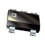
| 供应商器件封装 | SOT-23-5 |
| 共模抑制比—最小值 | 57 dB |
| 关闭 | No Shutdown |
| 其它名称 | AD8014ARTZ-REEL7-ND |
| 包装 | 带卷 (TR) |
| 压摆率 | 4600 V/µs |
| 商标 | Analog Devices |
| 增益带宽积 | - |
| 安装类型 | 表面贴装 |
| 安装风格 | SMD/SMT |
| 封装 | Reel |
| 封装/外壳 | SC-74A,SOT-753 |
| 封装/箱体 | SOT-23-5 |
| 工作温度 | -40°C ~ 85°C |
| 工作电源电压 | 4.5 V to 12 V |
| 工厂包装数量 | 3000 |
| 带宽 | 400 MHz |
| 拓扑结构 | Current Feedback |
| 放大器类型 | 电流反馈 |
| 最大功率耗散 | 500 mW |
| 最大工作温度 | + 85 C |
| 最小工作温度 | - 40 C |
| 标准包装 | 3,000 |
| 电压-电源,单/双 (±) | 4.5 V ~ 12 V, ±2.25 V ~ 6 V |
| 电压-输入失调 | 2mV |
| 电压增益dB | 123 dB |
| 电流-电源 | 1.15mA |
| 电流-输入偏置 | 5µA |
| 电流-输出/通道 | 50mA |
| 电源电压-最大 | 12 V |
| 电源电压-最小 | 4.5 V |
| 电源电流 | 1.3 mA |
| 电路数 | 1 |
| 稳定时间 | 24 ns |
| 系列 | AD8014 |
| 视频文件 | http://www.digikey.cn/classic/video.aspx?PlayerID=1364138032001&width=640&height=505&videoID=2245193153001http://www.digikey.cn/classic/video.aspx?PlayerID=1364138032001&width=640&height=505&videoID=2245193159001 |
| 转换速度 | 4000 V/us |
| 输入补偿电压 | 2 mV |
| 输出电流 | 50 mA |
| 输出类型 | - |
| 通道数量 | 1 Channel |


- 商务部:美国ITC正式对集成电路等产品启动337调查
- 曝三星4nm工艺存在良率问题 高通将骁龙8 Gen1或转产台积电
- 太阳诱电将投资9.5亿元在常州建新厂生产MLCC 预计2023年完工
- 英特尔发布欧洲新工厂建设计划 深化IDM 2.0 战略
- 台积电先进制程称霸业界 有大客户加持明年业绩稳了
- 达到5530亿美元!SIA预计今年全球半导体销售额将创下新高
- 英特尔拟将自动驾驶子公司Mobileye上市 估值或超500亿美元
- 三星加码芯片和SET,合并消费电子和移动部门,撤换高东真等 CEO
- 三星电子宣布重大人事变动 还合并消费电子和移动部门
- 海关总署:前11个月进口集成电路产品价值2.52万亿元 增长14.8%


PDF Datasheet 数据手册内容提取
a 400 MHz Low Power High Performance Amplifier AD8014 FEATURES FUNCTIONAL BLOCK DIAGRAMS Low Cost SOIC-8 (R) SOT-23-5 (RT) Low Power: 1.15 mA Max for 5 V Supply High Speed 400 MHz, –3 dB Bandwidth (G = +1) NC 1 8 NC AD8014 4000 V/ms Slew Rate VOUT 1 5 +VS 60 ns Overload Recovery –IN 2 7 +VS Fast Settling Time of 24 ns +IN 3 6 VOUT –VS 2 DVreirvye LVoiwde No oSisigenals on 50 V Lines –VS 4 AD8014 5 NC +IN 3 4 –IN 3.5 nV/(cid:214) Hz and 5 pA/(cid:214) Hz NC = NO CONNECT 5 nV/(cid:214) Hz Total Input Referred Noise @ G = +3 w/500 V Feedback Resistor Operates on +4.5 V to +12 V Supplies Low Distortion –70 dB THD @ 5 MHz Low, Temperature-Stable DC Offset Available in SOIC-8 and SOT-23-5 APPLICATIONS Photo-Diode Preamp Professional and Portable Cameras The AD8014 is a very high speed amplifier with 400 MHz, Hand Sets –3 dB bandwidth, 4000 V/m s slew rate, and 24 ns settling time. DVD/CD The AD8014 is a very stable and easy to use amplifier with fast Handheld Instruments overload recovery. The AD8014 has extremely low voltage and A-to-D Driver current noise, as well as low distortion, making it ideal for use Any Power-Sensitive High Speed System in wide-band signal processing applications. For a current feedback amplifier, the AD8014 has extremely low offset voltage and input bias specifications as well as low PRODUCT DESCRIPTION drift. The input bias current into either input is less than 15 m A The AD8014 is a revolutionary current feedback operational at +25°C with a typical drift of less than 50 nA/°C over the amplifier that attains new levels of combined bandwidth, power, industrial temperature range. The offset voltage is 5 mV max output drive and distortion. Analog Devices, Inc. uses a propri- with a typical drift less than 10 m V/°C. etary circuit architecture to enable the highest performance amplifier at the lowest power. Not only is it technically superior, For a low power amplifier, the AD8014 has very good drive but is low priced, for use in consumer electronics. This general capability with the ability to drive 2 V p-p video signals on purpose amplifier is ideal for a wide variety of applications 75 W or 50 W series terminated lines and still maintain more including battery operated equipment. than 135 MHz, 3 dB bandwidth. Rev. C Information furnished by Analog Devices is believed to be accurate and reliable. However, no responsibility is assumed by Analog Devices for its use, nor for any infringements of patents or other rights of third parties One Technology Way, P.O. Box 9106, Norwood, MA 02062-9106, U.S.A. which may result from its use. No license is granted by implication or Tel: 781/329-4700 www.analog.com otherwise under any patent or patent rights of Analog Devices. Fax: © Analog Devices, Inc.,
AD8014–SPECIFICATIONS (@ T = +258C, V = 65 V, R = 150 V, R = 1 kV, Gain = +2, unless otherwise noted) A S L F AD8014AR/RT Parameter Conditions Min Typ Max Units DYNAMIC PERFORMANCE –3 dB Bandwidth Small Signal G = +1, V = 0.2 V p-p, R = 1 kW 400 480 MHz O L G = –1, V = 0.2 V p-p, R = 1 kW 120 160 MHz O L –3 dB Bandwidth Large Signal V = 2 V p-p 140 180 MHz O V = 2 V p-p, R = 500 W 170 210 MHz O F V = 2 V p-p, R = 500 W , R = 50 W 130 MHz O F L 0.1 dB Small Signal Bandwidth V = 0.2 V p-p, R = 1 kW 12 MHz O L 0.1 dB Large Signal Bandwidth V = 2 V p-p, R = 1 kW 20 MHz O L Slew Rate, 25% to 75%, V = 4 V Step R = 1 kW , R = 500 W 4600 V/m s O L F R = 1 kW 2800 V/m s L G = –1, R = 1 kW , R = 500 W 4000 V/m s L F G = –1, R = 1 kW 2500 V/m s L Settling Time to 0.1% G = +1, V = 2 V Step, R = 1 kW 24 ns O L Rise and Fall Time 10% to 90% 2 V Step 1.6 ns G = –1, 2 V Step 2.8 ns Overload Recovery to Within 100 mV 0 V to ±4 V Step at Input 60 ns NOISE/HARMONIC PERFORMANCE Total Harmonic Distortion f = 5 MHz, V = 2 V p-p, R = 1 kW –68 dB C O L f = 5 MHz, V = 2 V p-p –51 dB C O f = 20 MHz, V = 2 V p-p –45 dB C O SFDR f = 20 MHz, V = 2 V p-p –48 dB C O Input Voltage Noise f = 10 kHz 3.5 nV/(cid:214) Hz Input Current Noise f = 10 kHz 5 pA/(cid:214) Hz Differential Gain Error NTSC, G = +2, R = 500 W 0.05 % F NTSC, G = +2, R = 500 W , R = 50 W 0.46 % F L Differential Phase Error NTSC, G = +2, R = 500 W 0.30 Degree F NTSC, G = +2, R = 500 W , R = 50 W 0.60 Degree F L Third Order Intercept f = 10 MHz 22 dBm DC PERFORMANCE Input Offset Voltage 2 5 mV T –T 2 6 mV MIN MAX Input Offset Voltage Drift 10 m V/°C Input Bias Current +Input or –Input 5 15 m A Input Bias Current Drift 50 nA/°C Input Offset Current 5 –m A Open Loop Transresistance 800 1300 kW INPUT CHARACTERISTICS Input Resistance +Input 450 kW Input Capacitance +Input 2.3 pF Input Common-Mode Voltage Range ±3.8 ±4.1 V Common-Mode Rejection Ratio V = ±2.5 V –52 –57 dB CM OUTPUT CHARACTERISTICS Output Voltage Swing R = 150 W – 3.4 ±3.8 V L R = 1 kW – 3.6 ±4.0 V L Output Current V = ±2.0 V 40 50 mA O Short Circuit Current 70 mA Capacitive Load Drive for 30% Overshoot 2 V p-p, R = 1 kW , R = 500 W 40 pF L F POWER SUPPLY Operating Range ±2.25 ±5 ±6.0 V Quiescent Current 1.15 1.3 mA Power Supply Rejection Ratio ±4 V to ±6 V –55 –58 dB Specifications subject to change without notice. –2– Rev. C
AD8014 SPECIFICATIONS (@ T = +258C, V = +5 V, R = 150 V, R = 1 kV, Gain = +2, unless otherwise noted) A S L F AD8014AR/RT Parameter Conditions Min Typ Max Units DYNAMIC PERFORMANCE –3 dB Bandwidth Small Signal G = +1, V = 0.2 V p-p, R = 1 kW 345 430 MHz O L G = –1, V = 0.2 V p-p, R = 1 kW 100 135 MHz O L –3 dB Bandwidth Large Signal V = 2 V p-p 75 100 MHz O V = 2 V p-p, R = 500 W 90 115 MHz O F V = 2 V p-p, R = 500 W , R = 75 W 100 MHz O F L 0.1 dB Small Signal Bandwidth V = 0.2 V p-p, R = 1 kW 10 MHz O L 0.1 dB Large Signal Bandwidth V = 2 V p-p 20 MHz O Slew Rate, 25% to 75%, V = 2 V Step R = 1 kW , R = 500 W 3900 V/m s O L F R = 1 kW 1100 V/m s L G = –1, R = 1 kW , R = 500 W 1800 V/m s L F G = –1, R = 1 kW 1100 V/m s L Settling Time to 0.1% G = +1, V = 2 V Step, R = 1 kW 24 ns O F Rise and Fall Time 10% to 90% 2 V Step 1.9 ns G = –1, 2 V Step 2.8 ns Overload Recovery to Within 100 mV 0 V to ±2 V Step at Input 60 ns NOISE/HARMONIC PERFORMANCE Total Harmonic Distortion f = 5 MHz, V = 2 V p-p, R = 1 kW –70 dB C O L f = 5 MHz, V = 2 V p-p –51 dB C O f = 20 MHz, V = 2 V p-p –45 dB C O SFDR f = 20 MHz, V = 2 V p-p –47 dB C O Input Voltage Noise f = 10 kHz 3.5 nV/(cid:214) Hz Input Current Noise f = 10 kHz 5 pA/(cid:214) Hz Differential Gain Error NTSC, G = +2, R = 500 W 0.06 % F NTSC, G = +2, R = 500 W , R = 50 W 0.05 % F L Differential Phase Error NTSC, G = +2, R = 500 W 0.03 Degree F NTSC, G = +2, R = 500 W , R = 50 W 0.30 Degree F L Third Order Intercept f = 10 MHz 22 dBm DC PERFORMANCE Input Offset Voltage 2 5 mV T –T 2 6 mV MIN MAX Input Offset Voltage Drift 10 m V/°C Input Bias Current +Input or –Input 5 15 m A Input Bias Current Drift 50 nA/°C Input Offset Current 5 –m A Open Loop Transresistance 750 1300 kW INPUT CHARACTERISTICS Input Resistance +Input 450 kW Input Capacitance +Input 2.3 pF Input Common-Mode Voltage Range 1.2 1.1 to 3.9 3.8 V Common-Mode Rejection Ratio V = 1.5 V to 3.5 V –52 –57 dB CM OUTPUT CHARACTERISTICS Output Voltage Swing R = 150 W to 2.5 V 1.4 1.1 to 3.9 3.6 V L R = 1 kW to 2.5 V 1.2 0.9 to 4.1 3.8 V L Output Current V = 1.5 V to 3.5 V 30 50 mA O Short Circuit Current 70 mA Capacitive Load Drive for 30% Overshoot 2 V p-p, R = 1 kW , R = 500 W 55 pF L F POWER SUPPLY Operating Range 4.5 5 12 V Quiescent Current 1.0 1.15 mA Power Supply Rejection Ratio 4 V to 5.5 V –55 –58 dB Specifications subject to change without notice. Rev. C –3–
AD8014 ABSOLUTE MAXIMUM RATINGS1 plastic. This is approximately +150°C. Even temporarily ex- Supply Voltage . . . . . . . . . . . . . . . . . . . . . . . . . . . . . . . .12.6 V ceeding this limit may cause a shift in parametric performance Internal Power Dissipation2 due to a change in the stresses exerted on the die by the pack- Small Outline Package (R) . . . . . . . . . . . . . . . . . . . . 0.75 W age. Exceeding a junction temperature of +175°C may result in SOT-23-5 Package (RT) . . . . . . . . . . . . . . . . . . . . . . 0.5 W device failure. Input Voltage Common Mode . . . . . . . . . . . . . . . . . . . . . .±V S The output stage of the AD8014 is designed for large load cur- Differential Input Voltage . . . . . . . . . . . . . . . . . . . . . . ±2.5 V rent capability. As a result, shorting the output to ground or to Output Short Circuit Duration power supply sources may result in a very large power dissipa- . . . . . . . . . . . . . . . . . . . . . .Observe Power Derating Curves tion. To ensure proper operation it is necessary to observe the Storage Temperature Range . . . . . . . . . . . . –65°C to +150°C maximum power derating tables. Operating Temperature Range . . . . . . . . . . . –40°C to +85°C Lead Temperature (Soldering 10 sec) . . . . . . . . . . . . .+300°C Table I. Maximum Power Dissipation vs. Temperature ESD (Human Body Model) . . . . . . . . . . . . . . . . . . . . +1500 V NOTES Ambient Temp Power Watts Power Watts 1Stresses above those listed under Absolute Maximum Ratings may cause perma- 8C SOT-23-5 SOIC nent damage to the device. This is a stress rating only, functional operation of the device at these or any other conditions above listed in the operational section of this –40 0.79 1.19 specification is not implied. Exposure to Absolute Maximum Ratings for any –20 0.71 1.06 extended periods may affect device reliability. 0 0.63 0.94 2Specification is for device in free air at 25°C. +20 0.54 0.81 85--LLeeaadd SSOOITC-2 P3a Pckaacgkea gqeJA q =JA 1=5 52°4C0°/CW/.W. +40 0.46 0.69 +60 0.38 0.56 MAXIMUM POWER DISSIPATION +80 0.29 0.44 The maximum power that can be safely dissipated by the AD8014 +100 0.21 0.31 is limited by the associated rise in junction temperature. The maximum safe junction temperature for plastic encapsulated devices is determined by the glass transition temperature of the CAUTION ESD (electrostatic discharge) sensitive device. Electrostatic charges as high as 4000 V readily WARNING! accumulate on the human body and test equipment and can discharge without detection. Although the AD8014 features proprietary ESD protection circuitry, permanent damage may occur on devices subjected to high energy electrostatic discharges. Therefore, proper ESD ESD SENSITIVE DEVICE precautions are recommended to avoid performance degradation or loss of functionality. –4– Rev. C
Typical Performance Characteristics–AD8014 15 2.0 G = +1 12 VO = 200mV p-p 1.0 N – dB 69 RRFL == 11kkVV VS = 65V N – dB–1.00 VO =V 0O. 2=V 0.5V AI 3 AI D G VS = +5V D G–2.0 E 0 E LIZ LIZ–3.0 VO = 1V A–3 A ORM–6 ORM–4.0 VO = 2V N–9 N–5.0 GVS = = – 615V VO = 4V –12 –6.0 RF = 1kV RL = 1kV –15 –7.0 1 10 100 1000 1 10 100 1000 FREQUENCY – MHz FREQUENCY – MHz Figure 1.Frequency Response, G = +1, VS = ±5 V and +5 V Figure 4.Bandwidth vs. Output Level—Gain of –1, Dual Supply 12 12 9 9 6 VO = 0.5V p-p VO = 1V p-p ORMALIZED GAIN – dB––3063 GRVVSOF = === + 65220V50 VpV-p RL = 50V RL = 75V ORMALIZED GAIN – dB–3603 VO = 2V p-p N–9 N–6 VS = +5V G = +2 –12 –9 RRFL == 11kkVV VO = 3V p-p –15 –12 1 10 100 1000 1 10 100 1000 FREQUENCY – MHz FREQUENCY – MHz Figure 2.Frequency Response, G = +2, V = 2 V p-p Figure 5.Bandwidth vs. Output Level—Single Supply, O G = +2 12 2 9 VO = 0.5V p-p 1 VO = 0.5V p-p 0 AIN – dB 36 VO = 1V p-p AIN – dB––21 G G ED 0 VO = 4V p-p ED –3 MALIZ–3 MALIZ–4 VO = 4V p-p VO = 2V p-p NOR–6 VS = 65V VO = 2V p-p NOR–5 VS = +5V –9 GRRFL = == + 112kkVV ––76 GRRFL = == – 111kkVV VO = 0.2V p-p –12 –8 10 100 1000 1 10 100 1000 FREQUENCY – MHz FREQUENCY – MHz Figure 3.Bandwidth vs. Output Voltage Level— Figure 6.Bandwidth vs. Output Level—Single Supply, Dual Supply, G = +2 Gain of –1 Rev. C –5–
AD8014 7.5 6.2 67..50 RF = 300V RF = 500V 66..01 VS = 65V B GAIN – d65..05 RF = 600V ESS – dB55..89 VS = +5V D N RMALIZE45..50 RF = 750V AIN FLAT55..67 NO VS = 65V RF = 1kV G5.5 G = +2 4.0 G = +2 5.4 V = 2V p-p 3.5 VROL == 125V0 pV-p 5.3 RRFL == 510500VV 3.0 5.2 1 10 100 1000 1 10 100 1000 FREQUENCY – MHz FREQUENCY – MHz Figure 7.Bandwidth vs. Feedback Resistor—Dual Supply Figure 10.Gain Flatness—Large Signal 7.5 9 6 G = +1 7.0 3 B d6.5 N – RF = 300V 0 ED GAI6.0 RF = 500V N – dB–3 G = +2 MALIZ5.5 RF = 750V GAI–6 G = +10 NOR5.0 GVS = = + +25V RF = 1kV ––192 RVSF == ±15kVV 4.5 VO = 2V p-p RL = 1kV RL = 150V –15 VO = 200mV p-p 4.0 –18 1 10 100 1000 1 10 100 1000 FREQUENCY – MHz FREQUENCY – MHz Figure 8.Bandwidth vs. Feedback Resistor—Single Supply Figure 11.Bandwidth vs. Gain—Dual Supply, R = 1 kW F 6.8 9 G = +2 6.7 RF = 1kV 6 G = +1 6.6 RL = 1kV B6.5 VO = 200mV p-p VS = 65V 3 d N – 6.4 0 MALIZED GAI666...312 VS = +5V GAIN – dB––63 RVRVSOFL ==== +112kk50VVV0mV p-p G = +2 R6.0 –9 G = +10 O N 5.9 –12 5.8 –15 5.7 5.6 –18 1 10 100 1000 1 10 100 1000 FREQUENCY – MHz FREQUENCY – MHz Figure 9.Gain Flatness—Small Signal Figure 12.Bandwidth vs. Gain—Single Supply –6– Rev. C
AD8014 0 140 0 –10 VS = 65V 120 –40 –20 G = +2 –30 RF = 1kV 100 PHASE –80 s PSRR – dB–––465000 –PSRR +PSRR VGAIN – dB8600 GAIN ––112600 HASE – Degree P 40 –200 –70 –80 20 –240 –90 0 –280 –100 1k 10k 100k 1M 10M 100M 1G 0.01 0.10 1 10 100 1000 FREQUENCY – Hz FREQUENCY – MHz Figure 13.PSRR vs. Frequency Figure 16.Transimpedance Gain and Phase vs. Frequency –20 100 –25 –30 10 V –35 – E CMRR – dB–––544050 VS = +5V VS = ±5V T RESISTANC0.11 –55 PU T –60 OU 0.01 –65 –70 –75 0.01 0.1 1 10 100 1000 0.1 1 10 100 1000 FREQUENCY – MHz FREQUENCY – MHz Figure 14.CMRR vs. Frequency Figure 17.Output Resistance vs. Frequency, VS = ±5 V and +5 V –30 3RD RL = 150V c B–50 d – 2ND RTION RL = 150V 2RNL D= 1kV O T S DI–70 ␣␣ 3RD RL = 1kV DISTORTION BELOW NOISE FLOOR –90 1 10 100 FREQUENCY – MHz Figure 15.Distortion vs. Frequency; V = ±5 V, G = +2 Figure 18.Settling Time S Rev. C –7–
AD8014 Figure 21 shows the circuit that was used to imitate a photo- diode preamp. A photodiode for this application is basically a high impedance current source that is shunted by a small ca- pacitance. In this case, a high voltage pulse from a Picosecond Pulse Labs Generator that is ac-coupled through a 20 kW resis- tor is used to simulate the high impedance current source of a photodiode. This circuit will convert the input voltage pulse into a small charge package that is converted back to a voltage by the AD8014 and the feedback resistor. In this case the feedback resistor chosen was 1.74 kW , which is a compromise between maintaining bandwidth and providing sufficient gain in the preamp stage. The circuit preserves the pulse shape very well with very fast rise time and a minimum of Figure 19.Large Signal Step Response; V = ±5 V, overshoot as shown in Figure 22. S V = 4 V Step O 1.74kV +5V 0.1mF 20kV INPUT 49.9V AD8014 49.9V O(1U03TP PURTOBE) (NO LOAD) –5V Figure 21.AD8014 as a Photodiode Preamp TEK RUN: 2.0GS/s ET AVERAGE T[ ] INPUT1 DIV Figure 20.Large Signal Step Response; V = +5 V, S V = 2 V Step O Note: On Figures 19 and 20 R = 500 W , R = 50 W and C = F S L 20 pF. OUTPUT2 500mV/DIV CH1 20.0V CH2 500mV M 25.0ns CH4 380mV APPLICATIONS CD ROM and DVD Photodiode Preamp Figure 22.Pulse Response High speed Multi-X CD ROM and DVD drives require high frequency photodiode preamps for their read channels. To mini- mize the effects of the photodiode capacitance, the low imped- ance of the inverting input of a current feedback amplifier is advantageous. Good group delay characteristics will preserve the pulse response of these pulses. The AD8014, having many ad- vantages, can make an excellent low cost, low noise, low power, and high bandwidth photodiode preamp for these applications. –8– Rev. C
AD8014 Video Drivers DRIVING CAPACITIVE LOADS The AD8014 easily drives series terminated cables with video The AD8014 was designed primarily to drive nonreactive loads. signals. Because the AD8014 has such good output drive you If driving loads with a capacitive component is desired, best can parallel two or three cables driven from the same AD8014. settling response is obtained by the addition of a small series Figure 23 shows the differential gain and phase driving one resistance as shown in Figure 26. The accompanying graph video cable. Figure 24 shows the differential gain and phase shows the optimum value for R vs. Capacitive Load. It is SERIES driving two video cables. Figure 25 shows the differential gain worth noting that the frequency response of the circuit when and phase driving three video cables. driving large capacitive loads will be dominated by the passive roll-off of R and C . SERIES L % N – 0.10 0.00 0.02 0.04 0.05 0.05 0.05 0.04 0.04 0.04 0.04 0.03 40 AI G 0.05 L A TI 0.00 N RE–0.05 E FF–0.10 30 DI V DIFFERENTIALHASE – Degrees––000000......642024000000 0.00 0.01 0.10 0.21 0.26 0.28 0.29 0.30 0.30 0.30 0.30 R – SERIES20 P–0.60 1ST 2ND 3RD 4TH 5TH 6TH 7TH 8TH 9TH 10TH 11TH Figure 23.Differential Gain and Phase R = 500, ±5 V, R = F L 150 W , Driving One Cable, G = +2 10 0 5 10 15 20 25 CL – pF Figure 26.Driving Capacitive Load % N – 0.30 0.00 –0.02 0.03 0.05 0.06 0.06 0.05 0.05 0.07 0.10 0.14 Choosing Feedback Resistors AI 0.20 L G 0.10 Changing the feedback resistor can change the performance of TIA 0.00 the AD8014 like any current feedback op amp. The table below N–0.10 E illustrates common values of the feedback resistor and the per- ER–0.20 FF–0.30 formance which results. DI 0.00 0.07 0.24 0.40 0.43 0.44 0.43 0.40 0.35 0.26 0.16 s 0.60 DIFFERENTIALPHASE – Degree–––000000......246420000000 Gain R R Table –VRI3IO. d ==B 16 Bk0VW.2 V R–V3O d ==B 16 5B00W .V2 V F G L L 1ST 2ND 3RD 4TH 5TH 6TH 7TH 8TH 9TH 10TH 11TH +1 1 kW Open 480 430 Figure 24.Differential Gain and Phase R = 500, ±5 V, R = 75 W , Driving Two Cables, G = +2 F L +2 1 kW 1 kW 280 260 +10 1 kW 111 W 50 45 –1 1 kW 1 kW 160 150 % –2 1 kW 499 W 140 130 N – 0.80 0.00 0.44 0.52 0.54 0.52 0.52 0.50 0.48 0.47 0.44 0.45 –10 1 kW 100 W 45 40 AI 0.60 G 0.40 +2 2 kW 2 kW 200* 180* L 0.20 TIA 0.00 +2 750 W 750 W 260* 210* REN––00..4200 +2 499 W 499 W 280* 230* E–0.60 DIFF–0.80 *VO = ±1 V. 0.00 0.10 0.32 0.53 0.57 0.59 0.58 0.56 0.54 0.51 0.48 s 0.80 RENTIAL– Degree 0000....64200000 DIFFEHASE –––000...246000 P–0.80 1ST 2ND 3RD 4TH 5TH 6TH 7TH 8TH 9TH 10TH 11TH Figure 25.Differential Gain and Phase R = 500, ±5 V, R = F L 50 W , Driving Three Cables, G = +2 Rev. C –9–
AD8014 OUTLINE DIMENSIONS 5.00(0.1968) 4.80(0.1890) 8 5 4.00(0.1574) 6.20(0.2441) 3.80(0.1497) 1 4 5.80(0.2284) 1.27(0.0500) 0.50(0.0196) BSC 1.75(0.0688) 0.25(0.0099) 45° 0.25(0.0098) 1.35(0.0532) 8° 0.10(0.0040) 0° COPLANARITY 0.51(0.0201) 0.10 SEATING 0.31(0.0122) 0.25(0.0098) 10..2470((00..00510507)) PLANE 0.17(0.0067) COMPLIANTTOJEDECSTANDARDSMS-012-AA C(RINOEFNPEATRRREOENNLCLTEIHNEOGSNDELISYM)AEANNRDSEIOARRNOESUNANORDETEDAIN-POMPFRIFLOLMPIMIRLELIATIMTEEERTFSEO;RIRNECUQHSUEDIVIINMAELDENENSSTIIOGSNNFS.OR 012407-A Figure 27. 8-Lead Standard Small Outline Package [SOIC_N] Narrow Body (R-8) Dimensions shown in millimeters and (inches) 3.00 2.90 2.80 1.70 5 4 3.00 1.60 2.80 1.50 2.60 1 2 3 0.95 BSC 1.90 BSC 1.30 1.15 0.90 1.45 MAX 0.20 MAX 0.95 MIN 0.08 MIN 0.55 0.15 MAX 10° 0.45 0.05 MIN 0.50 MAX SPELAATNIENG 5° B0S.2C0 0.35 0.35 MIN 0° COMPLIANT TO JEDEC STANDARDS MO-178-AA 121608-A Figure 28. 5-Lead Small Outline Transistor Package [SOT-23] (RJ-5) Dimensions shown in millimeters ORDERING GUIDE Model1 Temperature Range Package Description Package Option Branding AD8014AR −40°C to +85°C 8-Lead SOIC_N R-8 AD8014AR -REEL7 −40°C to +85°C 8-Lead SOIC_N R-8 AD8014ARZ −40°C to +85°C 8-Lead SOIC_N R-8 AD8014ARZ-REEL −40°C to +85°C 8-Lead SOIC_N R-8 AD8014ARZ-REEL7 −40°C to +85°C 8-Lead SOIC_N R-8 AD8014ART-R2 −40°C to +85°C 5-Lead SOT-23 RJ-5 HAA AD8014ART-REEL7 −40°C to +85°C 5-Lead SOT-23 RJ-5 HAA AD8014ARTZ-R2 −40°C to +85°C 5-Lead SOT-23 RJ-5 H09 AD8014ARTZ-REEL −40°C to +85°C 5-Lead SOT-23 RJ-5 H09 AD8014ARTZ-REEL7 −40°C to +85°C 5-Lead SOT-23 RJ-5 H09 1 Z = RoHS Compliant Part. -10- Rev. C
AD8014 REVISION HISTORY Changes to Figure 22 ........................................................................ 8 Updated Outline Dimensions ........................................................ 10 Changes to Ordering Guide ........................................................... 10 ©1998–2010 Analog Devices, Inc. All rights reserved. Trademarks and registered trademarks are the property of their respective owners. D08930-0-4/10(C) Rev. C -11-
Mouser Electronics Authorized Distributor Click to View Pricing, Inventory, Delivery & Lifecycle Information: A nalog Devices Inc.: AD8014ARTZ-REEL7 AD8014ARZ AD8014ARZ-REEL AD8014ARZ-REEL7 AD8014ARTZ-R2