ICGOO在线商城 > 集成电路(IC) > 线性 - 放大器 - 仪表,运算放大器,缓冲器放大器 > LMV722IDR

 Datasheet下载
- 型号: LMV722IDR
- 制造商: Texas Instruments
- 库位|库存: xxxx|xxxx
- 要求:
| 数量阶梯 | 香港交货 | 国内含税 |
| +xxxx | $xxxx | ¥xxxx |
查看当月历史价格
查看今年历史价格
LMV722IDR产品简介:
ICGOO电子元器件商城为您提供LMV722IDR由Texas Instruments设计生产,在icgoo商城现货销售,并且可以通过原厂、代理商等渠道进行代购。 LMV722IDR价格参考¥2.87-¥7.08。Texas InstrumentsLMV722IDR封装/规格:线性 - 放大器 - 仪表,运算放大器,缓冲器放大器, 通用 放大器 2 电路 满摆幅 8-SOIC。您可以下载LMV722IDR参考资料、Datasheet数据手册功能说明书,资料中有LMV722IDR 详细功能的应用电路图电压和使用方法及教程。
LMV722IDR 是 Texas Instruments(德州仪器)推出的一款低功耗、轨到轨输入/输出的运算放大器,属于线性 - 放大器 - 仪表、运算放大器、缓冲器放大器分类。它具有小型化封装(如 SOT-23)、低电源电流和宽电源电压范围等特点,适合多种应用场景。以下是其主要应用领域:

1. 便携式电子设备
   LMV722IDR 的低功耗特性使其非常适合电池供电的便携式设备,例如智能手机、平板电脑、可穿戴设备(如智能手表和健康监测器)等。这些设备需要在有限的电池容量下运行,而 LMV722IDR 的低静态电流可以延长设备的续航时间。

2. 传感器信号调理
   在工业自动化、医疗设备和消费电子中,传感器信号通常需要被放大和处理。LMV722IDR 的轨到轨输入/输出能力使其能够精确地放大来自传感器的小信号,适用于压力传感器、温度传感器、加速度计等信号调理电路。

3. 音频信号处理
   由于其低失真和低噪声性能,LMV722IDR 可用于音频信号的放大和处理,例如麦克风前置放大器、耳机驱动器或便携式音频设备中的音量控制电路。

4. 电源监控与管理
   在电源管理系统中,LMV722IDR 可用于电压监测、电流检测和电池电量监控。其宽电源电压范围(1.8V 至 5.5V)使得它能够在各种电源条件下稳定工作。

5. 医疗设备
   在医疗领域,LMV722IDR 可用于心电图(ECG)、脉搏血氧仪和其他便携式医疗设备中的信号放大和处理。其低功耗和小尺寸特点非常适合对体积和能耗要求严格的医疗设备。

6. 通信与物联网(IoT)设备
   在物联网设备中,LMV722IDR 可用于信号放大、滤波和数据采集。例如,在无线传感器网络中,它可以放大传感器输出信号以便于后续处理和传输。

总之,LMV722IDR 凭借其低功耗、小尺寸和高性能的特点,广泛应用于便携式设备、传感器信号处理、音频系统、电源管理和医疗设备等领域,是一款多功能且高效的运算放大器。
| 参数 | 数值 |
| -3db带宽 | - |
| 产品目录 | 集成电路 (IC)半导体 |
| 描述 | IC OPAMP GP R-R 10MHZ DUAL 8SOIC运算放大器 - 运放 10-MHz L-N L-V L-P |
| 产品分类 | Linear - Amplifiers - Instrumentation, OP Amps, Buffer Amps集成电路 - IC |
| 品牌 | Texas Instruments |
| 产品手册 | http://www.ti.com/litv/slos470c |
| 产品图片 |
|
| rohs | 符合RoHS无铅 / 符合限制有害物质指令(RoHS)规范要求 |
| 产品系列 | 放大器 IC,运算放大器 - 运放,Texas Instruments LMV722IDR- |
| 数据手册 | |
| 产品型号 | LMV722IDR |
| 产品种类 | 运算放大器 - 运放 |
| 供应商器件封装 | 8-SOIC |
| 共模抑制比—最小值 | 70 dB |
| 关闭 | No Shutdown |
| 其它名称 | 296-36935-1 |
| 包装 | 剪切带 (CT) |
| 单位重量 | 72.600 mg |
| 单电源电压 | 2.2 V to 5 V |
| 压摆率 | 5.25 V/µs |
| 商标 | Texas Instruments |
| 增益带宽生成 | 10 MHz |
| 增益带宽积 | 10MHz |
| 安装类型 | 表面贴装 |
| 安装风格 | SMD/SMT |
| 封装 | Reel |
| 封装/外壳 | 8-SOIC(0.154",3.90mm 宽) |
| 封装/箱体 | SOIC-8 |
| 工作温度 | -40°C ~ 105°C |
| 工作电源电压 | 2.2 V to 5 V |
| 工厂包装数量 | 2500 |
| 放大器类型 | 通用 |
| 最大工作温度 | + 85 C |
| 最小工作温度 | - 40 C |
| 标准包装 | 1 |
| 电压-电源,单/双 (±) | 2.2 V ~ 5 V |
| 电压-输入失调 | 80µV |
| 电流-电源 | 2.01mA |
| 电流-输入偏置 | 260nA |
| 电流-输出/通道 | 52.6mA |
| 电源电流 | 2.4 mA |
| 电路数 | 2 |
| 系列 | LMV722 |
| 设计资源 | http://www.digikey.com/product-highlights/cn/zh/texas-instruments-webench-design-center/3176 |
| 转换速度 | 4.9 V/us |
| 输入偏压电流—最大 | 260 nA (typ) |
| 输入参考电压噪声 | 8.5 nV |
| 输入补偿电压 | 3 mV |
| 输出电流 | 17.6 mA |
| 输出类型 | 满摆幅 |
| 通道数量 | 2 Channel |


- 商务部:美国ITC正式对集成电路等产品启动337调查
- 曝三星4nm工艺存在良率问题 高通将骁龙8 Gen1或转产台积电
- 太阳诱电将投资9.5亿元在常州建新厂生产MLCC 预计2023年完工
- 英特尔发布欧洲新工厂建设计划 深化IDM 2.0 战略
- 台积电先进制程称霸业界 有大客户加持明年业绩稳了
- 达到5530亿美元!SIA预计今年全球半导体销售额将创下新高
- 英特尔拟将自动驾驶子公司Mobileye上市 估值或超500亿美元
- 三星加码芯片和SET,合并消费电子和移动部门,撤换高东真等 CEO
- 三星电子宣布重大人事变动 还合并消费电子和移动部门
- 海关总署:前11个月进口集成电路产品价值2.52万亿元 增长14.8%


PDF Datasheet 数据手册内容提取
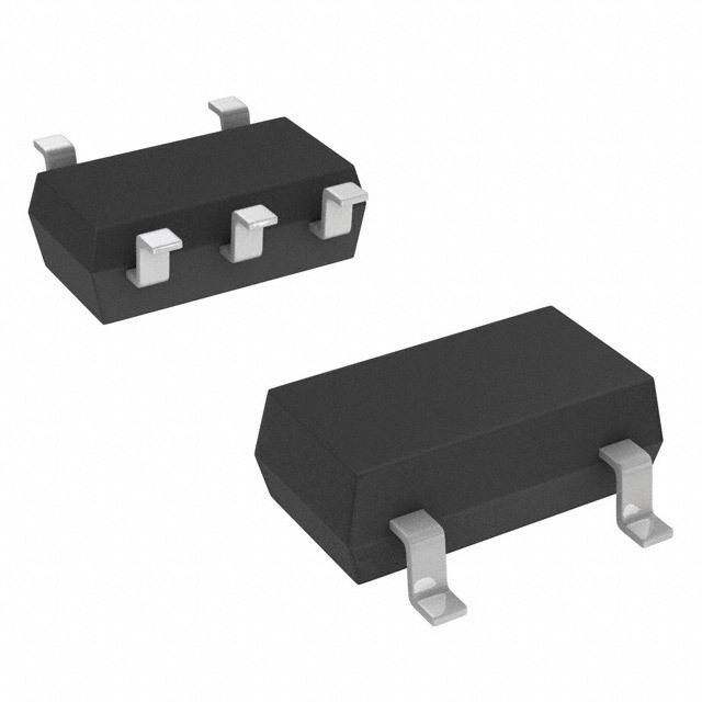
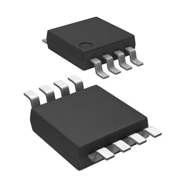
LMV721 LMV722 www.ti.com SLOS470C–JUNE2005–REVISEDSEPTEMBER2010 10-MHz LOW-NOISE LOW-VOLTAGE LOW-POWER OPERATIONAL AMPLIFIERS CheckforSamples:LMV721,LMV722 FEATURES 1 LMV721(cid:1)DBV or DCK PACKAGE • Power-SupplyVoltageRange:2.2Vto5.5V (TOP VIEW) • LowSupplyCurrent:930mA/Amplifierat2.2V • HighUnity-GainBandwidth:10MHz OUT 1 5 VCC+ • Rail-to-RailOutputSwing VCC− 2 IN+ 3 4 IN− – 600-Ω Load:120mVFromEitherRailat 2.2V – 2-kΩLoad:50mVFromEitherRailat2.2V LMV722(cid:1)D, DGK, OR DRG PACKAGE • InputCommon-ModeVoltageRangeIncludes (TOP VIEW) Ground • InputVoltageNoise:9nV/√Hzatf=1kHz 1OUT 1 8 VCC+ 1IN− 2 7 2OUT APPLICATIONS 1IN+ 3 6 2IN− • CellularandCordlessPhones VCC− 4 5 2IN+ • ActiveFilterandBuffers • LaptopsandPDAs • BatteryPoweredElectronics DESCRIPTION/ORDERING INFORMATION The LMV721 (single) and LMV722 (dual) are low-noise low-voltage low-power operational amplifiers that can be designed into a wide range of applications. The LMV721 and LMV722 have a unity-gain bandwidth of 10 MHz, a slewrateof5V/ms,andaquiescentcurrentof930 mA/amplifierat2.2V. The LMV721 and LMV722 are designed to provide optimal performance in low-voltage and low-noise systems. They provide rail-to-rail output swing into heavy loads. The input common-mode voltage range includes ground, and the maximum input offset voltage are 3.5 mV (over recommended temperature range) for the devices. Their capacitiveloadcapabilityisalsogoodatlowsupplyvoltages.Theoperatingrangeisfrom2.2Vto5.5V. ORDERINGINFORMATION(1) T PACKAGE(2) ORDERABLEPARTNUMBER TOP-SIDEMARKING(3) A Reelof3000 LMV721IDCKR SC-70–DCK RK_ Single Reelof250 LMV721IDCKT SOT-23–DBV Reelof3000 LMV721IDBVR RBF_ –40°Cto105°C Reelof2500 LMV722IDR SOIC–D MV722I Tubeof75 LMV722ID Dual VSSOP–DGK Reelof2500 LMV722IDGKR R6_ QFN–DRG Reelof2500 LMV722IDRGR ZYY (1) Forthemostcurrentpackageandorderinginformation,seethePackageOptionAddendumattheendofthisdocument,orseetheTI websiteatwww.ti.com. (2) Packagedrawings,thermaldata,andsymbolizationareavailableatwww.ti.com/packaging. (3) DBV/DCK/DGK:Theactualtop-sidemarkinghasoneadditionalcharacterthatdesignatesthewaferfab/assemblysite. 1 Pleasebeawarethatanimportantnoticeconcerningavailability,standardwarranty,anduseincriticalapplicationsofTexas Instrumentssemiconductorproductsanddisclaimerstheretoappearsattheendofthisdatasheet. PRODUCTIONDATAinformationiscurrentasofpublicationdate. Copyright©2005–2010,TexasInstrumentsIncorporated Products conform to specifications per the terms of the Texas Instruments standard warranty. Production processing does not necessarilyincludetestingofallparameters.
LMV721 LMV722 SLOS470C–JUNE2005–REVISEDSEPTEMBER2010 www.ti.com Typical Application R5 VCC C1 Electret R3 Microphone R4 Input VCC R1 − Output + C2 R2 Absolute Maximum Ratings(1) overoperatingfree-airtemperaturerange(unlessotherwisenoted) MIN MAX UNIT V –V Supplyvoltage(2) 6 V CC+ CC– V Differentialinputvoltage(3) ±Supplyvoltage V ID Dpackage(5) 97 DBVpackage(5) 206 q Packagethermalimpedance(4) DCKpackage(5) 252 °C/W JA DGKpackage(5) 172 DRGpackage(6) 50.7 T Operatingvirtual-junctiontemperature 150 °C J T Storagetemperaturerange –65 150 °C stg (1) Stressesbeyondthoselistedunderabsolutemaximumratingsmaycausepermanentdamagetothedevice.Thesearestressratings only,andfunctionaloperationofthedeviceattheseoranyotherconditionsbeyondthoseindicatedunderrecommendedoperating conditionsisnotimplied.Exposuretoabsolute-maximum-ratedconditionsforextendedperiodsmayaffectdevicereliability. (2) Allvoltagevalues(exceptdifferentialvoltagesandV specifiedforthemeasurementofI )arewithrespecttothenetworkGND. CC OS (3) DifferentialvoltagesareatIN+withrespecttoIN−. (4) MaximumpowerdissipationisafunctionofT(max),q ,andT .Themaximumallowablepowerdissipationatanyallowableambient J JA A temperatureisP =(T(max)–T )/q .OperatingattheabsolutemaximumT of150°Ccanaffectreliability. D J A JA J (5) ThepackagethermalimpedanceiscalculatedinaccordancewithJESD51-7. (6) ThepackagethermalimpedanceiscalculatedinaccordancewithJESD51-5. Recommended Operating Conditions MIN MAX UNIT V –V Supplyvoltage 2.2 5.5 V CC+ CC– T Operatingvirtual-junctiontemperature –40 105 °C J ESD Protection TYP UNIT Human-BodyModel 2000 V MachineModel 100 V 2 SubmitDocumentationFeedback Copyright©2005–2010,TexasInstrumentsIncorporated ProductFolderLink(s):LMV721LMV722
LMV721 LMV722 www.ti.com SLOS470C–JUNE2005–REVISEDSEPTEMBER2010 Electrical Characteristics V =2.2V,V =GND,V =V /2,V =V /2,andR >1MΩ(unlessotherwisenoted) CC+ CC− ICR CC+ O CC+ L PARAMETER TESTCONDITIONS T MIN TYP MAX UNIT J 25°C 0.02 3 V Inputoffsetvoltage mV IO –40°Cto105°C 3.5 TCV Inputoffsetvoltageaveragedrift 25°C 0.6 mV/°C IO I Inputbiascurrent 25°C 260 nA IB I Inputoffsetcurrent 25°C 25 nA IO 25°C 70 88 CMMR Common-moderejectionratio V =0Vto1.3V dB ICR –40°Cto105°C 64 V =2.2Vto5V, 25°C 80 90 PSRR Power-supplyrejectionratio CC+ dB VO=0,VICR=0 –40°Cto105°C 70 CMRR≥50dB –0.3 V Inputcommon-modevoltage 25°C V ICR 1.3 R =600Ω, 25°C 75 81 L VO=0.75Vto2V –40°Cto105°C 70 A Large-signalvoltagegain dB VD R =2kΩ, 25°C 75 84 L VO=0.5Vto2.1V –40°Cto105°C 70 25°C 2.090 2.125 R =600ΩtoV /2 L CC+ –40°Cto105°C 2.065 25°C 0.071 0.120 –40°Cto105°C 0.145 V Outputswing V O 25°C 2.150 2.177 R =2kΩtoV /2 L CC+ –40°Cto105°C 2.125 25°C 0.056 0.080 –40°Cto105°C 0.105 Sourcing,V =0V, 25°C 10 14.9 O VIN(diff)=±0.5V –40°Cto105°C 5 I Outputcurrent mA O Sinking,V =2.2V, 25°C 10 17.6 O VIN(diff)=±0.5V –40°Cto105°C 5 25°C 0.93 1.3 LMV721 –40°Cto105°C 1.5 I Supplycurrent mA CC 25°C 1.81 2.4 LMV722 –40°Cto105°C 2.6 SR Slewrate(1) 25°C 4.9 V/ms GBW Gainbandwidthproduct 25°C 10 MHz Φ Phasemargin 25°C 67.4 ° m G Gainmargin 25°C –9.8 dB m V Input-referredvoltagenoise f=1kHz 25°C 9 nV/√Hz n I Input-referredcurrentnoise f=1kHz 25°C 0.3 pA/√Hz n f=1kHz,AV=1, THD Totalharmonicdistortion 25°C 0.004 % R =600Ω,V =500mV L O pp (1) Connectedasvoltagefollowerwith1-Vstepinput.Numberspecifiedistheslowerofthepositiveandnegativeslewrate. Copyright©2005–2010,TexasInstrumentsIncorporated SubmitDocumentationFeedback 3 ProductFolderLink(s):LMV721LMV722
LMV721 LMV722 SLOS470C–JUNE2005–REVISEDSEPTEMBER2010 www.ti.com Electrical Characteristics V =5V,V =GND,V =V /2,V =V /2,andR >1MΩ(unlessotherwisenoted) CC+ CC− ICR CC+ O CC+ L PARAMETER TESTCONDITIONS T MIN TYP MAX UNIT J 25°C –0.08 3 V Inputoffsetvoltage mV IO –40°Cto105°C 3.5 TCV Inputoffsetvoltageaveragedrift 25°C 0.6 mV/°C IO I Inputbiascurrent 25°C 260 nA IB I Inputoffsetcurrent 25°C 25 nA IO 25°C 80 89 CMMR Common-moderejectionratio V =0Vto4.1V dB ICR –40°Cto105°C 75 V =2.2Vto5V, 25°C 70 90 PSRR Power-supplyrejectionratio CC+ dB VO=0,VICR=0 –40°Cto105°C 64 CMRR≥50dB –0.3 V Inputcommon-modevoltage 25°C V ICR 4.1 R =600Ω, 25°C 80 87 L VO=0.75Vto4.8V –40°Cto105°C 70 A Large-signalvoltagegain dB VD R =2kΩ, 25°C 80 94 L VO=0.7Vto4.9V –40°Cto105°C 70 25°C 4.84 4.882 R =600ΩtoV /2 L CC+ –40°Cto105°C 4.815 25°C 0.134 0.19 –40°Cto105°C 0.215 V Outputswing V O 25°C 4.93 4.952 R =2kΩtoV /2 L CC+ –40°Cto105°C 4.905 25°C 0.076 0.11 –40°Cto105°C 0.135 Sourcing,V =0V, 25°C 20 52.6 O VIN(diff)=±0.5V –40°Cto105°C 12 I Outputcurrent mA O Sinking,V =2.2V, 25°C 15 23.7 O VIN(diff)=±0.5V –40°Cto105°C 8.5 25°C 1.03 1.4 LMV721 –40°Cto105°C 1.7 I Supplycurrent mA CC 25°C 2.01 2.4 LMV722 –40°Cto105°C 2.8 SR Slewrate(1) 25°C 5.25 V/ms GBW Gainbandwidthproduct 25°C 10 MHz Φ Phasemargin 25°C 72 ° m G Gainmargin 25°C –11 dB m V Input-referredvoltagenoise f=1kHz 25°C 8.5 nV/√Hz n I Input-referredcurrentnoise f=1kHz 25°C 0.2 pA/√Hz n f=1kHz,AV=1, THD Totalharmonicdistortion 25°C 0.001 % R =600Ω,V =500mV L O pp (1) Connectedasvoltagefollowerwith1-Vstepinput.Numberspecifiedistheslowerofthepositiveandnegativeslewrate. 4 SubmitDocumentationFeedback Copyright©2005–2010,TexasInstrumentsIncorporated ProductFolderLink(s):LMV721LMV722
LMV721 LMV722 www.ti.com SLOS470C–JUNE2005–REVISEDSEPTEMBER2010 TYPICAL CHARACTERISTICS SUPPLYCURRENT SOURCINGCURRENT vs vs SUPPLYVOLTAGE OUTPUTVOLTAGE 1.4 100 V =2.2V CC 1.3 TA=125°C TA=85°C 1.2 A m A –m 1.1 ent– 10 rrent 1 Curr Cu 0.9 ng y ci ppl 0.8 TA=25°C our Su 0.7 TA=–40°C –S 1 I–CC 0.6 Isource 0.5 0.1 0.4 0.001 0.01 0.1 1 10 2 2.5 3 3.5 4 4.5 5 5.5 6 OutputVoltageReferencedtoV –V V –SupplyVoltage–V CC CC SOURCINGCURRENT SINKINGCURRENT vs vs OUTPUTVOLTAGE OUTPUTVOLTAGE 100 100 VCC=5V VCC=2.2V A m A m – ent 10 nt– 10 Curr urre g C n g ci n ur ki o n S 1 Si 1 – – Isource Isink 0.1 0.1 0.001 0.01 0.1 1 10 0.001 0.01 0.1 1 10 OutputVoltageReferencedtoV –V OutputVoltageReferencedtoV –V CC CC Copyright©2005–2010,TexasInstrumentsIncorporated SubmitDocumentationFeedback 5 ProductFolderLink(s):LMV721LMV722
LMV721 LMV722 SLOS470C–JUNE2005–REVISEDSEPTEMBER2010 www.ti.com TYPICAL CHARACTERISTICS (continued) SINKINGCURRENT OUTPUTVOLTAGESWING vs vs OUTPUTVOLTAGE SUPPLYVOLTAGE 100 0.3 V =5V CC 0.2 V A m m – nt– 10 age 0.1 urre Volt C et 0 g s kin Off Sin 1 ut -0.1 p – n Isink V–IIO -0.2 0.1 -0.3 0.001 0.01 0.1 1 10 2 2.5 3 3.5 4 4.5 5 OutputVoltageReferencedtoV –V V –SupplyVoltage–V CC CC INPUTOFFSETVOLTAGE INPUTOFFSETVOLTAGE vs vs INPUTCOMMON-MODEVOLTAGE INPUTCOMMON-MODEVOLTAGE 0.3 0.3 V =2.2V V =5V CC CC 0.2 0.2 V V m m – – ge 0.1 ge 0.1 a a olt olt V V et 0 et 0 s s Off Off ut -0.1 ut -0.1 p p n n I I – – VIO -0.2 VIO -0.2 -0.3 -0.3 0 0.3 0.6 0.9 1.2 1.5 0 0.5 1 1.5 2 2.5 3 3.5 4 V –InputCommon-ModeVoltage–V V –InputCommon-ModeVoltage–V ICR ICR 6 SubmitDocumentationFeedback Copyright©2005–2010,TexasInstrumentsIncorporated ProductFolderLink(s):LMV721LMV722
LMV721 LMV722 www.ti.com SLOS470C–JUNE2005–REVISEDSEPTEMBER2010 TYPICAL CHARACTERISTICS (continued) INPUTVOLTAGE INPUTVOLTAGE vs vs OUTPUTVOLTAGE OUTPUTVOLTAGE 0.3 0.3 V =2.2V V =5V CC CC 0.2 0.2 mV mV – – ge 0.1 ge 0.1 a a olt olt V V al 0 al 0 nti nti e e er er Diff -0.1 Diff -0.1 ut ut p p In -0.2 In -0.2 -0.3 -0.3 0 0.5 1 1.5 2 2.5 0 0.5 1 1.5 2 2.5 3 3.5 4 4.5 5 OutputVoltage–V OutputVoltage–V INPUTVOLTAGENOISE INPUTCURRENTNOISE vs vs FREQUENCY FREQUENCY 100 100 √HzHz √HzHz µV/ pA/ 10 – – e e s s oi oi N 10 N ge nt Volta Curre 1 ut ut p p n n I I 1 0.1 1.E1+001 1.1E0+002 1.E1+k03 1.1E0+k04 11.E0+00k5 1.E1+001 1.1E0+002 1.E1+k03 1.E1+00k4 f–Frequency–Hz f–Frequency–Hz Copyright©2005–2010,TexasInstrumentsIncorporated SubmitDocumentationFeedback 7 ProductFolderLink(s):LMV721LMV722
LMV721 LMV722 SLOS470C–JUNE2005–REVISEDSEPTEMBER2010 www.ti.com TYPICAL CHARACTERISTICS (continued) PSRR PSRR vs vs FREQUENCY FREQUENCY 120 120 V =2.2V V =5V CC CC 100 100 80 80 B B d d – – R 60 R 60 R R S S P P 40 40 20 20 0 0 1.1E0+002 1.E1+k03 1.1E0+k04 11.E0+00k5 1.E1+M06 1.1E0+M07 1.1E0+002 1.E1+k03 1.1E0+k04 11.E0+00k5 1.E1+M06 1.1E0+M07 f–Frequency–Hz f–Frequency–Hz GAINANDPHASE GAINANDPHASE vs vs FREQUENCY FREQUENCY 80 130 80 130 V =2.2V V =5V CC CC 70 115 70 115 Phase Phase 60 100 60 100 Gain 50 85 50 Gain 85 40 70 g 40 70 g B e B e d d d d – 30 55 – – 30 55 – ain ase ain ase G 20 40 h G 20 40 h P P 10 25 10 25 0 10 0 10 -10 -5 -10 -5 -20 -20 -20 -20 1.E1+k03 1.1E0+k04 11.E0+00k5 1.E1+M06 1.1E0+M07 11.E00+M08 1.E1+k03 1.1E0+k04 11.E0+00k5 1.E1M+06 1.1E0+M07 11.0E0+M08 f–Frequency–Hz f–Frequency–Hz 8 SubmitDocumentationFeedback Copyright©2005–2010,TexasInstrumentsIncorporated ProductFolderLink(s):LMV721LMV722
LMV721 LMV722 www.ti.com SLOS470C–JUNE2005–REVISEDSEPTEMBER2010 TYPICAL CHARACTERISTICS (continued) SLEWRATE THD vs vs SUPPLYVOLTAGE FREQUENCY 6 1 V =2.2V CC 5.8 5.6 0.1 s 5.4 µ V/ – 5.2 % e at – 0.01 R 5 D w Rising TH Sle 4.8 – R 4.6 S 0.001 4.4 Falling 4.2 0.0001 4 110000 1010k0 11000k00 1010000k00 2 2.5 3 3.5 4 4.5 5 f–Frequency–Hz V –SupplyVoltage–V CC PULSERESPONSE PULSERESPONSE V =R 5=V,2Rk©= ,2C kΩ=,2C1.=2 2n1F.,2R nF=,R0©= 0Ω V R= 5=V2,kR©=, C2 k=Ω2,1C.2=n 2F1,.R2 n=F,2R.1©= 2.1Ω CC L L L L O O CC L L L L O O n n o o si si vi vi Di Di r r e e p p V V 5 5 2 2 0. 0. 2µsperDivision 2µsperDivision Copyright©2005–2010,TexasInstrumentsIncorporated SubmitDocumentationFeedback 9 ProductFolderLink(s):LMV721LMV722
LMV721 LMV722 SLOS470C–JUNE2005–REVISEDSEPTEMBER2010 www.ti.com TYPICAL CHARACTERISTICS (continued) PULSERESPONSE PULSERESPONSE V R= 5=V2,kR©=, C2 k=Ω2,1C.2=n 2F1,.R2 n=F,9R.5©= 9.5Ω V R= 5=V1,0Rk©= ,1C0 k=Ω2,1C.2=n 2F1,.R2 n=F,0R©= 0Ω CC L L L L O O CC L L L L O O n n o o si si vi vi Di Di r r e e p p V V 5 5 2 2 0. 0. 2µsperDivision 2µsperDivision PULSERESPONSE PULSERESPONSE V R= 5=V6,0R0©=, 6C00=Ω2,1C.2=n F2,1R.2 n=F0,R©= 0Ω V = R2.2=V2,R©,=C 2=Ω2,C.12=n 2F.,1R2 n=F,0R©= 0Ω CC L L L L O O CC L L L L O O Division Division per per V V m 5 2 0 0. 25 2µsperDivision 1µsperDivision PULSERESPONSE PULSERESPONSE VCC= 2R.L2=V,2RkL©= ,2C kLΩ=,2C.L1=2 2n.F1,2R nOF=,R0O©= 0Ω VCC= R2L.2=V1,0RkL=© ,1C0 Lk=Ω,2C.1L2=n 2F.1,2R On=F,0R©O= 0Ω n n o o si si vi vi Di Di r r e e p p V V m m 0 0 5 5 2 2 1µsperDivision 1µsperDivision 10 SubmitDocumentationFeedback Copyright©2005–2010,TexasInstrumentsIncorporated ProductFolderLink(s):LMV721LMV722
LMV721 LMV722 www.ti.com SLOS470C–JUNE2005–REVISEDSEPTEMBER2010 TYPICAL CHARACTERISTICS (continued) PULSERESPONSE PULSERESPONSE V = 2R.2V=,1R0=k ©10, CkΩ=,C2.1=2 2n.1F2, RnF,=R2.2= ©2.2Ω V = R2.2=V1,0Rk=© 1,0C kΩ=,2C.12= n2F.1,2R nF=,1R1.5= ©11.5Ω CC L L L L O O CC L L L L O O n n o o si si vi vi Di Di r r e e p p V V m m 0 0 5 5 2 2 1µsperDivision 1µsperDivision PULSERESPONSE V = R2.2=V6,0R0©= ,6C00=Ω1,C.89=n 1F.,8R9 n=F,0R©= 0Ω CC L L L L O O n o si vi Di r e p V m 0 5 2 1µsperDivision Copyright©2005–2010,TexasInstrumentsIncorporated SubmitDocumentationFeedback 11 ProductFolderLink(s):LMV721LMV722
LMV721 LMV722 SLOS470C–JUNE2005–REVISEDSEPTEMBER2010 www.ti.com REVISION HISTORY ChangesfromRevisionB(August2010)toRevisionC Page • Changedalltemperatureparametersfrommaxof85°Cto105°C ...................................................................................... 1 • Changedsupplyvoltagemaxvalueto6inAbsoluteMaximumRatingstable ..................................................................... 2 • ChangedsupplyvoltageMAXvalueto5.5inRecommendedOperatingConditionstable ................................................. 2 • ChangedA ,V testconditonsforR =600Ω:0.75Vto4.8V ........................................................................................ 4 VD O L • ChangedA ,V testconditonsforR =2kΩΩ:0.75Vto4.8V ....................................................................................... 4 VD O L 12 SubmitDocumentationFeedback Copyright©2005–2010,TexasInstrumentsIncorporated ProductFolderLink(s):LMV721LMV722
PACKAGE OPTION ADDENDUM www.ti.com 6-Feb-2020 PACKAGING INFORMATION Orderable Device Status Package Type Package Pins Package Eco Plan Lead/Ball Finish MSL Peak Temp Op Temp (°C) Device Marking Samples (1) Drawing Qty (2) (6) (3) (4/5) LMV721IDBVR ACTIVE SOT-23 DBV 5 3000 Green (RoHS NIPDAU Level-1-260C-UNLIM -40 to 105 (RBFA, RBFM) & no Sb/Br) LMV721IDCKR ACTIVE SC70 DCK 5 3000 Green (RoHS NIPDAU | NIPDAUAG Level-1-260C-UNLIM -40 to 105 (RKA, RKM) & no Sb/Br) LMV721IDCKT ACTIVE SC70 DCK 5 250 Green (RoHS NIPDAU | NIPDAUAG Level-1-260C-UNLIM -40 to 105 (RKA, RKM) & no Sb/Br) LMV722ID ACTIVE SOIC D 8 75 Green (RoHS NIPDAU Level-1-260C-UNLIM -40 to 105 MV722I & no Sb/Br) LMV722IDGKR ACTIVE VSSOP DGK 8 2500 Green (RoHS NIPDAU Level-1-260C-UNLIM -40 to 105 R6E & no Sb/Br) LMV722IDGKRG4 ACTIVE VSSOP DGK 8 2500 Green (RoHS NIPDAU Level-1-260C-UNLIM -40 to 105 R6E & no Sb/Br) LMV722IDR ACTIVE SOIC D 8 2500 Green (RoHS NIPDAU Level-1-260C-UNLIM -40 to 105 MV722I & no Sb/Br) (1) The marketing status values are defined as follows: ACTIVE: Product device recommended for new designs. LIFEBUY: TI has announced that the device will be discontinued, and a lifetime-buy period is in effect. NRND: Not recommended for new designs. Device is in production to support existing customers, but TI does not recommend using this part in a new design. PREVIEW: Device has been announced but is not in production. Samples may or may not be available. OBSOLETE: TI has discontinued the production of the device. (2) RoHS: TI defines "RoHS" to mean semiconductor products that are compliant with the current EU RoHS requirements for all 10 RoHS substances, including the requirement that RoHS substance do not exceed 0.1% by weight in homogeneous materials. Where designed to be soldered at high temperatures, "RoHS" products are suitable for use in specified lead-free processes. TI may reference these types of products as "Pb-Free". RoHS Exempt: TI defines "RoHS Exempt" to mean products that contain lead but are compliant with EU RoHS pursuant to a specific EU RoHS exemption. Green: TI defines "Green" to mean the content of Chlorine (Cl) and Bromine (Br) based flame retardants meet JS709B low halogen requirements of <=1000ppm threshold. Antimony trioxide based flame retardants must also meet the <=1000ppm threshold requirement. (3) MSL, Peak Temp. - The Moisture Sensitivity Level rating according to the JEDEC industry standard classifications, and peak solder temperature. (4) There may be additional marking, which relates to the logo, the lot trace code information, or the environmental category on the device. (5) Multiple Device Markings will be inside parentheses. Only one Device Marking contained in parentheses and separated by a "~" will appear on a device. If a line is indented then it is a continuation of the previous line and the two combined represent the entire Device Marking for that device. Addendum-Page 1
PACKAGE OPTION ADDENDUM www.ti.com 6-Feb-2020 (6) Lead/Ball Finish - Orderable Devices may have multiple material finish options. Finish options are separated by a vertical ruled line. Lead/Ball Finish values may wrap to two lines if the finish value exceeds the maximum column width. Important Information and Disclaimer:The information provided on this page represents TI's knowledge and belief as of the date that it is provided. TI bases its knowledge and belief on information provided by third parties, and makes no representation or warranty as to the accuracy of such information. Efforts are underway to better integrate information from third parties. TI has taken and continues to take reasonable steps to provide representative and accurate information but may not have conducted destructive testing or chemical analysis on incoming materials and chemicals. TI and TI suppliers consider certain information to be proprietary, and thus CAS numbers and other limited information may not be available for release. In no event shall TI's liability arising out of such information exceed the total purchase price of the TI part(s) at issue in this document sold by TI to Customer on an annual basis. OTHER QUALIFIED VERSIONS OF LMV722 : •Automotive: LMV722-Q1 NOTE: Qualified Version Definitions: •Automotive - Q100 devices qualified for high-reliability automotive applications targeting zero defects Addendum-Page 2
PACKAGE MATERIALS INFORMATION www.ti.com 24-Apr-2020 TAPE AND REEL INFORMATION *Alldimensionsarenominal Device Package Package Pins SPQ Reel Reel A0 B0 K0 P1 W Pin1 Type Drawing Diameter Width (mm) (mm) (mm) (mm) (mm) Quadrant (mm) W1(mm) LMV721IDBVR SOT-23 DBV 5 3000 178.0 9.0 3.23 3.17 1.37 4.0 8.0 Q3 LMV721IDBVR SOT-23 DBV 5 3000 180.0 8.4 3.23 3.17 1.37 4.0 8.0 Q3 LMV721IDCKR SC70 DCK 5 3000 178.0 9.0 2.4 2.5 1.2 4.0 8.0 Q3 LMV721IDCKR SC70 DCK 5 3000 180.0 8.4 2.47 2.3 1.25 4.0 8.0 Q3 LMV721IDCKT SC70 DCK 5 250 180.0 8.4 2.47 2.3 1.25 4.0 8.0 Q3 LMV721IDCKT SC70 DCK 5 250 178.0 9.0 2.4 2.5 1.2 4.0 8.0 Q3 LMV722IDGKR VSSOP DGK 8 2500 330.0 12.4 5.3 3.3 1.3 8.0 12.0 Q1 LMV722IDR SOIC D 8 2500 330.0 12.4 6.4 5.2 2.1 8.0 12.0 Q1 PackMaterials-Page1
PACKAGE MATERIALS INFORMATION www.ti.com 24-Apr-2020 *Alldimensionsarenominal Device PackageType PackageDrawing Pins SPQ Length(mm) Width(mm) Height(mm) LMV721IDBVR SOT-23 DBV 5 3000 180.0 180.0 18.0 LMV721IDBVR SOT-23 DBV 5 3000 202.0 201.0 28.0 LMV721IDCKR SC70 DCK 5 3000 180.0 180.0 18.0 LMV721IDCKR SC70 DCK 5 3000 202.0 201.0 28.0 LMV721IDCKT SC70 DCK 5 250 202.0 201.0 28.0 LMV721IDCKT SC70 DCK 5 250 180.0 180.0 18.0 LMV722IDGKR VSSOP DGK 8 2500 346.0 346.0 35.0 LMV722IDR SOIC D 8 2500 340.5 338.1 20.6 PackMaterials-Page2
None
None
PACKAGE OUTLINE DBV0005A SOT-23 - 1.45 mm max height SCALE 4.000 SMALL OUTLINE TRANSISTOR C 3.0 2.6 0.1 C 1.75 1.45 1.45 B A 0.90 PIN 1 INDEX AREA 1 5 2X 0.95 3.05 2.75 1.9 1.9 2 4 3 0.5 5X 0.3 0.15 0.2 C A B (1.1) TYP 0.00 0.25 GAGE PLANE 0.22 TYP 0.08 8 TYP 0.6 0 0.3 TYP SEATING PLANE 4214839/E 09/2019 NOTES: 1. All linear dimensions are in millimeters. Any dimensions in parenthesis are for reference only. Dimensioning and tolerancing per ASME Y14.5M. 2. This drawing is subject to change without notice. 3. Refernce JEDEC MO-178. 4. Body dimensions do not include mold flash, protrusions, or gate burrs. Mold flash, protrusions, or gate burrs shall not exceed 0.15 mm per side. www.ti.com
EXAMPLE BOARD LAYOUT DBV0005A SOT-23 - 1.45 mm max height SMALL OUTLINE TRANSISTOR PKG 5X (1.1) 1 5 5X (0.6) SYMM (1.9) 2 2X (0.95) 3 4 (R0.05) TYP (2.6) LAND PATTERN EXAMPLE EXPOSED METAL SHOWN SCALE:15X SOLDER MASK SOLDER MASK METAL UNDER METAL OPENING OPENING SOLDER MASK EXPOSED METAL EXPOSED METAL 0.07 MAX 0.07 MIN ARROUND ARROUND NON SOLDER MASK SOLDER MASK DEFINED DEFINED (PREFERRED) SOLDER MASK DETAILS 4214839/E 09/2019 NOTES: (continued) 5. Publication IPC-7351 may have alternate designs. 6. Solder mask tolerances between and around signal pads can vary based on board fabrication site. www.ti.com
EXAMPLE STENCIL DESIGN DBV0005A SOT-23 - 1.45 mm max height SMALL OUTLINE TRANSISTOR PKG 5X (1.1) 1 5 5X (0.6) SYMM 2 (1.9) 2X(0.95) 3 4 (R0.05) TYP (2.6) SOLDER PASTE EXAMPLE BASED ON 0.125 mm THICK STENCIL SCALE:15X 4214839/E 09/2019 NOTES: (continued) 7. Laser cutting apertures with trapezoidal walls and rounded corners may offer better paste release. IPC-7525 may have alternate design recommendations. 8. Board assembly site may have different recommendations for stencil design. www.ti.com
PACKAGE OUTLINE D0008A SOIC - 1.75 mm max height SCALE 2.800 SMALL OUTLINE INTEGRATED CIRCUIT C SEATING PLANE .228-.244 TYP [5.80-6.19] .004 [0.1] C A PIN 1 ID AREA 6X .050 [1.27] 8 1 2X .189-.197 [4.81-5.00] .150 NOTE 3 [3.81] 4X (0 -15 ) 4 5 8X .012-.020 B .150-.157 [0.31-0.51] .069 MAX [3.81-3.98] .010 [0.25] C A B [1.75] NOTE 4 .005-.010 TYP [0.13-0.25] 4X (0 -15 ) SEE DETAIL A .010 [0.25] .004-.010 0 - 8 [0.11-0.25] .016-.050 [0.41-1.27] DETAIL A (.041) TYPICAL [1.04] 4214825/C 02/2019 NOTES: 1. Linear dimensions are in inches [millimeters]. Dimensions in parenthesis are for reference only. Controlling dimensions are in inches. Dimensioning and tolerancing per ASME Y14.5M. 2. This drawing is subject to change without notice. 3. This dimension does not include mold flash, protrusions, or gate burrs. Mold flash, protrusions, or gate burrs shall not exceed .006 [0.15] per side. 4. This dimension does not include interlead flash. 5. Reference JEDEC registration MS-012, variation AA. www.ti.com
EXAMPLE BOARD LAYOUT D0008A SOIC - 1.75 mm max height SMALL OUTLINE INTEGRATED CIRCUIT 8X (.061 ) [1.55] SYMM SEE DETAILS 1 8 8X (.024) [0.6] SYMM (R.002 ) TYP [0.05] 5 4 6X (.050 ) [1.27] (.213) [5.4] LAND PATTERN EXAMPLE EXPOSED METAL SHOWN SCALE:8X SOLDER MASK SOLDER MASK METAL OPENING OPENING METAL UNDER SOLDER MASK EXPOSED METAL EXPOSED METAL .0028 MAX .0028 MIN [0.07] [0.07] ALL AROUND ALL AROUND NON SOLDER MASK SOLDER MASK DEFINED DEFINED SOLDER MASK DETAILS 4214825/C 02/2019 NOTES: (continued) 6. Publication IPC-7351 may have alternate designs. 7. Solder mask tolerances between and around signal pads can vary based on board fabrication site. www.ti.com
EXAMPLE STENCIL DESIGN D0008A SOIC - 1.75 mm max height SMALL OUTLINE INTEGRATED CIRCUIT 8X (.061 ) [1.55] SYMM 1 8 8X (.024) [0.6] SYMM (R.002 ) TYP [0.05] 5 4 6X (.050 ) [1.27] (.213) [5.4] SOLDER PASTE EXAMPLE BASED ON .005 INCH [0.125 MM] THICK STENCIL SCALE:8X 4214825/C 02/2019 NOTES: (continued) 8. Laser cutting apertures with trapezoidal walls and rounded corners may offer better paste release. IPC-7525 may have alternate design recommendations. 9. Board assembly site may have different recommendations for stencil design. www.ti.com
None
None
IMPORTANTNOTICEANDDISCLAIMER TI PROVIDES TECHNICAL AND RELIABILITY DATA (INCLUDING DATASHEETS), DESIGN RESOURCES (INCLUDING REFERENCE DESIGNS), APPLICATION OR OTHER DESIGN ADVICE, WEB TOOLS, SAFETY INFORMATION, AND OTHER RESOURCES “AS IS” AND WITH ALL FAULTS, AND DISCLAIMS ALL WARRANTIES, EXPRESS AND IMPLIED, INCLUDING WITHOUT LIMITATION ANY IMPLIED WARRANTIES OF MERCHANTABILITY, FITNESS FOR A PARTICULAR PURPOSE OR NON-INFRINGEMENT OF THIRD PARTY INTELLECTUAL PROPERTY RIGHTS. These resources are intended for skilled developers designing with TI products. You are solely responsible for (1) selecting the appropriate TI products for your application, (2) designing, validating and testing your application, and (3) ensuring your application meets applicable standards, and any other safety, security, or other requirements. These resources are subject to change without notice. TI grants you permission to use these resources only for development of an application that uses the TI products described in the resource. Other reproduction and display of these resources is prohibited. No license is granted to any other TI intellectual property right or to any third party intellectual property right. TI disclaims responsibility for, and you will fully indemnify TI and its representatives against, any claims, damages, costs, losses, and liabilities arising out of your use of these resources. TI’s products are provided subject to TI’s Terms of Sale (www.ti.com/legal/termsofsale.html) or other applicable terms available either on ti.com or provided in conjunction with such TI products. TI’s provision of these resources does not expand or otherwise alter TI’s applicable warranties or warranty disclaimers for TI products. Mailing Address: Texas Instruments, Post Office Box 655303, Dallas, Texas 75265 Copyright © 2020, Texas Instruments Incorporated