ICGOO在线商城 > 集成电路(IC) > 线性 - 放大器 - 仪表,运算放大器,缓冲器放大器 > SSM2143SZ
 Datasheet下载
- 型号: SSM2143SZ
- 制造商: Analog
- 库位|库存: xxxx|xxxx
- 要求:
| 数量阶梯 | 香港交货 | 国内含税 |
| +xxxx | $xxxx | ¥xxxx |
查看当月历史价格
查看今年历史价格
SSM2143SZ产品简介:
ICGOO电子元器件商城为您提供SSM2143SZ由Analog设计生产,在icgoo商城现货销售,并且可以通过原厂、代理商等渠道进行代购。 SSM2143SZ价格参考。AnalogSSM2143SZ封装/规格:线性 - 放大器 - 仪表,运算放大器,缓冲器放大器, 音频 放大器 1 电路 8-SOIC。您可以下载SSM2143SZ参考资料、Datasheet数据手册功能说明书,资料中有SSM2143SZ 详细功能的应用电路图电压和使用方法及教程。
SSM2143SZ 是由 Analog Devices Inc. 生产的一款高性能仪表放大器,属于线性 - 放大器 - 仪表、运算放大器、缓冲器放大器类别。该器件广泛应用于需要高精度、低噪声和高共模抑制比(CMRR)的场景。以下是其主要应用场景:

 1. 医疗设备
   - 心电图(ECG)和脑电图(EEG):SSM2143SZ 的高输入阻抗和低噪声特性使其非常适合用于生物电信号的放大和处理,能够准确捕捉微弱的心电信号或脑电信号。
   - 血压监测仪:在测量血压时,需要对压力传感器输出的微小信号进行精确放大,SSM2143SZ 可以满足这一需求。

 2. 工业自动化
   - 传感器信号调理:用于放大来自温度、压力、位移等传感器的微弱信号,同时抑制环境噪声干扰。
   - 数据采集系统:在多通道数据采集系统中,SSM2143SZ 可以作为前端放大器,确保信号的高保真传输。

 3. 音频设备
   - 麦克风前置放大器:由于其低失真和低噪声特性,SSM2143SZ 能够有效放大麦克风的低电平信号,适用于专业音频设备。
   - 音响系统中的信号处理:用于音频信号的增益调整和滤波处理。

 4. 测试与测量
   - 示波器和信号分析仪:在测试设备中,需要对输入信号进行精确放大和调理,SSM2143SZ 的高精度和稳定性使其成为理想选择。
   - 电源测试设备:用于放大电流或电压信号,以便进行精确测量。

 5. 汽车电子
   - 发动机控制单元(ECU):用于放大传感器信号,如氧传感器或压力传感器的输出信号。
   - 车载信息娱乐系统:用于音频信号的放大和处理。

 6. 通信设备
   - 射频前端信号处理:在通信系统中,SSM2143SZ 可用于放大低电平信号,同时保持较高的信噪比。
   - 调制解调器:用于信号的增益控制和滤波。

 总结
SSM2143SZ 凭借其卓越的性能参数(如高 CMRR、低噪声、宽增益范围),在需要精密信号放大的领域表现出色。无论是医疗、工业还是消费电子领域,它都能提供可靠的解决方案。
| 参数 | 数值 |
| -3db带宽 | 7MHz |
| 产品目录 | 集成电路 (IC)半导体 |
| 描述 | IC OPAMP AUDIO 7MHZ 8SOIC特殊用途放大器 IC -6DB DIFF LINE RECEIVER |
| 产品分类 | Linear - Amplifiers - Instrumentation, OP Amps, Buffer Amps集成电路 - IC |
| 品牌 | Analog Devices |
| 产品手册 | |
| 产品图片 |
|
| rohs | 符合RoHS无铅 / 符合限制有害物质指令(RoHS)规范要求 |
| 产品系列 | 放大器 IC,特殊用途放大器,Analog Devices SSM2143SZ- |
| 数据手册 | |
| 产品型号 | SSM2143SZ |
| 产品培训模块 | http://www.digikey.cn/PTM/IndividualPTM.page?site=cn&lang=zhs&ptm=30008http://www.digikey.cn/PTM/IndividualPTM.page?site=cn&lang=zhs&ptm=26202 |
| 产品目录页面 | |
| 产品种类 | 特殊用途放大器 |
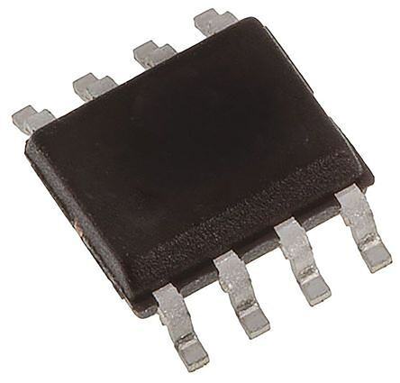
| 供应商器件封装 | 8-SOIC |
| 共模抑制比—最小值 | 70 dB |
| 包装 | 管件 |
| 压摆率 | 10 V/µs |
| 双重电源电压 | +/- 9 V, +/- 12 V, +/- 15 V |
| 商标 | Analog Devices |
| 增益带宽积 | - |
| 安装类型 | 表面贴装 |
| 安装风格 | SMD/SMT |
| 封装 | Tube |
| 封装/外壳 | 8-SOIC(0.154",3.90mm 宽) |
| 封装/箱体 | SOIC-8 |
| 工作温度 | -40°C ~ 85°C |
| 工作电源电压 | 6 V to 18 V |
| 工厂包装数量 | 98 |
| 放大器类型 | 音频 |
| 最大双重电源电压 | +/- 18 V |
| 最大工作温度 | + 85 C |
| 最小双重电源电压 | +/- 6 V |
| 最小工作温度 | - 40 C |
| 标准包装 | 98 |
| 电压-电源,单/双 (±) | ±6 V ~ 18 V |
| 电压-输入失调 | 50µV |
| 电流-电源 | 2.7mA |
| 电流-输入偏置 | - |
| 电流-输出/通道 | 45mA |
| 电源电压-最大 | 18 V |
| 电源电压-最小 | 6 V |
| 电源电流 | 2.7 mA |
| 电路数 | 1 |
| 类型 | Differential Line Receiver |
| 系列 | SSM2143 |
| 视频文件 | http://www.digikey.cn/classic/video.aspx?PlayerID=1364138032001&width=640&height=505&videoID=2245193153001http://www.digikey.cn/classic/video.aspx?PlayerID=1364138032001&width=640&height=505&videoID=2245193159001 |
| 输入电压范围—最大 | 18 V |
| 输入补偿电压 | 0.05 mV |
| 输出类型 | - |
| 通道数量 | 1 Channel |


- 商务部:美国ITC正式对集成电路等产品启动337调查
- 曝三星4nm工艺存在良率问题 高通将骁龙8 Gen1或转产台积电
- 太阳诱电将投资9.5亿元在常州建新厂生产MLCC 预计2023年完工
- 英特尔发布欧洲新工厂建设计划 深化IDM 2.0 战略
- 台积电先进制程称霸业界 有大客户加持明年业绩稳了
- 达到5530亿美元!SIA预计今年全球半导体销售额将创下新高
- 英特尔拟将自动驾驶子公司Mobileye上市 估值或超500亿美元
- 三星加码芯片和SET,合并消费电子和移动部门,撤换高东真等 CEO
- 三星电子宣布重大人事变动 还合并消费电子和移动部门
- 海关总署:前11个月进口集成电路产品价值2.52万亿元 增长14.8%


PDF Datasheet 数据手册内容提取
a –6 dB Differential Line Receiver SSM2143 FEATURES FUNCTIONAL BLOCK DIAGRAM High Common-Mode Rejection DC: 90 dB typ 60 Hz: 90 dB typ 12kW 6kW 20 kHz: 85 dB typ –IN SENSE Ultralow THD: 0.0006% typ @ 1 kHz V+ Fast Slew Rate: 10 V/(cid:109)s typ Wide Bandwidth: 7 MHz typ (G = 1/2) VOUT Two Gain Levels Available: G = 1/2 or 2 Low Cost V– 12kW 6kW +IN REFERENCE SSM2143 PIN CONNECTIONS Epoxy Mini-DIP (P Suffix) GENERAL DESCRIPTION and The SSM2143 is an integrated differential amplifier intended to SOIC (S Suffix) receive balanced line inputs in audio applications requiring a high level of immunity from common-mode noise. The device provides a typical 90 dB of common-mode rejection (CMR), REF 1 8 NC which is achieved by laser trimming of resistances to better than –IN 2 SSM2143 7 V+ 0.005%. TOP VIEW +IN 3 6 VOUT (NOT TO SCALE) Additional features of the device include a slew rate of 10 V/m s V– 4 5 SENSE and wide bandwidth. Total harmonic distortion (THD) is less OP-482 than 0.004% over the full audio band, even while driving low NC = NO CONNECT impedance loads. The SSM2143 input stage is designed to handle input signals as large as +28 dBu at G = 1/2. Although primarily intended for G = 1/2 applications, a gain of 2 can be realized by reversing the +IN/–IN and SENSE/REFERENCE connections. When configured for a gain of 1/2, the SSM2143 and SSM2142 Balanced Line Driver provide a fully integrated, unity gain solution to driving audio signals over long cable runs. For similar performance with G = 1, see SSM2141. REV.A Information furnished by Analog Devices is believed to be accurate and reliable. However, no responsibility is assumed by Analog Devices for its use, nor for any infringements of patents or other rights of third parties which may result from its use. No license is granted by implication or One Technology Way, P.O. Box 9106, Norwood, MA 02062-9106, U.S.A. otherwise under any patent or patent rights of Analog Devices. Tel: 617/329-4700 Fax: 781/461-3113
SSM2143–SPECIFICATIONS (V = (cid:54)15 V, –40(cid:56)C £ T £ +85(cid:56)C, G = 1/2, unless otherwise noted. S A Typical specifications apply at T = +25(cid:56)C) A Parameter Symbol Conditions Min Typ Max Units AUDIO PERFORMANCE Total Harmonic Distortion Plus Noise THD+N V = 10 V rms, R = 10 kW , f = 1 kHz 0.0006 % IN L Signal-to-Noise Ratio SNR 0 dBu = 0.775 V rms, 20 kHz BW, RTI –107.3 dBu Headroom HR Clip Point = 1% THD+N +28.0 dBu DYNAMIC RESPONSE Slew Rate SR R = 2 kW , C = 200 pF 6 10 V/m s L L Small Signal Bandwidth BW R = 2 kW , C = 200 pF –3 dB L L G = 1/2 7 MHz G = 2 3.5 MHz INPUT Input Offset Voltage V V = 0 V, RTI, G = 2 –1.2 0.05 +1.2 mV IOS CM Common-Mode Rejection CMR V = – 10 V, RTO CM f = dc 70 90 dB f = 60 Hz 90 dB f = 20 kHz 85 dB f = 400 kHz 60 dB Power Supply Rejection PSR V = – 6 V to – 18 V 90 110 dB S Input Voltage Range IVR Common Mode – 15 V Differential – 28 V OUTPUT Output Voltage Swing V R = 2 kW – 13 – 14 V O L Minimum Resistive Load Drive 2 kW Maximum Capacitive Load Drive 300 pF Short Circuit Current Limit I +45, –20 mA SC GAIN Gain Accuracy –0.1 0.03 0.1 % REFERENCE INPUT Input Resistance 18 kW Voltage Range – 10 V POWER SUPPLY Supply Voltage Range V – 6 – 18 V S Supply Current I V = 0 V, R = ¥ – 2.7 – 4.0 mA SY CM L Specifications subject to change without notice. ABSOLUTE MAXIMUM RATINGS Supply Voltage . . . . . . . . . . . . . . . . . . . . . . . . . . . . . . . .– 18 V Common-Mode Input Voltage . . . . . . . . . . . . . . . . . . . .– 22 V Differential Input Voltage . . . . . . . . . . . . . . . . . . . . . . .– 44 V Output Short Circuit Duration . . . . . . . . . . . . . . .Continuous Operating Temperature Range . . . . . . . . . . . . –40(cid:176) C to +85(cid:176) C Storage Temperature Range . . . . . . . . . . . . –65(cid:176) C to +150(cid:176) C Junction Temperature (T) . . . . . . . . . . . . . . . . . . . . +150(cid:176) C J Lead Temperature (Soldering, 60 sec) . . . . . . . . . . . . +300(cid:176) C Thermal Resistance 8-Pin Plastic DIP (P): q = 103, q = 43 . . . . . . . . . (cid:176) C/W JA JC 8-Pin SOIC (S): q = 150, q = 43. . . . . . . . . . . . . . (cid:176) C/W JA JC –2– REV. A
SSM2143 (cid:0)1ms (cid:0)100 100 (cid:0)90 90 (cid:0)10 10 (cid:0)0% 0% (cid:0)50mV 5V 5ms Figure 1.Small-Signal Transient Response (V = – 200 mV, Figure 2.Large Signal Transient Response (V = +24 dBu, IN IN G = 1/2, R = 2 kW , V = – 15 V, T = +25(cid:176)C) G = 1/2, R = 2 kW V = – 15 V, T = +25(cid:176)C) L S A L S A Figure 3.THD+N vs. Frequency (VS = – 15 V, Figure 4.Headroom (VS = – 15 V, RL = 10 kW , V = 10 V rms, with 80 kHz Filter) with 80 kHz Filter) IN 1.0 0.1 % – N 0.01 + D H T 0.001 0.0001 100 1k 10k 100k LOAD RESISTANCE – W Figure 5.Dynamic Intermodulation Distortion, DIM-100 Figure 6.THD+N vs. Load (V = – 15 V, V = 10 V rms, with S IN (V = – 15 V, R = 100 kW ) 1 kHz Sine, 80 kHz Filter) S L REV. A –3–
SSM2143 40 VS = ±15V 30 TA = +25°C B d– 20 VS = –15V N AI TA = +25(cid:176)C GP 10 O O LD- 0 E S O L–10 C –20 –30 100 1k 10k 100k 1M 10M FREQUENCY – Hz Figure 7.Closed-Loop Gain vs. Frequency, 20 Hz to 20 kHz Figure 8.Closed-Loop Gain vs. Frequency, 100 Hz to (Gain of 1/2 Normalized to 0 dB) 10 MHz 180 120 135 TVRASL === +±221k55W°VC dB100 TVAS == +±2155°VC 90 – N O se TI 80 e 45 C grDe– E ASHP–450 EEJRE DMON- 6400 O M –90 M O C 20 –135 –180 0 100 1k 10k 100k 1M 10M 100 1k 10k 100k 1M FREQUENCY – Hz FREQUENCY – Hz Figure 9.Closed-Loop Phase vs. Frequency Figure 10.Common-Mode Rejection vs. Frequency 140 10 VS = ±15V VS = ±15V Bd120 TA = +25°C TA = +25°C – 8 N O100 TICJEE 80 W – CEN 6 R A LYPPUSR 60 +PSRR –PSRR EDPIMT PU 4 WE 40 TU O O P 2 20 0 0 10 100 1k 10k 100k 1M 100 1k 10k 100k 1M FREQUENCY – Hz FREQUENCY – Hz Figure 11.Power Supply Rejection vs. Frequency Figure 12.Closed-Loop Output Impedance vs. Frequency –4– REV. A
SSM2143 6 12.5V msr V – 5 VRTGASL = === 1 ±+2/21k25W5V°C – V rms10.0V VTAS == +– 2155(cid:176)VC G 4 G N N IW WI 7.5V S S GE 3 GE A A T T LO OL 5.0V VT 2 T V U U P P UT UT 2.5V O 1 O 0 0V 1k 10k 100k 1M 10M 10 100 1k 10k FREQUENCY – Hz LOAD RESISTANCE – W Figure 13.Output Voltage Swing vs. Frequency Figure 14.Output Voltage Swing vs. Load Resistance 40 120 TA = +25(cid:176)C NG – V p–p 30 Hz V/ n – Y 18000 VTSA == ±+1255V°C OLTAGE SWI 20 TSINDEE SOI 60 V N OUTPUT 10 GEALTOV 2400 0 0 – 5 – 10 – 15 – 20 0 1 10 100 1k 10k SUPPLY VOLTAGE FREQUENCY – Hz Figure 15.Output Voltage Swing vs. Supply Voltage Figure 16.Voltage Noise Density vs. Frequency (cid:0)1s (cid:0)10ms (cid:0)100 (cid:0)100 (cid:0)90 (cid:0)90 0.5m V 5m V 0V 0V –0.5m V –5m V (cid:0)10 (cid:0)10 (cid:0)0% (cid:0)0% (cid:0)5mV (cid:0)5mV Figure 17.Low Frequency Voltage Noise from 0.1 Hz Figure 18.Voltage Noise from 0 kHz to 1 kHz* to 10 Hz* *The photographs in Figure 17 through Figure 19 were taken at V = – 15 V and T = +25(cid:176)C, using an external amplifier with a gain of 1000. S A REV. A –5–
SSM2143 16 VS = – 15V (cid:0)1ms R L = 2kW 14 (cid:0)100 (cid:0)90 s12 mV/ 5m V E – AT10 0V W R E –5m V SL 8 (cid:0)10 (cid:0)0% 6 (cid:0)5mV 4 –50 –25 0 25 50 75 100 TEMPERATURE – (cid:176)C Figure 19.Voltage Noise from 0 kHz to 10 kHz* Figure 20.Slew Rate vs. Temperature 0.10 400 VS = – 15V VS = – 15V VI N = – 10V 0.08 R S = 0W V m– 300 E % AG N ERROR – 00..0064 FSET VOLT 200 GAI T OF U P 100 0.02 IN 0 0 –50 –25 0 25 50 75 100 –50 –25 0 25 50 75 100 TEMPERATURE – (cid:176)C TEMPERATURE – (cid:176)C Figure 21.Gain Error vs. Temperature Figure 22.Input Offset Voltage vs. Temperature 5 4.0 VS = – 15V TA = +25°C 4 3.5 A A m m NT – 3 T–N 3.0 E E R R UR RU 2.5 C C Y 2 Y PPL LPP 2.0 U U S S 1 1.5 0 1.0 –50 –25 0 25 50 75 100 0 ±5 ±10 ±15 ±20 TEMPERATURE – (cid:176)C SUPPLY VOLTAGE – V Figure 23.Supply Current vs. Temperature Figure 24.Supply Current vs. Supply Voltage *The photographs in Figure 17 through Figure 19 were taken at V = – 15 V and T = +25(cid:176)C, using an external amplifier with a gain of 1000. S A –6– REV. A
SSM2143 APPLICATIONS INFORMATION Setting D R to 5 W results in the CMRR of 71 dB, as stated The SSM2143 is designed as a balanced differential line re- above. To achieve the SSM2143’s CMRR of 90 dB, the resistor ceiver. It uses a high speed, low noise audio amplifier with four mismatch can be at most 0.57 W . In other words, to build this precision thin-film resistors to maintain excellent common-mode circuit discretely, the resistors would have to be matched to rejection and ultralow THD. Figure 25 shows the basic differen- better than 0.005%! tial receiver application where the SSM2143 yields a gain of 1/2. The following table shows typical resistor accuracies and the The placement of the input and feedback resistors can be resulting CMRR for a differential amplifier. switched to achieve a gain of +2, as shown in Figure 26. For either circuit configuration, the SSM2143 can also be used un- % Mismatch CMRR balanced by grounding one of the inputs. In applications requir- 5% 30 dB ing a gain of +1, use the SSM2141. 1% 44 dB 0.1% 64 dB +15V +15V 0.1µF 0.1µF 0.005% 90 dB DC OUTPUT LEVEL ADJUST 12k 7 6k A V =12 6k 7 12k A V = 2 The reference node of the SSM2143 is normally connected to –IN 2 5 –IN 5 2 ground. However, it can be used to null out any dc offsets in SSM2143 + 6 SSM2143 6 the system or to introduce a dc reference level other than VOUT VOUT ground. As shown in Figure 28, the reference node needs to be 12k 6k 6k 12k +IN 3 1 +IN 1 3 +15V 4 4 0.1µF +10V 0.1µF 0.1µF OP27 –15V –15V 12k 7 6k –IN 2 5 –10V Figure 25.Standard Config- Figure 26.Reversing the uration for Gain of 1/2 Resistors Results in a SSM2143 6 VOUT Gain of 2 12k 6k REFERENCE +IN 3 1 CMRR 4 The internal thin-film resistors are precisely trimmed to achieve 0.1µF a CMRR of 90 dB. Any imbalances introduced by the external circuitry will cause a significant reduction in the overall CMRR –15V performance. For example, a 5 W source imbalance will result in Figure 28.A Low Impedance Buffer Is Required to Adjust a CMRR of 71 dB at dc. This is also true for any reactive source the Reference Voltage. impedances that may affect the CMRR over the audio frequency buffered with an op amp to maintain very low impedance to range. These error sources need to be minimized to maintain achieve high CMRR. The same reasoning as above applies such the excellent CMRR. that the 6 kW resistor has to be matched to better than 0.005% To quantify the required accuracy of the thin film resistor or 0.3 W . The op amp maintains very low output impedance matching, the source of CMRR error can be analyzed. A resistor over the entire audio frequency range, as long as its bandwidth mismatch can be modelled as shown in Figure 27. By assuming is well above 20 kHz. The reference input can be adjusted over a tolerance on one of the 12 kW resistors of D R, the equation for a – 10 V range. The gain from the reference to the output is the common-mode gain becomes: unity so the resulting dc output adjustment range is also – 10 V. VOUT = 6k (cid:230)(cid:231) 6k +1(cid:246)(cid:247) – 6k INPUT ERRORS V 6k+12kŁ 12k+D R ł 12k+D R The main dc input offset error specified for the SSM2143 is the IN Input Offset Voltage. The Input Bias Current and Input Offset which reduces to: Current are not specified as for a normal operational amplifier. Because the SSM2143 has built-in resistors, any bias current V 1/3D R OUT = related errors are converted into offset voltage errors. Thus, the VIN 12k+D R offset voltage specification is a combination of the amplifier’s offset voltage plus its offset current times the input impedance. This gain error leads to a common-mode rejection ratio of: |A | 18k +18V CMRR= DM @ ALL CABLE MEASUREMENTS USE +18V |A | DR BELDEN CABLE (500'). 0.1µF CM 6k 6 7 12k + D R VIN 4SSM21242 1 2SSM21435 6 VOUT –IN 8 4 12k VOUT 3 7 3 1 0.1µF +IN 5 18k 6k CMRR =D R –18V –18V Figure 27.A Small Mismatch in Resistance Results in a Figure 29. SSM2142/SSM2143 Balanced Line Driver/ Large Common-Mode Error Receiver System REV. A –7–
SSM2143 LINE DRIVER/RECEIVER SYSTEM of cable between the ICs as well as no cable. The combination The SSM2143 and SSM2142 provide a fully integrated line driver/ of the two parts results in excellent THD+N and SNR and a noise receiver system. The SSM2142 is a high performance balanced floor of typically –105 dB over a 20 Hz to 20 kHz bandwidth. line driver IC that converts an unbalanced input into a balanced A comment on SSM2142/SSM2143 system headroom is neces- output signal. It can drive large capacitive loads on long cables sary. Figure 31 shows a maximum signal handling of approximately making it ideal for transmitting balanced audio signals. When com- – 22 dBu, but it must be kept in mind that this is measured be- bined with an SSM2143 on the receiving end of the cable, the sys- tween the SSM2142’s input and SSM2143’s output, which has tem maintains high common-mode rejection and ultralow THD. been attenuated by one half. Normally, the system would be shown The SSM2142 is designed with a gain of +2 and the SSM2143 as actually used in a piece of equipment, whereby the SSM2143 is with a gain of 1/2, providing an overall system gain of unity. at the input and SSM2142 at the output. In this case, the system The following data demonstrates the typical performance of the could handle differential signals in excess of +24 dBu at the input two parts together, measured on an Audio Precision at the and output, which is consistent with headroom requirements of SSM2143’s output. This configuration was tested with 500 feet most professional audio equipment. 500' CABLE NO CABLE Figure 30.THD+N vs. Frequency of SSM2142/SSM2143 Figure 33.SSM2142/SSM2143 System Frequency System (VS = – 18 V, VIN = 5 V rms, with 80 kHz Filter) Response (VS = – 18 V, VIN = 0 dBV, 500' Cable) 5V 100 90 10 0% 10ms Figure 31. SSM2142/SSM2143 System Headroom– See Text—(V = – 18 V, R = 10 kW , 500' Cable) S L Figure 34. SSM2142/SSM2143 System Large Signal Pulse Response (VS = – 18 V, RL = 10 kW , No Cable) A. S. U. 500' CABLE N D I E T N RI P NO CABLE Figure 32.SSM2142/SSM2143 System DIM-100 Dynamic Intermodulation Distortion (V = – 18 V, R = 10 kW ) S L –8– REV. A
SSM2143 OUTLINE DIMENSIONS 0.400 (10.16) 0.365 (9.27) 0.355 (9.02) 8 5 0.280 (7.11) 0.250 (6.35) 1 4 0.240 (6.10) 0.325 (8.26) 0.310 (7.87) 0.100 (2.54) 0.300 (7.62) BSC 0.060 (1.52) 0.195 (4.95) 0.210 (5.33) MAX 0.130 (3.30) MAX 0.115 (2.92) 0.015 0.150 (3.81) (0.38) 0.015 (0.38) 0.130 (3.30) MIN GAUGE 0.115 (2.92) SEATING PLANE 0.014 (0.36) PLANE 0.010 (0.25) 0.022 (0.56) 0.008 (0.20) 0.005 (0.13) 0.430 (10.92) 0.018 (0.46) MIN MAX 0.014 (0.36) 0.070 (1.78) 0.060 (1.52) 0.045 (1.14) COMPLIANTTO JEDEC STANDARDS MS-001 CONTROLLING DIMENSIONSARE IN INCHES; MILLIMETER DIMENSIONS (RCINEOFRPEANRERERENN LCTEEHA EODSNSEL MSY)AAAYNR BDEE AR CROOEU NNNFODIGETUDAR-POEPFDRFOA INSPC RWHIAH ETOEQL UFEIO VORAR LU EHSNAETL ISFN FLDOEEARSDIGSN.. 070606-A Figure 35. 8-Lead Plastic Dual In-Line Package [PDIP] Narrow Body (N-8) Dimensions shown in inches and (millimeters) 5.00(0.1968) 4.80(0.1890) 8 5 4.00(0.1574) 6.20(0.2441) 3.80(0.1497) 1 4 5.80(0.2284) 1.27(0.0500) 0.50(0.0196) BSC 1.75(0.0688) 0.25(0.0099) 45° 0.25(0.0098) 1.35(0.0532) 8° 0.10(0.0040) 0° COPLANARITY 0.51(0.0201) 0.10 SEATING 0.31(0.0122) 0.25(0.0098) 10..2470((00..00510507)) PLANE 0.17(0.0067) COMPLIANTTOJEDECSTANDARDSMS-012-AA C(RINOEFNPEATRRREOENNLCLTEIHNEOGSNDELISYM)AEANNRDSEIAORRNOESUNANORDETEDAIN-POMPFRIFLOLMPIMIRLELIATIMTEEERTFSEO;RIRNECUQHSUEDIVIINMAELDENENSSTIIOGSNNFS.OR 012407-A Figure 36. 8-Lead Standard Small Outline Package [SOIC_N] Narrow Body (R-8) Dimensions shown in millimeters and (inches) REV. A –9–
SSM2143 ORDERING GUIDE Model1 Temperature Range Package Description Package Option SSM2143PZ −40°C to +85°C 8-Lead PDIP N-8 SSM2143SZ −40°C to +85°C 8-Lead SOIC_N R-8 SSM2143SZ-REEL −40°C to +85°C 8-Lead SOIC_N R-8 1 Z = RoHS Compliant Part REVISION HISTORY 6/11—Rev. 0 to Rev. A Updated Outline Dimensions ......................................................... 9 Changes to Ordering Guide .......................................................... 10 11/91—Revision 0: Initial Version ©1991–2011 Analog Devices, Inc. All rights reserved. Trademarks and registered trademarks are the property of their respective owners. D10010-0-6/11(A) –10– REV. A