ICGOO在线商城 > 集成电路(IC) > 线性 - 放大器 - 仪表,运算放大器,缓冲器放大器 > LMV651MFX/NOPB

 Datasheet下载
- 型号: LMV651MFX/NOPB
- 制造商: Texas Instruments
- 库位|库存: xxxx|xxxx
- 要求:
| 数量阶梯 | 香港交货 | 国内含税 |
| +xxxx | $xxxx | ¥xxxx |
查看当月历史价格
查看今年历史价格
LMV651MFX/NOPB产品简介:
ICGOO电子元器件商城为您提供LMV651MFX/NOPB由Texas Instruments设计生产,在icgoo商城现货销售,并且可以通过原厂、代理商等渠道进行代购。 LMV651MFX/NOPB价格参考¥3.22-¥7.98。Texas InstrumentsLMV651MFX/NOPB封装/规格:线性 - 放大器 - 仪表,运算放大器,缓冲器放大器, 通用 放大器 1 电路 满摆幅 SOT-23-5。您可以下载LMV651MFX/NOPB参考资料、Datasheet数据手册功能说明书,资料中有LMV651MFX/NOPB 详细功能的应用电路图电压和使用方法及教程。
LMV651MFX/NOPB 是 Texas Instruments(德州仪器)推出的一款低功耗、单通道轨到轨输入/输出运算放大器,属于线性 - 放大器 - 仪表、运算放大器、缓冲器放大器类别。其主要应用场景包括:

1. 电池供电设备:
   LMV651 的低静态电流(典型值为 270 nA)和低工作电压范围(1.8 V 至 5.5 V)使其非常适合用于便携式电池供电设备,例如手持式医疗设备、无线传感器节点和消费类电子产品。

2. 信号调理与放大:
   其轨到轨输入/输出特性允许在宽动态范围内精确处理小信号,适用于传感器信号调理、数据采集系统以及音频信号放大等场景。

3. 工业自动化与控制:
   在工业应用中,LMV651 可用于过程控制、数据监控和反馈回路中的信号放大与隔离。其高增益带宽积(1 MHz)和快速建立时间确保了系统的稳定性和响应速度。

4. 医疗电子设备:
   这款运放的低噪声性能(典型值为 9 µVrms)和高精度特性使其适合用于心率监测仪、血压计和其他需要高灵敏度信号处理的医疗设备。

5. 汽车电子系统:
   LMV651 的宽工作温度范围(-40°C 至 +125°C)和稳健的设计使其能够承受恶劣环境条件,适用于汽车传感器接口、车载信息娱乐系统以及电源管理电路。

6. 物联网 (IoT) 应用:
   在 IoT 领域,LMV651 的低功耗特性和紧凑封装(如 SOT-23 和 X2SON 封装)使其成为理想选择,可用于环境监测、智能家居设备和可穿戴技术。

总之,LMV651MFX/NOPB 凭借其低功耗、高性能和灵活性,广泛应用于各种需要小型化、高效能和高精度的电子系统中。
| 参数 | 数值 |
| -3db带宽 | - |
| 产品目录 | 集成电路 (IC)半导体 |
| 描述 | IC OPAMP GP 12MHZ RRO SOT23-5运算放大器 - 运放 12MHz Lo Vtg Lo Pwr Amp |
| 产品分类 | Linear - Amplifiers - Instrumentation, OP Amps, Buffer Amps集成电路 - IC |
| 品牌 | Texas Instruments |
| 产品手册 | |
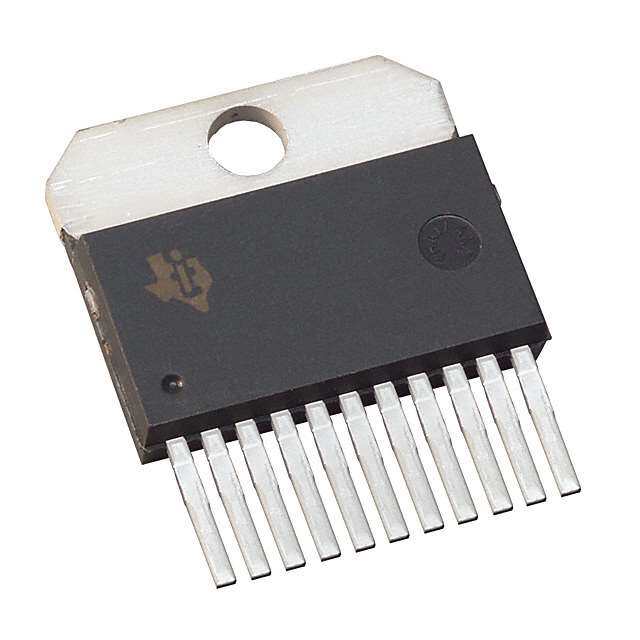
| 产品图片 |
|
| rohs | 符合RoHS无铅 / 符合限制有害物质指令(RoHS)规范要求 |
| 产品系列 | 放大器 IC,运算放大器 - 运放,Texas Instruments LMV651MFX/NOPB- |
| 数据手册 | |
| 产品型号 | LMV651MFX/NOPB |
| 产品种类 | 运算放大器 - 运放 |
| 供应商器件封装 | SOT-23-5 |
| 共模抑制比—最小值 | 90 dB |
| 关闭 | No Shutdown |
| 其它名称 | LMV651MFX/NOPBCT |
| 包装 | 剪切带 (CT) |
| 压摆率 | 3 V/µs |
| 商标 | Texas Instruments |
| 增益带宽生成 | 12 MHz |
| 增益带宽积 | 12MHz |
| 安装类型 | 表面贴装 |
| 安装风格 | SMD/SMT |
| 封装 | Reel |
| 封装/外壳 | SC-74A,SOT-753 |
| 封装/箱体 | SOT-23-5 |
| 工作温度 | -40°C ~ 125°C |
| 工作电源电压 | 2.7 V to 5.5 V |
| 工厂包装数量 | 3000 |
| 放大器类型 | 通用 |
| 最大工作温度 | + 125 C |
| 最小工作温度 | - 40 C |
| 标准包装 | 1 |
| 电压-电源,单/双 (±) | 2.7 V ~ 5.5 V |
| 电压-输入失调 | 100µV |
| 电流-电源 | 116µA |
| 电流-输入偏置 | 80nA |
| 电流-输出/通道 | 25mA |
| 电源电流 | 116 uA |
| 电路数 | 1 |
| 系列 | LMV651 |
| 设计资源 | http://www.digikey.com/product-highlights/cn/zh/texas-instruments-webench-design-center/3176 |
| 转换速度 | 3 V/us |
| 输入偏压电流—最大 | 120 nA |
| 输入补偿电压 | 1.5 mV |
| 输出电流 | 18.5 mA |
| 输出类型 | 满摆幅 |
| 通道数量 | 1 Channel |


- 商务部:美国ITC正式对集成电路等产品启动337调查
- 曝三星4nm工艺存在良率问题 高通将骁龙8 Gen1或转产台积电
- 太阳诱电将投资9.5亿元在常州建新厂生产MLCC 预计2023年完工
- 英特尔发布欧洲新工厂建设计划 深化IDM 2.0 战略
- 台积电先进制程称霸业界 有大客户加持明年业绩稳了
- 达到5530亿美元!SIA预计今年全球半导体销售额将创下新高
- 英特尔拟将自动驾驶子公司Mobileye上市 估值或超500亿美元
- 三星加码芯片和SET,合并消费电子和移动部门,撤换高东真等 CEO
- 三星电子宣布重大人事变动 还合并消费电子和移动部门
- 海关总署:前11个月进口集成电路产品价值2.52万亿元 增长14.8%


PDF Datasheet 数据手册内容提取
Product Sample & Technical Tools & Support & Folder Buy Documents Software Community LMV651,LMV652,LMV654 SNOSAI7K–SEPTEMBER2005–REVISEDMAY2016 LMV65x 12-MHz, Low Voltage, Low Power Amplifiers 1 Features 3 Description • Typical5-VSupply,UnlessOtherwiseNoted TI’s LMV65x devices are high-performance, low- 1 power operational amplifier ICs implemented with TI's • Specified3-Vand5-VPerformance advanced VIP50 process. This family of parts • LowPowerSupplyCurrent features 12 MHz of bandwidth while consuming only – LMV651:116 μA 116 μA of current, which is an exceptional bandwidth to power ratio in this operational amplifier class. The – LMV652:118 μAperAmplifier LMV65x devices are unity-gain stable and provide an – LMV654:122 μAperAmplifier excellent solution for general-purpose amplification in • HighUnity-GainBandwidth:12MHz low-voltage,low-powerapplications. • MaximumInputOffsetVoltage:1.5mV This family of low-voltage, low-power amplifiers • CMRR:100dB provides superior performance and economy in terms of power and space usage. These operational • PSRR:95dB amplifiers have a maximum input offset voltage of 1.5 • InputReferredVoltageNoise:17nV/√Hz mV, a rail-to-rail output stage, and an input common- • OutputSwingWith2-kΩ Load,120mVfromRail mode voltage range that includes ground. The LMV65x provide a PSRR of 95 dB, a CMRR of 100 • TotalHarmonicDistortion:0.003%at1kHz,2kΩ dB, and a total harmonic distortion (THD) of 0.003% • TemperatureRange:−40°Cto125°C at1-kHzfrequencyand2-kΩ load. 2 Applications The operating supply voltage range for this family of parts is from 2.7 V and 5.5 V. These operational • PortableEquipment amplifiers can operate over a wide temperature range • Automotive (−40°C to 125°C), making them ideal for automotive • Battery-PoweredSystems applications, sensor applications, and portable equipment applications. The LMV651 is offered in the • SensorsandInstrumentation ultra-tiny 5-pin SC70 and 5-pin SOT-23 package. The LMV652 is offered in an 8-pin VSSOP package. The LMV654isofferedina14-pinTSSOPpackage. DeviceInformation(1) PARTNUMBER PACKAGE BODYSIZE(NOM) SOT-23(5) 2.90mm×1.60mm LMV651 SC70(5) 2.00mm×1.25mm LMV652 VSSOP(8) 3.00mm×3.00mm LMV654 TSSOP(14) 5.00mm×4.40mm (1) For all available packages, see the orderable addendum at theendofthedatasheet. HighGainWideBandwidthInvertingAmplifier Open-LoopGainandPhasevsFrequency CF 120 120 100 100 R1 R2 PHASE CC1 1 k: 100 k: 80 80 VIN+- V+ RB1 +- CC2 +-VOUT )Bd( NIAG 4260000 GAIN 0426000 q)( ESAHP RB2 -20 + -20 V = 5V R2 -40 -40 AV = - R1= -100 100 1k 1F0RkEQ1U0E0NkCY 1(HMz) 10M 100M 1 An IMPORTANT NOTICE at the end of this data sheet addresses availability, warranty, changes, use in safety-critical applications, intellectualpropertymattersandotherimportantdisclaimers.PRODUCTIONDATA.
LMV651,LMV652,LMV654 SNOSAI7K–SEPTEMBER2005–REVISEDMAY2016 www.ti.com Table of Contents 1 Features.................................................................. 1 8 ApplicationandImplementation........................ 16 2 Applications........................................................... 1 8.1 ApplicationInformation............................................16 3 Description............................................................. 1 8.2 TypicalApplications................................................16 4 RevisionHistory..................................................... 2 8.3 DosandDon'ts.......................................................18 5 PinConfigurationandFunctions......................... 3 9 PowerSupplyRecommendations...................... 18 6 Specifications......................................................... 4 10 Layout................................................................... 19 6.1 AbsoluteMaximumRatings......................................4 10.1 LayoutGuidelines.................................................19 6.2 ESDRatings..............................................................4 10.2 LayoutExample....................................................19 6.3 RecommendedOperatingConditions.......................4 11 DeviceandDocumentationSupport................. 20 6.4 ThermalInformation..................................................4 11.1 DeviceSupport ....................................................20 6.5 3-VDCElectricalCharacteristics..............................5 11.2 DocumentationSupport .......................................20 6.6 5-VDCElectricalCharacteristics..............................6 11.3 RelatedLinks........................................................20 6.7 TypicalCharacteristics..............................................7 11.4 CommunityResources..........................................20 7 DetailedDescription............................................ 13 11.5 Trademarks...........................................................20 7.1 Overview.................................................................13 11.6 ElectrostaticDischargeCaution............................20 7.2 FunctionalBlockDiagram.......................................13 11.7 Glossary................................................................21 7.3 FeatureDescription.................................................13 12 Mechanical,Packaging,andOrderable Information........................................................... 21 7.4 DeviceFunctionalModes........................................14 4 Revision History NOTE:Pagenumbersforpreviousrevisionsmaydifferfrompagenumbersinthecurrentversion. ChangesfromRevisionJ(March2013)toRevisionK Page • AddedESDRatingstable,FeatureDescriptionsection,DeviceFunctionalModes,ApplicationandImplementation section,PowerSupplyRecommendationssection,Layoutsection,DeviceandDocumentationSupportsection,and Mechanical,Packaging,andOrderableInformationsection.................................................................................................. 1 ChangesfromRevisionI(March2012)toRevisionJ Page • ChangedlayoutofNationalDataSheettoTIformat........................................................................................................... 18 2 SubmitDocumentationFeedback Copyright©2005–2016,TexasInstrumentsIncorporated ProductFolderLinks:LMV651 LMV652 LMV654
LMV651,LMV652,LMV654 www.ti.com SNOSAI7K–SEPTEMBER2005–REVISEDMAY2016 5 Pin Configuration and Functions LMV651DBVorDCKPackage 5-PinSC70orSOT-23 LMV652DGKPackage TopView 8-PinVSSOP TopView LMV654PWPackage 14-PinTSSOP TopView PinFunctions:LMV651 PIN I/O DESCRIPTION NAME NO. –IN 3 I InvertingInput +IN 1 I NoninvertingInput OUT 4 O Output V– 2 P Negativesupplyinput V+ 5 P PositiveSupplyInput PinFunctions:LMV652,LMV654 PIN I/O DESCRIPTION NAME VSSOP TSSOP –INA 2 2 I Invertinginput,channelA +INA 3 3 I Noninvertinginput,channelA –INB 6 6 I Invertinginput,channelB +INB 5 5 I Noninvertinginput,channelB –INC — 9 I Invertinginput,channelC +INC — 10 I Noninvertinginput,channelC –IND — 13 I Invertinginput,channelD +IND — 12 I Noninvertinginput,channelD OUTA 1 1 O Output,channelA OUTB 7 7 O Output,channelB OUTC — 8 O Output,channelC OUTD — 14 O Output,channelD V– 4 11 P Negative(lowest)powersupply V+ 8 4 P Positive(highest)powersupply Copyright©2005–2016,TexasInstrumentsIncorporated SubmitDocumentationFeedback 3 ProductFolderLinks:LMV651 LMV652 LMV654
LMV651,LMV652,LMV654 SNOSAI7K–SEPTEMBER2005–REVISEDMAY2016 www.ti.com 6 Specifications 6.1 Absolute Maximum Ratings(1)(2) MIN MAX UNIT DifferentialinputV ±0.3 ID Supplyvoltage(V =V+-V−) 6 S Inputoroutputpinvoltage V−−0.3 V++0.3 V Infraredorconvection(20sec) 235 Solderinginformation °C Wavesolderingleadtemperature(10sec) 260 Junctiontemperature(3) 150 °C Storagetemperature,T −65 150 °C stg (1) StressesbeyondthoselistedunderAbsoluteMaximumRatingsmaycausepermanentdamagetothedevice.Thesearestressratings only,whichdonotimplyfunctionaloperationofthedeviceattheseoranyotherconditionsbeyondthoseindicatedunderRecommended OperatingConditions.Exposuretoabsolute-maximum-ratedconditionsforextendedperiodsmayaffectdevicereliability. (2) IfMilitary/Aerospacespecifieddevicesarerequired,pleasecontacttheTexasInstrumentsSalesOffice/Distributorsforavailabilityand specifications. (3) ThemaximumpowerdissipationisafunctionofT ,θ ,andT .Themaximumallowablepowerdissipationatanyambient J(MAX JA A temperatureisP =(T -T )/θ .AllnumbersapplyforpackagessoldereddirectlyontoaPCboard. D J(MAX) A JA 6.2 ESD Ratings VALUE UNIT Electrostatic Human-bodymodel(HBM)(1) ±2000 V V (ESD) discharge Machinemodel(2) ±100 (1) HumanBodyModel,applicablestd.MIL-STD-883,Method3015.7 (2) MachineModel,applicablestd.JESD22-A115-A(ESDMMstd.ofJEDEC)Field-InducedCharge-DeviceModel,applicablestd.JESD22- C101-C(ESDFICDMstd.ofJEDEC). 6.3 Recommended Operating Conditions MIN MAX UNIT Temperature −40 125 °C Supplyvoltage 2.7 5.5 V 6.4 Thermal Information LMV651 LMV652 LMV653 THERMALMETRIC(1) DCK DBV DGK PW UNIT (SC70) (SOT-23) (VSSOP) (TSSOP) 5PINS 5PINS 8PINS 14PINS R Junction-to-ambientthermalresistance 303.5 214.2 200.3 134.9 °C/W θJA R Junction-to-case(top)thermalresistance 135.5 173.3 89.1 60.9 °C/W θJC(top) R Junction-to-boardthermalresistance 81.1 72.5 120.9 77.3 °C/W θJB ψ Junction-to-topcharacterizationparameter 8.4 56.7 21.7 11.5 °C/W JT ψ Junction-to-boardcharacterizationparameter 80.4 71.9 119.4 76.7 °C/W JB R Junction-to-case(bottom)thermalresistance n/a n/a n/a n/a °C/W θJC(bot) (1) Formoreinformationabouttraditionalandnewthermalmetrics,seetheSemiconductorandICPackageThermalMetricsapplication report,SPRA953. 4 SubmitDocumentationFeedback Copyright©2005–2016,TexasInstrumentsIncorporated ProductFolderLinks:LMV651 LMV652 LMV654
LMV651,LMV652,LMV654 www.ti.com SNOSAI7K–SEPTEMBER2005–REVISEDMAY2016 6.5 3-V DC Electrical Characteristics Unlessotherwisespecified,alllimitsarespecifiedforT =25°C,V+=3V,V−=0V,V =V =V+/2,andR >1MΩ. A O CM L PARAMETER TESTCONDITIONS MIN(1) TYP(2) MAX(1) UNIT 0.1 ±1.5 VOS Inputoffsetvoltage mV Overspecifiedtemperaturerange 2.7 TCVOS Inputoffsetaveragedrift 6.6 μV/°C IB Inputbiascurrent(3) 80 120 nA IOS Inputoffsetcurrent 2.2 15 nA 87 100 CMRR Common-moderejectionratio 0≤VCM≤2V dB Overspecifiedtemperaturerange 80 87 95 3≤V+≤5V,VCM=0.5 Overspecifiedtemperaturerange 81 PSRR Powersupplyrejectionratio dB 2.7≤V+≤5.5V, 87 95 VCM=0.5 Overspecifiedtemperaturerange 81 Inputcommon-modevoltage CMRR≥75dB 0 2.1 CMVR V range CMRR≥60dB,overspecifiedtemperaturerange 0 2.1 0.3≤VO≤2.7,RL=2kΩtoV+/2 80 85 0.4≤VO≤2.6,RL=2kΩtoV+/2,overspecifiedtemperaturerange 76 AVOL Largesignalvoltagegain 0.3≤VO≤2.7,RL=10kΩtoV+/2 86 93 dB 0.4≤VO≤2.6,RL=10kΩtoV+/2,overspecifiedtemperature 83 range 80 95 RL=2kΩtoV+/2 Overspecifiedtemperaturerange 120 Outputswinghigh 45 50 RL=10kΩtoV+/2 Overspecifiedtemperaturerange 60 mVfrom VO 95 110 rail RL=2kΩtoV+/2 Overspecifiedtemperaturerange 125 Outputswinglow 60 65 RL=10kΩtoV+/2 Overspecifiedtemperaturerange 75 Maximumcontinuousoutput Sourcing(4) 17 ISC current Sinking(4) 25 mA 115 140 LMV651 Overspecifiedtemperaturerange 175 118 140 IS Supplycurrentperamplifier LMV652 μA Overspecifiedtemperaturerange 175 122 140 LMV654 Overspecifiedtemperaturerange 175 SR Slewrate AV=+1,10%to90%(5) 3.0 V/μs GBW Gainbandwidthproduct 12 MHz f=100kHz 17 en Input-referredvoltagenoise nV/√Hz f=1kHz 17 f=100kHz 0.1 in Input-referredcurrentnoise pA/√Hz f=1kHz 0.15 THD Totalharmonicdistortion f=1kHz,AV=2,RL=2kΩ 0.003% (1) Limitsare100%productiontestedat25°C.Limitsovertheoperatingtemperaturerangearespecifiedthroughcorrelationsusing StatisticalQualityControl(SQC)method. (2) Typicalvaluesrepresentthemostlikelyparametricnormasdeterminedatthetimeofcharacterization.Actualtypicalvaluesmayvary overtimeandwillalsodependontheapplicationandconfiguration.Thetypicalvaluesarenottestedandarenotensuredonshipped productionmaterial. (3) Positivecurrentcorrespondstocurrentflowingintothedevice. (4) Slewrateistheaverageoftherisingandfallingslewrates. (5) Thepartisnotshort-circuitprotectedandisnotrecommendedforoperationwithlowresistiveloads.Typicalsourcingandsinkingoutput currentcurvesareprovidedinTypicalCharacteristicsandshouldbeconsultedbeforedesigningforheavyloads. Copyright©2005–2016,TexasInstrumentsIncorporated SubmitDocumentationFeedback 5 ProductFolderLinks:LMV651 LMV652 LMV654
LMV651,LMV652,LMV654 SNOSAI7K–SEPTEMBER2005–REVISEDMAY2016 www.ti.com 6.6 5-V DC Electrical Characteristics Unlessotherwisespecified,alllimitsarespecifiedforT =25°C,V+=5V,V−=0V,V =V =V+/2,andR >1MΩ. J O CM L PARAMETER TESTCONDITIONS MIN(1) TYP(2) MAX(1) UNIT 0.1 ±1.5 VOS Inputoffsetvoltage mV Overspecifiedtemperaturerange 2.7 TCVOS Inputoffsetaveragedrift 6.6 μV/°C IB Inputbiascurrent See(3) 80 120 nA IOS Inputoffsetcurrent 2.2 15 nA 90 100 CMRR Common-moderejectionratio 0≤VCM≤4V dB Overspecifiedtemperaturerange 83 87 95 3V≤V+≤5V,VCM=0.5V Overspecifiedtemperaturerange 81 PSRR Powersupplyrejectionratio dB 2.7V≤V+≤5.5V,VCM= 87 95 0.5V Overspecifiedtemperaturerange 81 Inputcommon-modevoltage CMRR≥80dB 0 4.1 CMVR V range CMRR≥68dB,overspecifiedtemperaturerange 0 4.1 0.3≤VO≤4.7V,RL=2kΩtoV+/2 79 84 0.4≤VO≤4.6V,RL=2kΩtoV+/2,overspecifiedtemperaturerange 76 AVOL Largesignalvoltagegain 0.3≤VO≤4.7V,RL=10kΩtoV+/2 87 94 dB 0.4≤VO≤4.6V,RL=10kΩtoV+/2,overspecifiedtemperature 84 range 120 140 RL=2kΩtoV+/2 Overspecifiedtemperaturerange 185 Outputswinghigh 75 90 RL=10kΩtoV+/2 Overspecifiedtemperaturerange 120 mVfrom VO 110 130 rail RL=2kΩtoV+/2 Overspecifiedtemperaturerange 150 Outputswinglow 70 80 RL=10kΩtoV+/2 Overspecifiedtemperaturerange 95 Maximumcontinuousoutput Sourcing(4) 18.5 ISC current Sinking(4) 25 mA 116 140 LMV651 Overspecifiedtemperaturerange 175 118 140 IS Supplycurrentperamplifier LMV652 μA Overspecifiedtemperaturerange 175 122 140 LMV654 Overspecifiedtemperaturerange 175 SR Slewrate AV=+1,VO=1VPP,10%to90%(5) 3.0 V/μs GBW Gainbandwidthproduct 12 MHz f=100kHz 17 en Input-referredvoltagenoise nV/√Hz f=1kHz 17 f=100kHz 0.1 in Input-referredcurrentnoise pA/√Hz f=1kHz 0.15 THD Totalharmonicdistortion f=1kHz,AV=2,RL=2kΩ 0.003% (1) Limitsare100%productiontestedat25°C.Limitsovertheoperatingtemperaturerangearespecifiedthroughcorrelationsusing StatisticalQualityControl(SQC)method. (2) Typicalvaluesrepresentthemostlikelyparametricnormasdeterminedatthetimeofcharacterization.Actualtypicalvaluesmayvary overtimeandwillalsodependontheapplicationandconfiguration.Thetypicalvaluesarenottestedandarenotensuredonshipped productionmaterial. (3) Positivecurrentcorrespondstocurrentflowingintothedevice. (4) Thepartisnotshort-circuitprotectedandisnotrecommendedforoperationwithlowresistiveloads.Typicalsourcingandsinkingoutput currentcurvesareprovidedinTypicalCharacteristicsandshouldbeconsultedbeforedesigningforheavyloads. (5) Slewrateistheaverageoftherisingandfallingslewrates. 6 SubmitDocumentationFeedback Copyright©2005–2016,TexasInstrumentsIncorporated ProductFolderLinks:LMV651 LMV652 LMV654
LMV651,LMV652,LMV654 www.ti.com SNOSAI7K–SEPTEMBER2005–REVISEDMAY2016 6.7 Typical Characteristics Unlessotherwisespecified,T =25°C,V =5V,V+=5V,V−=0V,V =V /2 A S CM S 180 180 125°C 125°C 160 160 140 140 )A )A 25°C P P ( S 25°C ( S I 120 I 120 -40°C -40°C 100 100 80 80 2.7 3.2 3.7 4.2 4.7 5.25.5 2.7 3.2 3.7 4.2 4.7 5.25.5 VS (V) VS (V) Figure1.SupplyCurrentvsSupplyVoltage(LMV651) Figure2.SupplyCurrentperChannelvsSupplyVoltage (LMV652) 180 1 0.75 160 125°C 125°C 0.5 0.25 )A 140 25°C )Vm ( PS ( SO 0 25°C I 120 V -0.25 -40°C -40°C -0.5 100 -0.75 VS = 3V 80 -1 2.7 3.2 3.7 4.2 4.7 5.25.5 0 0.5 1 1.5 2 2.5 VS (V) VCM (V) Figure3.SupplyCurrentperChannelvsSupplyVoltage Figure4.V vsV OS CM (LMV654) 1 1 0.75 0.75 125°C 125°C 0.5 0.5 0.25 0.25 )V )V m m ( S 0 25°C ( S 0 O O 25°C V -0.25 V -0.25 -40°C -0.5 -0.5 -40°C -0.75 -0.75 VS = 5V -1 -1 0 1 2 3 4 5 2.7 3.2 3.7 4.2 4.7 5.2 5.5 VCM (V) VS (V) Figure5.V vsV Figure6.V vsSupplyVoltage OS CM OS Copyright©2005–2016,TexasInstrumentsIncorporated SubmitDocumentationFeedback 7 ProductFolderLinks:LMV651 LMV652 LMV654
LMV651,LMV652,LMV654 SNOSAI7K–SEPTEMBER2005–REVISEDMAY2016 www.ti.com Typical Characteristics (continued) Unlessotherwisespecified,T =25°C,V =5V,V+=5V,V−=0V,V =V /2 A S CM S 100 100 125°C 90 90 125°C )A 80 )A 80 n n ( SA 25°C ( SA IIB 70 IIB 70 -40°C 25°C -40°C 60 60 VS = 3V VS = 5V 50 50 0 0.5 1 1.5 2 2.5 0 1 2 3 4 5 VCM (V) VCM (V) Figure7.I vsV Figure8.I vsV BIAS CM BIAS CM 100 150 125°C 90 120 125°C )V m ( L )A 80 IA 90 n R ( S 25°C M A O 25°C IIB 70 RF 60 -40°C T -40°C U O V 60 30 RL = 2 k: 50 0 2.7 3.2 3.7 4.2 4.7 5.25.5 3 3.4 3.8 4.2 4.6 5 VS (V) VS (V) Figure9.IBIASvsSupplyVoltage Figure10.PositiveOutputSwingvsSupplyVoltage 150 100 125°C 125°C 120 80 )V )V m m ( L ( L IA 90 IA 60 R R M 25°C M O -40°C O RF 60 RF 40 25°C T T UO UO -40°C V V 30 20 RL = 2 k: RL = 10 k: 0 0 3 3.4 3.8 4.2 4.6 5 3 3.4 3.8 4.2 4.6 5 VS (V) VS (V) Figure11.NegativeOutputSwingvsSupplyVoltage Figure12.PositiveOutputSwingvsSupplyVoltage 8 SubmitDocumentationFeedback Copyright©2005–2016,TexasInstrumentsIncorporated ProductFolderLinks:LMV651 LMV652 LMV654
LMV651,LMV652,LMV654 www.ti.com SNOSAI7K–SEPTEMBER2005–REVISEDMAY2016 Typical Characteristics (continued) Unlessotherwisespecified,T =25°C,V =5V,V+=5V,V−=0V,V =V /2 A S CM S 90 30 125°C VS = 5V 75 25 25°C )V m -40°C ( L 60 )A 20 IA m R M 45 25°C ( EC 15 O -40°C R RF T 30 IUOS 10 125°C U O V 15 5 RL = 10 k: 0 0 0 0.25 0.5 0.75 1 1.25 1.5 3 3.4 3.8 4.2 4.6 5 VS (V) VOUT FROM RAIL (V) Figure13.NegativeOutputSwingvsSupplyVoltage Figure14.SourcingCurrentvsOutputVoltage 50 50 VS = 5V VS = 5V -40°C -40°C 40 40 25°C 25°C )A 30 )A 30 m m 125°C ( K 125°C ( K N N IS 20 IS 20 I I 10 10 0 0 0 0.05 0.1 0.15 0.2 0.25 0.3 0.35 0.4 0 0.05 0.1 0.15 0.2 0.25 0.3 0.35 0.4 0.45 VOUT FROM RAIL (V) VOUT FROM RAIL (V) Figure15.SinkingCurrentvsOutputVoltage(LMV651) Figure16.SinkingCurrentvsOutputVoltage(LMV652) 50 180 180 VS = 5V RL = 2 k: -40°C 150 150 PHASE 40 120 120 25°C )Am( IKNIS 2300 125°C )Bd( NIAG 639000 GAIN CL = 1C0L0 =p F50 pF CL = 20 pF 639000 °) E(SAHP 0 0 10 CL = 100 pF -30 -30 CL = 50 pF 0 -60 -60 0 0.1 0.2 0.3 0.4 0.5 100 1k 10k 100k 1M 10M 100M VOUT FROM RAIL (V) FREQUENCY (Hz) Figure17.SinkingCurrentvsOutputVoltage(LMV654) Figure18.Open-LoopGainandPhaseWithCapacitiveLoad Copyright©2005–2016,TexasInstrumentsIncorporated SubmitDocumentationFeedback 9 ProductFolderLinks:LMV651 LMV652 LMV654
LMV651,LMV652,LMV654 SNOSAI7K–SEPTEMBER2005–REVISEDMAY2016 www.ti.com Typical Characteristics (continued) Unlessotherwisespecified,T =25°C,V =5V,V+=5V,V−=0V,V =V /2 A S CM S 180 180 60 CL = 20 pF RL = 2 k: 150 150 PHASE 50 120 120 )Bd( N 6900 RL = 10:RL = 2 k: 6900 )°( ES )°( NIGRA 4300 IAG 30 GAIN 30 AHP M ES VS = 5V RL = 2 k: AH 20 0 0 P VS = 3V 10 -30 -30 -60 -60 0 100 1k 10k 100k 1M 10M 100M 10 100 1000 FREQUENCY (Hz) CL (pF) Figure19.Open-LoopGainandPhaseWithResistiveLoad Figure20.PhaseMarginvsCapacitiveLoad(Stability) 100 10 E E S SIO ION N E TN G E A R 1 T R LOV DERREFER TUPNI HZ)(nV/ 10 UC DERREFER TUPNI HZ)(pA/ 0.10 1 0.01 1 10 100 1k 10k 100k 1 10 100 1k 10k 100k FREQUENCY (Hz) FREQUENCY (Hz) Figure21.Input-ReferredVoltageNoisevsFrequency Figure22.Input-ReferredCurrentNoisevsFrequency 4 1 3.5 3 0.1 )s/V( ETAP 2.25 RISING )%( N+ 0.01 RL = 2 k: R FALLING D W 1.5 HT EL RL = 100 k: S 1 0.001 VS = 3V 0.5 VIN = 1 kHz SINE WAVE AV = +2 0 0.0001 3 3.5 4 4.5 5 0.001 0.01 0.1 1 10 VS (V) VOUT (V) Figure23.SlewRatevsSupplyVoltage Figure24.THD+NvsVOUT 10 SubmitDocumentationFeedback Copyright©2005–2016,TexasInstrumentsIncorporated ProductFolderLinks:LMV651 LMV652 LMV654
LMV651,LMV652,LMV654 www.ti.com SNOSAI7K–SEPTEMBER2005–REVISEDMAY2016 Typical Characteristics (continued) Unlessotherwisespecified,T =25°C,V =5V,V+=5V,V−=0V,V =V /2 A S CM S 1 1 VS = 3V VIN = 1 VPP AV = +2 0.1 0.1 )% )% ( N+D RL = 2 k: ( N+D HT RL = 100 k: HT RL = 2 k: 0.01 0.01 VS = 5V VIN = 1 kHz SINE WAVE AV = +2 RL = 100 k: 0.001 0.001 0.001 0.01 0.1 1 10 10 100 1k 10k 100k VOUT (V) FREQUENCY (Hz) Figure25.THD+NvsV Figure26.THD+NvsFrequency OUT 0.1 30 VS = 5V VS = 5V 25 VIN = 2 VPP CL = 15 pF, AV = +1 AV = +2 20 VIN = 20 mVPP, 20 kHz RL = 2 k: 15 0.01 )% )V 10 ( N+DHT RL = 100 k: m( VTUO 05 0.001 -5 -10 -15 0.0001 -20 10 100 1k 10k 100k 0 20 40 60 80 100 TIME (Ps) FREQUENCY (Hz) Figure27.THD+NvsFrequency Figure28.SmallSignalTransientResponse 30 1.5 25 20 1 15 10 0.5 )Vm 5 )Vm VS = 5V ( TU 0 ( TU 0 CL = 15 pF, AV = +1 OV -5 VO VIN = 2 VPP, 20 kHz -10 -0.5 -15 VS = 5V -20 CL = 125 pF, AV = +1 -1 -25 VIN = 20 mVPP, 20 kHz -30 -1.5 0 20 40 60 70 80 0 20 40 60 80 100 TIME (Ps) TIME (Ps) Figure29.SmallSignalTransientResponse Figure30.LargeSignalTransientResponse Copyright©2005–2016,TexasInstrumentsIncorporated SubmitDocumentationFeedback 11 ProductFolderLinks:LMV651 LMV652 LMV654
LMV651,LMV652,LMV654 SNOSAI7K–SEPTEMBER2005–REVISEDMAY2016 www.ti.com Typical Characteristics (continued) Unlessotherwisespecified,T =25°C,V =5V,V+=5V,V−=0V,V =V /2 A S CM S 120 120 VS = 5V, +PSRR VS = 3V, +PSRR 100 100 VS = 5V, -PSRR 80 80 )B )B d( R 60 VS = 3V, -PSRR d( R 60 R R S M P C 40 40 20 20 0 0 10 100 1k 10k 100k 1M 10M 10 100 1k 10k 100k 1M FREQUENCY (Hz) FREQUENCY (Hz) Figure31.PSRRvsFrequency Figure32.CMRRvsFrequency 1000 100 )W 10 ( T U O Z 1 0.1 0.01 10 100 1k 10k 100k 1M 10M 100M FREQUENCY (Hz) Figure33.Closed-LoopOutputImpedancevsFrequency 12 SubmitDocumentationFeedback Copyright©2005–2016,TexasInstrumentsIncorporated ProductFolderLinks:LMV651 LMV652 LMV654
LMV651,LMV652,LMV654 www.ti.com SNOSAI7K–SEPTEMBER2005–REVISEDMAY2016 7 Detailed Description 7.1 Overview TI’s LMV65x devices have 12 MHz of bandwidth, are unity-gain stable, and consume only 116 μA of current. They also have a maximum input offset voltage of 1.5 mV, a rail-to-rail output stage, and an input common-mode voltage range that includes ground. Lastly, these operational amplifiers provide a PSRR of 95 dB, a CMRR of 100dB,andatotalharmonicdistortion(THD)of0.003%at1-kHzfrequencyand2-kΩload. 7.2 Functional Block Diagram (EachAmplifier) 7.3 Feature Description 7.3.1 LowVoltageandLowPowerOperation The LMV65x have performance specified at supply voltages of 3 V and 5 V. These parts are specified to be operational at all supply voltages between 2.7 V and 5.5 V. The LMV651 draws a low supply current of 116 μA, the LMV652 draws 118 μA/channel and the LMV654 draws 122 μA/channel. This family of operational amplifiers providesthelowvoltageandlowpoweramplificationthatisessentialforportableapplications. 7.3.2 WideBandwidth Despite drawing the very low supply current of 116 µA, the LMV65x manage to provide a wide unity-gain bandwidth of 12 MHz. This is easily one of the best bandwidth to power ratios ever achieved, and allows these operational amplifiers to provide wideband amplification while using the minimum amount of power. This makes this family of parts ideal for low-power signal processing applications such as portable media players and other accessories. 7.3.3 LowInputReferredNoise The LMV65x provides a flatband input referred voltage noise density of 17 nV/√Hz, which is significantly better than the noise performance expected from a low-power operational amplifiers. These operational amplifiers also feature exceptionally low 1/f noise, with a very low 1/f noise corner frequency of 4 Hz. This makes these parts idealforlowpowerapplicationswhichrequiredecentnoiseperformance,suchasPDAsandportablesensors. 7.3.4 GroundSensingandRail-to-RailOutput The LMV65x each have a rail-to-rail output stage, which provides the maximum possible output dynamic range. This is especially important for applications requiring a large output swing. The input common-mode range of this family of devices includes the negative supply rail which allows direct sensing at ground in a single-supply operation. 7.3.5 SmallSize The small footprint of the packages for the LMV65x saves space on printed-circuit boards, and enables the design of smaller and more compact electronic products. Long traces between the signal source and the operational amplifier make the signal path susceptible to noise. By using a physically smaller package, these operational amplifiers can be placed closer to the signal source, reducing noise pickup and enhancing signal integrity. Copyright©2005–2016,TexasInstrumentsIncorporated SubmitDocumentationFeedback 13 ProductFolderLinks:LMV651 LMV652 LMV654
LMV651,LMV652,LMV654 SNOSAI7K–SEPTEMBER2005–REVISEDMAY2016 www.ti.com 7.4 Device Functional Modes 7.4.1 StabilityandCapacitiveLoading If the phase margin of the LMV65x is plotted with respect to the capacitive load (C ) at its output, it is seen that L the phase margin reduces significantly if C is increased beyond 100 pF. This is because the operational L amplifier is designed to provide the maximum bandwidth possible for a low supply current. Stabilizing it for higher capacitive loads would have required either a drastic increase in supply current, or a large internal compensation capacitance,whichwouldhavereducedthebandwidthoftheoperationalamplifier.Hence,ifthesedevicesareto beusedfordrivinghighercapacitiveloads,theywouldhavetobeexternallycompensated. N AI G STABLE ROC – 20 dB/decade UNSTABLE ROC = 40 dB/decade 0 FREQUENCY (Hz) Figure34. GainvsFrequencyforanOperationalAmplifiers An operational amplifier, ideally, has a dominant pole close to DC, which causes its gain to decay at the rate of 20 dB/decade with respect to frequency. If this rate of decay, also known as the rate of closure (ROC), remains the same until the unity-gain bandwidth of the operational amplifiers is stable. If, however, a large capacitance is added to the output of the operational amplifier, it combines with the output impedance of the operational amplifier to create another pole in its frequency response before its unity-gain frequency (see Figure 34). This increasestheROCto40dB/decadeandcausesinstability. In such a case a number of techniques can be used to restore stability to the circuit. The idea behind all these schemes is to modify the frequency response such that it can be restored to an ROC of 20 dB/decade, which ensuresstability. 7.4.2 InTheLoopCompensation Figure 35 illustrates a compensation technique, known as in-the-loop compensation, that employs an RC feedback circuit within the feedback loop to stabilize a noninverting amplifier configuration. A small series resistance, R , is used to isolate the amplifier output from the load capacitance, C , and a small capacitance, C , S L F isinsertedacrossthefeedbackresistortobypassC athigherfrequencies. L VIN + ROUT RS - CL RL CF RF RIN Figure35. In-the-LoopCompensation 14 SubmitDocumentationFeedback Copyright©2005–2016,TexasInstrumentsIncorporated ProductFolderLinks:LMV651 LMV652 LMV654
LMV651,LMV652,LMV654 www.ti.com SNOSAI7K–SEPTEMBER2005–REVISEDMAY2016 Device Functional Modes (continued) ThevaluesforR andC aredecidedbyensuringthatthezeroattributedtoC liesatthesamefrequencyasthe S F F pole attributed to C . This ensures that the effect of the second pole on the transfer function is compensated for L by the presence of the zero, and that the ROC is maintained at 20 dB/decade. For the circuit shown in Figure 35 the values of R and C are given by Equation 1. Values of R and C required for maintaining stability for S F S F different values of C , as well as the phase margins obtained, are shown in Table 1. R and R are taken to be L F IN 10kΩ,R is2kΩ,whileR istakenas340Ω. L OUT RS = ROUTRIN RF ¤§RF + 2RIN¤' CF = ¤' RF2 ¤§CLROUT (1) Table1.LoopCompensationValues C (pF) R (Ω) C (pF) PHASEMARGIN(°) L S F 150 340 15 39.4 200 340 20 34.6 250 340 25 31.1 Although this methodology provides circuit stability for any load capacitance, it does so at the price of bandwidth. Theclosed-loopbandwidthofthecircuitisnowlimitedbyR andC . F F 7.4.3 CompensationByExternalResistor In some applications, it is essential to drive a capacitive load without sacrificing bandwidth. In such a case, in the loop compensation is not viable. A simpler scheme for compensation is shown in Figure 36. A resistor, R , is ISO placed in series between the load capacitance and the output. This introduces a zero in the circuit transfer function, which counteracts the effect of the pole formed by the load capacitance, and ensures stability. The value of R to be used should be decided depending on the size of C and the level of performance desired. ISO L Values ranging from 5 Ω to 50 Ω are usually sufficient to ensure stability. A larger value of R results in a ISO system with lesser ringing and overshoot, but it also limits the output swing and the short-circuit current of the circuit. Figure36. CompensationbyIsolationResistor Copyright©2005–2016,TexasInstrumentsIncorporated SubmitDocumentationFeedback 15 ProductFolderLinks:LMV651 LMV652 LMV654
LMV651,LMV652,LMV654 SNOSAI7K–SEPTEMBER2005–REVISEDMAY2016 www.ti.com 8 Application and Implementation NOTE Information in the following applications sections is not part of the TI component specification, and TI does not warrant its accuracy or completeness. TI’s customers are responsible for determining suitability of components for their purposes. Customers should validateandtesttheirdesignimplementationtoconfirmsystemfunctionality. 8.1 Application Information With a low supply current, low power operation, and low harmonic distortion, the LMV65x devices are ideal for wide-bandwidth,highgainamplification. 8.2 Typical Applications 8.2.1 HighGain,LowPowerInvertingAmplifiers CF R1 R2 CC1 1 k: 100 k: + VIN - CC2 - + + V+ RB1 -VOUT RB2 R2 AV = - R1= -100 Figure37. HighGainInvertingAmplifier 8.2.1.1 DesignRequirements The wide unity-gain bandwidth allows these parts to provide large gain over a wide frequency range, while drivingloadsaslowas2kΩ withlessthan0.003%distortion. 8.2.1.2 DetailedDesignProcedure Figure 37 is an inverting amplifier, with a 100-kΩ feedback resistor, R , and a 1-kΩ input resistor, R , and 2 1 provides a gain of −100. With the LMV65x, these circuits can provide gain of −100 with a −3-dB bandwidth of 120 kHz, for a quiescent current as low as 116 μA. Coupling capacitors C and C can be added to isolate the C1 C2 circuit from DC voltages, while R and R provide DC biasing. A feedback capacitor C can also be added to B1 B2 F improvecompensation. 16 SubmitDocumentationFeedback Copyright©2005–2016,TexasInstrumentsIncorporated ProductFolderLinks:LMV651 LMV652 LMV654
LMV651,LMV652,LMV654 www.ti.com SNOSAI7K–SEPTEMBER2005–REVISEDMAY2016 Typical Applications (continued) 8.2.1.3 ApplicationCurve e e d u plit m A al n g Si Vout (1V/div) Vin (10mV/div) 0 50 100 150 200 Time (us) C001 Figure38. HighGainInvertingAmplifierResults 8.2.2 HighGain,LowPowerNoninvertingAmplifiers With a low supply current, low power operation, and low harmonic distortion, the LMV65x devices are ideal for wide-bandwidth, high gain amplification. The wide unity-gain bandwidth allows these parts to provide large gain over a wide frequency range, while driving loads as low as 2 kΩ with less than 0.003% distortion. Figure 39 is a noninverting amplifier with a gain of 1001, can provide that gain with a −3-dB bandwidth of 12 kHz, for a similar low quiescent power dissipation. With the LMV65x, these circuits can provide gain of −100 with a −3-dB bandwidth of 120 kHz, for a quiescent current as low as 116 μA. Coupling capacitors C and C can be added C1 C2 to isolate the circuit from DC voltages, while R and R provide DC biasing. A feedback capacitor C can also B1 B2 F beaddedtoimprovecompensation. + V RB1 CC2 + + VIN- RB2 -1 RM2: +-VOUT R1 CF 1 k: CC1 AV = 1 +R2= 1001 R1 Figure39. HighGainNoninvertingAmplifier 8.2.3 ActiveFilters With a wide unity-gain bandwidth of 12 MHz, low input-referred noise density, and a low power supply current, the LMV65x devices are well suited for low-power filtering applications. Active filter topologies, like the Sallen- Key low-pass filter shown in Figure 40, are very versatile, and can be used to design a wide variety of filters (Chebyshev, Butterworth, or Bessel). The Sallen-Key topology, in particular, can be used to attain a wide range ofQ,byusingpositivefeedbacktorejecttheundesiredfrequencyrange. Copyright©2005–2016,TexasInstrumentsIncorporated SubmitDocumentationFeedback 17 ProductFolderLinks:LMV651 LMV652 LMV654
LMV651,LMV652,LMV654 SNOSAI7K–SEPTEMBER2005–REVISEDMAY2016 www.ti.com Typical Applications (continued) In the circuit shown in Figure 40, the two capacitors appear as open circuits at lower frequencies and the signal is simply buffered to the output. At high frequencies the capacitors appear as short circuits and the signal is shunted to ground by one of the capacitors before it can be amplified. Near the cutoff frequency, where the impedance of the capacitances is on the same order as R and R, positive feedback through the other capacitor g f allowsthecircuittoattainthedesiredQ.Theratioofthetworesistors,m2,providesaknobtocontrolthevalueof Qobtained. C 2 mR R VIN + C VOUT - RG R1 Figure40. Sallen-KeyLow-PassFilter 8.3 Dos and Don'ts Doproperlybypassthepowersupplies. Doaddseriesresistencetotheoutputwhendrivingcapacitiveloads,particularlycables,Muxes,andADCinputs. Do add series current limiting resistors and external Schottky clamp diodes if input voltage is expected to exceed thesupplies.Limitthecurrentto1mAorless(1kΩ pervolt). 9 Power Supply Recommendations For proper operation, the power supplies must be properly decoupled. For decoupling the supply lines, TI recommendsthat10-nFcapacitorsbeplacedascloseaspossibletotheoperationalamplifierpowersupplypins. For single supply, place a capacitor between V+ and V– supply leads. For dual supplies, place one capacitor betweenV+andground,andonecapacitorbetweenV–andground. 18 SubmitDocumentationFeedback Copyright©2005–2016,TexasInstrumentsIncorporated ProductFolderLinks:LMV651 LMV652 LMV654
LMV651,LMV652,LMV654 www.ti.com SNOSAI7K–SEPTEMBER2005–REVISEDMAY2016 10 Layout 10.1 Layout Guidelines Toproperlybypassthepowersupply,severallocationsonaprinted-circuitboardneedtobeconsidered.A 6.8-µF or greater tantalum capacitor must be placed at the point where the power supply for the amplifier is introduced onto the board. Another 0.1-µF ceramic capacitor must be placed as close as possible to the power supply pin of the amplifier. If the amplifier is operated in a single power supply, only the V+ pin needs to be bypassed with a 0.1-µF capacitor. If the amplifier is operated in a dual power supply, both V+ and V– pins must bebypassed. It is good practice to use a ground plane on a printed-circuit board to provide all components with a low inductive groundconnection. Surface mount components in 0805 size or smaller are recommended in the LMV651-N application circuits. Designers can take advantage of the VSSOP miniature sizes to condense board layout in order to save space andreducestraycapacitance. 10.2 Layout Example Figure41. LMV65xLayoutExample Copyright©2005–2016,TexasInstrumentsIncorporated SubmitDocumentationFeedback 19 ProductFolderLinks:LMV651 LMV652 LMV654
LMV651,LMV652,LMV654 SNOSAI7K–SEPTEMBER2005–REVISEDMAY2016 www.ti.com 11 Device and Documentation Support 11.1 Device Support 11.1.1 DevelopmentSupport LMV651PSPICEModelhttp://www.ti.com/lit/zip/snom064 LMV652PSPICEModelhttp://www.ti.com/lit/zip/snom065 LMV654PSPICEModelhttp://www.ti.com/lit/zip/snom066 TINA-TISPICE-BasedAnalogSimulationProgram,http://www.ti.com/tool/tina-ti DIPAdapterEvaluationModule,http://www.ti.com/tool/dip-adapter-evm TIUniversalOperationalAmplifierEvaluationModule,http://www.ti.com/tool/opampevm TIFilterproSoftware,http://www.ti.com/tool/filterpro 11.2 Documentation Support 11.2.1 RelatedDocumentation Foradditionalapplications,seethefollowing: AN-31OpAmpCircuitCollection,SNLA140 11.3 Related Links The table below lists quick access links. Categories include technical documents, support and community resources,toolsandsoftware,andquickaccesstosampleorbuy. Table2.RelatedLinks TECHNICAL TOOLS& SUPPORT& PARTS PRODUCTFOLDER SAMPLE&BUY DOCUMENTS SOFTWARE COMMUNITY LMV651 Clickhere Clickhere Clickhere Clickhere Clickhere LMV652 Clickhere Clickhere Clickhere Clickhere Clickhere LMV654 Clickhere Clickhere Clickhere Clickhere Clickhere 11.4 Community Resources The following links connect to TI community resources. Linked contents are provided "AS IS" by the respective contributors. They do not constitute TI specifications and do not necessarily reflect TI's views; see TI's Terms of Use. TIE2E™OnlineCommunity TI'sEngineer-to-Engineer(E2E)Community.Createdtofostercollaboration amongengineers.Ate2e.ti.com,youcanaskquestions,shareknowledge,exploreideasandhelp solveproblemswithfellowengineers. DesignSupport TI'sDesignSupport QuicklyfindhelpfulE2Eforumsalongwithdesignsupporttoolsand contactinformationfortechnicalsupport. 11.5 Trademarks E2EisatrademarkofTexasInstruments. Allothertrademarksarethepropertyoftheirrespectiveowners. 11.6 Electrostatic Discharge Caution Thesedeviceshavelimitedbuilt-inESDprotection.Theleadsshouldbeshortedtogetherorthedeviceplacedinconductivefoam duringstorageorhandlingtopreventelectrostaticdamagetotheMOSgates. 20 SubmitDocumentationFeedback Copyright©2005–2016,TexasInstrumentsIncorporated ProductFolderLinks:LMV651 LMV652 LMV654
LMV651,LMV652,LMV654 www.ti.com SNOSAI7K–SEPTEMBER2005–REVISEDMAY2016 11.7 Glossary SLYZ022—TIGlossary. Thisglossarylistsandexplainsterms,acronyms,anddefinitions. 12 Mechanical, Packaging, and Orderable Information The following pages include mechanical, packaging, and orderable information. This information is the most current data available for the designated devices. This data is subject to change without notice and revision of thisdocument.Forbrowser-basedversionsofthisdatasheet,refertotheleft-handnavigation. Copyright©2005–2016,TexasInstrumentsIncorporated SubmitDocumentationFeedback 21 ProductFolderLinks:LMV651 LMV652 LMV654
PACKAGE OPTION ADDENDUM www.ti.com 6-Feb-2020 PACKAGING INFORMATION Orderable Device Status Package Type Package Pins Package Eco Plan Lead/Ball Finish MSL Peak Temp Op Temp (°C) Device Marking Samples (1) Drawing Qty (2) (6) (3) (4/5) LMV651MF/NOPB ACTIVE SOT-23 DBV 5 1000 Green (RoHS SN Level-1-260C-UNLIM AY2A & no Sb/Br) LMV651MFX/NOPB ACTIVE SOT-23 DBV 5 3000 Green (RoHS SN Level-1-260C-UNLIM AY2A & no Sb/Br) LMV651MG/NOPB ACTIVE SC70 DCK 5 1000 Green (RoHS SN Level-1-260C-UNLIM -40 to 125 A93 & no Sb/Br) LMV651MGX/NOPB ACTIVE SC70 DCK 5 3000 Green (RoHS SN Level-1-260C-UNLIM -40 to 125 A93 & no Sb/Br) LMV652MM/NOPB ACTIVE VSSOP DGK 8 1000 Green (RoHS SN Level-1-260C-UNLIM -40 to 125 AB3A & no Sb/Br) LMV652MMX/NOPB ACTIVE VSSOP DGK 8 3500 Green (RoHS SN Level-1-260C-UNLIM -40 to 125 AB3A & no Sb/Br) LMV654MT/NOPB ACTIVE TSSOP PW 14 94 Green (RoHS SN Level-1-260C-UNLIM -40 to 125 LMV65 & no Sb/Br) 4MT LMV654MTX/NOPB ACTIVE TSSOP PW 14 2500 Green (RoHS SN Level-1-260C-UNLIM -40 to 125 LMV65 & no Sb/Br) 4MT (1) The marketing status values are defined as follows: ACTIVE: Product device recommended for new designs. LIFEBUY: TI has announced that the device will be discontinued, and a lifetime-buy period is in effect. NRND: Not recommended for new designs. Device is in production to support existing customers, but TI does not recommend using this part in a new design. PREVIEW: Device has been announced but is not in production. Samples may or may not be available. OBSOLETE: TI has discontinued the production of the device. (2) RoHS: TI defines "RoHS" to mean semiconductor products that are compliant with the current EU RoHS requirements for all 10 RoHS substances, including the requirement that RoHS substance do not exceed 0.1% by weight in homogeneous materials. Where designed to be soldered at high temperatures, "RoHS" products are suitable for use in specified lead-free processes. TI may reference these types of products as "Pb-Free". RoHS Exempt: TI defines "RoHS Exempt" to mean products that contain lead but are compliant with EU RoHS pursuant to a specific EU RoHS exemption. Green: TI defines "Green" to mean the content of Chlorine (Cl) and Bromine (Br) based flame retardants meet JS709B low halogen requirements of <=1000ppm threshold. Antimony trioxide based flame retardants must also meet the <=1000ppm threshold requirement. (3) MSL, Peak Temp. - The Moisture Sensitivity Level rating according to the JEDEC industry standard classifications, and peak solder temperature. (4) There may be additional marking, which relates to the logo, the lot trace code information, or the environmental category on the device. Addendum-Page 1
PACKAGE OPTION ADDENDUM www.ti.com 6-Feb-2020 (5) Multiple Device Markings will be inside parentheses. Only one Device Marking contained in parentheses and separated by a "~" will appear on a device. If a line is indented then it is a continuation of the previous line and the two combined represent the entire Device Marking for that device. (6) Lead/Ball Finish - Orderable Devices may have multiple material finish options. Finish options are separated by a vertical ruled line. Lead/Ball Finish values may wrap to two lines if the finish value exceeds the maximum column width. Important Information and Disclaimer:The information provided on this page represents TI's knowledge and belief as of the date that it is provided. TI bases its knowledge and belief on information provided by third parties, and makes no representation or warranty as to the accuracy of such information. Efforts are underway to better integrate information from third parties. TI has taken and continues to take reasonable steps to provide representative and accurate information but may not have conducted destructive testing or chemical analysis on incoming materials and chemicals. TI and TI suppliers consider certain information to be proprietary, and thus CAS numbers and other limited information may not be available for release. In no event shall TI's liability arising out of such information exceed the total purchase price of the TI part(s) at issue in this document sold by TI to Customer on an annual basis. Addendum-Page 2
PACKAGE MATERIALS INFORMATION www.ti.com 20-Dec-2016 TAPE AND REEL INFORMATION *Alldimensionsarenominal Device Package Package Pins SPQ Reel Reel A0 B0 K0 P1 W Pin1 Type Drawing Diameter Width (mm) (mm) (mm) (mm) (mm) Quadrant (mm) W1(mm) LMV651MF/NOPB SOT-23 DBV 5 1000 178.0 8.4 3.2 3.2 1.4 4.0 8.0 Q3 LMV651MFX/NOPB SOT-23 DBV 5 3000 178.0 8.4 3.2 3.2 1.4 4.0 8.0 Q3 LMV651MG/NOPB SC70 DCK 5 1000 178.0 8.4 2.25 2.45 1.2 4.0 8.0 Q3 LMV651MGX/NOPB SC70 DCK 5 3000 178.0 8.4 2.25 2.45 1.2 4.0 8.0 Q3 LMV652MM/NOPB VSSOP DGK 8 1000 178.0 12.4 5.3 3.4 1.4 8.0 12.0 Q1 LMV652MMX/NOPB VSSOP DGK 8 3500 330.0 12.4 5.3 3.4 1.4 8.0 12.0 Q1 LMV654MTX/NOPB TSSOP PW 14 2500 330.0 12.4 6.95 5.6 1.6 8.0 12.0 Q1 PackMaterials-Page1
PACKAGE MATERIALS INFORMATION www.ti.com 20-Dec-2016 *Alldimensionsarenominal Device PackageType PackageDrawing Pins SPQ Length(mm) Width(mm) Height(mm) LMV651MF/NOPB SOT-23 DBV 5 1000 210.0 185.0 35.0 LMV651MFX/NOPB SOT-23 DBV 5 3000 210.0 185.0 35.0 LMV651MG/NOPB SC70 DCK 5 1000 210.0 185.0 35.0 LMV651MGX/NOPB SC70 DCK 5 3000 210.0 185.0 35.0 LMV652MM/NOPB VSSOP DGK 8 1000 210.0 185.0 35.0 LMV652MMX/NOPB VSSOP DGK 8 3500 367.0 367.0 35.0 LMV654MTX/NOPB TSSOP PW 14 2500 367.0 367.0 35.0 PackMaterials-Page2
None
None
PACKAGE OUTLINE DBV0005A SOT-23 - 1.45 mm max height SCALE 4.000 SMALL OUTLINE TRANSISTOR C 3.0 2.6 0.1 C 1.75 1.45 1.45 B A 0.90 PIN 1 INDEX AREA 1 5 2X 0.95 3.05 2.75 1.9 1.9 2 4 3 0.5 5X 0.3 0.15 0.2 C A B (1.1) TYP 0.00 0.25 GAGE PLANE 0.22 TYP 0.08 8 TYP 0.6 0 0.3 TYP SEATING PLANE 4214839/E 09/2019 NOTES: 1. All linear dimensions are in millimeters. Any dimensions in parenthesis are for reference only. Dimensioning and tolerancing per ASME Y14.5M. 2. This drawing is subject to change without notice. 3. Refernce JEDEC MO-178. 4. Body dimensions do not include mold flash, protrusions, or gate burrs. Mold flash, protrusions, or gate burrs shall not exceed 0.15 mm per side. www.ti.com
EXAMPLE BOARD LAYOUT DBV0005A SOT-23 - 1.45 mm max height SMALL OUTLINE TRANSISTOR PKG 5X (1.1) 1 5 5X (0.6) SYMM (1.9) 2 2X (0.95) 3 4 (R0.05) TYP (2.6) LAND PATTERN EXAMPLE EXPOSED METAL SHOWN SCALE:15X SOLDER MASK SOLDER MASK METAL UNDER METAL OPENING OPENING SOLDER MASK EXPOSED METAL EXPOSED METAL 0.07 MAX 0.07 MIN ARROUND ARROUND NON SOLDER MASK SOLDER MASK DEFINED DEFINED (PREFERRED) SOLDER MASK DETAILS 4214839/E 09/2019 NOTES: (continued) 5. Publication IPC-7351 may have alternate designs. 6. Solder mask tolerances between and around signal pads can vary based on board fabrication site. www.ti.com
EXAMPLE STENCIL DESIGN DBV0005A SOT-23 - 1.45 mm max height SMALL OUTLINE TRANSISTOR PKG 5X (1.1) 1 5 5X (0.6) SYMM 2 (1.9) 2X(0.95) 3 4 (R0.05) TYP (2.6) SOLDER PASTE EXAMPLE BASED ON 0.125 mm THICK STENCIL SCALE:15X 4214839/E 09/2019 NOTES: (continued) 7. Laser cutting apertures with trapezoidal walls and rounded corners may offer better paste release. IPC-7525 may have alternate design recommendations. 8. Board assembly site may have different recommendations for stencil design. www.ti.com
None
None
None
None
IMPORTANTNOTICEANDDISCLAIMER TI PROVIDES TECHNICAL AND RELIABILITY DATA (INCLUDING DATASHEETS), DESIGN RESOURCES (INCLUDING REFERENCE DESIGNS), APPLICATION OR OTHER DESIGN ADVICE, WEB TOOLS, SAFETY INFORMATION, AND OTHER RESOURCES “AS IS” AND WITH ALL FAULTS, AND DISCLAIMS ALL WARRANTIES, EXPRESS AND IMPLIED, INCLUDING WITHOUT LIMITATION ANY IMPLIED WARRANTIES OF MERCHANTABILITY, FITNESS FOR A PARTICULAR PURPOSE OR NON-INFRINGEMENT OF THIRD PARTY INTELLECTUAL PROPERTY RIGHTS. These resources are intended for skilled developers designing with TI products. You are solely responsible for (1) selecting the appropriate TI products for your application, (2) designing, validating and testing your application, and (3) ensuring your application meets applicable standards, and any other safety, security, or other requirements. These resources are subject to change without notice. TI grants you permission to use these resources only for development of an application that uses the TI products described in the resource. Other reproduction and display of these resources is prohibited. No license is granted to any other TI intellectual property right or to any third party intellectual property right. TI disclaims responsibility for, and you will fully indemnify TI and its representatives against, any claims, damages, costs, losses, and liabilities arising out of your use of these resources. TI’s products are provided subject to TI’s Terms of Sale (www.ti.com/legal/termsofsale.html) or other applicable terms available either on ti.com or provided in conjunction with such TI products. TI’s provision of these resources does not expand or otherwise alter TI’s applicable warranties or warranty disclaimers for TI products. Mailing Address: Texas Instruments, Post Office Box 655303, Dallas, Texas 75265 Copyright © 2020, Texas Instruments Incorporated