ICGOO在线商城 > 集成电路(IC) > 线性 - 放大器 - 仪表,运算放大器,缓冲器放大器 > LMV358LIST
 Datasheet下载
- 型号: LMV358LIST
- 制造商: STMicroelectronics
- 库位|库存: xxxx|xxxx
- 要求:
| 数量阶梯 | 香港交货 | 国内含税 |
| +xxxx | $xxxx | ¥xxxx |
查看当月历史价格
查看今年历史价格
LMV358LIST产品简介:
ICGOO电子元器件商城为您提供LMV358LIST由STMicroelectronics设计生产,在icgoo商城现货销售,并且可以通过原厂、代理商等渠道进行代购。 LMV358LIST价格参考。STMicroelectronicsLMV358LIST封装/规格:线性 - 放大器 - 仪表,运算放大器,缓冲器放大器, General Purpose Amplifier 2 Circuit Rail-to-Rail 8-MiniSO。您可以下载LMV358LIST参考资料、Datasheet数据手册功能说明书,资料中有LMV358LIST 详细功能的应用电路图电压和使用方法及教程。
STMicroelectronics(意法半导体)的LMV358LIST是一款双通道低电压通用运算放大器,属于线性放大器类别,适用于多种低功耗信号调理场景。其典型应用场景包括便携式电子设备、消费类电子产品和工业控制系统的前端信号放大与处理。

该器件工作电压范围宽(2.7V至12V),适合电池供电设备,如智能手机、平板电脑、可穿戴设备等。由于具有低输入偏置电流和低功耗特性,常用于传感器信号放大,例如温度、压力、光强等传感器的微弱信号调理。此外,LMV358LIST在音频设备中可用于前置放大或音频缓冲电路,提升信号质量。

在工业应用中,它适用于有源滤波、电压跟随、比较器及ADC驱动电路,因其良好的稳定性与输出驱动能力,能在较宽温度范围内可靠运行。同时,该型号采用小型SO-8封装,节省PCB空间,适合高密度布局设计。

总之,LMV358LIST凭借其低功耗、宽电压工作范围和高性价比,广泛应用于消费电子、便携设备、工业控制及各类模拟信号处理系统中,是通用运放的理想选择之一。
| 参数 | 数值 |
| -3db带宽 | - |
| 产品目录 | 集成电路 (IC)半导体 |
| 描述 | IC OPAMP GP 1.3MHZ RRO 8MINISO运算放大器 - 运放 1.3MHz LP Gen Op-Amp 250uA at 5V 7mV 25c |
| 产品分类 | Linear - Amplifiers - Instrumentation, OP Amps, Buffer Amps集成电路 - IC |
| 品牌 | STMicroelectronics |
| 产品手册 | |
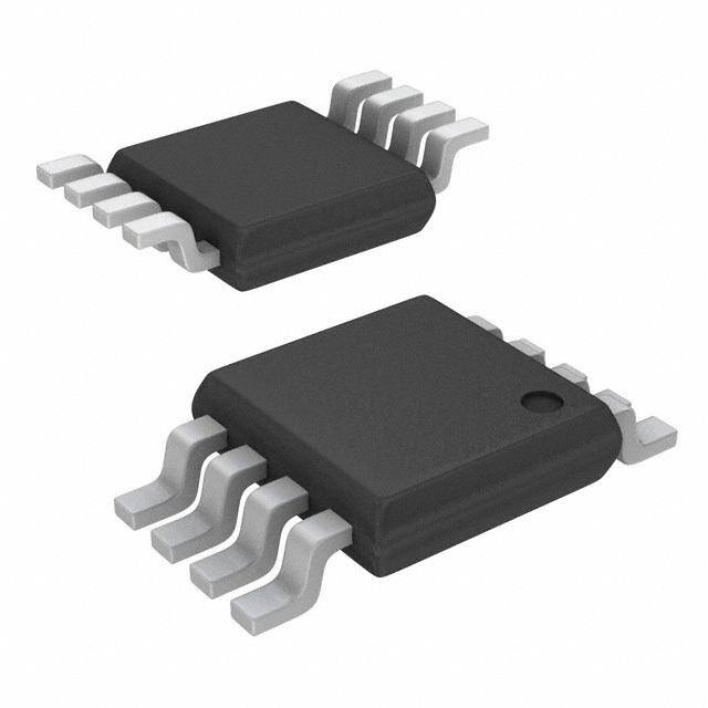
| 产品图片 |
|
| rohs | 符合RoHS无铅 / 符合限制有害物质指令(RoHS)规范要求 |
| 产品系列 | 放大器 IC,运算放大器 - 运放,STMicroelectronics LMV358LIST- |
| 数据手册 | |
| 产品型号 | LMV358LIST |
| 产品种类 | 运算放大器 - 运放 |
| 供应商器件封装 | 8-MiniSO |
| 共模抑制比—最小值 | 55 dB |
| 关闭 | No Shutdown |
| 其它名称 | 497-13055-6 |
| 其它有关文件 | http://www.st.com/web/catalog/sense_power/FM123/SC61/SS1613/LN1588/PF253625?referrer=70071840 |
| 包装 | Digi-Reel® |
| 压摆率 | 0.7 V/µs |
| 商标 | STMicroelectronics |
| 增益带宽生成 | 1 MHz |
| 增益带宽积 | 1.3MHz |
| 安装类型 | 表面贴装 |
| 安装风格 | SMD/SMT |
| 封装 | Reel |
| 封装/外壳 | 8-TSSOP,8-MSOP(0.118",3.00mm 宽) |
| 封装/箱体 | MiniSO8 |
| 工作温度 | -40°C ~ 125°C |
| 工作电源电压 | 2.7 V to 6 V |
| 工厂包装数量 | 4000 |
| 放大器类型 | 通用 |
| 最大工作温度 | + 125 C |
| 最小工作温度 | - 40 C |
| 标准包装 | 1 |
| 电压-电源,单/双 (±) | 2.7 V ~ 5.5 V |
| 电压-输入失调 | 1mV |
| 电流-电源 | 130µA |
| 电流-输入偏置 | 27nA |
| 电流-输出/通道 | 70mA |
| 电源电流 | 0.22 mA |
| 电路数 | 2 |
| 系列 | LMV358L |
| 转换速度 | 0.35 V/us |
| 输入偏压电流—最大 | 50 nA |
| 输入补偿电压 | 3 mV |
| 输出电流 | 46 mA |
| 输出类型 | 满摆幅 |
| 通道数量 | 2 Channel |


- 商务部:美国ITC正式对集成电路等产品启动337调查
- 曝三星4nm工艺存在良率问题 高通将骁龙8 Gen1或转产台积电
- 太阳诱电将投资9.5亿元在常州建新厂生产MLCC 预计2023年完工
- 英特尔发布欧洲新工厂建设计划 深化IDM 2.0 战略
- 台积电先进制程称霸业界 有大客户加持明年业绩稳了
- 达到5530亿美元!SIA预计今年全球半导体销售额将创下新高
- 英特尔拟将自动驾驶子公司Mobileye上市 估值或超500亿美元
- 三星加码芯片和SET,合并消费电子和移动部门,撤换高东真等 CEO
- 三星电子宣布重大人事变动 还合并消费电子和移动部门
- 海关总署:前11个月进口集成电路产品价值2.52万亿元 增长14.8%


PDF Datasheet 数据手册内容提取
LMV321L, LMV358L, LMV324L Low-power, general-purpose operational amplifiers Datasheet - production data Applications • Battery-powered applications • Portable devices SC70-5 SOT23-5 • Signal conditioning • Active filtering • Medical instrumentation Description MiniSO8 SO8 The LMV321L, LMV358L, and LMV324L are single, dual, and quad operational amplifiers with rail-to-rail output capabilities. They are specifically designed to operate at low voltages (2.7 V to 5 V) with enhanced performances compared to the industry standard LM3xx series. The LMV321L, LMV358L, and LMV324L are TSSOP8 offered in tiny packages, allowing the devices to be used in small portable electronic applications and to be placed closer to the actual signal. The LMV321L, LMV358L, and LMV324L are complete cost-effective solutions for application designs where cost is of primary importance. TSSOP14 SO14 Features • Low-power consumption: 250 µA max at 5 V • Low offset voltage: 7 mV max at 25 °C • Industrial temperature range: -40 °C to +125 °C • Low supply voltage: 2.7 V - 5.5 V • Gain bandwidth product: 1.3 MHz • Tiny packages December 2014 DocID023066 Rev 3 1/21 This is information on a product in full production. www.st.com
Contents LMV321L, LMV358L, LMV324L Contents 1 Package pin connections . . . . . . . . . . . . . . . . . . . . . . . . . . . . . . . . . . . . . 3 2 Absolute maximum ratings and operating conditions . . . . . . . . . . . . . 4 3 Electrical characteristics . . . . . . . . . . . . . . . . . . . . . . . . . . . . . . . . . . . . . 5 4 Application information . . . . . . . . . . . . . . . . . . . . . . . . . . . . . . . . . . . . . 11 4.1 Operating voltages . . . . . . . . . . . . . . . . . . . . . . . . . . . . . . . . . . . . . . . . . . .11 4.2 Input common-mode range . . . . . . . . . . . . . . . . . . . . . . . . . . . . . . . . . . . .11 4.3 Rail-to-rail output . . . . . . . . . . . . . . . . . . . . . . . . . . . . . . . . . . . . . . . . . . . .11 4.4 Input offset voltage drift over temperature . . . . . . . . . . . . . . . . . . . . . . . . .11 4.5 PCB layouts . . . . . . . . . . . . . . . . . . . . . . . . . . . . . . . . . . . . . . . . . . . . . . . .11 4.6 Macromodel . . . . . . . . . . . . . . . . . . . . . . . . . . . . . . . . . . . . . . . . . . . . . . . .11 5 Package information . . . . . . . . . . . . . . . . . . . . . . . . . . . . . . . . . . . . . . . . 12 5.1 SC70-5 (SOT323-5) package information . . . . . . . . . . . . . . . . . . . . . . . . 13 5.2 SOT23-5 package information . . . . . . . . . . . . . . . . . . . . . . . . . . . . . . . . . 14 5.3 MiniSO8 package information . . . . . . . . . . . . . . . . . . . . . . . . . . . . . . . . . 15 5.4 SO8 package information . . . . . . . . . . . . . . . . . . . . . . . . . . . . . . . . . . . . . 16 5.5 TSSOP8 package information . . . . . . . . . . . . . . . . . . . . . . . . . . . . . . . . . 17 5.6 TSSOP14 package information . . . . . . . . . . . . . . . . . . . . . . . . . . . . . . . . 18 5.7 SO14 package information . . . . . . . . . . . . . . . . . . . . . . . . . . . . . . . . . . . . 19 6 Ordering information . . . . . . . . . . . . . . . . . . . . . . . . . . . . . . . . . . . . . . . 20 7 Revision history . . . . . . . . . . . . . . . . . . . . . . . . . . . . . . . . . . . . . . . . . . . 20 2/21 DocID023066 Rev 3
LMV321L, LMV358L, LMV324L Package pin connections 1 Package pin connections Figure 1. Pin connections for each package (top view) Out1 1 8 Vcc+ In+ 1 5 Vcc+ In1- 2 7 Out2 Vcc- 2 In1+ 3 6 In2- In- 3 4 Out Vcc- 4 5 In2+ SC70-5/SOT23-5 MiniSO8/SO8/TSSOP8 Out1 1 14 Out4 In1- 2 13 In4- In1+ 3 12 In4+ Vcc+ 4 11 Vcc- In2+ 5 10 In3+ In2- 6 9 In3- Out2 7 8 Out3 TSSOP14/SO14 DocID023066 Rev 3 3/21 21
Absolute maximum ratings and operating conditions LMV321L, LMV358L, LMV324L 2 Absolute maximum ratings and operating conditions Table 1. Absolute maximum ratings (AMR) Symbol Parameter Value Unit V Supply voltage(1) 6 CC V Differential input voltage(2) ±V V id CC V Input pins (IN+ and IN- pins) voltage(3) V - 0.3 to V + 0.2 in CC- CC+ I Input current(4) 10 mA in T Storage temperature -65 to +150 °C stg Thermal resistance junction to ambient(5)(6) SC70-5 205 SOT23-5 250 MiniSO8 190 R °C/W thja SO8 125 TSSOP8 120 TSSOP14 100 SO14 105 T Maximum junction temperature 150 °C j HBM: human body model(7) 4000 ESD MM: machine model(8) 250 V CDM: charged device model(9) 1300 Latch-up immunity 200 mA 1. All voltage values, except differential voltage, are with respect to network ground terminal 2. Differential voltage is the non-inverting input terminal with respect to the inverting input terminal 3. VCC-Vin must not exceed 6 V, Vin must not exceed 6 V 4. Input current must be limited by a resistor in series with the inputs 5. Short-circuits can cause excessive heating and destructive dissipation 6. R are typical values th 7. Human body model: 100 pF discharged through a 1.5 kΩ resistor between two pins of the device, done for all couples of pin combinations with other pins floating. 8. Machine model: a 200 pF cap is charged to the specified voltage, then discharged directly between two pins of the device with no external series resistor (internal resistor < 5 Ω), done for all couples of pin combinations with other pins floating. 9. Charged device model: all pins plus package are charged together to the specified voltage and then discharged directly to the ground. Table 2. Operating conditions Symbol Parameter Value Unit V Supply voltage 2.7 to 5.5 CC V V Common mode input voltage range (V )- 0.2 to (V ) - 1 icm CC- CC+ T Operating free-air temperature range -40 to +125 °C oper 4/21 DocID023066 Rev 3
LMV321L, LMV358L, LMV324L Electrical characteristics 3 Electrical characteristics Table 3. Ele c trical characteristics at V = 2.7 V with V = 0 V, V = V /2, T = 25 °C, and CC+ CC- icm CC amb R connected to V /2 (unless otherwise specified) L CC Symbol Parameter Conditions Min. Typ. Max. Unit DC performance V Input offset voltage 1 7 mV io ΔV /ΔT Input offset voltage drift(1) -40 °C < T< 125 °C 5 μV/°C io I Input offset current 0.5 30 io V = V /2 nA out cc I Input bias current 27 60 ib CMRR Common mode rejection ratio(1) Vic = 0 V to Vcc-1 V, Vout = Vcc/2 70 75 dB R = 10 kΩ, high level 2.6 2.69 V L V Output swing O R = 10 kΩ, low level 65 180 mV L I Supply current (per channel) No load, V = V /2 120 180 µA CC out CC AC performance GBP Gain bandwidth product 1.3 MHz Φ Phase margin R > 1 MΩ, C = 200 pF 60 degrees m L L G Gain margin 10 dB m R > 1 MΩ, C = 200 pF SR Slew rate L L 0.6 V/μs V = 0.5 V to V - 0.5V out CC f = 1 kHz 31 nV e Equivalent input noise voltage ------------ n f = 10 kHz 20 Hz pA i Equivalent input noise current f = 1 kHz 0.30 ------------ n Hz 1. CMRR (dB) = 20 log (ΔV /ΔV ) icm io DocID023066 Rev 3 5/21 21
Electrical characteristics LMV321L, LMV358L, LMV324L Table 4. El e ctrical characteristics at V = 5 V with V = 0 V, V = V /2, T = 25 °C, and CC+ CC- icm CC amb R connected to V /2 (unless otherwise specified) L CC Symbol Parameter Conditions Min. Typ. Max. Unit DC performance 1 7 V Input offset voltage mV io -40 °C < T< 125 °C 9 ΔV /ΔT Input offset voltage drift(1) -40 °C < T< 125 °C 5 μV/°C io V = V /2 0.5 30 out cc I Input offset current io -40 °C < T< 125 °C 50 nA V = V /2 27 60 out cc I Input bias current ib -40 °C < T< 125 °C 110 CMRR Common mode rejection ratio(2) Vic = 0 V to Vcc-1 V,Vout = Vcc/2 72 75 SVRR Supply voltage rejection ratio V = 2.7 to 5 V 72 79 cc R = 2 kΩ, dB L 90 100 Avd Large signal voltage gain Vout = 0.5 V to (VCC-0.5 V) -40 °C < T< 125 °C 80 R = 10 kΩ 4.90 4.99 L R = 10 kΩ, -40 °C < T< 125 °C 4.80 L V Output swing high level V OH R = 2 kΩ 4.70 4.96 L R = 2 kΩ, -40 °C < T< 125 °C 4.60 L R = 10 kΩ 65 180 L R = 10 kΩ, -40 °C < T< 125 °C 280 L V Output swing low level mV OL R = 2 kΩ 120 300 L R = 2 kΩ, -40 °C < T< 125 °C 400 L Sinking, V = V 35 43 out CC I Output short circuit current mA out Sourcing, V = 0 V 60 70 out No load, V = V /2 130 250 out CC I Supply current (per channel) µA CC -40 °C < T< 125 °C 350 AC performance GBP Gain bandwidth product 1.3 MHz F Unity gain frequency 1 u R > 1 MΩ, C = 200 pF Φ Phase margin L L 60 degrees m G Gain margin 10 dB m R > 1 MΩ, C = 200 pF SR Slew rate L L 0.7 V/μs V = 0.5 V to V - 0.5V out CC 6/21 DocID023066 Rev 3
LMV321L, LMV358L, LMV324L Electrical characteristics Table 4. Electrical characteristics at V = 5 V with V = 0 V, V = V /2, T = 25 °C, and CC+ CC- icm CC amb R connected to V /2 (unless otherwise specified) (continued) L CC Symbol Parameter Conditions Min. Typ. Max. Unit f = 1 kHz 30 nV e Equivalent input noise voltage ------------ n f = 10 kHz 20 Hz pA i Equivalent input noise current f = 1 kHz 0.30 ------------ n Hz 1. See Section 4.4: Input offset voltage drift over temperature 2. CMRR (dB) = 20 log (ΔV /ΔV ) icm io DocID023066 Rev 3 7/21 21
Electrical characteristics LMV321L, LMV358L, LMV324L Figure 2. Supply current vs. supply voltage at Figure 3. Input offset voltage vs. input common V = V /2 mode voltage at V = 5 V icm CC CC 0.20 1.0 T=85°C T=25°C 0.9 Supply Current (mA)000...011505 T=-40°C put Offset Voltage (mV)000000......345678 T=125°C T=25°C T=-40°C n0.2 I Vicm=Vcc/2 0.1 Vcc=5V 0.00 0.0 0.0 0.5 1.0 1.5 2.0 2.5 3.0 3.5 4.0 3.0 3.5 4.0 4.5 5.0 5.5 Input Common Mode Voltage (V) Supply Voltage (V) Figure 4. Output current vs. output voltage at Figure 5. Output current vs. output voltage at V = 2.7 V V = 5 V CC CC 30 110000 Sink Sink Vid=-1V 75 Vid=-1V T=25°C T=-40°C 2200 5500 mA) 10 T=125°C T=25°C T=-40°C mA) 25 nt ( nt ( urre 00 Vcc=2.7V urre 00 T=125°C Vcc=5V C C utput -10 T=125°C T=25°C T=-40°C utput -25 T=125°C T=25°C O O --5500 --2200 -75 Source Source T=-40°C Vid=1V Vid=1V -30 --110000 00..00 0.5 11..00 1.5 22..00 2.5 00..00 0.5 11..00 1.5 22..00 2.5 33..00 3.5 44..00 4.5 55..00 Output Voltage (V) Output Voltage (V) Figure 6. Output current vs. supply voltage at Figure 7. Voltage gain and phase with V = V /2 Cl = 200 pF icm CC 110000 Sink 40 0 75 Vid=-1V T=-40°C Gain T=25°C 30 -45 5500 T=85°C T=25°C mA) 25 20 -90 put Current ( -2500 Vicm=Vcc/2 Gain (dB) 100 VccT==5-V40°C Phase --118305 Phase (°) Out ---755500 STo=u8rc5e°C T=25°C -10 VRCGillac==im25n00==k0-21Ωp.05F0V T=125°C -225 Vid=1V T=-40°C -20 -270 --110000 10k 100k 1M 10M 2.8 33..00 3.3 33..55 3.8 44..00 4.3 44..55 4.8 55..00 5.3 55..55 Frequency (Hz) Supply Voltage (V) 8/21 DocID023066 Rev 3
LMV321L, LMV358L, LMV324L Electrical characteristics Figure 8. Gain margin vs. load capacitor at Figure 9. Phase margin vs. load capacitor at V = 5 V V = 5 V CC CC 2200 90 18 Rl=600Ω T=25°C 8800 VVciccm==5V2.5V 1155 70 Rl=600Ω Vload=2.5V Gain Margin (dB) 1110038 Rl=100TkΩ=125°C Phase Margin (°) 344566000000 Rl=100Tk=Ω-40°C 55 2200 Vcc=5V T=-40°C 3 Vicm=2.5V 10 T=25°C Vload=2.5V T=125°C 00 00 100 1000 100 1000 Load Capacitor (pF) Load Capacitor (pF) Figure 10. Closed-loop gain in voltage follower Figure 11. Phase margin vs. output current at configuration for different capacitive loads V = 5 V CC 15 80 Vcc=5V Cl=500pF Sink Source Vicm=2.5V 70 1100 Rl=10kΩ T=25°C Cl=200pF 60 Cl=100pF 5 Cl=1000pF n (°)50 Cl=200pF dB) 00 argi40 Gain ( -5 hase M30 Vcc=5V Cl=100pF P20 Vicm=2.5V Vload=2.5V --1100 Cl=45pF 10 Rl=10KΩ T=25°C -15 0-1.0 -0.8 -0.6 -0.4 -0.2 0.0 0.2 0.4 0.6 0.8 1.0 1k 10k 100k 1M 10M Frequency (Hz) Output Current (mA) Figure 12. Positive and negative slew rate vs. Figure 13. Positive slew rate at V = 5 V with CC supply voltage Cl = 100 pF 0.8 22..00 1.5 00..55 11..00 T=-40°C Slew rate (V/µs) -0000....3003 T=T1=2152°5C°C TT=2=52°5C°C T=-40°C CRVVlilloc==ma12d0k==Ω0VVpcFccc/2/2 utput Voltage (V) -0000....5005 T=25°CT=125°C O --11..00 --00..55 T=-40°C Vcc=5V Vicm=Vcc/2 -1.5 Cl=100pF -0.8 Rl=1MΩ --22..00 33..00 3.5 44..00 4.5 55..00 5.5 -1 0 1 2 3 4 5 6 7 8 9 Supply Voltage (V) Time (µs) DocID023066 Rev 3 9/21 21
Electrical characteristics LMV321L, LMV358L, LMV324L Figure 14. Negative slew rate at V = 5 V with Figure 15. Noise vs. frequency CC Cl = 100 pF 22..00 Hz) 140 V Vcc=5V V/ Vicm=Vcc/2 1.5 Vicm=Vcc/2 y (n 112200 T=25°C Output Voltage (V) ---11000011........00500500 T=-40°C T=25°C T=125CR°llC==110M0ΩpF put Noise Voltage Densit 1044688000000 Vcc=5V Vcc=2.7V n -1.5 ent I 20 val --22..00 qui 00 -1 0 1 2 3 4 5 6 7 8 9 E 100 1000 10000 Time (µs) Frequency (Hz) Figure 16. Distortion + noise vs. frequency Figure 17. Distortion + noise vs. output voltage 10-1 10-1 Vcc=5V BW=80kHz Vin=1Vpp Gain=1 Rl=2kΩ Vicm=Vcc/2 Rl=2kΩ 10-2 T=25°C %) %) N ( 10-2 N ( + + HD Rl=10kΩ HD T T 10-3 Vcc=5V Gain=1 BW=22kHz Rl=10kΩ Vicm=Vcc/2 T=25°C 10-3 10-4 100 1000 10000 0.01 0.1 1 10 Frequency (Hz) Output Voltage (Vpp) 10/21 DocID023066 Rev 3
LMV321L, LMV358L, LMV324L Application information 4 Application information 4.1 Operating voltages The LMV321L, LMV358L, and LMV324L can operate from 2.7 to 5.5 V. The devices’ parameters are fully specified for 2.7 V and 5 V power supplies. Additionally, the main specifications are guaranteed in extended temperature ranges from -40 °C to 125 °C. 4.2 Input common-mode range The LMV321L, LMV358L, and LMV324L have an input common-mode range that includes ground. The input common-mode range is extended from (VCC-) - 0.2 V to (VCC+) - 1 V, with no output phase reversal. 4.3 Rail-to-rail output The operational amplifiers’ output levels can go close to the rails: 180 mV maximum above and below the rail when connected to a 10 kΩ resistive load to V /2. CC 4.4 Input offset voltage drift over temperature The maximum input voltage drift over the temperature variation is defined as follows. ΔVio Vio(T)–Vio(25°C) ---Δ----T------ = max ---------------T-----–-----2---5----°---C------------------ for Tmin < T < Tmax. 4.5 PCB layouts For correct operation, it is advised to add 10 nF decoupling capacitors as close as possible to the power supply pins. 4.6 Macromodel Accurate macromodels of the LMV321L, LMV358L, and LMV324L are available on STMicroelectronics’ web site at www.st.com. These models are a trade-off between accuracy and complexity (that is, time simulation) of the LMV321L, LMV358L, and LMV324L operational amplifiers. They emulate the nominal performances of a typical device within the specified operating conditions mentioned in the datasheet. They also help to validate a design approach and to select the right operational amplifier, but they do not replace on- board measurements. DocID023066 Rev 3 11/21 21
Package information LMV321L, LMV358L, LMV324L 5 Package information In order to meet environmental requirements, ST offers these devices in different grades of ECOPACK® packages, depending on their level of environmental compliance. ECOPACK® specifications, grade definitions and product status are available at: www.st.com. ECOPACK® is an ST trademark. 12/21 DocID023066 Rev 3
LMV321L, LMV358L, LMV324L Package information 5.1 SC70-5 (SOT323-5) package information Figure 18. SC70-5 (SOT323-5) package mechanical drawing SIDE VIEW DIMENSIONS IN MM GAUGE PLANE COPLANAR LEADS SEATING PLANE TOP VIEW Table 5. SC70-5 (or SOT323-5) package mechanical data Dimensions Ref Millimeters Inches Min Typ Max Min Typ Max A 0.80 1.10 0.315 0.043 A1 0.10 0.004 A2 0.80 0.90 1.00 0.315 0.035 0.039 b 0.15 0.30 0.006 0.012 c 0.10 0.22 0.004 0.009 D 1.80 2.00 2.20 0.071 0.079 0.087 E 1.80 2.10 2.40 0.071 0.083 0.094 E1 1.15 1.25 1.35 0.045 0.049 0.053 e 0.65 0.025 e1 1.30 0.051 L 0.26 0.36 0.46 0.010 0.014 0.018 < 0 ° 8 ° 0 ° 8 ° DocID023066 Rev 3 13/21 21
Package information LMV321L, LMV358L, LMV324L 5.2 SOT23-5 package information Figure 19. SOT23-5 package mechanical drawing GAMS1812131437CB Table 6. SOT23-5 package mechanical data Dimensions Ref. Millimeters Inches Min. Typ. Max. Min. Typ. Max. A 0.90 1.20 1.45 0.035 0.047 0.057 A1 0.15 0.006 A2 0.90 1.05 1.30 0.035 0.041 0.051 B 0.35 0.40 0.50 0.014 0.016 0.020 C 0.09 0.15 0.20 0.004 0.006 0.008 D 2.80 2.90 3.00 0.110 0.114 0.118 D1 1.90 0.075 e 0.95 0.037 E 2.60 2.80 3.00 0.102 0.110 0.118 F 1.50 1.60 1.75 0.059 0.063 0.069 L 0.10 0.35 0.60 0.004 0.014 0.024 K 0 ° 10 ° 0 ° 10 ° 14/21 DocID023066 Rev 3
LMV321L, LMV358L, LMV324L Package information 5.3 MiniSO8 package information Figure 20. MiniSO8 package mechanical drawing Table 7. MiniSO8 package mechanical data Dimensions Ref. Millimeters Inches Min. Typ. Max. Min. Typ. Max. A 1.1 0.043 A1 0 0.15 0 0.006 A2 0.75 0.85 0.95 0.030 0.033 0.037 b 0.22 0.40 0.009 0.016 c 0.08 0.23 0.003 0.009 D 2.80 3.00 3.20 0.11 0.118 0.126 E 4.65 4.90 5.15 0.183 0.193 0.203 E1 2.80 3.00 3.10 0.11 0.118 0.122 e 0.65 0.026 L 0.40 0.60 0.80 0.016 0.024 0.031 L1 0.95 0.037 L2 0.25 0.010 k 0 ° 8 ° 0 ° 8 ° ccc 0.10 0.004 DocID023066 Rev 3 15/21 21
Package information LMV321L, LMV358L, LMV324L 5.4 SO8 package information Figure 21. SO8 package mechanical drawing Table 8. SO8 package mechanical data Dimensions Ref. Millimeters Inches Min. Typ. Max. Min. Typ. Max. A 1.75 0.069 A1 0.10 0.25 0.004 0.010 A2 1.25 0.049 b 0.28 0.48 0.011 0.019 c 0.17 0.23 0.007 0.010 D 4.80 4.90 5.00 0.189 0.193 0.197 E 5.80 6.00 6.20 0.228 0.236 0.244 E1 3.80 3.90 4.00 0.150 0.154 0.157 e 1.27 0.050 h 0.25 0.50 0.010 0.020 L 0.40 1.27 0.016 0.050 L1 1.04 0.040 k 0 ° 8 ° 1 ° 8 ° ccc 0.10 0.004 16/21 DocID023066 Rev 3
LMV321L, LMV358L, LMV324L Package information 5.5 TSSOP8 package information Figure 22. TSSOP8 package mechanical drawing Table 9. TSSOP8 package mechanical data Dimensions Ref. Millimeters Inches Min. Typ. Max. Min. Typ. Max. A 1.2 0.047 A1 0.05 0.15 0.002 0.006 A2 0.80 1.00 1.05 0.031 0.039 0.041 b 0.19 0.30 0.007 0.012 c 0.09 0.20 0.004 0.008 D 2.90 3.00 3.10 0.114 0.118 0.122 E 6.20 6.40 6.60 0.244 0.252 0.260 E1 4.30 4.40 4.50 0.169 0.173 0.177 e 0.65 0.0256 k 0° 8° 0° 8° L 0.45 0.60 0.75 0.018 0.024 0.030 L1 1 0.039 aaa 0.1 0.004 DocID023066 Rev 3 17/21 21
Package information LMV321L, LMV358L, LMV324L 5.6 TSSOP14 package information Figure 23. TSSOP14 package mechanical drawing Table 10. TSSOP14 package mechanical data Dimensions Ref. Millimeters Inches Min. Typ. Max. Min. Typ. Max. A 1.20 0.047 A1 0.05 0.15 0.002 0.004 0.006 A2 0.80 1.00 1.05 0.031 0.039 0.041 b 0.19 0.30 0.007 0.012 c 0.09 0.20 0.004 0.0089 D 4.90 5.00 5.10 0.193 0.197 0.201 E 6.20 6.40 6.60 0.244 0.252 0.260 E1 4.30 4.40 4.50 0.169 0.173 0.176 e 0.65 0.0256 L 0.45 0.60 0.75 0.018 0.024 0.030 L1 1.00 0.039 k 0 ° 8 ° 0 ° 8 ° aaa 0.10 0.004 18/21 DocID023066 Rev 3
LMV321L, LMV358L, LMV324L Package information 5.7 SO14 package information Figure 24. SO14 package mechanical drawing Table 11. SO14 package mechanical data Dimensions Millimeters Inches Ref. Min. Typ. Max. Min. Typ. Max. A 1.35 1.75 0.05 0.068 A1 0.10 0.25 0.004 0.009 A2 1.10 1.65 0.04 0.06 B 0.33 0.51 0.01 0.02 C 0.19 0.25 0.007 0.009 D 8.55 8.75 0.33 0.34 E 3.80 4.0 0.15 0.15 e 1.27 0.05 H 5.80 6.20 0.22 0.24 h 0.25 0.50 0.009 0.02 L 0.40 1.27 0.015 0.05 k 8 ° (max.) ddd 0.10 0.004 DocID023066 Rev 3 19/21 21
Ordering information LMV321L, LMV358L, LMV324L 6 Ordering information Table 12. Order codes for devices without shutdown feature Order code Temperature range Package Packing Marking LMV321LICT SC70-5 K25 LMV321LILT SOT23-5 K170 LMV358LIST MiniSO8 K170 LMV358LIPT -40 °C to +125 °C TSSOP8 Tape and reel V358L LMV358LIDT SO8 LMV358L LMV324LIPT TSSOP14 LMV324L LMV324LIDT SO14 LMV324L 7 Revision history Table 13. Document revision history Date Revision Changes 04-May-2012 1 Initial release. 19-Dec-2013 2 New template Added TSSOP8 package 09-Dec-2014 3 Table 6: updated some of the “inches” dimensions Table 12: added new order code LMV358LIPT 20/21 DocID023066 Rev 3
LMV321L, LMV358L, LMV324L IMPORTANT NOTICE – PLEASE READ CAREFULLY STMicroelectronics NV and its subsidiaries (“ST”) reserve the right to make changes, corrections, enhancements, modifications, and improvements to ST products and/or to this document at any time without notice. Purchasers should obtain the latest relevant information on ST products before placing orders. ST products are sold pursuant to ST’s terms and conditions of sale in place at the time of order acknowledgement. Purchasers are solely responsible for the choice, selection, and use of ST products and ST assumes no liability for application assistance or the design of Purchasers’ products. No license, express or implied, to any intellectual property right is granted by ST herein. Resale of ST products with provisions different from the information set forth herein shall void any warranty granted by ST for such product. ST and the ST logo are trademarks of ST. All other product or service names are the property of their respective owners. Information in this document supersedes and replaces information previously supplied in any prior versions of this document. © 2014 STMicroelectronics – All rights reserved DocID023066 Rev 3 21/21 21
Mouser Electronics Authorized Distributor Click to View Pricing, Inventory, Delivery & Lifecycle Information: S TMicroelectronics: LMV324LIDT LMV324LIPT LMV321LICT LMV321LILT LMV358LIST LMV358LIDT LMV358LIPT