ICGOO在线商城 > 集成电路(IC) > 线性 - 放大器 - 仪表,运算放大器,缓冲器放大器 > OP497GPZ
 Datasheet下载
- 型号: OP497GPZ
- 制造商: Analog
- 库位|库存: xxxx|xxxx
- 要求:
| 数量阶梯 | 香港交货 | 国内含税 |
| +xxxx | $xxxx | ¥xxxx |
查看当月历史价格
查看今年历史价格
OP497GPZ产品简介:
ICGOO电子元器件商城为您提供OP497GPZ由Analog设计生产,在icgoo商城现货销售,并且可以通过原厂、代理商等渠道进行代购。 OP497GPZ价格参考。AnalogOP497GPZ封装/规格:线性 - 放大器 - 仪表,运算放大器,缓冲器放大器, 通用 放大器 4 电路 14-PDIP。您可以下载OP497GPZ参考资料、Datasheet数据手册功能说明书,资料中有OP497GPZ 详细功能的应用电路图电压和使用方法及教程。
OP497GPZ 是由 Analog Devices Inc. 生产的一款四通道低噪声、高精度运算放大器,属于线性 - 放大器 - 仪表、运算放大器、缓冲器放大器类别。其典型应用场景包括以下几类:

1. 精密测量与信号调理
   OP497GPZ 的低失调电压(最大 55 µV)和低温漂特性(最大 3 µV/°C),使其非常适合用于需要高精度的信号调理电路中,例如工业传感器信号放大、医疗设备中的生物电信号采集(如心电图 ECG 或脑电图 EEG)、以及环境监测系统中的温度或压力传感器信号处理。

2. 数据采集系统 (DAQ)
   在多通道数据采集系统中,OP497GPZ 可以用作前置放大器或缓冲器,将微弱的模拟信号放大到适合 ADC 转换的范围。它支持宽电源电压范围(±15 V 单位增益稳定),能够适应多种输入信号电平需求。

3. 音频应用
   由于其低噪声性能(1 kHz 下为 8 nV/√Hz),该器件也可应用于高品质音频设备中,比如麦克风前置放大器或耳机驱动电路,提供清晰且失真小的声音输出。

4. 自动化控制与过程监控
   在工业自动化领域,OP497GPZ 常被用作反馈放大器,在 PID 控制器或其他闭环控制系统中实现精确的速度、位置或流量控制。此外,它还能处理来自各种现场设备(如变送器)的低电平电流或电压信号。

5. 科学仪器
   对于需要极高稳定性和准确性的实验装置,如光谱仪、色谱仪等,OP497GPZ 的高性能参数确保了对微弱光学或化学信号的有效捕捉和放大。

总之,OP497GPZ 凭借其出色的电气特性和可靠性,广泛适用于要求高精度、低噪声及多通道处理能力的各种电子系统中。
| 参数 | 数值 |
| -3db带宽 | - |
| 产品目录 | 集成电路 (IC)半导体 |
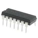
| 描述 | IC OPAMP GP 500KHZ 14DIP精密放大器 QUAD PREC INPUT CRNT 75uV Max |
| 产品分类 | Linear - Amplifiers - Instrumentation, OP Amps, Buffer Amps集成电路 - IC |
| 品牌 | Analog Devices |
| 产品手册 | |
| 产品图片 |
|
| rohs | 符合RoHS无铅 / 符合限制有害物质指令(RoHS)规范要求 |
| 产品系列 | 放大器 IC,精密放大器,Analog Devices OP497GPZ- |
| 数据手册 | |
| 产品型号 | OP497GPZ |
| 产品培训模块 | http://www.digikey.cn/PTM/IndividualPTM.page?site=cn&lang=zhs&ptm=30008http://www.digikey.cn/PTM/IndividualPTM.page?site=cn&lang=zhs&ptm=26202 |
| 产品目录页面 | |
| 产品种类 | 精密放大器 |
| 供应商器件封装 | 14-PDIP |
| 共模抑制比—最小值 | 135 dB |
| 关闭 | No |
| 包装 | 管件 |
| 压摆率 | 0.15 V/µs |
| 双重电源电压 | +/- 3 V, +/- 5 V, +/- 9 V, +/- 12 V, +/- 15 V, +/- 18 V |
| 商标 | Analog Devices |
| 增益带宽生成 | 500 kHz |
| 增益带宽积 | 500kHz |
| 安装类型 | 通孔 |
| 安装风格 | Through Hole |
| 封装 | Tube |
| 封装/外壳 | 14-DIP(0.300",7.62mm) |
| 封装/箱体 | PDIP-14 |
| 工作温度 | -40°C ~ 85°C |
| 工作电源电压 | 2 V to 20 V |
| 工厂包装数量 | 25 |
| 放大器类型 | 通用 |
| 最大双重电源电压 | +/- 20 V |
| 最大工作温度 | + 85 C |
| 最小双重电源电压 | +/- 2 V |
| 最小工作温度 | - 40 C |
| 标准包装 | 25 |
| 电压-电源,单/双 (±) | ±2 V ~ 20 V |
| 电压-输入失调 | 80µV |
| 电压增益dB | 132.04 dB |
| 电流-电源 | 525µA |
| 电流-输入偏置 | 60pA |
| 电流-输出/通道 | 25mA |
| 电源电压-最大 | 20 V |
| 电源电压-最小 | 2 V |
| 电源电流 | 525 uA |
| 电源类型 | Dual |
| 电路数 | 4 |
| 系列 | OP497 |
| 视频文件 | http://www.digikey.cn/classic/video.aspx?PlayerID=1364138032001&width=640&height=505&videoID=2245193153001http://www.digikey.cn/classic/video.aspx?PlayerID=1364138032001&width=640&height=505&videoID=2245193159001 |
| 转换速度 | 0.15 V/us |
| 输入偏压电流—最大 | 200 pA |
| 输入电压范围—最大 | 14 V |
| 输入补偿电压 | 80 uV |
| 输出电流 | 25 mA |
| 输出类型 | No |
| 通道数量 | 4 Channel |


PDF Datasheet 数据手册内容提取
Precision Picoampere Input Current Quad Operational Amplifier OP497 FEATURES PIN CONNECTIONS Low offset voltage: 75 μV maximum OUT A 1 16 OUT D Low offset voltage drift: 1.0 μV/°C maximum –IN A 2 15 –IN D Very low bias current +IN A 3 14 +IN D 25°C: 150 pA maximum V+ 4 OP497 13 V– −40°C to +85°C: 300 pA maximum +IN B 5 12 +IN C Very high open-loop gain: 2000 V/mV minimum –IN B 6 11 –IN C Low supply current (per amplifier): 625 μA maximum OUT B 7 10 OUT C OHipgehr actoems mfroomn- m±2o Vd et ore ±j2ec0t Vio snu: p1p1l4ie dsB minimum NC 8NC = NO CONNECT9 NC 00309-001 Figure 1. 16-Lead Wide Body SOIC (RW-16) APPLICATIONS OUT A 1 14 OUT D Strain gage and bridge amplifiers –IN A 2 13 –IN D High stability thermocouple amplifiers +IN A 3 12 +IN D Instrumentation amplifiers V+ 4 OP497 11 V– Photocurrent monitors +IN B 5 10 +IN C High gain linearity amplifiers –IN B 6 9 –IN C LSoamngp-ltee-ramn din-hteogldra atmorps/lfifiliteerrss OUT B 7 8 OUT C 00309-002 Figure 2. 14-Lead PDIP (N-14) Peak detectors Logarithmic amplifiers 1k VS = ±15V Battery-powered systems VCM = 0V GENERAL DESCRIPTION A) p The OP497 is a quad op amp with precision performance in T ( N the space-saving, industry standard 16-lead SOlC package. RE R 100 Its combination of exceptional precision with low power and CU T extremely low input bias current makes the quad OP497 useful PU –IB N in a wide variety of applications. I Precision performance of the OP497 includes very low offset +IB (<50 μV) and low drift (<0.5 μV/°C). Open-loop gain exceeds IOS 2000 V/mV ensuring high linearity in every application. Errors 10 dmuoed teo rceojemctmioonn o-mf >o1d2e0 s digBn. aTlsh aer Oe ePl4im97i nhaatse da pbyo wites rc soumpmploy n- –75 –50 –25 TE0MPER2A5TURE 5(°0C) 75 100 125 00309-003 Figure 3. Input Bias, Offset Current vs. Temperature rejection of >120 dB which minimizes offset voltage changes Combining precision, low power, and low bias current, the OP497 experienced in battery-powered systems. The supply current is ideal for a number of applications, including instrumentation of the OP497 is <625 μA per amplifier, and it can operate with amplifiers, log amplifiers, photodiode preamplifiers, and long- supply voltages as low as ±2 V. term integrators. For a single device, see the OP97 data sheet, The OP497 uses a superbeta input stage with bias current and for a dual device, see the OP297 data sheet. cancellation to maintain picoamp bias currents at all temperatures. This is in contrast to FET input op amps whose bias currents start in the picoamp range at 25°C but double for every 10°C rise in temperature to reach the nanoamp range above 85°C. The input bias current of the OP497 is <100 pA at 25°C. Rev. E Information furnished by Analog Devices is believed to be accurate and reliable. However, no responsibility is assumed by Analog Devices for its use, nor for any infringements of patents or other One Technology Way, P.O. Box 9106, Norwood, MA 02062-9106, U.S.A. rights of third parties that may result from its use. Specifications subject to change without notice. No license is granted by implication or otherwise under any patent or patent rights of Analog Devices. Tel: 781.329.4700 www.analog.com Trademarks and registered trademarks are the property of their respective owners. Fax: 781.461.3113 ©1991–2009 Analog Devices, Inc. All rights reserved.
OP497 TABLE OF CONTENTS Features .............................................................................................. 1 AC Performance ......................................................................... 10 Applications ....................................................................................... 1 Guarding And Shielding ........................................................... 11 General Description ......................................................................... 1 Open-Loop Gain Linearity ....................................................... 11 Pin Connections ............................................................................... 1 Applications Circuit ....................................................................... 12 Revision History ............................................................................... 2 Precision Absolute Value Amplifier ......................................... 12 Specifications ..................................................................................... 3 Precision Current Pump ............................................................ 12 Absolute Maximum Ratings ............................................................ 4 Precision Positive Peak Detector .............................................. 12 Thermal Resistance ...................................................................... 4 Simple Bridge Conditioning Amplifier ................................... 12 ESD Caution .................................................................................. 4 Nonlinear Circuits ...................................................................... 13 Typical Performance Characteristics ............................................. 5 Outline Dimensions ....................................................................... 14 Applications Information .............................................................. 10 Ordering Guide .......................................................................... 15 REVISION HISTORY 2/09—Rev. D to Rev. E 11/01—Rev. C to Rev. D Deleted 14-Lead CERDIP ............................................. Throughout Edits to Pin Connection Headings .................................................. 1 Changes to Features Section and General Description Deleted Wafer Test Limits ................................................................ 3 Section ................................................................................................ 1 Edits to Absolute Maximum Ratings .............................................. 5 Delete Military Processed Devices Text, SMD Part Number, Edits to Outline Dimensions ......................................................... 16 ADI Part Number Table, and Dice Characteristics Figure ......... 3 Edits to Ordering Guide ................................................................ 17 Changes to Table 1 ............................................................................ 3 Changes to Absolute Maximum Ratings Section ......................... 4 Changes to Figure 12 ........................................................................ 6 Changes to Figure 18 and Figure 19 ............................................... 7 Changes to Figure 26 and Figure 28 ............................................... 8 Deleted OP497 Spice Macro-Model Section ............................... 10 Changes to Applications Information Section ............................ 10 Moved Figure 33 ............................................................................. 10 Deleted Table I. OP497 SPICE Net-List....................................... 11 Changes to Open-Loop Gain Linearity Section and Figure 35 .......................................................................................... 11 Changes to Figure 40 ...................................................................... 13 Updated Outline Dimensions ....................................................... 14 Changes to Ordering Guide .......................................................... 15 Rev. E | Page 2 of 16
OP497 SPECIFICATIONS T = 25°C, V = ±15 V, unless otherwise noted. A S Table 1. F Grade G Grade Parameter Symbol Condition Min Typ Max Min Typ Max Unit INPUT CHARACTERISTICS Offset Voltage V 40 75 80 150 μV OS −40°C ≤ +85°C 70 150 120 250 μV Average Input Offset Voltage Drift TCV T − T 0.4 1.0 0.6 1.5 μV/°C OS MIN MAX Long-Term Input Offset Voltage 0.1 0.1 μV/Month Stability Input Bias Current I V = 0 V 40 150 60 200 pA B CM −40° ≤ T ≤ +85°C 60 200 80 300 pA A Average Input Bias Current Drift TC −40° ≤ T ≤ +85°C 0.3 0.3 pA/°C IB A Input Offset Current I V = 0 V 30 150 50 200 pA OS CM −40° ≤ T ≤ +85°C 50 200 80 300 pA A Average Input Offset Current Drift T I 0.3 0.4 pA/°C COS Input Voltage Range1 IVR ±13 ±14 ±13 ±14 V T − T ±13 ±13.5 ±13 ±13.5 V MIN MAX Common-Mode Rejection CMR V = ±13 V 114 135 114 135 dB CM T − T 108 120 108 120 dB MIN MAX Large Signal Voltage Gain A V = ±10 V, R = 2 kΩ 1500 4000 1200 4000 V/mV VO O L −40° ≤ T ≤ +85°C 800 2000 800 2000 V/mV A Input Resistance Differential Mode R 30 30 MΩ IN Input Resistance Common Mode R 500 500 GΩ INCM Input Capacitance C 3 3 pF IN OUTPUT CHARACTERISTICS Output Voltage Swing V R = 2 kΩ ±13 ±13.7 ±13 ±13.7 V O L R = 10 kΩ, T − T ±13 ±14 ±13 ±14 V L MIN MAX R = 10 kΩ ±13 ±13.5 ±13 ±13.5 V L Short Circuit I ±25 ±25 mA SC POWER SUPPLY Power Supply Rejection Ratio PSRR V = ±2 V to ±20 V 114 135 114 135 dB S V = ±2.5 V to ±20 V, T − T 108 120 108 120 dB S MIN MAX Supply Current (per Amplifier) I No load 525 625 525 625 μA SY T − T 580 750 580 750 μA MIN MAX Supply Voltage Range V Operating range ±2 ±20 ±2 ±20 V S T − T ±2.5 ±20 ±2.5 ±20 V MIN MAX DYNAMIC PERFORMANCE Slew Rate SR 0.05 0.15 0.05 0.15 V/μs Gain Bandwidth Product GBW 500 500 kHz Channel Separation CS V = 20 V p-p, f = 10 Hz 150 150 dB O O NOISE PERFORMANCE Voltage Noise e p-p 0.1 Hz to 10 Hz 0.3 0.3 μV/p-p n Voltage Noise Density e e = 10 Hz 17 17 nV/√Hz n n e = 1 kHz 15 15 nV/√Hz n Current Noise Density i i = 10 Hz 20 20 fA/√Hz n n 1 Guaranteed by CMR test. Rev. E | Page 3 of 16
OP497 ABSOLUTE MAXIMUM RATINGS THERMAL RESISTANCE Absolute maximum ratings apply to packaged parts. θ is specified for the worst-case mounting conditions, that is, JA Table 2. θ is specified for a device in socket for the PDIP package, and JA Parameter Rating θ is specified for a device soldered to the printed circuit board JA Supply Voltage ±20 V (PCB) for the SOIC package. Input Voltage1 20 V Differential Input Voltage1 40 V Table 3. Output Short-Circuit Duration Indefinite Package Type θ θ Unit JA JC Storage Temperature Range −65°C to +150°C 14-Lead PDIP (N-14) 76 33 °C/W Operating Temperature Range −40°C to +85°C 16-Lead SOIC (RW-16) 92 23 °C/W Junction Temperature Range −65°C to +150°C Lead Temperature (Soldering, 60 sec) 300°C 1 For supply voltages less than ±20 V, the absolute maximum input voltage is – 1/4 equal to the supply voltage. OP497 V1 20V p-p @ 10Hz + 2kΩ 50kΩ Stresses above those listed under Absolute Maximum Ratings may cause permanent damage to the device. This is a stress 50Ω – rating only; functional operation of the device at these or any OP1/4497 V2 other conditions above those indicated in the operational + section of this specification is not implied. Exposure to absolute maximum rating conditions for extended periods may affect CHANNEL SEPARATION = 20 log(V2/1V01,000) 00309-004 device reliability. Figure 4. Channel Separation Test Circuit ESD CAUTION Rev. E | Page 4 of 16
OP497 TYPICAL PERFORMANCE CHARACTERISTICS T = 25°C, V = ±15 V, unless otherwise noted. A S 50 50 TA = 25°C VS = ±15V VS = ±15V VCM = 0V VCM = 0V 40 40 S S T T NI NI U U F 30 F 30 O O E E G G A A T T N 20 N 20 E E C C R R E E P P 10 10 0 0 –100 –80 –60 IN–4P0UT O–2F0FSET0 VOL2T0AGE 4(µ0V) 60 80 100 00309-006 0 0.1 0.2 0.3TCVOS0 .(4µV/°C0).5 0.6 0.7 0.8 00309-009 Figure 5. Typical Distribution of Input Offset Voltage Figure 8. Typical Distribution of TCVOS 50 1k TA = 25°C VS = ±15V VS = ±15V VCM = 0V VCM = 0V 40 S GE OF UNIT 30 RRENT (pA) 100 A U T C PERCEN 20 INPUT –IB 10 +IB IOS 0 10 –100 –80 –60 –I4N0PUT– 2B0IAS C0URRE20NT (p4A0) 60 80 100 00309-007 –75 –50 –25 TE0MPERA25TURE (5°0C) 75 100 125 00309-010 Figure 6. Typical Distribution of Input Bias Current Figure 9. Input Bias, Offset Current vs. Temperature 60 70 TA = 25°C TA = 25°C VS = ±15V VS = ±15V 50 VCM = 0V 60 NITS 40 T (pA) 50 –IB U N OF RE 40 GE 30 CUR +IB ENTA BIAS 30 PERC 20 NPUT 20 I 10 10 0 0 0 10 INPU20T OFFSET30 CURREN4T0 (pA) 50 60 00309-008 –15 –10 COM–5MON-MOD0E VOLTAG5E (V) 10 15 00309-011 Figure 7. Typical Distribution of Input Offset Current Figure 10. Input Bias Current vs. Common-Mode Voltage Rev. E | Page 5 of 16
OP497 ±3 1k TA = 25°C TA = 25°C VS = ±15V VS = ±2V TO ±20V FINAL VALUE (µV) ±2 VCM = 0V DENSITY (nV/Hz) 100 CURRENT NOISE DENSITY (fA/Hz) M E E RO OIS VOLTAGE NOISE OIS ON F ±1 GE N 10 NT N DEVIATI VOLTA CURRE 0 1 0 T1IME AFTER P2OWER APP3LIED (Minute4s) 5 00309-012 1 10FREQUENCY (Hz)100 1k 00309-015 Figure 11. Input Offset Voltage Warm-Up Drift Figure 14. Voltage Noise Density vs. Frequency 10k 10 BALANCED OR UNBALANCED TA = 25°C VS = ±15V VS = ±2V TO ±20V V) VCM = 0V E (µ Hz) OFFSET VOLTAG 1k SE DENSITY (µV/ 1 10Hz 1kHz VE 100 TA = 25°C NOI 0.1 TI L C A E T F O EF T 10 0.01 10 100 SO1kURCE RE1S0kISTANC1E0 0(Ωk) 1M 10M 00309-013 100 1k SOUR1C0kE RESIST1A0N0CkE (Ω) 1M 10M 00309-016 Figure 12. Effective Offset Voltage vs. Source Resistance Figure 15. Total Noise Density vs. Source Resistance 100 BALANCED OR UNBALANCED µV/°C) VVSC M= =± 105VV V) 100 5mV 1s E ( DI 90 G V/ A 10 m LT 00 O 1 ECTIVE OFFSET V 1 NOISE VOLTAGE ( 100% FF VS = ±15V E TA = 25°C 0.1 100 1k S1O0UkRCE R1E0S0IkSTANCE1 M(Ω) 10M 100M 00309-014 0 2 TI4ME (Second6s) 8 10 00309-017 Figure 13. Effective TCVOS vs. Source Resistance Figure 16. 0.1 Hz to 10 Hz Noise Voltage Rev. E | Page 6 of 16
OP497 100 160 VS = ±15V VS = ±15V CL = 30pF TA = 25°C 80 RL = 1MΩ 140 GAIN TA = 25°C dB) B) 60 ON ( 120 EN-LOOP GAIN (d 2400 PHASE 19305 PHASE (Degrees) N-MODE REJECTI 1086000 OP 0 180 MMO 40 O C –20 225 20 –40 0 100 1k F1R0EkQUENCY1 0(H0zk) 1M 10M 00309-018 1 10 100FREQUE1kNCY (Hz)10k 100k 1M 00309-021 Figure 17. Open-Loop Gain and Phase vs. Frequency Figure 20. Common-Mode Rejection vs. Frequency 10k 160 VS = ±15V TA = 25°C 140 TA = 25°C B) d V) N ( 120 V/m TA = 125°C TIO –PSR AIN ( EJEC 100 +PSR P G 1k Y R 80 O L O P N-L SUP 60 OPE WER 40 O P 20 VS = ±15V VO = ±10V 100 0 1 LOAD RESISTANCE (kΩ) 10 20 00309-019 1 10 100FREQUE1kNCY (Hz)10k 100k 1M 00309-022 Figure 18. Open-Loop Gain vs. Load Resistance Figure 21. Power Supply Rejection vs. Frequency 35 µV/DIV) RVVSCL N== =±2 1k±5Ω1V0V 30 1VTA%ASV C ==TL H2 ±=51D °5+CV1 E (10 TA = 125°C p) 25 RL = 10kΩ VOLTAG TA = 25°C NG (V p- 20 T WI U S NTIAL INP OUTPUT 1150 E R E F 5 F DI 0 –15 –10 –O5UTPUT V0OLTAGE (V5) 10 15 00309-020 100 1kFREQUENCY (Hz)10k 100k 00309-023 Figure 19. Open-Loop Gain Linearity Figure 22. Maximum Output Swing vs. Frequency Rev. E | Page 7 of 16
OP497 +VS 700 TA = 25°C NO LOAD E (V)GES) –0.5 R) (µA) 600 125°C AGTA –1.0 FIE DE VOLTPLY VOL –1.5 R AMPLI 500 25°C OP E T COMMON-MERRED TO SU 11..50 Y CURRENT (P 400 PUEF PL 300 IN(R 0.5 UP S –VS0 ±5 SUPPLY V±O10LTAGE (V) ±15 ±20 00309-024 2000 ±5 SUPPLY V±O10LTAGE (V) ±15 ±20 00309-027 Figure 23. Input Common-Mode Voltage Range vs. Supply Voltage Figure 26. Supply Current (per Amplifier) vs. Supply Voltage 35 1k VS = ±15V VS = ±15V TA = 25°C TA = 25°C 30 1A%VC TLH =D +1 100 fO = 1kHz p) 25 V p- Ω) 10 G ( 20 E ( N C WI AN 1 S D UT 15 PE AV = +1 P M T I 0.1 U O 10 0.01 5 010 1L0O0AD RESISTANCE (1Ωk) 10k 00309-025 0.0011 10 F1R0E0QUENCY (1Hkz) 10k 100k 00309-028 Figure 24. Maximum Output Swing vs. Load Resistance Figure 27. Closed-Loop Output Impedance vs. Frequency +VS 35 S) –0.5 TRAL == 2150°kCΩ 30 T VOLTAGE SWING (V)D TO SUPPLY VOLTAGE ––111...055 CIRCUIT CURRENT (mA) –11225505 VOTOSU T=G P±RU1O5TUV SNHDORTED TTAA == 12255°°CC OUTPU(REFERRE 10..05 SHORT- –––232005 TTAA == 2152°5C°C –VS0 ±5 SUPPLY V±O10LTAGE (V) ±15 ±20 00309-026 –350 TIM1E FROM OUTPU2T SHORT (Minu3tes) 4 00309-029 Figure 25. Output Voltage Swing vs. Supply Voltage Figure 28. Short-Circuit Current vs. Time at Various Temperatures Rev. E | Page 8 of 16
OP497 70 VS = ±15V TA = 25°C 60 AVCL = +1 VOUT = 100mV p-p 50 %) T ( 40 O O H S R 30 E V O 20 10 0 10 L1O0A0D CAPACITANCE 1(pkF) 10k 00309-030 Figure 29. Small-Signal Overshoot vs. Load Capacitance Rev. E | Page 9 of 16
OP497 APPLICATIONS INFORMATION Extremely low bias current makes the OP497 attractive for use in sample-and-hold amplifiers, peak detectors, and log amplifiers that must operate over a wide temperature range. Balancing 100 90 input resistances is not necessary with the OP497. High source resistance, even when unbalanced, only minimally degrades the offset voltage and TCV . OS The input pins of the OP497 are protected against large differential voltage by back-to-back diodes and current-limiting resistors. 10 Common-mode voltages at the inputs are not restricted and 0% mThaey OvaPr4y9 o7v reerq tuhier efsu lvle rrayn lgitet loef otphee rsautipnpgl yh veoadltraogoems u asbedo.u t the 20mV 5µs 00309-033 Figure 31. Small Signal Transient Response (CLOAD = 1000 pF, AVCL = +1) supply rails and is specified for operation with supplies as low as ±2 V. Typically, the common-mode range extends to within 1 V of either rail. When using a 10 kΩ load, the output typically swings to within 1 V of the rails. 100 AC PERFORMANCE 90 The ac characteristics of the OP497 are highly stable over its full operating temperature range. Figure 30 shows the unity-gain small signal response. Extremely tolerant of capacitive loading on the output, the OP497 displays excellent response even with 1000 pF loads (see Figure 31). 10 0% 2V 50µs 00309-034 100 Figure 32. Large Signal Transient Response (AVCL = +1) 90 10 0% 20mV 5µs 00309-032 Figure 30. Small Signal Transient Response (CLOAD = 100 pF, AVCL = +1) V+ VOUT 2.5kΩ –IN 2.5kΩ +IN V– 00309-031 Figure 33. Simplified Schematic Showing One Amplifier Rev. E | Page 10 of 16
OP497 GUARDING AND SHIELDING OPEN-LOOP GAIN LINEARITY To maintain the extremely high input impedances of the OP497, The OP497 has both an extremely high gain of 2000 V/mV care must be taken in circuit board layout and manufacturing. typical and constant gain linearity. This enhances the precision Board surfaces must be kept scrupulously clean and free of of the OP497 and provides for very high accuracy in high moisture. Conformal coating is recommended to provide a closed-loop gain applications. Figure 35 illustrates the typical humidity barrier. Even a clean PCB can have 100 pA of leakage open-loop gain linearity of the OP497. currents between adjacent traces; therefore, use guard rings atoro tuhnatd o tnh et hine pinuptsu. tGs,u aasr dsh torwacne si na rFei goupreer a3t4e,d s oat tah avto lletaagkea gcelo se V/DIV) RVVSCL M== =±1 1005kVVΩ µ currents become minimal. In noninverting applications, connect E (10 TA = 125°C the guard ring to the common-mode voltage at the inverting G A T input. In inverting applications, both inputs remain at ground; OL therefore, the guard trace should be grounded. Place guard T V TA = 25°C U traces on both sides of the circuit board. NP L I UNITY-GAIN FOLLOWER NONINVERTING AMPLIFIER TIA N E R E – – F F 1/4 1/4 DI OP497 OP497 + + –15 –10 –O5UTPUT VO0LTAGE (V5) 10 15 00309-036 INVERTING AMPLIFIER PDIP Figure 35. Open-Loop Gain Linearity BOTTOM VIEW 8 1 – 1/4 A OP497 + B 00309-035 Figure 34. Guard Ring Layout and Connections Rev. E | Page 11 of 16
OP497 APPLICATIONS CIRCUIT PRECISION ABSOLUTE VALUE AMPLIFIER PRECISION POSITIVE PEAK DETECTOR The circuit in Figure 36 is a precision absolute value amplifier In Figure 38, the CH must be of polystyrene, Teflon®, or with an input impedance of 30 MΩ. The high gain and low polyethylene to minimize dielectric absorption and leakage. TCVOS of the OP497 ensure accurate operation with microvolt The droop rate is determined by the size of CH and the bias current of the OP497. input signals. In this circuit, the input always appears as a common- mode signal to the op amps. The CMR of the OP497 exceeds 1kΩ 120 dB, yielding an error of less than 2 ppm. +15V 0.1µF 1N4148 +15V 2 1/4 1 6 8+ 0.C12µF 1Rk1Ω 1Rk3Ω VIN 1kΩ 3 OP497 2N930 1kΩ5 OP1/4497 7 VOUT CH + 4 0.1µF C1 D1 30pF 1N4148 6 + 2 8 1/4 7 1kΩ VIN 3 OP1/444970.C13µ1F 1ND41248 R2k2Ω5 OP497 0V < VOUT < 10V Figure 3R8E.S PErTecision Positive Peak D–e1t5eVctor 00309-039 –15V 00309-037 SFiIgMurPe L3E9 sBhRowIDs Ga sEim CpOleN bDridITgeIO coNnIdNitGio nAinMg PamLIpFliIfEieRr using Figure 36. Precision Absolute Value Amplifier the OP497. The transfer function is PRECISION CURRENT PUMP ⎛ ΔR ⎞R Maximum output current of the precision current pump shown V =V ⎜ ⎟ F OUT REF⎜R+ΔR⎟ R in Figure 37 is ±10 mA. Voltage compliance is ±10 V with ±15 V ⎝ ⎠ supplies. Output impedance of the current transmitter exceeds The REF43 provides an accurate and stable reference voltage for 3 MΩ with linearity better than 16 bits. the bridge. To maintain the highest circuit accuracy, R should F R3 be 0.1% or better with a low temperature coefficient. 10kΩ R1 +5V 10kΩ – 2 R5 2 VIN 10Rk2Ω OP1/4497 1 10kΩ ±IO1U0TmA REF43 6 2.5V VREF RF + 3 +15V R R 4 2 10Rk4Ω 7 18/4 5 R R + ΔR OP1/4497 1 VOUT OP497 3 6 IOUT =VRI5N=1V00INΩ=10mA/V 4 +5V –15V 00309-038 6OP1/44987 7 VOUT = VREF( R Δ+ RΔR ) RRF Figure 37. Precision Current Pump 5 –5V4 00309-040 Figure 39. Simple Bridge Conditioning Amplifier Using the OP497 Rev. E | Page 12 of 16
OP497 NONLINEAR CIRCUITS A similar analysis made for the square root amplifier circuit in Figure 41 leads to its transfer function Due to its low input bias currents, the OP497 is an ideal log amplifier in nonlinear circuits, such as the squaring amplifier (V )(I ) and square root amplifier circuits shown in Figure 40 and VOUT =R2 INR1REF Figure 41. Using the squaring amplifier circuit in Figure 40 as an example, the analysis begins by writing a voltage loop In these circuits, IREF is a function of the negative power supply. To equation across Transistors Q1, Q2, Q3, and Q4. maintain accuracy, the negative supply should be well regulated. For applications where very high accuracy is required, a voltage V In⎜⎛IIN⎟⎞+V In⎜⎛IIN⎟⎞=V In⎜⎛I IO⎟⎞+V In⎜⎛IREF⎟⎞ reference can be used to set IREF. An important consideration for T1 ⎜⎝IS1⎟⎠ T2 ⎜⎝IS2⎟⎠ T3 ⎜⎝ IS3⎟⎠ T4 ⎜⎝ IS4 ⎟⎠ the squaring circuit is that a sufficiently large input voltage can force the output beyond the operating range of the output op All the transistors in the MAT04 are precisely matched and at amp. Resistor R4 can be changed to scale I , or R1 and R2 can REF the same temperature; therefore, the I and V terms cancel, S T be varied to keep the output voltage within the usable range. giving R2 2InI = InI + InI = In (I × I ) 33kΩ IN O REF O REF Exponentiating both sides of the thick equation lead to C2 IO = (IIIN)2 IO 65 OP1/4419070pF7 VOUT REF Oinp V amp = A R22 f o×r mI s. Sau cbusrtriteuntti-ntgo -(vVolt/aRge1 )c ofonrv Iert earn dw hthiceh p rreesvuioltus s IIN 2Q1 1 MAT04 IREF OUT O IN IN equation for IO yields 10C01pF 3 13 14 Q4 V =⎜⎛ R2 ⎟⎞⎜⎛VIN ⎟⎞2 V+ 6 Q27 8Q3 9 12 OUT ⎜⎝IREF ⎟⎠⎝ R1 ⎠ VIN 33Rk1Ω 2 8 5 10 1/4 1 OP497 C2 3 4 2Rk5Ω 50Rk3Ω R504kΩ 100pF V– –15V 00309-042 Figure 41. Square Root Amplifier R2 A2 33kΩ 6 Unadjusted accuracy of the square root circuit is better than 1 IO 5 OP1/4497 7 VOUT 0.1% over an input voltage range of 100 mV to 10 V. For a similar input voltage range, the accuracy of the squaring circuit is better 2 Q1 7 3 6 Q2 than 0.5%. 5 MAT04 14 8 9 IREF Q4 13 Q3 VIN 13R31kΩ IIN 2 A1 V+810C01pF 10 12 1/4 1 OP497 3 4 50Rk3Ω R4 50kΩ V– –15V 00309-041 Figure 40. Squaring Amplifier Rev. E | Page 13 of 16
OP497 OUTLINE DIMENSIONS 0.775 (19.69) 0.750 (19.05) 0.735 (18.67) 14 8 0.280 (7.11) 0.250 (6.35) 1 7 0.240 (6.10) 0.325 (8.26) 0.310 (7.87) 0.100 (2.54) 0.300 (7.62) BSC 0.060 (1.52) 0.195 (4.95) 0.210 (5.33) MAX 0.130 (3.30) MAX 0.115 (2.92) 0.015 0.150 (3.81) (0.38) 0.015 (0.38) 0.130 (3.30) MIN GAUGE 0.110 (2.79) SEATING PLANE 0.014 (0.36) PLANE 0.010 (0.25) 0.022 (0.56) 0.008 (0.20) 0.005 (0.13) 0.430 (10.92) 0.018 (0.46) MIN MAX 0.014 (0.36) 0.070 (1.78) 0.050 (1.27) 0.045 (1.14) COMPLIANTTO JEDEC STANDARDS MS-001 CONTROLLING DIMENSIONSARE IN INCHES; MILLIMETER DIMENSIONS (RCINEOFRPEANRREERENN LCTEEHA EODSNSEL MSY)AAAYNR BDEE AR CROOEU NNNFODIGETUDAR-POEPFDRFOA INSPC RWHIAH ETOEQL UFEIO VORAR LU EHSNAETL ISFN FLDOEEARSDIGSN.. 070606-A Figure 42. 14-Lead Plastic Dual In-Line Package [PDIP] Narrow Body (N-14) Dimensions shown in inches and (millimeters) 10.50 (0.4134) 10.10 (0.3976) 16 9 7.60 (0.2992) 7.40 (0.2913) 1 10.65 (0.4193) 8 10.00 (0.3937) 1.27 (0.0500) 0.75 (0.0295) BSC 2.65 (0.1043) 0.25 (0.0098) 45° 0.30 (0.0118) 2.35 (0.0925) 8° 0.10 (0.0039) 0° COPLANARITY 0.10 0.51 (0.0201) SPLEAATNIENG 0.33 (0.0130) 1.27 (0.0500) 0.31 (0.0122) 0.20 (0.0079) 0.40 (0.0157) COMPLIANTTO JEDEC STANDARDS MS-013-AA C(RINOEFNPEATRRREOENNLCLTEIHN EOGSN EDLSIYM)AEANNRDSEI AORRNOESU NANORDEET DAIN-PO MPFRIFLO LMPIIMRLELIATIMTEEER TFSEO; RIRN ECUQHSU EDI VIINMA LEDENENSSTIIOGSN NFS.OR 032707-B Figure 43. 16-Lead Standard Small Outline Package [SOIC_W] Wide Body (RW-16) Dimensions shown in millimeters and (inches) Rev. E | Page 14 of 16
OP497 ORDERING GUIDE Model Temperature Range Package Description Package Option OP497FP −40°C to +85°C 14-Lead Plastic Dual In-Line Package [PDIP] N-14 OP497FPZ1 −40°C to +85°C 14-Lead Plastic Dual In-Line Package [PDIP] N-14 OP497GP −40°C to +85°C 14-Lead Plastic Dual In-Line Package [PDIP] N-14 OP497GPZ1 −40°C to +85°C 14-Lead Plastic Dual In-Line Package [PDIP] N-14 OP497FS −40°C to +85°C 16-Lead Standard Small Outline Package [SOIC_W] RW-16 OP497FS-REEL −40°C to +85°C 16-Lead Standard Small Outline Package [SOIC_W] RW-16 OP497FSZ1 −40°C to +85°C 16-Lead Standard Small Outline Package [SOIC_W] RW-16 OP497FSZ-REEL −40°C to +85°C 16-Lead Standard Small Outline Package [SOIC_W] RW-16 OP497GS −40°C to +85°C 16-Lead Standard Small Outline Package [SOIC_W RW-16 OP497GS-REEL −40°C to +85°C 16-Lead Standard Small Outline Package [SOIC_W] RW-16 OP497GSZ1 −40°C to +85°C 16-Lead Standard Small Outline Package [SOIC_W] RW-16 OP497GSZ-REEL1 −40°C to +85°C 16-Lead Standard Small Outline Package [SOIC_W] RW-16 1 Z = RoHS Compliant Part. Rev. E | Page 15 of 16
OP497 NOTES ©1991–2009 Analog Devices, Inc. All rights reserved. Trademarks and registered trademarks are the property of their respective owners. D00309-0-2/09(E) Rev. E | Page 16 of 16
Mouser Electronics Authorized Distributor Click to View Pricing, Inventory, Delivery & Lifecycle Information: A nalog Devices Inc.: OP497GS OP497FS OP497GSZ OP497GPZ OP497FSZ OP497FPZ OP497GSZ-REEL OP497FS-REEL OP497GS-REEL 5962-9452101M2A OP497FSZ-REEL