ICGOO在线商城 > 集成电路(IC) > 线性 - 放大器 - 仪表,运算放大器,缓冲器放大器 > BA4510FV-E2

 Datasheet下载
- 型号: BA4510FV-E2
- 制造商: ROHM Semiconductor
- 库位|库存: xxxx|xxxx
- 要求:
| 数量阶梯 | 香港交货 | 国内含税 |
| +xxxx | $xxxx | ¥xxxx |
查看当月历史价格
查看今年历史价格
BA4510FV-E2产品简介:
ICGOO电子元器件商城为您提供BA4510FV-E2由ROHM Semiconductor设计生产,在icgoo商城现货销售,并且可以通过原厂、代理商等渠道进行代购。 BA4510FV-E2价格参考¥1.45-¥7.43。ROHM SemiconductorBA4510FV-E2封装/规格:线性 - 放大器 - 仪表,运算放大器,缓冲器放大器, General Purpose Amplifier 2 Circuit 8-SSOP-B。您可以下载BA4510FV-E2参考资料、Datasheet数据手册功能说明书,资料中有BA4510FV-E2 详细功能的应用电路图电压和使用方法及教程。
ROHM半导体的BA4510FV-E2是一款双通道、低噪声、高精度运算放大器,属于线性放大器类别,适用于对信号精度和稳定性要求较高的应用场景。其典型应用包括工业自动化、传感器信号调理、医疗设备、便携式仪器以及音频处理系统等。

在工业控制中,BA4510FV-E2常用于放大压力、温度、电流等传感器输出的微弱信号,具备良好的共模抑制比和低温漂特性,可确保长时间工作的稳定性与准确性。在医疗设备如心电图(ECG)或血压监测仪中,该器件凭借低输入偏置电流和低噪声性能,能够精确捕捉生物电信号,提升检测可靠性。

此外,由于其宽电源电压范围(单电源或双电源工作)和轨对轨输出能力,BA4510FV-E2也适用于电池供电的便携式设备,如数据采集系统和手持测试仪器,有助于延长电池寿命并提高系统能效。在音频应用中,可用于前置放大或有源滤波电路,提供清晰、低失真的信号放大。

综上所述,BA4510FV-E2广泛应用于需要高精度、低噪声和稳定性能的模拟信号放大场合,尤其适合传感器接口、医疗电子和工业测量等领域。
| 参数 | 数值 |
| -3db带宽 | - |
| 产品目录 | 集成电路 (IC)半导体 |
| 描述 | IC OPAMP GP 10MHZ 8SSOP运算放大器 - 运放 OPAMP DUAL |
| 产品分类 | Linear - Amplifiers - Instrumentation, OP Amps, Buffer Amps集成电路 - IC |
| 品牌 | Rohm Semiconductor |
| 产品手册 | |
| 产品图片 |
|
| rohs | 符合RoHS无铅 / 符合限制有害物质指令(RoHS)规范要求 |
| 产品系列 | 放大器 IC,运算放大器 - 运放,ROHM Semiconductor BA4510FV-E2- |
| 数据手册 | |
| 产品型号 | BA4510FV-E2 |
| 产品目录页面 | |
| 产品种类 | 运算放大器 - 运放 |
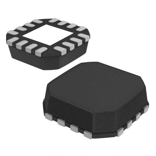
| 供应商器件封装 | 8-SSOP |
| 共模抑制比—最小值 | 60 dB |
| 关闭 | No Shutdown |
| 其它名称 | BA4510FV-E2CT |
| 包装 | 剪切带 (CT) |
| 压摆率 | 5 V/µs |
| 双重电源电压 | +/- 3 V |
| 商标 | ROHM Semiconductor |
| 增益带宽积 | 10MHz |
| 安装类型 | 表面贴装 |
| 安装风格 | SMD/SMT |
| 封装 | Reel |
| 封装/外壳 | 8-LSSOP(0.173",4.40mm 宽) |
| 封装/箱体 | SSOP-B-8 |
| 工作温度 | -20°C ~ 75°C |
| 工作电源电压 | 2 V to 7 V, +/- 1 V to +/- 3.5 V |
| 工厂包装数量 | 2500 |
| 技术 | Bipolar |
| 放大器类型 | 通用 |
| 最大双重电源电压 | +/- 3.5 V |
| 最大工作温度 | + 75 C |
| 最小双重电源电压 | +/- 1 V |
| 最小工作温度 | - 20 C |
| 标准包装 | 1 |
| 电压-电源,单/双 (±) | 2 V ~ 7 V, ±1 V ~ 3.5 V |
| 电压-输入失调 | 1mV |
| 电流-电源 | 5mA |
| 电流-输入偏置 | 80nA |
| 电流-输出/通道 | 10mA |
| 电源电流 | 5 mA |
| 电路数 | 2 |
| 转换速度 | 5 V/us |
| 输入偏压电流—最大 | 500 nA |
| 输入补偿电压 | 6 mV |
| 输出类型 | - |
| 通道数量 | 2 Channel |


- 商务部:美国ITC正式对集成电路等产品启动337调查
- 曝三星4nm工艺存在良率问题 高通将骁龙8 Gen1或转产台积电
- 太阳诱电将投资9.5亿元在常州建新厂生产MLCC 预计2023年完工
- 英特尔发布欧洲新工厂建设计划 深化IDM 2.0 战略
- 台积电先进制程称霸业界 有大客户加持明年业绩稳了
- 达到5530亿美元!SIA预计今年全球半导体销售额将创下新高
- 英特尔拟将自动驾驶子公司Mobileye上市 估值或超500亿美元
- 三星加码芯片和SET,合并消费电子和移动部门,撤换高东真等 CEO
- 三星电子宣布重大人事变动 还合并消费电子和移动部门
- 海关总署:前11个月进口集成电路产品价值2.52万亿元 增长14.8%


PDF Datasheet 数据手册内容提取
Datasheet Operational Amplifiers Series Low Noise Operational Amplifiers BA4510xxx ●General Description ●Packages W(Typ.) x D(Typ.) x H(Max.) BA4510 is dual operational amplifier with high gain. SOP8 5.00mm x 6.20mm x 1.71mm It has good performance of input referred noise SSOP-B8 3.00mm x 6.40mm x 1.35mm voltage(6nV/ Hz ) and total harmonic TSSOP-B8 3.00mm x 6.40mm x 1.20mm distortion(0.007%). These are suitable for Audio MSOP8 2.90mm x 4.00mm x 0.90mm applications. ●Key Specification ●Features Wide Operating Supply Voltage High voltage gain (split supply) : ±1.0V to ±3.5V Low input referred noise voltage Wide Temperature Range: -20°C to +75°C Low distortion High Slew Rate: 5V/µs(Typ.) Wide operating supply voltage Total Harmonic Distortion: 0.007%(Typ.) Input Referred Noise Voltage: 6nV/ Hz (Typ.) ●Application Audio application Consumer electronics ●Block Diagrams VVCCCC --IINN VOOUTU T ++IINN VVEEEE Figure 1. Simplified schematic ○Product structure:Silicon monolithic integrated circuit ○This product is not designed protection against radioactive rays. www.rohm.com TSZ02201-0RAR1G200080-1-2 © 2012 ROHM Co., Ltd. All rights reserved. 1/19 7.NOV.2012 Rev.001 TSZ22111・14・00
B A4510xxx Datasheet ●Pin Configuration(TOP VIEW) SOP8, SSOP-B8, TSSOP-B8, MSOP8 Pin No. Symbol OUT1 1 8 VCC 1 OUT1 2 -IN1 -IN1 2 CH1 7 OUT2 - + 3 +IN1 4 VEE +IN1 3 6 -IN2 CH2 + - 5 +IN2 VEE 4 5 +IN2 6 -IN2 7 OUT2 8 VCC Package SOP8 SSOP-B8 TSSOP-B8 MSOP8 BA4510F BA4510FV BA4510FVT BA4510FVM ●Ordering Information B A 4 5 1 0 x x x - E2 Part Number Package Packaging and forming specification BA4510xxx F : SOP8 E2: Embossed tape and reel FV : SSOP-B8 (SOP8/SSOP-B8/TSSOP-B8) FVT : TSSOP-B8 TR: Embossed tape and reel FVM : MSOP8 (MSOP8) ●Line-up Operating Supply Slew Rate Orderable Topr Supply Voltage Current Package (Typ.) Part Number (split supply) (Typ.) SOP8 Reel of 2500 BA4510F-E2 SSOP-B8 Reel of 2500 BA4510FV-E2 -20°C to +75°C ±1.0V to ±3.5V 5mA 5V/µs TSSOP-B8 Reel of 2500 BA4510FVT-E2 MSOP8 Reel of 3000 BA4510FVM-TR www.rohm.com TSZ02201-0RAR1G200080-1-2 © 2012 ROHM Co., Ltd. All rights reserved. 2/19 7.NOV.2012 Rev.001 TSZ22111・15・00
B A4510xxx Datasheet ●Absolute Maximum Ratings (Ta=25℃) ○BA4510 Parameter Symbol Ratings Unit Supply Voltage VCC-VEE +10 V SOP8 620*1*5 SSOP-B8 550*2*5 Power dissipation Pd mW TSSOP-B8 500*3*5 MSOP8 470*4*5 Differential Input Voltage *6 Vid VCC-VEE V Input Common-mode Voltage Range Vicm VEE to VCC V Operating Supply Voltage Vopr 2 to 7(±1 to ±3.5) V Operating Temperature Topr -20 to +75 ℃ Storage Temperature Tstg -40 to 125 ℃ Maximum Junction Temperature Tjmax +125 ℃ Note: Absolute maximum rating item indicates the condition which must not be exceeded. Application of voltage in excess of absolute maximum rating or use out absolute maximum rated temperature environment may cause deterioration of characteristics. *1 To use at temperature above Ta=25℃ reduce 6.2mW/℃ *2 To use at temperature above Ta=25℃ reduce 5.5mW/℃ *3 To use at temperature above Ta=25℃ reduce 5.0mW/℃ *4 To use at temperature above Ta=25℃ reduce 4.8mW/℃ *5 Mounted on a FR4 glass epoxy PCB(70mm×70mm×1.6mm). *6 The voltage difference between inverting input and non-inverting input is the differential input voltage. Then input terminal voltage is set to more than VEE. ●Electrical Characteristics ○BA4510 (Unless otherwise specified VCC=+2.5V, VEE=-2.5V, Ta=25℃) Limits Parameter Symbol Unit Condition Min. Typ. Max. Input Offset Voltage *7 Vio - 1 6 mV RS=50Ω Input Offset Current *7 Iio - 2 200 nA - Input Bias Current *8 Ib - 80 500 nA - Supply Current ICC 2.5 5.0 7.5 mA RL=∞, All Op-Amps Maximum Output Voltage(High) VOH +2.0 +2.4 - V RL=10kΩ Maximum Output Voltage(Low) VOL - -2.4 -2.0 V RL=10kΩ Large Signal Voltage Gain Av 60 90 - dB RL≧10kΩ Input Common-mode Voltage Range Vicm -1.3 - +1.5 V - Common-mode Rejection Ratio CMRR 60 80 - dB - Power Supply Rejection Ratio PSRR 60 80 - dB RS=50Ω Slew Rate SR - 5.0 - V/μs Av=1 Av=20dB, RL=10kΩ, Total Harmonic Distortion+ Noise THD+N - 0.007 - % VIN=0.05Vrms, f=1kHz DIN-AUDIO - 6 - RS=100Ω, Vi=0V, f=1kHz nV/ Hz Input Referred Noise Voltage Vn - 0.7 - μVrms DIN-AUDIO Channel Separation CS - - dB R1=100Ω, f=1kHz *7 Absolute value *8 Current direction: Since first input stage is composed with PNP transistor, input bias current flows out of IC. www.rohm.com TSZ02201-0RAR1G200080-1-2 © 2012 ROHM Co., Ltd. All rights reserved. 3/19 7.NOV.2012 Rev.001 TSZ22111・15・00
B A4510xxx Datasheet Description of electrical characteristics Described here are the terms of electric characteristics used in this datasheet. Items and symbols used are also shown. Note that item name and symbol and their meaning may differ from those on another manufacture’s document or general document. 1. Absolute maximum ratings Absolute maximum rating item indicates the condition which must not be exceeded. Application of voltage in excess of absolute maximum rating or use out of absolute maximum rated temperature environment may cause deterioration of characteristics. 1.1 Power supply voltage (VCC/VEE) Indicates the maximum voltage that can be applied between the positive power supply terminal and negative power supply terminal without deterioration or destruction of characteristics of internal circuit. 1.2 Differential input voltage (Vid) Indicates the maximum voltage that can be applied between non-inverting terminal and inverting terminal without deterioration and destruction of characteristics of IC. 1.3 Input common-mode voltage range (Vicm) Indicates the maximum voltage that can be applied to non-inverting terminal and inverting terminal without deterioration or destruction of characteristics. Input common-mode voltage range of the maximum ratings not assure normal operation of IC. When normal operation of IC is desired, the input common-mode voltage of characteristics item must be followed. 1.4 Power dissipation (Pd) Indicates the power that can be consumed by specified mounted board at the ambient temperature 25℃(normal temperature). As for package product, Pd is determined by the temperature that can be permitted by IC chip in the package (maximum junction temperature) and thermal resistance of the package. 2. Electrical characteristics item 2.1 Input offset voltage (Vio) Indicates the voltage difference between non-inverting terminal and inverting terminal. It can be translated into the input voltage difference required for setting the output voltage at 0 V. 2.2 Input offset current (Iio) Indicates the difference of input bias current between non-inverting terminal and inverting terminal. 2.3 Input bias current (Ib) Indicates the current that flows into or out of the input terminal. It is defined by the average of input bias current at non-inverting terminal and input bias current at inverting terminal. 2.4 Input common-mode voltage range(Vicm) Indicates the input voltage range where IC operates normally. 2.5 Large signal voltage gain (Av) Indicates the amplifying rate (gain) of output voltage against the voltage difference between non-inverting terminal and Inverting terminal. It is normally the amplifying rate (gain) with reference to DC voltage. Av = (Output voltage fluctuation) / (Input offset fluctuation) 2.6 Circuit current (ICC) Indicates the IC current that flows under specified conditions and no-load steady status. 2.7 Maximum Output Voltage(High) / Maximum Output Voltage(Low) (VOH/VOL) Indicates the voltage range that can be output by the IC under specified load condition. It is typically divided into maximum output voltage High and low. Maximum output voltage high indicates the upper limit of output voltage. Maximum output voltage low indicates the lower limit. 2.8 Common-mode rejection ratio (CMRR) Indicates the ratio of fluctuation of input offset voltage when in-phase input voltage is changed. It is normally the fluctuation of DC. CMRR = (Change of Input common-mode voltage)/(Input offset fluctuation) 2.9 Power supply rejection ratio (PSRR) Indicates the ratio of fluctuation of input offset voltage when supply voltage is changed. It is normally the fluctuation of DC. PSRR = (Change of power supply voltage) / (Input offset fluctuation) 2.10 Slew Rate (SR) SR is a parameter that shows movement speed of operational amplifier. It indicates rate of variable output voltage as unit time. 2.11 Total harmonic distortion + Noise (THD+N) Indicates the fluctuation of input offset voltage or that of output voltage with reference to the change of output voltage of driven channel. www.rohm.com TSZ02201-0RAR1G200080-1-2 © 2012 ROHM Co., Ltd. All rights reserved. 4/19 7.NOV.2012 Rev.001 TSZ22111・15・00
B A4510xxx Datasheet 2.12 Input referred noise voltage (Vn) Indicates a noise voltage generated inside the operational amplifier equivalent by ideal voltage source connected in series with input terminal. 2.13 Channel separation (CS) Indicates the fluctuation of input offset voltage or that of output voltage with reference to the change of output voltage of driven channel. www.rohm.com TSZ02201-0RAR1G200080-1-2 © 2012 ROHM Co., Ltd. All rights reserved. 5/19 7.NOV.2012 Rev.001 TSZ22111・15・00
B A4510xxx Datasheet ●Typical Performance Curves ○BA4510 800 10 BA4510F -20℃ W] . 600 BA4510FV mA] 8 25℃ m [ ON [ NT 6 PATI 400 RRE 75℃ DISSI BA4510FVT Y CU 4 ER PL OW 200 UP P BA4510FVM S 2 0 0 0 25 50 75 100 125 ±0 ±1 ±2 ±3 ±4 AMBIENT TEMPERATURE [℃] SUPPLY VOLTAGE [V] Figure 2. Figure 3. Derating Curve Supply Current - Supply Voltage 10 3 ±3.5V 2 8 T [mA] ±2.5V GE [V] 1 VOH N 6 A RRE OLT 0 U V C 4 T Y U L ±1.5V P -1 P T P U SU 2 O VOL -2 0 -3 -50 -25 0 25 50 75 100 0.1 1 10 100 1000 10000 AMBIENT TEMPERATURE [℃] LOAD RESISTANCE [kΩ] Figure 4. Figure 5. Supply Current - Ambient Temperature Maximum Output Voltage Swing - Load Resistance (VCC/VEE=2.5V/-2.5V, Ta=25℃) (*) The above data is measurement value of typical sample, it is not guaranteed. www.rohm.com TSZ02201-0RAR1G200080-1-2 © 2012 ROHM Co., Ltd. All rights reserved. 6/19 7.NOV.2012 Rev.001 TSZ22111・15・00
B A4510xxx Datasheet ○BA4510 4 3 3 2 2 V] VOH V] VOH E [ 1 AGE [ 1 TAG LT 0 OL 0 O V UT V -1 UT P P -1 T VOL T OU -2 OU VOL -2 -3 -4 -3 ±1.0 ±1.5 ±2.0 ±2.5 ±3.0 ±3.5 ±4.0 -50 -25 0 25 50 75 100 AMBIENT TEMPERATURE [℃] SUPPLY VOLTAGE [V] Figure 6. Figure 7. Maximum Output Voltage Maximum Output Voltage - Supply Voltage - Ambient Temperature (RL=10kΩ, Ta=25℃) (VCC/VEE=2.5V/-2.5V, RL=10kΩ) 3.0 0.0 2.5 -0.5 GE [V] 2.0 GE [V] -1.0 TA VOH TA OL 1.5 OL -1.5 T V T V VOL U U P 1.0 P -2.0 T T OU OU 0.5 -2.5 0.0 -3.0 0 0.4 0.8 1.2 1.6 2 0 2 4 6 8 10 OUTPUT SOURCE CURRENT [mA] OUTPUT SINK CURRENT [mA] Figure 8. Figure 9. Maximum Output Voltage Maximum Output Voltage - Output Source Current - Output Sink Current (VCC/VEE=2.5V/-2.5V, Ta=25℃) (VCC/VEE=2.5V/-2.5V, Ta=25℃) (*) The above data is measurement value of typical sample, it is not guaranteed. www.rohm.com TSZ02201-0RAR1G200080-1-2 © 2012 ROHM Co., Ltd. All rights reserved. 7/19 7.NOV.2012 Rev.001 TSZ22111・15・00
B A4510xxx Datasheet ○BA4510 2.0 6.0 V] 4.0 V] m m E [ -20°C E [ 1.5 AG 2.0 AG ±1.5V T T L L O O V V 1.0 T 0.0 T SE 75°C 25°C SE ±2.5V F F OF-2.0 OF T T 0.5 U U P P ±3.5V IN-4.0 IN -6.0 0.0 -50 -25 0 25 50 75 100 ±1.0 ±1.5 ±2.0 ±2.5 ±3.0 ±3.5 ±4.0 AMBIENT TEMPERATURE [°C] SUPPLY VOLTAGE [V] Figure 10. Figure 11. Input Offset Voltage - Supply Voltage Input Offset Voltage - Ambient Temperature (Vicm=0V, Vout=0V) (Vicm=0V, Vout=0V) 300 300 250 250 NT [nA] 200 ±2.5V ±3.5V NT [nA] 200 25°C 75°C E E R R R R CU 150 CU 150 S S A A -20°C BI 100 BI 100 T ±1.5V T PU PU IN 50 IN 50 0 0 -50 -25 0 25 50 75 100 ±1.0 ±1.5 ±2.0 ±2.5 ±3.0 ±3.5 ±4.0 AMBIENT TEMPERATURE [°C] SUPPLY VOLTAGE [V] Figure 13. Figure 12. Input Bias Current - Ambient Temperature Input Bias Current - Supply Voltage (Vicm=0V, Vout=0V) (Vicm=0V, Vout=0V) (*) The above data is measurement value of typical sample, it is not guaranteed. www.rohm.com TSZ02201-0RAR1G200080-1-2 © 2012 ROHM Co., Ltd. All rights reserved. 8/19 7.NOV.2012 Rev.001 TSZ22111・15・00
B A4510xxx Datasheet ○BA4510 20 20 A] 15 A] 15 n n T [ 10 25°C T [ 10 N N E E ±2.5V ±1.5V RR 5 - 20°C RR 5 U U C C T 0 T 0 E E S S F -5 F -5 F F O 75°C O ±3.5V UT -10 UT -10 P P IN -15 IN -15 -20 -20 ±1.0 ±1.5 ±2.0 ±2.5 ±3.0 ±3.5 ±4.0 -50 -25 0 25 50 75 100 SUPPLY VOLTAGE [V] AMBIENT TEMPERATURE [°C] Figure 14. Figure 15. Input Offset Current - Supply Voltage Input Offset Current - Ambient Temperature (Vicm=0V, Vout=0V) (Vicm=0V, Vout=0V) 10 120 B] d mV] TIO [ 100 E [ 5 RA G N A O 80 LT TI O C V E T 0 EJ 60 E R OFFS 75℃ PPLY 40 UT -5 SU NP 25℃ ER 20 I W -20℃ O P -10 0 -3 -2 -1 0 1 2 3 -50 -25 0 25 50 75 100 COMMON MODE INPUT VOLTAGE [V] AMBIENT TEMPERATURE [℃] Figure 16. Figure 17. Input Offset Voltage Large Signal Voltage Gain - Common Mode Input Voltage -Ambient Temperature (VCC/VEE=2.5V/-2.5V) (*) The above data is measurement value of typical sample, it is not guaranteed. www.rohm.com TSZ02201-0RAR1G200080-1-2 © 2012 ROHM Co., Ltd. All rights reserved. 9/19 7.NOV.2012 Rev.001 TSZ22111・15・00
B A4510xxx Datasheet ○BA4510 120 120 dB] dB] O [ O [ TI 100 TI 100 A A R R N N O 80 O 80 TI TI C C E E EJ 60 EJ 60 R R E Y D L O 40 P 40 M UP N S MO 20 ER 20 M W O O C 0 P 0 -50 -25 0 25 50 75 100 -50 -25 0 25 50 75 100 AMBIENT TEMPERATURE [°C] AMBIENT TEMPERATURE [℃] Figure 18. Figure 19. Common Mode Rejection Ratio Power Supply Rejection Ratio - Ambient Temperature -Ambient Temperature 10 10 8 8 s] μs] H [V/µ 6 ±3.5V -L [V/ 6 ±3.5V E L- ±2.5V TE H W RAT 4 W RA 4 ±2.5V E LE SL S ±1.5V 2 2 ±1.5V 0 0 -50 -25 0 25 50 75 100 -50 -25 0 25 50 75 100 AMBIENT TEMPERATURE [℃] AMBIENT TEMPERATURE [℃] Figure 21. Figure 20. Slew Rate H-L- Ambient Temperature Slew Rate L-H - Ambient Temperature (*) The above data is measurement value of typical sample, it is not guaranteed. www.rohm.com TSZ02201-0RAR1G200080-1-2 © 2012 ROHM Co., Ltd. All rights reserved. 10/19 7.NOV.2012 Rev.001 TSZ22111・15・00
B A4510xxx Datasheet ○BA4510 1 40 %] N [ GE O A TI 1kHz LT 30 R O O 0.1 V DIST 20Hz OISE Hz] C 20kHz N√ 20 NI D V/ O En M R[ R 0.01 ER A F H E 10 AL T R T U O P T N I 0.001 0 0.01 0.1 1 10 1 10 100 1000 10000 OUTPUT VOLTAGE [Vrms] FREQUENCY [Hz] Figure 22. Figure 23. Total Harmonic Distortion - Output Voltage Equivalent Input Noise Voltage - Frequency (VCC/VEE=2.5V/-2.5V, RL=3kΩ, 80kHz-LPF, Ta=25℃) (VCC/VEE=2.5V/-2.5V) 60 0 50 Phase -30 40 -60 B] eg] d Gain d N [ 30 -90 E [ AI AS G H P 20 -120 10 -150 0 -180 1.1E0+20 2 1 .E10+30 3 1 .E1+040 4 1 .E1+050 5 1 . E1+006 6 1 . E1+0077 FREQUENCY [Hz] Figure 24. Voltage Gain・Phase - Frequency (VCC/VEE=2.5V/-2.5V, Av=40dB, RL=10kΩ) (*) The above data is measurement value of typical sample, it is not guaranteed. www.rohm.com TSZ02201-0RAR1G200080-1-2 © 2012 ROHM Co., Ltd. All rights reserved. 11/19 7.NOV.2012 Rev.001 TSZ22111・15・00
B A4510xxx Datasheet ●Application Information NULL method Condition for Test circuit1 VCC, VEE, EK, Vicm Unit: V calculatio Parameter VF S1 S2 S3 VCC VEE EK Vicm n Input Offset Voltage VF1 ON ON OFF 2.5 -2.5 0 0 1 Input Offset Current VF2 OFF OFF OFF 2.5 -2.5 0 0 2 VF3 OFF ON 0 0 Input Bias Current OFF 2.5 -2.5 3 VF4 ON OFF 0 0 VF5 2.5 -2.5 0 0 Large Signal Voltage Gain ON ON ON 4 VF6 2.5 -2.5 0 0 Common-mode Rejection Ratio (Input VF7 1 -4 0 0 ON ON OFF 5 common-mode Voltage Range) VF8 3.8 -1.2 0 0 Power Supply VF9 1 -1 0 0 ON ON OFF 6 Rejection Ratio VF10 2.5 -2.5 0 0 -Calculation- VF1 1. Input Offset Voltage (Vio) Vio [V] 1 + RF / RS 2. Input Offset Current (Iio) Iio VF2-VF1 [A] Ri ×(1 + RF / RS) VF4-VF3 3. Input Bias Current (Ib) Ib [A] 2×Ri× (1 + RF / RS) ΔEK×(1+RF/RS) 4. Large Signal Voltage Gain (Av) Av 20×Log [dB] VF5-VF6 5. Common-mode Rejection Ration (CMRR) ΔVicm×(1+RF/RS) CMRR 20×Log [dB] VF8-VF7 ΔVcc×(1+RF/RS) 6. Power supply rejection ratio (PSRR) PSRR 20×Log [dB] VF10-VF9 0.1μF RF=50kΩ 0.1μF 500kΩ SW1 VCC EK +15V RS=50Ω 500kΩ Ri=10kΩ DUT Ri=10kΩ NULL SW3 RS=50Ω 1000pF Vicm RL V VF 50kΩ SW2 VEE -15V Figure 25. Test circuit1 (one channel only) www.rohm.com TSZ02201-0RAR1G200080-1-2 © 2012 ROHM Co., Ltd. All rights reserved. 12/19 7.NOV.2012 Rev.001 TSZ22111・15・00
B A4510xxx Datasheet Switch Condition for Test Circuit 2 SW No. SW1 SW2 SW3 SW4 SW5 SW6 SW7 SW8 SW9 SW10 SW11SW12SW13SW14 Supply Current OFF OFF OFF ON OFF ON OFF OFF OFF OFF OFF OFF OFF OFF Maximum Output Voltage(High) OFF OFF ON OFF OFF ON OFF OFF ON OFF OFF OFF ON OFF Maximum Output Voltage(Low) OFF OFF ON OFF OFF ON OFF OFF OFF OFF OFF OFF ON OFF Output Source Current OFF OFF ON OFF OFF ON OFF OFF OFF OFF OFF OFF OFF ON Output Sink Current OFF OFF ON OFF OFF ON OFF OFF OFF OFF OFF OFF OFF ON Slew Rate OFF OFF OFF ON OFF OFF OFF ON ON ON OFF OFF OFF OFF Gain Bandwidth Product OFF ON OFF OFF ON ON OFF OFF ON ON OFF OFF OFF OFF Equivalent Input Noise Voltage ON OFF OFF OFF ON ON OFF OFF OFF OFF ON OFF OFF OFF SW4 Input voltage SW5 R2 VH VCC A - VL t SW1 SW2 SW3 + Time SW6 SW7 SW8 SW9 SW10 SW11 SW12 SW13 SW14 Output voltage RS R1 VEE 90% SR=ΔV/Δt VH C A ~ VIN- VIN+~ RL CL ~V V VOUT ΔV 10% VL Δt t Figure 26. Test Circuit 2 (each Op-Amp) Time Figure 27. Slew Rate Input Waveform VCC VCC OTHER R1//R2 R1//R2 CH VEE VEE R1 R2 R1 R2 VOUT1 VIN V V VOUT2 =0.5[Vrms] 100×VOUT1 CS=20×log VOUT2 Figure 28. Test Circuit 3 (Channel Separation) (VCC=+2.5V. VEE=-2.5V, R1=100Ω, R2=10kΩ) www.rohm.com TSZ02201-0RAR1G200080-1-2 © 2012 ROHM Co., Ltd. All rights reserved. 13/19 7.NOV.2012 Rev.001 TSZ22111・15・00
B A4510xxx Datasheet ●Power Dissipation Power dissipation(total loss) indicates the power that can be consumed by IC at Ta=25℃(normal temperature). IC is heated when it consumed power, and the temperature of IC chip becomes higher than ambient temperature. The temperature that can be accepted by IC chip depends on circuit configuration, manufacturing process, and consumable power is limited. Power dissipation is determined by the temperature allowed in IC chip(maximum junction temperature) and thermal resistance of package(heat dissipation capability). The maximum junction temperature is typically equal to the maximum value in the storage temperature range. Heat generated by consumed power of IC radiates from the mold resin or lead frame of the package. The parameter which indicates this heat dissipation capability(hardness of heat release)is called thermal resistance, represented by the symbol θja℃/W. The temperature of IC inside the package can be estimated by this thermal resistance. Figure 29. (a) shows the model of thermal resistance of the package. Thermal resistance θja, ambient temperature Ta, maximum junction temperature Tjmax, and power dissipation Pd can be calculated by the equation below: θja = (Tjmax-Ta) / Pd ℃/W ・・・・・ (Ⅰ) Derating curve in Figure 29. (b) indicates power that can be consumed by IC with reference to ambient temperature. Power that can be consumed by IC with reference to ambient temperature. Power that can be consumed by IC begins to attenuate at certain ambient temperature. This gradient is determined by thermal resistance θja. Thermal resistance θja depends on chip size, power consumption, package, ambient temperature, package condition, wind velocity, etc even when the same of package is used. Thermal reduction curve indicates a reference value measured at a specified condition. Figure 30. (c) show a derating curve for an example of BA4510. Powe rL SdIisのs消ipa費ti電on力 o f[ WL]SI [W] θja=(Tjmax-Ta)/Pd ℃/W Pd (max) P2 θja2 < θja1 Ambie周nt囲 te温m度pe rTaat u[℃re] Ta [℃] θ' ja2 P1 θ ja2 Tj ' (max) Tj (max) θ' ja1 θ ja1 Chip suチrfッaプce表 te面m温p度er a Ttuj [r℃e ]Tj [℃] Power dissipation P [W] 0 25 50 75 100 125 150 消費電力 P [W] Ambient 周te囲m温pe度ra tTuar e[℃ T]a [℃] (a) Thermal resistance (b) Derating curve Figure 29. Thermal resistance and derating curve 800 W] . 600 620mW(*9) BA4510F m 550mW(*10) BA4510FV N [ 500mW(*11) O PATI 400 470mW(*12) SI S DI ER B A4510FV W 200 O P BA4510FVM 0 0 25 50 75 100 125 AMBIENT TEMPERATURE [℃] (c)BA4510 Derating curve (*9) (*10) (*11) (*12) Unit 6.2 5.5 5.0 4.8 mW/℃ When using the unit above Ta=25℃, subtract the value above per degree℃. Permissible dissipation is the value. Permissible dissipation is the value when FR4 glass epoxy board 70mm ×70mm ×1.6mm (cooper foil area below 3%) is mounted. Figure 30. Derating curve www.rohm.com TSZ02201-0RAR1G200080-1-2 © 2012 ROHM Co., Ltd. All rights reserved. 14/19 7.NOV.2012 Rev.001 TSZ22111・15・00
B A4510xxx Datasheet Application examples ○Voltage follower Voltage gain is 0 dB. This circuit controls output voltage (Vout) equal input VCC voltage (Vin), and keeps Vout with stable because of high input impedance and low output impedance. Vout is shown next expression. Vout=Vin Vout Vin VEE Figure 31. Voltage follower circuit ○Inverting amplifier R2 For inverting amplifier, Vin is amplified by voltage gain decided R1 and R2, and phase reversed voltage is VCC output. Vout is shown next expression. Vout=-(R2/R1)・Vin R1 Vin Input impedance is R1. Vout R1//R2 VEE Figure 32. Inverting amplifier circuit ○Non-inverting amplifier R1 R2 For non-inverting amplifier, Vin is amplified by voltage gain decided R1 and R2, and phase is same with Vin. VCC Vout is shown next expression. Vout=(1 + R2/R1)・Vin This circuit performs high input impedance because Input impedance is operational amplifier’s input Impedance. Vout Vin VEE Figure 33. Non-inverting amplifier circuit www.rohm.com TSZ02201-0RAR1G200080-1-2 © 2012 ROHM Co., Ltd. All rights reserved. 15/19 7.NOV.2012 Rev.001 TSZ22111・15・00
B A4510xxx Datasheet ●Operational Notes VCC 1) Processing of unused circuit It is recommended to apply connection (see the Figure 34.) and set the non + inverting input terminal at the potential within input common-mode voltage range Connect - (Vicm), for any unused circuit. to Vicm Vicm 2) Input voltage VEE Please note that the circuit operates normally only when the input voltage is within the common mode input voltage range of the electric characteristics. Figure 34. The example of application circuit for unused op-amp 3) Maximum output voltage Because the output voltage range becomes narrow as the output current VCC Increases, design the application with margin by considering changes in protection electrical characteristics and temperature characteristics. + resistor 4) Short-circuit of output terminal - When output terminal and VCC or VEE terminal are shorted, excessive Output current may flow under some conditions, and heating may destroy IC. It is necessary to connect a resistor as shown in Figure 35. thereby protecting against VEE load shorting. 5) Power supply (split supply / single supply) in used Op-amp operates when specified voltage is applied between VCC and VEE. Therefore, the single supply Op-Amp can be used for double supply Op-Amp as well. Figure 35. The example of output short protection 6) Power dissipation (Pd) Use a thermal design that allows for a sufficient margin in light of the power dissipation (Pd) in actual operating conditions. 7) Short-circuit between pins and wrong mounting Pay attention to the assembly direction of the ICs. Wrong mounting direction or shorts between terminals, GND, or other components on the circuits, can damage the IC. 8) Use in strong electromagnetic field Using the ICs in strong electromagnetic field can cause operation malfunction. 9) Radiation This IC is not designed to be radiation-resistant. 10) Handing of IC When stress is applied to IC because of deflection or bend of board, the characteristics may fluctuate due to piezo resistance effects. 11) Inspection on set board During testing, turn on or off the power before mounting or dismounting the board from the test Jig. Do not power up the board without waiting for the output capacitors to discharge. The capacitors in the low output impedance terminal can stress the device. Pay attention to the electro static voltages during IC handling, transportation, and storage. 12) Output capacitor When VCC terminal is shorted to VEE (GND) potential and an electric charge has accumulated on the external capacitor, connected to output terminal, accumulated charge may be discharged VCC terminal via the parasitic element within the circuit or terminal protection element. The element in the circuit may be damaged (thermal destruction). When using this IC for an application circuit where there is oscillation, output capacitor load does not occur, as when using this IC as a voltage comparator. Set the capacitor connected to output terminal below 0.1μF in order to prevent damage to IC. Status of this document The Japanese version of this document is formal specification. A customer may use this translation version only for a reference to help reading the formal version. If there are any differences in translation version of this document formal version takes priority. www.rohm.com TSZ02201-0RAR1G200080-1-2 © 2012 ROHM Co., Ltd. All rights reserved. 16/19 7.NOV.2012 Rev.001 TSZ22111・15・00
B A4510xxx Datasheet ●Physical Dimensions Tape and Reel Information SOP8 <Tape and Reel information> 5.0±0.2 (MAX 5.35 include BURR) Tape Embossed carrier tape 4°+−64°° Quantity 2500pcs 8 7 6 5 ±6.20.3 ±4.40.2 0.3MIN ±0.90.15 Dofi rfeecetdion E(2Treheel odnir ethcteio lne fits h tahned 1 apnind oyfo pur opduull cot uist tahte t htaep uep opne rt hleef tr iwghhte hna ynodu hold ) 1 2 3 4 0.595 ±1.50.1 S 0.17-+00..015 0.1 S 0.11 1.27 Direction of feed 0.42±0.1 1pin (Unit : mm) Reel ∗ Order quantity needs to be multiple of the minimum quantity. SSOP-B8 3.0±0.2 <Tape and Reel information> (MAX 3.35 include BURR) 8 7 6 5 Tape Embossed carrier tape Quantity 2500pcs E2 Direction ±0.3±0.2 of feed (Treheel odnir ethcteio lne fits h tahned 1 apnind oyfo pur opduull cot uist tahte t htaep uep opne rt hleef tr iwghhte hna ynodu hold ) 6.44.4 N MI 0.3 1 2 3 4 ±1.150.1 S 0.15±0.1 0.1 S 0.1(0.52) 0.65 0.22+−00..0046 0.08M (Unit : mm) Reel 1∗p Oinrder quantity needs to be multipDlei roef cthtieo mn ionifm feumed quantity. TSSOP-B8 <Tape and Reel information> 3.0±0.1 (MAX 3.35 include BURR) 4 ± 4 Tape Embossed carrier tape 8 7 6 5 Quantity 3000pcs E2 ±0.2±0.1 Dofi rfeecetdion (The direction is the 1pin of product is at the upper left when you hold ) 6.44.4 0.15 reel on the left hand and you pull out the tape on the right hand ± 0.5 0.2 1 2 3 4 ±1.0 1PIN MARK +0.05 1.2MAX±1.00.05 ±0.10.050.502.565 0.245+−000...000845SS 00.0.184M5−0.03 1pin Direction of feed (Unit : mm) Reel ∗ Order quantity needs to be multiple of the minimum quantity. MSOP8 <Tape and Reel information> 2.9±0.1 (MAX 3.25 include BURR) Tape Embossed carrier tape ±4.00.2 ±2.80.1 8765 4°+−64°° ±0.290.15 ±0.60.2 QDofiu rfeaecnettdiiotyn 3T(0RTre0he0elp odcnirs ethcetio lenf tis h tahned 1 apnind oyfo pur opduull cot uist tahte t htaep uep opne rt hrieg hritg whth heann ydou hold ) 1 234 1PIN MARK +0.05 1pin 0.475 0.145−0.03 S X A M 0.9 0.22+−00..0045 ±0.750.05 ±0.080.05 0.65 0.08S Direction of feed (Unit : mm) Reel ∗ Order quantity needs to be multiple of the minimum quantity. www.rohm.com TSZ02201-0RAR1G200080-1-2 © 2012 ROHM Co., Ltd. All rights reserved. 17/19 7.NOV.2012 Rev.001 TSZ22111・15・00
B A4510xxx Datasheet ●Marking Diagrams SOP8(TOP VIEW) SSOP-B8(TOP VIEW) Part Number Marking Part Number Marking LOT Number LOT Number 1PIN MARK 1PIN MARK TSSOP-B8(TOP VIEW) Part Number Marking MSOP8(TOP VIEW) Part Number Marking LOT Number LOT Number 1PIN MARK 1PIN MARK Product Name Package Type Marking F SOP8 FV SSOP-B8 BA4510 4510 FVT TSSOP-B8 FVM MSOP8 ●Land pattern data all dimensions in mm Land pitch Land space Land length Land width PKG e MIE ≧ℓ 2 b2 SOP8 1.27 4.60 1.10 0.76 SSOP-B8 0.65 4.60 1.20 0.35 TSSOP-B8 0.65 4.60 1.20 0.35 MSOP8 0.65 2.62 0.99 0.35 MIE e 2 b ℓ2 www.rohm.com TSZ02201-0RAR1G200080-1-2 © 2012 ROHM Co., Ltd. All rights reserved. 18/19 7.NOV.2012 Rev.001 TSZ22111・15・00
B A4510xxx Datasheet ●Revision History Date Revision Changes 2012.11.7 001 New Release www.rohm.com TSZ02201-0RAR1G200080-1-2 © 2012 ROHM Co., Ltd. All rights reserved. 19/19 7.NOV.2012 Rev.001 TSZ22111・15・00
DDaattaasshheeeett Notice Precaution on using ROHM Products 1. Our Products are designed and manufactured for application in ordinary electronic equipments (such as AV equipment, OA equipment, telecommunication equipment, home electronic appliances, amusement equipment, etc.). If you intend to use our Products in devices requiring extremely high reliability (such as medical equipment (Note 1), transport equipment, traffic equipment, aircraft/spacecraft, nuclear power controllers, fuel controllers, car equipment including car accessories, safety devices, etc.) and whose malfunction or failure may cause loss of human life, bodily injury or serious damage to property (“Specific Applications”), please consult with the ROHM sales representative in advance. Unless otherwise agreed in writing by ROHM in advance, ROHM shall not be in any way responsible or liable for any damages, expenses or losses incurred by you or third parties arising from the use of any ROHM’s Products for Specific Applications. (Note1) Medical Equipment Classification of the Specific Applications JAPAN USA EU CHINA CLASSⅢ CLASSⅡb CLASSⅢ CLASSⅢ CLASSⅣ CLASSⅢ 2. ROHM designs and manufactures its Products subject to strict quality control system. However, semiconductor products can fail or malfunction at a certain rate. Please be sure to implement, at your own responsibilities, adequate safety measures including but not limited to fail-safe design against the physical injury, damage to any property, which a failure or malfunction of our Products may cause. The following are examples of safety measures: [a] Installation of protection circuits or other protective devices to improve system safety [b] Installation of redundant circuits to reduce the impact of single or multiple circuit failure 3. Our Products are designed and manufactured for use under standard conditions and not under any special or extraordinary environments or conditions, as exemplified below. Accordingly, ROHM shall not be in any way responsible or liable for any damages, expenses or losses arising from the use of any ROHM’s Products under any special or extraordinary environments or conditions. If you intend to use our Products under any special or extraordinary environments or conditions (as exemplified below), your independent verification and confirmation of product performance, reliability, etc, prior to use, must be necessary: [a] Use of our Products in any types of liquid, including water, oils, chemicals, and organic solvents [b] Use of our Products outdoors or in places where the Products are exposed to direct sunlight or dust [c] Use of our Products in places where the Products are exposed to sea wind or corrosive gases, including Cl2, H2S, NH3, SO2, and NO2 [d] Use of our Products in places where the Products are exposed to static electricity or electromagnetic waves [e] Use of our Products in proximity to heat-producing components, plastic cords, or other flammable items [f] Sealing or coating our Products with resin or other coating materials [g] Use of our Products without cleaning residue of flux (even if you use no-clean type fluxes, cleaning residue of flux is recommended); or Washing our Products by using water or water-soluble cleaning agents for cleaning residue after soldering [h] Use of the Products in places subject to dew condensation 4. The Products are not subject to radiation-proof design. 5. Please verify and confirm characteristics of the final or mounted products in using the Products. 6. In particular, if a transient load (a large amount of load applied in a short period of time, such as pulse. is applied, confirmation of performance characteristics after on-board mounting is strongly recommended. Avoid applying power exceeding normal rated power; exceeding the power rating under steady-state loading condition may negatively affect product performance and reliability. 7. De-rate Power Dissipation (Pd) depending on Ambient temperature (Ta). When used in sealed area, confirm the actual ambient temperature. 8. Confirm that operation temperature is within the specified range described in the product specification. 9. ROHM shall not be in any way responsible or liable for failure induced under deviant condition from what is defined in this document. Precaution for Mounting / Circuit board design 1. When a highly active halogenous (chlorine, bromine, etc.) flux is used, the residue of flux may negatively affect product performance and reliability. 2. In principle, the reflow soldering method must be used; if flow soldering method is preferred, please consult with the ROHM representative in advance. For details, please refer to ROHM Mounting specification Notice - GE Rev.002 © 2014 ROHM Co., Ltd. All rights reserved.
DDaattaasshheeeett Precautions Regarding Application Examples and External Circuits 1. If change is made to the constant of an external circuit, please allow a sufficient margin considering variations of the characteristics of the Products and external components, including transient characteristics, as well as static characteristics. 2. You agree that application notes, reference designs, and associated data and information contained in this document are presented only as guidance for Products use. Therefore, in case you use such information, you are solely responsible for it and you must exercise your own independent verification and judgment in the use of such information contained in this document. ROHM shall not be in any way responsible or liable for any damages, expenses or losses incurred by you or third parties arising from the use of such information. Precaution for Electrostatic This Product is electrostatic sensitive product, which may be damaged due to electrostatic discharge. Please take proper caution in your manufacturing process and storage so that voltage exceeding the Products maximum rating will not be applied to Products. Please take special care under dry condition (e.g. Grounding of human body / equipment / solder iron, isolation from charged objects, setting of Ionizer, friction prevention and temperature / humidity control). Precaution for Storage / Transportation 1. Product performance and soldered connections may deteriorate if the Products are stored in the places where: [a] the Products are exposed to sea winds or corrosive gases, including Cl2, H2S, NH3, SO2, and NO2 [b] the temperature or humidity exceeds those recommended by ROHM [c] the Products are exposed to direct sunshine or condensation [d] the Products are exposed to high Electrostatic 2. Even under ROHM recommended storage condition, solderability of products out of recommended storage time period may be degraded. It is strongly recommended to confirm solderability before using Products of which storage time is exceeding the recommended storage time period. 3. Store / transport cartons in the correct direction, which is indicated on a carton with a symbol. Otherwise bent leads may occur due to excessive stress applied when dropping of a carton. 4. Use Products within the specified time after opening a humidity barrier bag. Baking is required before using Products of which storage time is exceeding the recommended storage time period. Precaution for Product Label QR code printed on ROHM Products label is for ROHM’s internal use only. Precaution for Disposition When disposing Products please dispose them properly using an authorized industry waste company. Precaution for Foreign Exchange and Foreign Trade act Since our Products might fall under controlled goods prescribed by the applicable foreign exchange and foreign trade act, please consult with ROHM representative in case of export. Precaution Regarding Intellectual Property Rights 1. All information and data including but not limited to application example contained in this document is for reference only. ROHM does not warrant that foregoing information or data will not infringe any intellectual property rights or any other rights of any third party regarding such information or data. ROHM shall not be in any way responsible or liable for infringement of any intellectual property rights or other damages arising from use of such information or data.: 2. No license, expressly or implied, is granted hereby under any intellectual property rights or other rights of ROHM or any third parties with respect to the information contained in this document. Other Precaution 1. This document may not be reprinted or reproduced, in whole or in part, without prior written consent of ROHM. 2. The Products may not be disassembled, converted, modified, reproduced or otherwise changed without prior written consent of ROHM. 3. In no event shall you use in any way whatsoever the Products and the related technical information contained in the Products or this document for any military purposes, including but not limited to, the development of mass-destruction weapons. 4. The proper names of companies or products described in this document are trademarks or registered trademarks of ROHM, its affiliated companies or third parties. Notice - GE Rev.002 © 2014 ROHM Co., Ltd. All rights reserved.
DDaattaasshheeeett General Precaution 1. Before you use our Products, you are requested to carefully read this document and fully understand its contents. ROHM shall not be in any way responsible or liable for failure, malfunction or accident arising from the use of a ny ROHM’s Products against warning, caution or note contained in this document. 2. All information contained in this document is current as of the issuing date and subj ect to change without any prior notice. Before purchasing or using ROHM’s Products, please confirm the latest information with a ROHM sale s representative. 3. The information contained in this document is provided on an “as is” basis and ROHM does not warrant that all information contained in this document is accurate an d/or error-free. ROHM shall not be in any way responsible or liable for any damages, expenses or losses incurred by you or third parties resulting from inaccuracy or errors of or concerning such information. Notice – WE Rev.001 © 2014 ROHM Co., Ltd. All rights reserved.