ICGOO在线商城 > LM3208UR/NOPB

 Datasheet下载
- 型号: LM3208UR/NOPB
- 制造商: Texas Instruments
- 库位|库存: xxxx|xxxx
- 要求:
| 数量阶梯 | 香港交货 | 国内含税 |
| +xxxx | $xxxx | ¥xxxx |
查看当月历史价格
查看今年历史价格
LM3208UR/NOPB产品简介:
ICGOO电子元器件商城为您提供LM3208UR/NOPB由Texas Instruments设计生产,在icgoo商城现货销售,并且可以通过原厂、代理商等渠道进行代购。 提供LM3208UR/NOPB价格参考以及Texas InstrumentsLM3208UR/NOPB封装/规格参数等产品信息。 你可以下载LM3208UR/NOPB参考资料、Datasheet数据手册功能说明书, 资料中有LM3208UR/NOPB详细功能的应用电路图电压和使用方法及教程。
| 参数 | 数值 |
| 产品目录 | 集成电路 (IC)半导体 |
| 描述 | IC CONV DC-DC STP-DN ADJ 8SMD稳压器—开关式稳压器 |
| 产品分类 | |
| 品牌 | Texas Instruments |
| 产品手册 | http://www.ti.com/litv/SNVS404A |
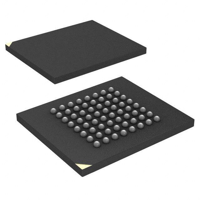
| 产品图片 |
|
| rohs | 符合RoHS无铅 / 符合限制有害物质指令(RoHS)规范要求 |
| 产品系列 | 电源管理 IC,稳压器—开关式稳压器,Texas Instruments LM3208UR/NOPB- |
| 数据手册 | |
| 产品型号 | LM3208UR/NOPB |
| 产品种类 | 稳压器—开关式稳压器 |
| 供应商器件封装 | 8-TuSMD |
| 其它名称 | LM3208UR/NOPBDKR |
| 包装 | Digi-Reel® |
| 商标 | Texas Instruments |
| 安装类型 | 表面贴装 |
| 安装风格 | SMD/SMT |
| 封装 | Reel |
| 封装/外壳 | 8-WFBGA |
| 封装/箱体 | DSBGA-8 |
| 工作温度 | -30°C ~ 85°C |
| 工厂包装数量 | 250 |
| 应用 | 转换器,RF 功率放大器 |
| 开关频率 | 2 MHz |
| 最大工作温度 | + 85 C |
| 最大输入电压 | 42 V |
| 最小工作温度 | - 30 C |
| 标准包装 | 1 |
| 电压-输入 | 2.7 V ~ 5.5 V |
| 电压-输出 | 0.8 V ~ 3.6 V |
| 类型 | Voltage Converter |
| 系列 | LM3208 |
| 输入电压 | 2.7 V to 5.5 V |
| 输出数 | 1 |
| 输出电压 | 800 mV to 3.6 V |
| 输出电流 | 650 mA |
| 输出端数量 | 1 Output |
| 配用 | /product-detail/zh/LM3208TLEV/LM3208TLEV-ND/1640656 |


- 商务部:美国ITC正式对集成电路等产品启动337调查
- 曝三星4nm工艺存在良率问题 高通将骁龙8 Gen1或转产台积电
- 太阳诱电将投资9.5亿元在常州建新厂生产MLCC 预计2023年完工
- 英特尔发布欧洲新工厂建设计划 深化IDM 2.0 战略
- 台积电先进制程称霸业界 有大客户加持明年业绩稳了
- 达到5530亿美元!SIA预计今年全球半导体销售额将创下新高
- 英特尔拟将自动驾驶子公司Mobileye上市 估值或超500亿美元
- 三星加码芯片和SET,合并消费电子和移动部门,撤换高东真等 CEO
- 三星电子宣布重大人事变动 还合并消费电子和移动部门
- 海关总署:前11个月进口集成电路产品价值2.52万亿元 增长14.8%


PDF Datasheet 数据手册内容提取
LM3208 www.ti.com SNVS404B–APRIL2006–REVISEDMARCH2013 LM3208 650mA Miniature, Adjustable, Step-Down DC-DC Converter for RF Power Amplifiers CheckforSamples:LM3208 FEATURES DESCRIPTION 1 • 2MHz(typ.)PWMSwitchingFrequency The LM3208 is a DC-DC converter optimized for 2 powering RF power amplifiers (PAs) from a single • OperatesfromaSingleLi-IonCell(2.7Vto Lithium-Ion cell. However, it may be used in many 5.5V) other applications. It steps down an input voltage in • AdjustableOutputVoltage(0.8Vto3.6V) the range from 2.7V to 5.5V to an adjustable output • FastOutputVoltageTransient(0.8Vto3.4Vin voltage of 0.8V to 3.6V. Output voltage is set by using a V analog input to control power levels and 25µstyp.) CON efficiencyoftheRFPA. • 650mAMaximumLoadCapability The LM3208 offers superior performance for mobile • HighEfficiency(95%typ.at3.9V ,3.4V at IN OUT phones and similar RF PA applications. Fixed- 400mA) frequency PWM operation minimizes RF interference. • 8-pinDSBGAPackage A shutdown function turns the device off and reduces • CurrentOverloadProtection batteryconsumptionto0.01µA(typ.). • ThermalOverloadProtection TheLM3208isavailableinan8-pinlead-freeDSBGA package. A high switching frequency (2 MHz typ.) APPLICATIONS allows use of tiny surface-mount components. Only three small external surface-mount components, an • CellularPhones inductorandtwoceramiccapacitors,arerequired. • Hand-HeldRadios • RFPCCards • BatteryPoweredRFDevices TYPICAL APPLICATION VIN 2.7V to 5.5V VOUT PVIN VDD 3.3 PH 0.8V to 3.6V SW 10 PF EN VOUT = 2.5 x VCON LM3208 FB 4.7 PF VCON PGND SGND Figure1. LM3208TypicalApplication 1 Pleasebeawarethatanimportantnoticeconcerningavailability,standardwarranty,anduseincriticalapplicationsof TexasInstrumentssemiconductorproductsanddisclaimerstheretoappearsattheendofthisdatasheet. Alltrademarksarethepropertyoftheirrespectiveowners. 2 PRODUCTIONDATAinformationiscurrentasofpublicationdate. Copyright©2006–2013,TexasInstrumentsIncorporated Products conform to specifications per the terms of the Texas Instruments standard warranty. Production processing does not necessarilyincludetestingofallparameters.
LM3208 SNVS404B–APRIL2006–REVISEDMARCH2013 www.ti.com CONNECTION DIAGRAMS SW SW A2 A2 PVINA1 A3 PGND PGND A3 A1 PVIN VDDB1 B3 SGND SGND B3 B1 VDD EN C1 C3 FB FB C3 C1 EN C2 C2 VCON VCON Top View Bottom View Figure2. 8-BumpThinDSBGAPackage,LargeBump PackageNumberYZR0008GNA PINDESCRIPTIONS Pin# Name Description A1 PV PowerSupplyVoltageInputtotheinternalPFETswitch. IN B1 V AnalogSupplyInput. DD C1 EN EnableInput.Setthisdigitalinputhighfornormaloperation.Forshutdown,setthispinlow. C2 V VoltageControlAnaloginput.V controlsV inPWMmode. CON CON OUT C3 FB FeedbackAnalogInput.Connecttotheoutputattheoutputfiltercapacitor. B3 SGND AnalogandControlGround A3 PGND PowerGround A2 SW SwitchnodeconnectiontotheinternalPFETswitchandNFETsynchronousrectifier. ConnecttoaninductorwithasaturationcurrentratingthatexceedsthemaximumSwitchPeakCurrentLimit specificationoftheLM3208. Thesedeviceshavelimitedbuilt-inESDprotection.Theleadsshouldbeshortedtogetherorthedeviceplacedinconductivefoam duringstorageorhandlingtopreventelectrostaticdamagetotheMOSgates. 2 SubmitDocumentationFeedback Copyright©2006–2013,TexasInstrumentsIncorporated ProductFolderLinks:LM3208
LM3208 www.ti.com SNVS404B–APRIL2006–REVISEDMARCH2013 ABSOLUTE MAXIMUM RATINGS (1)(2)(3) V ,PV toSGND −0.2Vto+6.0V DD IN PGNDtoSGND −0.2Vto+0.2V EN,FB,V (SGND−0.2V)to(V +0.2V)w/6.0Vmax CON DD SW (PGND−0.2V)to(PV +0.2V)w/6.0Vmax IN PV toV −0.2Vto+0.2V IN DD ContinuousPowerDissipation(4) InternallyLimited JunctionTemperature(T ) +150°C J-MAX StorageTemperatureRange −65°Cto+150°C MaximumLeadTemperature(Soldering,10sec) +260°C ESDRating(5)(6) HumanBodyModel 2kV MachineModel 200V (1) AbsoluteMaximumRatingsindicatelimitsbeyondwhichdamagetothecomponentmayoccur.OperatingRatingsareconditionsunder whichoperationofthedeviceisensured.OperatingRatingsdonotimplyspecifiedperformancelimits.Forspecifiedperformancelimits andassociatedtestconditions,seetheElectricalCharacteristicstables. (2) AllvoltagesarewithrespecttothepotentialattheGNDpins.TheLM3208isdesignedformobilephoneapplicationswhereturn-onafter power-upiscontrolledbythesystemcontrollerandwhererequirementsforasmallpackagesizeoverruleincreaseddiesizeforinternal UnderVoltageLock-Out(UVLO)circuitry.Thus,itshouldbekeptinshutdownbyholdingtheENpinlowuntiltheinputvoltageexceeds 2.7V. (3) IfMilitary/Aerospacespecifieddevicesarerequired,pleasecontacttheTISalesOffice/Distributorsforavailabilityandspecifications. (4) Internalthermalshutdowncircuitryprotectsthedevicefrompermanentdamage.ThermalshutdownengagesatT =150°C(typ.)and J disengagesatT =125°C(typ.). J (5) TheHumanbodymodelisa100pFcapacitordischargedthrougha1.5kΩresistorintoeachpin.(MIL-STD-8833015.7)Themachine modelisa200pFcapacitordischargeddirectlyintoeachpin. (6) TIrecommendsthatallintegratedcircuitsbehandledwithappropriateprecautions.FailuretoobserveproperESDhandlingprocedures canresultindamage. OPERATING RATINGS(1)(2) InputVoltageRange 2.7Vto5.5V RecommendedLoadCurrent 0mAto650mA JunctionTemperature(T)Range −30°Cto+125°C J AmbientTemperature(T )Range(3) −30°Cto+85°C A (1) AbsoluteMaximumRatingsindicatelimitsbeyondwhichdamagetothecomponentmayoccur.OperatingRatingsareconditionsunder whichoperationofthedeviceisensured.OperatingRatingsdonotimplyspecifiedperformancelimits.Forspecifiedperformancelimits andassociatedtestconditions,seetheElectricalCharacteristicstables. (2) AllvoltagesarewithrespecttothepotentialattheGNDpins.TheLM3208isdesignedformobilephoneapplicationswhereturn-onafter power-upiscontrolledbythesystemcontrollerandwhererequirementsforasmallpackagesizeoverruleincreaseddiesizeforinternal UnderVoltageLock-Out(UVLO)circuitry.Thus,itshouldbekeptinshutdownbyholdingtheENpinlowuntiltheinputvoltageexceeds 2.7V. (3) Inapplicationswherehighpowerdissipationand/orpoorpackagethermalresistanceispresent,themaximumambienttemperaturemay havetobede-rated.Maximumambienttemperature(T )isdependentonthemaximumoperatingjunctiontemperature(T = A-MAX J-MAX-OP 125°C),themaximumpowerdissipationofthedeviceintheapplication(P ),andthejunction-toambientthermalresistanceofthe D-MAX part/packageintheapplication(θ ),asgivenbythefollowingequation:T =T –(θ ×P ). JA A-MAX J-MAX-OP JA D-MAX THERMAL PROPERTIES Junction-to-AmbientThermalResistance(θ ),YZR08Package(1) 100°C/W JA (1) Junction-to-ambientthermalresistance(θ )istakenfromthermalmeasurements,performedundertheconditionsandguidelinesset JA forthintheJEDECstandardJESD51-7.A4layer,4"x4",2/1/1/2oz.CuboardasperJEDECstandardsisusedforthemeasurements. Copyright©2006–2013,TexasInstrumentsIncorporated SubmitDocumentationFeedback 3 ProductFolderLinks:LM3208
LM3208 SNVS404B–APRIL2006–REVISEDMARCH2013 www.ti.com ELECTRICAL CHARACTERISTICS(1)(2)(3) LimitsinstandardtypefaceareforT =T =25°C.Limitsinboldfacetypeapplyoverthefulloperatingambienttemperature A J range(−30°C≤T =T ≤+85°C).Unlessotherwisenoted,allspecificationsapplytotheLM3208with:PV =V =EN= A J IN DD 3.6V. Symbol Parameter Conditions Min Typ Max Units V FeedbackVoltageatminimum V =0.32V(3) FB,MIN CON 0.75 0.80 0.85 V setting V FeedbackVoltageatmaximum V =1.44V,V =4.2V(3) FB,MAX CON IN 3.537 3.600 3.683 V setting I Shutdownsupplycurrent EN=SW=V =0V,(4) 0.01 2 µA SHDN CON I DCbiascurrentintoV V =0V,FB=0V, Q DD NCoOSNwitching(5) 0.6 0.7 mA R Pin-pinresistanceforLargePFET I =200mA,V =0.5V 180 DSON(P) SW CON 140 mΩ 210 R Pin-pinresistanceforSmallPFET I =200mA,V =0.32V 960 mΩ DSON(P) SW CON R Pin-pinresistanceforNFET I =–200mA,V =0.5V 375 DSON(N) SW CON 300 mΩ 450 I LargePFET(L)Switchpeakcurrent V =0.5V(6) LIM CON 985 1100 1200 mA (L_PFET) limit I SmallPFET(S)Switchpeakcurrent V =0.32V(6) LIM CON 650 800 900 mA (S_PFET) limit F Internaloscillatorfrequency 1.8 2.0 2.2 MHz OSC V Logichighinputthreshold 1.2 V IH,EN V Logiclowinputthreshold 0.5 V IL,EN I ENpinpulldowncurrent 5 10 µA PIN,EN V V Thresholdforturningon CON,ON CON 0.15 V switches I V pinleakagecurrent V =1.0V ±1 µA CON CON CON Gain V toV Gain 0.32V≤V ≤1.44V 2.5 V/V CON OUT CON (1) AllvoltagesarewithrespecttothepotentialattheGNDpins.TheLM3208isdesignedformobilephoneapplicationswhereturn-onafter power-upiscontrolledbythesystemcontrollerandwhererequirementsforasmallpackagesizeoverruleincreaseddiesizeforinternal UnderVoltageLock-Out(UVLO)circuitry.Thus,itshouldbekeptinshutdownbyholdingtheENpinlowuntiltheinputvoltageexceeds 2.7V. (2) MinandMaxlimitsarespecifiedbydesign,test,orstatisticalanalysis.Typicalnumbersarenotspecified,butdorepresentthemost likelynorm.DuetothepulsednatureofthetestingT =T fortheelectricalcharacteristicstable. A J (3) TheparametersintheelectricalcharacteristicstablearetestedunderopenloopconditionsatPV =V =3.6Vunlessotherwise IN DD specified.Forperformanceovertheinputvoltagerangeandclosed-loopresults,refertothedatasheetcurves. (4) ShutdowncurrentincludesleakagecurrentofPFET. (5) I specifiedhereiswhenthepartisnotswitching.Foroperatingquiescentcurrentatnoload,refertodatasheetcurves. Q (6) Currentlimitisbuilt-in,fixed,andnotadjustable.ElectricalCharacteristictablereflectsopenloopdata(FB=0Vandcurrentdrawnfrom SWpinrampedupuntilcyclebycyclelimitisactivated).RefertoSYSTEMCHARACTERISTICStableformaximumoutputcurrent. 4 SubmitDocumentationFeedback Copyright©2006–2013,TexasInstrumentsIncorporated ProductFolderLinks:LM3208
LM3208 www.ti.com SNVS404B–APRIL2006–REVISEDMARCH2013 SYSTEM CHARACTERISTICS Thefollowingspectableentriesarespecifiedbydesignprovidingthecomponentvaluesinthetypicalapplicationcircuitare used(L=3.0µH,DCR=0.12Ω,FDKMIPW3226D3R0M;C =10µF,6.3V,0805,TDKC2012X5R0J106K;C =4.7µF, IN OUT 6.3V,0603,TDKC1608X5R0J475M).Theseparametersarenotspecifiedbyproductiontesting.MinandMaxvaluesare specifiedovertheambienttemperaturerangeT =−30°Cto85°C.TypicalvaluesarespecifiedatPV =V =EN=3.6V A IN DD andT =25°Cunlessotherwisespecified. A Symbol Parameter Conditions Min Typ Max Unit T TimeforV torisefrom0.8V V =4.2V,R =5.5Ω RESPONSE OUT IN LOAD 25 40 µs to3.4V(toreach3.35V) TimeforV tofallfrom3.4V V =4.2V,R =15Ω OUT IN LOAD 35 45 µs to0.8V C V inputcapacitance V =1V,V =2.7Vto5.5V, CON CON CON IN 5 10 pF Testfrequency=100kHz C ENinputcapacitance EN=2V,V =2.7Vto5.5V, EN IN 5 10 pF Testfrequency=100kHz V R managementthreshold ThresholdforPFETR tochange CON DSON(P) DSON(P) 0.39 0.42 0.45 V (S>L) from960mΩto140mΩ V R managementthreshold ThresholdforPFETR tochange CON DSON(P) DSON(P) 0.37 0.40 0.43 V (L>S) from140mΩto960mΩ I MaximumOutputCurrent V =2.7Vto5.5V, OUT,MAX IN V =0.45Vto1.44V, 650 mA CON L=MIPW3226D3R0 V =2.7Vto5.5V, IN V =0.32Vto0.45V, 400 mA CON L=MIPW3226D3R0 Linearity Linearityincontrolrange0.32V V =3.9V(1) –3 +3 % IN to1.44V Monotonicinnature −50 +50 mV T Turnontime EN=LowtoHigh,V =4.2V, ON IN (timeforoutputtoreach97%of V =3.4V, OUT 40 60 µs finalvalueafterEnablelowto I ≤1mA OUT hightransition) η Efficiency V =3.6V,V =0.8V,I =90mA 81 % IN OUT OUT V =3.6V,V =1.5V,I =150mA 89 % IN OUT OUT V =3.9V,V =3.4V,I =400mA 95 % IN OUT OUT V _ripple Ripplevoltageat V =2.7Vto4.5V,V =0.8Vto3.4V, OUT IN OUT nopulseskipcondition Differentialvoltage=V –V >1V, 10 mVp-p IN OUT I =0mAto400mA(2) OUT Ripplevoltageat V =5.5Vtodropout,V =3.4V, pulseskipcondition I IN =650mA(2) OUT 60 mVp-p OUT Line_tr Linetransientresponse V =3.6Vto4.2V, IN T =T =10µs, 50 mVpk R F V =0.8V,I =100mA OUT OUT Load_tr Loadtransientresponse V =3.1/3.6/4.5V,V =0.8V, IN OUT 50 mVpk I =50mAto150mA OUT MaxDuty Maximumdutycycle 100 % cycle (1) Linearitylimitsare±3%or±50mVwhicheverislarger. (2) RipplevoltageshouldbemeasuredatC electrodeonawell-designedPCboardandusingthesuggestedinductorandcapacitors. OUT Copyright©2006–2013,TexasInstrumentsIncorporated SubmitDocumentationFeedback 5 ProductFolderLinks:LM3208
LM3208 SNVS404B–APRIL2006–REVISEDMARCH2013 www.ti.com TYPICAL PERFORMANCE CHARACTERISTICS (CircuitinFigure35,PV =V =EN=3.6VandT =25°Cunlessotherwisespecified.). IN DD A QuiescentCurrent ShutdownCurrent vs vs SupplyVoltage Temperature (V =0V,FB=0V,NoSwitching) (V =0V,EN=0V) CON CON Figure3. Figure4. SwitchingFrequency OutputVoltage vs vs Temperature SupplyVoltage (V =1.3V,I =200mA) (V =1.3V) OUT OUT OUT )% 3 1.312 ( NOIT 2 VIN = 5.5V 1.310 IOUT = 50 mA AIRAV YC 1 VIN = 3.6VVIN = 4.2V )V( EGAT 1.308 IOUT = 300 mA N L E 0 O 1.306 U V Q T E U RF -1 PT 1.304 GNIH -2 UO1.302 IOUT = 650 mA CT VIN = 2.7V IW S -3 1.300 -40 -20 0 20 40 60 80 100 2.5 3.0 3.5 4.0 4.5 5.0 5.5 6.0 AMBIENT TEMPERATURE (ºC) SUPPLY VOLTAGE (V) Figure5. Figure6. OutputVoltage OutputVoltage vs vs Temperature Temperature (V =3.6V,V =0.8V) (V =4.2V,V =3.4V) IN OUT IN OUT Figure7. Figure8. 6 SubmitDocumentationFeedback Copyright©2006–2013,TexasInstrumentsIncorporated ProductFolderLinks:LM3208
LM3208 www.ti.com SNVS404B–APRIL2006–REVISEDMARCH2013 TYPICAL PERFORMANCE CHARACTERISTICS (continued) (CircuitinFigure35,PV =V =EN=3.6VandT =25°Cunlessotherwisespecified.). IN DD A CurrentLimit CurrentLimit vs vs Temperature Temperature (LargePFET) (SmallPFET) Figure9. Figure10. V Voltage V Voltage CON CON vs vs OutputVoltage OutputVoltage (R =10Ω) (R =10Ω) LOAD LOAD 4.0 1.0 TA = -30ºC, 25ºC, 85ºC VIN = 4.7V 3.5 VIN = 3.6V, 4.2V, 4.7V, 5.5V 0.8 )V( E 3.0 )V( E VIN = 5.5V G G ATLOV 22..50 ATLOV 0.6 VIN = 4.2V T T U U 0.4 P 1.5 P T T U U O 1.0 O 0.2 VIN = 3.6V 0.5 0.0 0.0 0.0 0.4 0.8 1.2 1.6 0.0 0.1 0.2 0.3 0.4 VCON VOLTAGE (V) VCON VOLTAGE (V) Figure11. Figure12. Efficiency vs ENHighThreshold OutputVoltage vs (V =3.9V) SupplyVoltage IN 100 RLOAD = 10: 96 )% 92 ( Y C NEIC 88 RLOAD = 5: IF FE 84 80 RLOAD = 15: 76 0.0 0.5 1.0 1.5 2.0 2.5 3.0 3.5 4.0 4.5 0 OUTPUT VOLTAGE (V) Figure13. Figure14. Copyright©2006–2013,TexasInstrumentsIncorporated SubmitDocumentationFeedback 7 ProductFolderLinks:LM3208
LM3208 SNVS404B–APRIL2006–REVISEDMARCH2013 www.ti.com TYPICAL PERFORMANCE CHARACTERISTICS (continued) (CircuitinFigure35,PV =V =EN=3.6VandT =25°Cunlessotherwisespecified.). IN DD A Efficiency Efficiency vs vs OutputCurrent OutputCurrent (V =0.8V) (V =3.6V) OUT OUT 100 VIN = 3.9V 98 96 )% 94 ( Y 92 C NEIC 90 VIN = 4.5V IF 88 F E 86 VIN = 5.5V 84 82 80 0 0 100 200 300 400 500 600 700 OUTPUT CURRENT (mA) Figure15. Figure16. Efficiency Efficiency vs vs OutputCurrent OutputCurrent (R Management) (R Management,V =4.5V) DSON DSON IN 90 90 VOUT = 1.0V VIN = 5.5V 85 85 80 80 75 Y (%) 75 VIN = 3.6V Y (%) 70 NC 70 NC 65 VIN= 4.5V, VOUT= 1.05V FFICIE 65 VIN = 2.7V FFICIE 60 VIN= 4.5V, VOUT= 1.0V E E 55 60 VOUT = 1.05V 55 WP(tyFhpEeicTna (Vl9),O6 LU0aT m r=g: e1 ).P.0 FWVE h(Ttey n(p1 iVc4aO0l U)m,T S :=m )1.a.0ll 5V 4550 WP(tyFhpEeicTna (Vl9),O6 LU0aT m r=g: e1 ).P.0 FWVE h(Ttey n(p1 iVc4aO0l U)m,T S :=m )1.a.0ll 5V 50 40 10 100 1000 10 100 1000 OUTPUT CURRENT (mA) OUTPUT CURRENT (mA) DarkcurvesareefficiencyprofilesofeitherlargePFET orsmallPFETwhicheverishigher. Figure17. Figure18. R DSON vs Temperature R vsTemperature DSON (LargePFET,I =200mA) (SmallPFET,I =200mA) SW SW Figure19. Figure20. 8 SubmitDocumentationFeedback Copyright©2006–2013,TexasInstrumentsIncorporated ProductFolderLinks:LM3208
LM3208 www.ti.com SNVS404B–APRIL2006–REVISEDMARCH2013 TYPICAL PERFORMANCE CHARACTERISTICS (continued) (CircuitinFigure35,PV =V =EN=3.6VandT =25°Cunlessotherwisespecified.). IN DD A R V -V DSON IN OUT vs vs Temperature OutputCurrent (N-ch,I =–200mA) (100%DutyCycle) SW Figure21. Figure22. LoadTransientResponse LoadTransientResponse (V =0.8V) (V =4.2V,V =3.4V) OUT IN OUT VOUT 50 mV/DIV 100 mV/DIV AC Coupled VOUT AC Coupled VIN = 3.6V VIN = 4.2V VOUT = 0.8V VOUT = 3.4V IL 200 mA/DIV IL 200 mA/DIV 400 mA 250 mA IOUT IOUT 50 mA 100 mA 10 Ps/DIV 10 Ps/DIV Figure23. Figure24. Startup Startup (V =3.6V,V =1.3V,R =1kΩ) (V =4.2V,V =3.4V,R =5kΩ) IN OUT LOAD IN OUT LOAD Figure25. Figure26. Copyright©2006–2013,TexasInstrumentsIncorporated SubmitDocumentationFeedback 9 ProductFolderLinks:LM3208
LM3208 SNVS404B–APRIL2006–REVISEDMARCH2013 www.ti.com TYPICAL PERFORMANCE CHARACTERISTICS (continued) (CircuitinFigure35,PV =V =EN=3.6VandT =25°Cunlessotherwisespecified.). IN DD A ShutdownResponse LineTransientReponse (V =4.2V,V =3.4V,R =10Ω) (V =3.0Vto3.6V,I =100mA) IN OUT LOAD IN OUT Figure27. Figure28. V TransientResponse TimedCurrentLimitResponse CON (V =4.2V,V =0.32V/1.44V,R =10Ω) (V =3.6V) IN CON LOAD IN Figure29. Figure30. OutputVoltageRipple (V =1.3V) OUT Figure31. 10 SubmitDocumentationFeedback Copyright©2006–2013,TexasInstrumentsIncorporated ProductFolderLinks:LM3208
LM3208 www.ti.com SNVS404B–APRIL2006–REVISEDMARCH2013 TYPICAL PERFORMANCE CHARACTERISTICS (continued) (CircuitinFigure35,PV =V =EN=3.6VandT =25°Cunlessotherwisespecified.). IN DD A OutputVoltageRipple OutputVoltageRippleinPulseSkip (V =3.4V) (V =3.96V,V =3.4V,R =5Ω) OUT IN OUT LOAD Figure32. Figure33. Copyright©2006–2013,TexasInstrumentsIncorporated SubmitDocumentationFeedback 11 ProductFolderLinks:LM3208
LM3208 SNVS404B–APRIL2006–REVISEDMARCH2013 www.ti.com BLOCK DIAGRAM VDD PVIN SMALL LARGE PFET PFET VCON DELAY ERROR LOGIC AMPLIFIER FB CURRENT COMP SW MOSFET OSCILLATOR CONTROL LOGIC FET SIZE CONTROL COMP MAIN CONTROL EN SHUTDOWN CONTROL GND PGND Figure34. FunctionalBlockDiagram OPERATION DESCRIPTION The LM3208 is a simple, step-down DC-DC converter optimized for powering RF power amplifiers (PAs) in mobile phones, portable communicators, and similar battery powered RF devices. It is designed to allow the RF PA to operate at maximum efficiency over a wide range of power levels from a single Li-Ion battery cell. It is based on a current-mode buck architecture, with synchronous rectification for high efficiency. It is designed for a maximum load capability of 650mA when V > 1.05V (typ.) and 400mA when V < 1.00V (typ.) in PWM OUT OUT mode. Maximumloadrangemayvaryfromthisdependingoninputvoltage,outputvoltageandtheinductorchosen. Efficiency is typically around 95% for a 400mA load with 3.4V output, 3.9V input. The LM3208 has an R DSON management scheme to increase efficiency when V ≤ 1V. The output voltage is dynamically programmable OUT from 0.8V to 3.6V by adjusting the voltage on the control pin without the need for external feedback resistors. ThisprolongsbatterylifebychangingthePAsupplyvoltagedynamicallydependingonitstransmittingpower. Additionalfeaturesincludecurrentoverloadprotectionandthermaloverloadshutdown. The LM3208 is constructed using a chip-scale 8-pin DSBGA package. This package offers the smallest possible size, for space-critical applications such as cell phones, where board area is an important design consideration. Use of a high switching frequency (2MHz, typ.) reduces the size of external components. As shown in Figure 1, only three external power components are required for implementation. Use of a DSBGA package requires special design considerations for implementation. (See DSBGA Package Assembly and Use in the Application Information section.) Its fine bump-pitch requires careful board design and precision assembly equipment. Use of this package is best suited for opaque-case applications, where its edges are not subject to high-intensity ambient red or infrared light. In addition, the system controller should set EN low during power-up and other low supplyvoltageconditions.(SeeShutdownModeintheDeviceInformationsection.) 12 SubmitDocumentationFeedback Copyright©2006–2013,TexasInstrumentsIncorporated ProductFolderLinks:LM3208
LM3208 www.ti.com SNVS404B–APRIL2006–REVISEDMARCH2013 VIN 2.7V to 5.5V C1* 10 PF PVIN VDD L1 VOUT 3.3 PH 0.8V to 3.6V SW SYSTEM LM3208 FB CONTROLLER DAC VCON C2 4.7 PF ON/OFF EN SGND PGND * Place C1 close to PVIN Figure35. TypicalOperatingSystemCircuit Circuit Operation Referring to Figure 1 and Figure 34, the LM3208 operates as follows. During the first part of each switching cycle, the control block in the LM3208 turns on the internal PFET (P-channel MOSFET) switch. This allows current to flow from the input through the inductor to the output filter capacitor and load. The inductor limits the currenttoarampwithaslopeofaround(V –V )/L,bystoringenergyinamagneticfield.Duringthesecond IN OUT part of each cycle, the controller turns the PFET switch off, blocking current flow from the input, and then turns the NFET (N-channel MOSFET) synchronous rectifier on. In response, the inductor’s magnetic field collapses, generating a voltage that forces current from ground through the synchronous rectifier to the output filter capacitor and load. As the stored energy is transferred back into the circuit and depleted, the inductor current ramps down with a slope around V / L. The output filter capacitor stores charge when the inductor current is OUT high,andreleasesitwhenlow,smoothingthevoltageacrosstheload. The output voltage is regulated by modulating the PFET switch on time to control the average current sent to the load. The effect is identical to sending a duty-cycle modulated rectangular wave formed by the switch and synchronous rectifier at SW to a low-pass filter formed by the inductor and output filter capacitor. The output voltageisequaltotheaveragevoltageattheSWpin. While in operation, the output voltage is regulated by switching at a constant frequency and then modulating the energy per cycle to control power to the load. Energy per cycle is set by modulating the PFET switch on-time pulse width to control the peak inductor current. This is done by comparing the signal from the current-sense amplifier with a slope compensated error signal from the voltage-feedback error amplifier. At the beginning of eachcycle,theclockturnsonthePFETswitch,causingtheinductorcurrenttorampup.Whenthecurrentsense signal ramps past the error amplifier signal, the PWM comparator turns off the PFET switch and turns on the NFET synchronous rectifier, ending the first part of the cycle. If an increase in load pulls the output down, the error amplifier output increases, which allows the inductor current to ramp higher before the comparator turns off thePFET.Thisincreasestheaveragecurrentsenttotheoutputandadjustsfortheincreaseintheload. Before appearing at the PWM comparator, a slope compensation ramp from the oscillator is subtracted from the errorsignalforstabilityofthecurrentfeedbackloop.TheminimumontimeofPFETis55ns(typ.) Shutdown Mode Setting the EN digital pin low (<0.5V) places the LM3208 in shutdown mode (0.01µA typ.). During shutdown, the PFET switch, NFET synchronous rectifier, reference voltage source, control and bias circuitry of the LM3208 are turnedoff.SettingENhigh(>1.2V)enablesnormaloperation. EN should be set low to turn off the LM3208 during power-up and under voltage conditions when the power supply is less than the 2.7V minimum operating voltage. The LM3208 is designed for compact portable applications, such as mobile phones. In such applications, the system controller determines power supply sequencing and requirements for small package size outweigh the additional size required for inclusion of UVLO (UnderVoltageLock-Out)circuitry. Copyright©2006–2013,TexasInstrumentsIncorporated SubmitDocumentationFeedback 13 ProductFolderLinks:LM3208
LM3208 SNVS404B–APRIL2006–REVISEDMARCH2013 www.ti.com Internal Synchronous Rectification While in PWM mode, the LM3208 uses an internal NFET as a synchronous rectifier to reduce rectifier forward voltage drop and associated power loss. Synchronous rectification provides a significant improvement in efficiency whenever the output voltage is relatively low compared to the voltage drop across an ordinary rectifier diode. The internal NFET synchronous rectifier is turned on during the inductor current down slope in the second part of each cycle. The synchronous rectifier is turned off prior to the next cycle. The NFET is designed to conduct through its intrinsic body diode during transient intervals before it turns on, eliminating the need for an external diode. R Management DSON(P) The LM3208 has a unique R management function to improve efficiency in the low output current region DSON(P) up to 100mA. When the V voltage is less than 0.40V (typ.), the device uses only a small part of the PFET to CON minimize drive loss of the PFET. When V is greater than 0.42V (typ.), the entire PFET is used to minimize CON R loss.Thisthresholdhasabout20mV(typ.)ofhysteresis. DSON(P) V CON,ON The output is disabled when V is below 125mV (typ.). It is enabled when V is above 150mV (typ.). The CON CON thresholdhasabout25mV(typ.)ofhysteresis. Current Limiting A current limit feature allows the LM3208 to protect itself and external components during overload conditions. In PWM mode, an 1100mA (typ.) cycle-by-cycle current limit is normally used when V is above 0.42V (typ.), and CON an 800mA (typ.) is used when V is below 0.40V (typ.). If an excessive load pulls the output voltage down to CON approximately 0.375V, then the device switches to a timed current limit mode when V is above 0.42V (typ.). CON In timed current limit mode the internal PFET switch is turned off after the current comparator trips and the beginning of the next cycle is inhibited for 3.5µs to force the instantaneous inductor current to ramp down to a safe value. The synchronous rectifier is off in timed current limit mode. Timed current limit prevents the loss of currentcontrolseeninsomeproductswhentheoutputvoltageispulledlowinseriousoverloadconditions. Dynamically Adjustable Output Voltage The LM3208 features dynamically adjustable output voltage to eliminate the need for external feedback resistors. Theoutputcanbesetfrom0.8Vto3.6VbychangingthevoltageontheanalogV pin.Thisfeatureisusefulin CON PA applications where peak power is needed only when the handset is far away from the base station or when data is being transmitted. In other instances, the transmitting power can be reduced. Hence the supply voltage to the PA can be reduced, promoting longer battery life. See Setting The Output Voltage in the Application Information section for further details. The LM3208 moves into Pulse Skipping mode when duty cycle is over 92%andtheoutputvoltagerippleincreasesslightly. Thermal Overload Protection TheLM3208hasathermaloverloadprotectionfunctionthatoperatestoprotectitselffromshort-termmisuseand overload conditions. When the junction temperature exceeds around 150°C, the device inhibits operation. Both the PFET and the NFET are turned off in PWM mode. When the temperature drops below 125°C, normal operation resumes. Prolonged operation in thermal overload conditions may damage the device and is consideredbadpractice. APPLICATION INFORMATION SettingTheOutputVoltage The LM3208 features a pin-controlled variable output voltage to eliminate the need for external feedback resistors. It can be programmed for an output voltage from 0.8V to 3.6V by setting the voltage on the V pin, CON asinthefollowingformula: V =2.5xV (1) OUT CON WhenV isbetween0.32Vand1.44V,theoutputvoltagewillfollowproportionallyby2.5timesofV . CON CON 14 SubmitDocumentationFeedback Copyright©2006–2013,TexasInstrumentsIncorporated ProductFolderLinks:LM3208
LM3208 www.ti.com SNVS404B–APRIL2006–REVISEDMARCH2013 If V is over 1.44V (V = 3.6V), sub-harmonic oscillation may occur because of insufficient slope CON OUT compensation. If V voltage is less than 0.32V (V = 0.8V), the output voltage may not be regulated due to CON OUT the required on-time being less than the minimum on-time (55ns). The output voltage can go lower than 0.8V providing a limited V range is used. Refer to datasheet curve (V Voltage vs Output Voltage) for details. This IN CON curve is for a typical part and there could be part-to-part variation for output voltages less than 0.8V over the limited V range. When the control pin voltage is more than 0.15V (typ.), the switches are turned on. When it is IN less than 0.125V (typ.), the switches are turned off. This on/off function has 25mV (typ.) hysteresis. The quiescentcurrentwhen(V =0VandV =Hi)isaround600µA. CON EN EstimationofMaximumOutputCurrentCapability ReferringtoFigure35,theInductorpeaktopeakripplecurrentcanbeestimatedby: I =(V –V )×V /(L1×F ×V ) IND_PP IN OUT OUT SW IN where • Fswisswitchingfrequency (2) Therefore,maximumoutputcurrentcanbecalculatedby: I =I –0.5×I (3) OUT_MAX LIM IND_PP Fortheworstcasecalculation,thefollowingparametersshouldbeused: F (Lowestswitchingfrequency):1.8MHz SW I (Lowestcurrentlimitvalue):985mA LIM L1 (Lowest inductor value): refer to inductor data-sheet. Note that inductance will drop with DC bias current and temperature.Theworstcaseistypicallyat85°C. Forexample,V =4.2V,V =3.2V,L1=2.0µH(Inductancevalueat985mADCbiascurrentand85°C),F = IN OUT SW 1.8MHz,I =985mA. LIM I =212mA (4) IND_PP I =985–106=876mA (5) OUT_MAX The effects of switch, inductor resistance and dead time are ignored. In real application, the ripple current would be 10% to 15% higher than ideal case. This should be taken into account when calculating maximum output current. Special attention needs to be paid that a delta between maximum output current capability and the current limit is necessary to satisfy transient response requirements. In practice, transient response requirements maynotbemetforoutputcurrentgreaterthan650mA. InductorSelection A 3.3µH inductor with saturation current rating over 1200mA and low inductance drop at the full DC bias condition is recommended for almost all applications. The inductor’s DC resistance should be less than 0.2Ω for good efficiency. For low dropout voltage, lower DCR inductors are recommended. The lower limit of acceptable inductance is 1.7µH at 1200mA over the operating temperature range. Full attention should be paid to this limit, because some small inductors show large inductance drops at high DC bias. These cannot be used with the LM3208. FDK MIPW3226D3R0M is an example of an inductor with the lowest acceptable limit (as of Oct./05). Table1suggestssomeinductorsandsuppliers. Table1.SuggestedInductorsAndTheirSuppliers Model Size(WxLxH)[mm] Vendor MIPW3226D3R0M 3.2x2.6x1.0 FDK 1098AS-3R3M 3.0x2.8x1.2 TOKO NR3015T3R3M 3.0x3.0x1.5 Taiyo-Yuden 1098AS-2R7M 3.0x2.8x1.2 TOKO Copyright©2006–2013,TexasInstrumentsIncorporated SubmitDocumentationFeedback 15 ProductFolderLinks:LM3208
LM3208 SNVS404B–APRIL2006–REVISEDMARCH2013 www.ti.com Ifasmallerinductanceinductorisusedintheapplication,theLM3208maybecomeunstableduringlineandload transients,andV transientresponsetimesmaybeaffected. CON Forlow-costapplications,anunshieldedbobbininductorissuggested.Fornoise-criticalapplications,atoroidalor shielded-bobbin inductor should be used. A good practice is to lay out the board with footprints accommodating both types for design flexibility. This allows substitution of a low-noise toroidal inductor, in the event that noise from low-cost bobbin models is unacceptable. Saturation occurs when the magnetic flux density from current through the windings of the inductor exceeds what the inductor’s core material can support with a corresponding magneticfield.Thiscancausepoorefficiency,regulationerrorsorstresstoaDC-DCconverterliketheLM3208. CapacitorSelection The LM3208 is designed for use with ceramic capacitors for its input and output filters. Use a 10µF ceramic capacitor for input and a 4.7µF ceramic capacitor for output. They should maintain at least 50% capacitance at DC bias and temperature conditions. Ceramic capacitor types such as X5R, X7R and B are recommended for both filters. Table 2 lists some suggested part numbers and suppliers. DC bias characteristics of the capacitors must be considered when selecting the voltage rating and case size of the capacitor. If it is necessary to choose a0603-sizecapacitorforC andC ,theoperationoftheLM3208shouldbecarefullyevaluatedonthesystem IN OUT board.Useofmultiple2.2µFor1µFcapacitorsinparallelmayalsobeconsidered. Table2.SuggestedCapacitorsAndTheirSuppliers Model Vendor C2012X5R0J106M,10µF,6.3V TDK C1608X5R0J475M,4.7µF,6.3V TDK 0805ZD475KA4.7µF,10V AVX The input filter capacitor supplies AC current drawn by the PFET switch of the LM3208 in the first part of each cycle and reduces the voltage ripple imposed on the input power source. The output filter capacitor absorbs the AC inductor current, helps maintain a steady output voltage during transient load changes and reduces output voltage ripple. These capacitors must be selected with sufficient capacitance and sufficiently low ESR (Equivalent Series Resistance) to perform these functions. The ESR of the filter capacitors is generally a major factorinvoltageripple. ENPinControl DrivetheENpinusingthesystemcontrollertoturntheLM3208ONandOFF.Useacomparator,Schmidttrigger or logic gate to drive the EN pin. Set EN high (>1.2V) for normal operation and low (<0.5V) for a 0.01µA (typ.) shutdownmode. Set EN low to turn off the LM3208 during power-up and under voltage conditions when the power supply is less than the 2.7V minimum operating voltage. The part is out of regulation when the input voltage is less than 2.7V. The LM3208 is designed for mobile phones where the system controller controls operation mode for maximizing battery life and requirements for small package size outweigh the additional size required for inclusion of UVLO (UnderVoltageLock-Out)circuitry. DSBGAPackageAssemblyandUse Use of the DSBGA package requires specialized board layout, precision mounting and careful re-flow techniques, as detailed in TI Application Note 1112 (SNVA009). Refer to the section Surface Mount Technology (SMD) Assembly Considerations. For best results in assembly, alignment ordinals on the PC board should be used to facilitate placement of the device. The pad style used with DSBGA package must be the NSMD (non- solder mask defined) type. This means that the solder-mask opening is larger than the pad size. This prevents a lip that otherwise forms if the solder-mask and pad overlap, from holding the device off the surface of the board andinterferingwithmounting.SeeApplicationNote1112(SNVA009)forspecificinstructionshowtodothis. 16 SubmitDocumentationFeedback Copyright©2006–2013,TexasInstrumentsIncorporated ProductFolderLinks:LM3208
LM3208 www.ti.com SNVS404B–APRIL2006–REVISEDMARCH2013 The 8-Bump package used for LM3208 has 300micron solder balls and requires 10.82mil pads for mounting on the circuit board. The trace to each pad should enter the pad with a 90°entry angle to prevent debris from being caughtindeepcorners.Initially,thetracetoeachpadshouldbe7milwide,forasectionapproximately7millong, as a thermal relief. Then each trace should neck up or down to its optimal width. The important criterion is symmetry. This ensures the solder bumps on the LM3208 re-flow evenly and that the device solders level to the board. In particular, special attention must be paid to the pads for bumps A1 and A3. Because PGND and PV IN are typically connected to large copper planes, inadequate thermal relief’s can result in late or inadequate re-flow ofthesebumps. The DSBGA package is optimized for the smallest possible size in applications with red or infrared opaque cases. Because the DSBGA package lacks the plastic encapsulation characteristic of larger devices, it is vulnerable to light. Backside metallization and/or epoxy coating, along with front-side shading by the printed circuit board, reduce this sensitivity. However, the package has exposed die edges. In particular, DSBGA devicesaresensitivetolight(intheredandinfraredrange)shiningonthepackage’sexposeddieedges. BoardLayoutConsiderations VIN i Fosc = 2 MHz 2.7V to 5.5V i L1 PVIN VDD 3.3 PH VOUT SW + C1 E EN -10 PF FB C2 + 4.7 PF VCON PGND SGND - C Figure36. CurrentLoop The LM3208 converts higher input voltage to lower output voltage with high efficiency. This is achieved with an inductor-based switching topology. During the first half of the switching cycle, the internal PMOS switch turns on, the input voltage is applied to the inductor, and the current flows from PV line into the output capacitor and the IN loadthroughtheinductor.Duringthesecondhalfcycle,thePMOSturnsoffandtheinternalNMOSturnson.The inductor current continues to flow via the inductor from the device PGND line into the output capacitor and the load. ReferringtoFigure36,apulsecurrentflowsinthelefthandsideloop,andaripplecurrentflowsintherighthand side loop. Board layout and circuit pattern design of these two loops are the key factors for reducing noise radiation and stable operation. In other lines, such as from battery to C1 and C2 to the load, the current is mostly DC current. Therefore, it is not necessary to take so much care. Only pattern width (current capability) and DCR dropconsiderationsareneeded. Copyright©2006–2013,TexasInstrumentsIncorporated SubmitDocumentationFeedback 17 ProductFolderLinks:LM3208
LM3208 SNVS404B–APRIL2006–REVISEDMARCH2013 www.ti.com 3.0 (cid:219)H 4.7 (cid:219)F 10 (cid:219)F Figure37. EvaluationBoardLayout BoardLayoutFlow 1. Minimize C1, PV , and PGND loop. These traces should be as wide and short as possible. This is the IN highestpriority. 2. Minimize L1, C2, SW and PGND loop. These traces also should be wide and short. This is the second priority. 3. The above layout patterns should be placed on the component side of the PCB to minimize parasitic inductance and resistance due to via-holes. It may be a good idea that the SW to L1 path is routed between C1(+) and C1(–) land patterns. If vias are used in these large current paths, multiple via-holes should be usedifpossible. 4. Connect C1(–), C2(–) and PGND with wide GND pattern. This pattern should be short, so C1(–), C2(–), and PGND should be as close as possible. Then connect to a PCB common GND pattern with as many via-holes aspossible. 5. SGND should not connect directly to PGND. Connecting these pins under the device should be avoided. (If possible,connectSGNDtothecommonportofC1(–),C2(–)andPGND.) 6. V should not be connected directly to PV . Connecting these pins under the device should be avoided. It DD IN isgoodideatoconnectV toC1(+)toavoidswitchingnoiseinjectiontotheV line. DD DD 7. The FB line should be protected from noise. It is a good idea to use an inner GND layer (if available) as a shield. NOTE The evaluation board shown in Figure 37 for the LM3208 was designed with these considerations, and it shows good performance. However some aspects have not been optimized because of limitations due to evaluation-specific requirements. The board can beusedasareference.PleasereferquestionstoaTIrepresentative. 18 SubmitDocumentationFeedback Copyright©2006–2013,TexasInstrumentsIncorporated ProductFolderLinks:LM3208
LM3208 www.ti.com SNVS404B–APRIL2006–REVISEDMARCH2013 Copyright©2006–2013,TexasInstrumentsIncorporated SubmitDocumentationFeedback 19 ProductFolderLinks:LM3208
LM3208 SNVS404B–APRIL2006–REVISEDMARCH2013 www.ti.com REVISION HISTORY ChangesfromRevisionA(March2013)toRevisionB Page • ChangedlayoutofNationalDataSheettoTIformat.......................................................................................................... 18 20 SubmitDocumentationFeedback Copyright©2006–2013,TexasInstrumentsIncorporated ProductFolderLinks:LM3208
PACKAGE OPTION ADDENDUM www.ti.com 11-Apr-2013 PACKAGING INFORMATION Orderable Device Status Package Type Package Pins Package Eco Plan Lead/Ball Finish MSL Peak Temp Op Temp (°C) Top-Side Markings Samples (1) Drawing Qty (2) (3) (4) LM3208TL/NOPB ACTIVE DSBGA YZR 8 250 Green (RoHS SNAGCU Level-1-260C-UNLIM -30 to 85 S & no Sb/Br) 33 LM3208TLX/NOPB ACTIVE DSBGA YZR 8 3000 Green (RoHS SNAGCU Level-1-260C-UNLIM -30 to 85 S & no Sb/Br) 33 (1) The marketing status values are defined as follows: ACTIVE: Product device recommended for new designs. LIFEBUY: TI has announced that the device will be discontinued, and a lifetime-buy period is in effect. NRND: Not recommended for new designs. Device is in production to support existing customers, but TI does not recommend using this part in a new design. PREVIEW: Device has been announced but is not in production. Samples may or may not be available. OBSOLETE: TI has discontinued the production of the device. (2) Eco Plan - The planned eco-friendly classification: Pb-Free (RoHS), Pb-Free (RoHS Exempt), or Green (RoHS & no Sb/Br) - please check http://www.ti.com/productcontent for the latest availability information and additional product content details. TBD: The Pb-Free/Green conversion plan has not been defined. Pb-Free (RoHS): TI's terms "Lead-Free" or "Pb-Free" mean semiconductor products that are compatible with the current RoHS requirements for all 6 substances, including the requirement that lead not exceed 0.1% by weight in homogeneous materials. Where designed to be soldered at high temperatures, TI Pb-Free products are suitable for use in specified lead-free processes. Pb-Free (RoHS Exempt): This component has a RoHS exemption for either 1) lead-based flip-chip solder bumps used between the die and package, or 2) lead-based die adhesive used between the die and leadframe. The component is otherwise considered Pb-Free (RoHS compatible) as defined above. Green (RoHS & no Sb/Br): TI defines "Green" to mean Pb-Free (RoHS compatible), and free of Bromine (Br) and Antimony (Sb) based flame retardants (Br or Sb do not exceed 0.1% by weight in homogeneous material) (3) MSL, Peak Temp. -- The Moisture Sensitivity Level rating according to the JEDEC industry standard classifications, and peak solder temperature. (4) Multiple Top-Side Markings will be inside parentheses. Only one Top-Side Marking contained in parentheses and separated by a "~" will appear on a device. If a line is indented then it is a continuation of the previous line and the two combined represent the entire Top-Side Marking for that device. Important Information and Disclaimer:The information provided on this page represents TI's knowledge and belief as of the date that it is provided. TI bases its knowledge and belief on information provided by third parties, and makes no representation or warranty as to the accuracy of such information. Efforts are underway to better integrate information from third parties. TI has taken and continues to take reasonable steps to provide representative and accurate information but may not have conducted destructive testing or chemical analysis on incoming materials and chemicals. TI and TI suppliers consider certain information to be proprietary, and thus CAS numbers and other limited information may not be available for release. In no event shall TI's liability arising out of such information exceed the total purchase price of the TI part(s) at issue in this document sold by TI to Customer on an annual basis. Addendum-Page 1
PACKAGE MATERIALS INFORMATION www.ti.com 26-Mar-2013 TAPE AND REEL INFORMATION *Alldimensionsarenominal Device Package Package Pins SPQ Reel Reel A0 B0 K0 P1 W Pin1 Type Drawing Diameter Width (mm) (mm) (mm) (mm) (mm) Quadrant (mm) W1(mm) LM3208TL/NOPB DSBGA YZR 8 250 178.0 8.4 1.85 2.01 0.76 4.0 8.0 Q1 LM3208TLX/NOPB DSBGA YZR 8 3000 178.0 8.4 1.85 2.01 0.76 4.0 8.0 Q1 PackMaterials-Page1
PACKAGE MATERIALS INFORMATION www.ti.com 26-Mar-2013 *Alldimensionsarenominal Device PackageType PackageDrawing Pins SPQ Length(mm) Width(mm) Height(mm) LM3208TL/NOPB DSBGA YZR 8 250 210.0 185.0 35.0 LM3208TLX/NOPB DSBGA YZR 8 3000 210.0 185.0 35.0 PackMaterials-Page2
MECHANICAL DATA YZR0008xxx D 0.600±0.075 E TLA08XXX (Rev C) D: Max = 1.862 mm, Min =1 .802 mm E: Max = 1.712 mm, Min =1 .652 mm 4215045/A 12/12 NOTES: A.Alllineardimensionsareinmillimeters.DimensioningandtolerancingperASMEY14.5M-1994. B.Thisdrawingissubjecttochangewithoutnotice. www.ti.com
IMPORTANTNOTICEANDDISCLAIMER TIPROVIDESTECHNICALANDRELIABILITYDATA(INCLUDINGDATASHEETS),DESIGNRESOURCES(INCLUDINGREFERENCE DESIGNS),APPLICATIONOROTHERDESIGNADVICE,WEBTOOLS,SAFETYINFORMATION,ANDOTHERRESOURCES“ASIS” ANDWITHALLFAULTS,ANDDISCLAIMSALLWARRANTIES,EXPRESSANDIMPLIED,INCLUDINGWITHOUTLIMITATIONANY IMPLIEDWARRANTIESOFMERCHANTABILITY,FITNESSFORAPARTICULARPURPOSEORNON-INFRINGEMENTOFTHIRD PARTYINTELLECTUALPROPERTYRIGHTS. TheseresourcesareintendedforskilleddevelopersdesigningwithTIproducts.Youaresolelyresponsiblefor(1)selectingtheappropriate TIproductsforyourapplication,(2)designing,validatingandtestingyourapplication,and(3)ensuringyourapplicationmeetsapplicable standards,andanyothersafety,security,orotherrequirements.Theseresourcesaresubjecttochangewithoutnotice.TIgrantsyou permissiontousetheseresourcesonlyfordevelopmentofanapplicationthatusestheTIproductsdescribedintheresource.Other reproductionanddisplayoftheseresourcesisprohibited.NolicenseisgrantedtoanyotherTIintellectualpropertyrightortoanythird partyintellectualpropertyright.TIdisclaimsresponsibilityfor,andyouwillfullyindemnifyTIanditsrepresentativesagainst,anyclaims, damages,costs,losses,andliabilitiesarisingoutofyouruseoftheseresources. TI’sproductsareprovidedsubjecttoTI’sTermsofSale(www.ti.com/legal/termsofsale.html)orotherapplicabletermsavailableeitheron ti.comorprovidedinconjunctionwithsuchTIproducts.TI’sprovisionoftheseresourcesdoesnotexpandorotherwisealterTI’sapplicable warrantiesorwarrantydisclaimersforTIproducts. MailingAddress:TexasInstruments,PostOfficeBox655303,Dallas,Texas75265 Copyright©2019,TexasInstrumentsIncorporated