ICGOO在线商城 > 集成电路(IC) > PMIC - 稳压器 - 线性 > LM2931CD2TR4G
 Datasheet下载
- 型号: LM2931CD2TR4G
- 制造商: ON Semiconductor
- 库位|库存: xxxx|xxxx
- 要求:
| 数量阶梯 | 香港交货 | 国内含税 |
| +xxxx | $xxxx | ¥xxxx |
查看当月历史价格
查看今年历史价格
LM2931CD2TR4G产品简介:
ICGOO电子元器件商城为您提供LM2931CD2TR4G由ON Semiconductor设计生产,在icgoo商城现货销售,并且可以通过原厂、代理商等渠道进行代购。 LM2931CD2TR4G价格参考¥3.73-¥3.73。ON SemiconductorLM2931CD2TR4G封装/规格:PMIC - 稳压器 - 线性, Linear Voltage Regulator IC Positive Adjustable 1 Output 2.7 V ~ 29.5 V 100mA D2PAK-5。您可以下载LM2931CD2TR4G参考资料、Datasheet数据手册功能说明书,资料中有LM2931CD2TR4G 详细功能的应用电路图电压和使用方法及教程。
ON Semiconductor的LM2931CD2TR4G是一款PMIC(电源管理集成电路)中的线性稳压器,广泛应用于需要高效、低功耗和稳定电压输出的场景。以下是其主要应用场景:

 1. 便携式电子设备
   - LM2931CD2TR4G适用于电池供电的设备,如手持终端、无线通信模块、便携式医疗设备等。它具有低静态电流特性,能够延长电池使用寿命。
   - 其输入电压范围宽(2.7V至20V),适合多种电池类型(如锂离子电池、镍氢电池等)。

 2. 工业控制
   - 在工业自动化领域,该稳压器可用于传感器接口、数据采集系统和嵌入式控制器中,提供稳定的电源供应。
   - 其高耐压能力(最高可达20V)使其能够承受工业环境中的电压波动。

 3. 汽车电子
   - 虽然LM2931CD2TR4G并非专为汽车级设计,但在某些非关键车载应用中(如车灯控制、音响系统或诊断工具),它可以作为辅助电源使用。
   - 它的热关断保护和限流功能有助于提高系统的可靠性和安全性。

 4. 消费类电子产品
   - 该芯片适用于家用电器中的微控制器单元(MCU)供电,例如智能家电、遥控器或小型音频设备。
   - 其固定输出电压(如5V或3.3V)简化了设计流程,同时保持良好的性能。

 5. 通信设备
   - 在低功耗通信模块中(如Zigbee、蓝牙或Wi-Fi模块),LM2931CD2TR4G可为射频电路或其他敏感组件提供稳定的电源。
   - 其低噪声特性有助于减少对信号质量的影响。

 6. 医疗设备
   - 在便携式健康监测设备(如血糖仪、脉搏血氧仪)中,该稳压器能确保关键部件获得精确的电压供应。
   - 其紧凑的封装形式(TO-252/D2PAK)节省空间,适合小型化设计。

综上所述,LM2931CD2TR4G凭借其宽输入电压范围、低功耗特性和稳定性,成为众多低功率应用的理想选择。
| 参数 | 数值 |
| 产品目录 | 集成电路 (IC)半导体 |
| 描述 | IC REG LDO ADJ 0.1A D2PAK低压差稳压器 3-24V ADJ 100mA w/Load Dump |
| 产品分类 | |
| 品牌 | ON Semiconductor |
| 产品手册 | |
| 产品图片 |
|
| rohs | 符合RoHS无铅 / 符合限制有害物质指令(RoHS)规范要求 |
| 产品系列 | 电源管理 IC,低压差稳压器,ON Semiconductor LM2931CD2TR4G- |
| 数据手册 | |
| 产品型号 | LM2931CD2TR4G |
| 产品种类 | 低压差稳压器 |
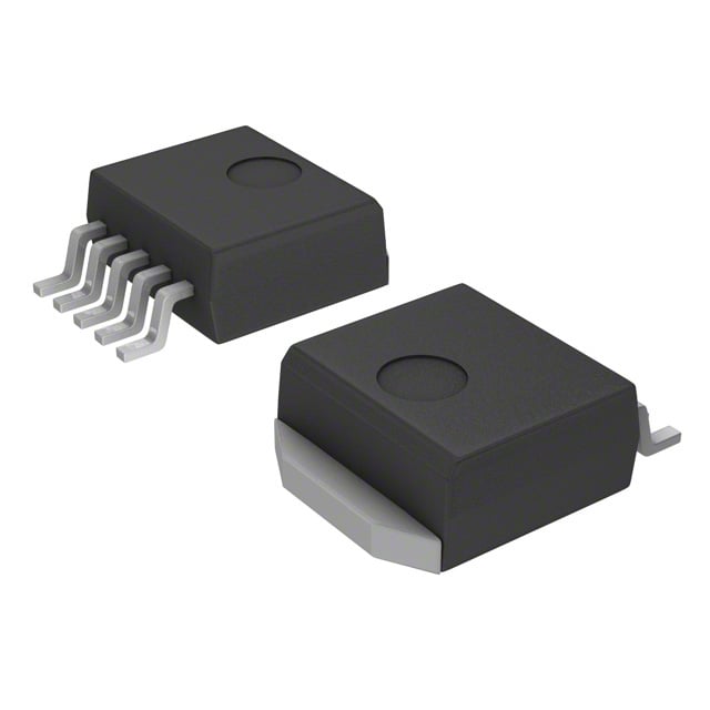
| 供应商器件封装 | D2PAK-5 |
| 其它名称 | LM2931CD2TR4GOSCT |
| 包装 | 剪切带 (CT) |
| 参考电压 | 1.26 V |
| 商标 | ON Semiconductor |
| 回动电压—最大值 | 200 mV at 10 mA |
| 安装类型 | 表面贴装 |
| 安装风格 | SMD/SMT |
| 封装 | Reel |
| 封装/外壳 | TO-263-6,D²Pak(5 引线+接片),TO-263BA |
| 封装/箱体 | TO-263-5 (D2PAK) |
| 工作温度 | -40°C ~ 125°C |
| 工厂包装数量 | 800 |
| 最大工作温度 | + 125 C |
| 最大输入电压 | 40 V |
| 最小工作温度 | - 40 C |
| 最小输入电压 | + 14 V |
| 标准包装 | 1 |
| 电压-跌落(典型值) | 0.16V @ 100mA |
| 电压-输入 | 最高 40 V |
| 电压-输出 | 2.7 V ~ 29.5 V |
| 电压调节准确度 | 5 % |
| 电流-输出 | 100mA |
| 电流-限制(最小值) | - |
| 稳压器拓扑 | 正,可调式 |
| 稳压器数 | 1 |
| 系列 | LM2931 |
| 线路调整率 | 1.5 mV / V |
| 负载调节 | 1 % / V |
| 输出电流 | 100 mA |
| 输出端数量 | 1 Output |
| 输出类型 | Adjustable |


- 商务部:美国ITC正式对集成电路等产品启动337调查
- 曝三星4nm工艺存在良率问题 高通将骁龙8 Gen1或转产台积电
- 太阳诱电将投资9.5亿元在常州建新厂生产MLCC 预计2023年完工
- 英特尔发布欧洲新工厂建设计划 深化IDM 2.0 战略
- 台积电先进制程称霸业界 有大客户加持明年业绩稳了
- 达到5530亿美元!SIA预计今年全球半导体销售额将创下新高
- 英特尔拟将自动驾驶子公司Mobileye上市 估值或超500亿美元
- 三星加码芯片和SET,合并消费电子和移动部门,撤换高东真等 CEO
- 三星电子宣布重大人事变动 还合并消费电子和移动部门
- 海关总署:前11个月进口集成电路产品价值2.52万亿元 增长14.8%


PDF Datasheet 数据手册内容提取
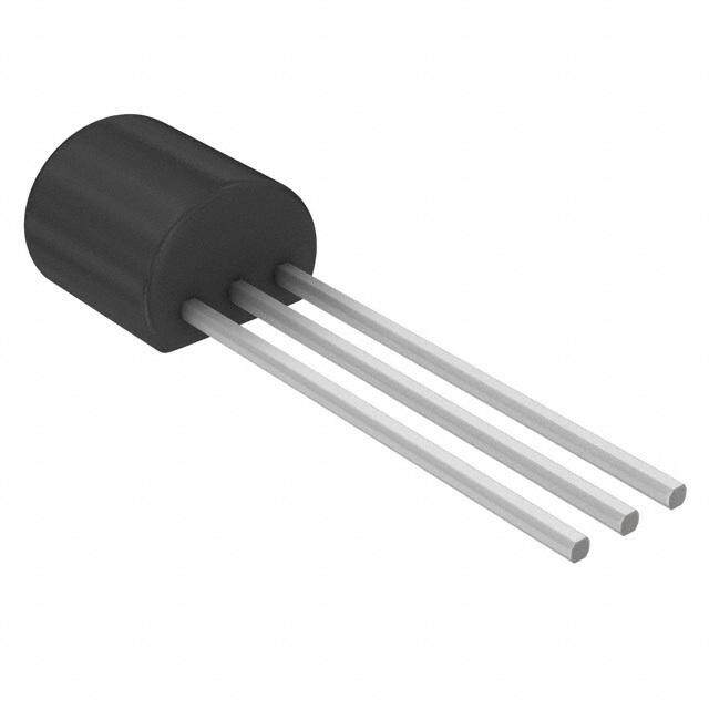
LM2931, NCV2931 Series 100 mA, Adjustable Output, LDO Voltage Regulator with 60 V Load Dump Protection The LM2931 series consists of positive fixed and adjustable output voltage regulators that are specifically designed to maintain proper regulation with an extremely low input−to−output voltage differential. http://onsemi.com These devices are capable of supplying output currents in excess of 100 mA and feature a low bias current of 0.4 mA at 10 mA output. FIXED OUTPUT VOLTAGE Designed primarily to survive in the harsh automotive environment, these devices will protect all external load circuitry from input fault TO−92 Pin 1. Output Z SUFFIX 2. Ground conditions caused by reverse battery connection, two battery jump CASE 29 3. Input starts, and excessive line transients during load dump. This series also 11 2 includes internal current limiting, thermal shutdown, and additionally, 3 is able to withstand temporary power−up with mirror−image insertion. TO−220 T SUFFIX Due to the low dropout voltage and bias current specifications, the CASE 221AB 1 LM2931 series is ideally suited for battery powered industrial and 2 3 consumer equipment where an extension of useful battery life is desirable. The ‘C’ suffix adjustable output regulators feature an output DPAK DT SUFFIX Pin 1. Input inhibit pin which is extremely useful in microprocessor−based systems. 1 CASE 369C 2. Ground 3 Features 3. Output • Input−to−Output Voltage Differential of < 0.6 V @ 100 mA D2PAK • D2T SUFFIX Output Current in Excess of 100 mA CASE 936 1 • 3 Low Bias Current • SOT−223 60 V Load Dump Protection ST SUFFIX • −50 V Reverse Transient Protection CASE 318H 3 1 • Internal Current Limiting with Thermal Shutdown • ADJUSTABLE OUTPUT VOLTAGE Temporary Mirror−Image Protection • Ideally Suited for Battery Powered Equipment TO−220 • TH SUFFIX Economical 5−Lead TO−220 Package with Two Optional Leadforms CASE 314A 11 • Available in Surface Mount SOP−8, D2PAK and DPAK Packages 5 • High Accuracy (±2.5%) Reference (LM2931AC) Available TO−220 1 • NCV Prefix for Automotive and Other Applications Requiring TV SUFFIX Pin 1. Adjust CASE 314B 5 Unique Site and Control Change Requirements; AEC−Q100 2. Output Qualified and PPAP Capable Inhibit • Pb−Free Packages are Available TO−220 3. Ground 4. Input T SUFFIX Applications CASE 314D 1 5. Output • Battery Powered Consumer Products 5 • Hand−held Instruments • D2PAK Camcorders and Cameras D2T SUFFIX 1 SOIC−8 CASE 936A 5 D SUFFIX CASE 751 8 1 ORDERING INFORMATION FIXED ADJUSTABLE See detailed ordering and shipping information in the package Output N.C. 5 4 N.C. Inhibit 5 4 Adjust dimensions section on page 12 of this data sheet. GND GND GND GND Input 8 1 Output Input 8 1 Output DEVICE MARKING INFORMATION See general marking and heatsink information in the device (Top View) (Top View) marking section on page 15 of this data sheet. © Semiconductor Components Industries, LLC, 2013 1 Publication Order Number: April, 2013 − Rev. 26 LM2931/D
LM2931, NCV2931 Series Representative Schematic Diagram Input 6.0 30 k 6.0 k 6.8 V 350 500 Output Inhibit Output 30 k 30 k 50 k 30 k * 48 k 180 k 184 k 5.8 V 3.94 k Adjust EPI 3.0 k Bias 92.8 k * 11.5 k 35 k 10 k Ground *Deleted on Adjustable Regulators This device contains 26 active transistors. http://onsemi.com 2
LM2931, NCV2931 Series MAXIMUM RATINGS Rating Symbol Value Unit Input Voltage Continuous VI 40 Vdc Transient Input Voltage ((cid:2) ≤ 100 ms) VI((cid:2)) 60 Vpk Transient Reverse Polarity Input Voltage −VI((cid:2)) −50− Vpk 1.0% Duty Cycle, (cid:2) ≤ 100 ms Electrostatic Discharge Sensitivity (ESD) Human Body Model (HBM) Class 2, JESD22 A114−C − 2000 V Machine Model (MM) Class A, JESD22 A115−A − 200 V Charged Device Model (CDM), JESD22 C101−C − 2000 V Power Dissipation Case 29 (TO−92 Type) TA = 25°C PD Internally Limited W Thermal Resistance, Junction−to−Ambient R(cid:3)JA 178 °C/W Thermal Resistance, Junction−to−Case R(cid:3)JC 83 °C/W Case 221A, 314A, 314B and 314D (TO−220 Type) TA = 25°C PD Internally Limited W Thermal Resistance, Junction−to−Ambient R(cid:3)JA 65 °C/W Thermal Resistance, Junction−to−Case R(cid:3)JC 5.0 °C/W Case 318H (SOT−223) TA = 25°C PD Internally Limited W Thermal Resistance, Junction−to−Ambient R(cid:3)JA 242 °C/W Thermal Resistance, Junction−to−Case R(cid:3)JC 21 °C/W Case 369A (DPAK) (Note 1) TA = 25°C PD Internally Limited W Thermal Resistance, Junction−to−Ambient R(cid:3)JA 92 °C/W Thermal Resistance, Junction−to−Case R(cid:3)JC 6.0 °C/W Case 751 (SOP−8) (Note 2) TA = 25°C PD Internally Limited W Thermal Resistance, Junction−to−Ambient R(cid:3)JA 160 °C/W Thermal Resistance, Junction−to−Case R(cid:3)JC 25 °C/W Case 936 and 936A (D2PAK) (Note 3) TA = 25°C PD Internally Limited W Thermal Resistance, Junction−to−Ambient R(cid:3)JA 70 °C/W Thermal Resistance, Junction−to−Case R(cid:3)JC 5.0 °C/W Operating Ambient Temperature Range TA −40 to +125 °C Operating Die Junction Temperature TJ +150 °C Storage Temperature Range Tstg −65 to +150 °C Stresses exceeding Maximum Ratings may damage the device. Maximum Ratings are stress ratings only. Functional operation above the Recommended Operating Conditions is not implied. Extended exposure to stresses above the Recommended Operating Conditions may affect device reliability. 1. DPAK Junction−to−Ambient Thermal Resistance is for vertical mounting. Refer to Figure 25 for board mounted Thermal Resistance. 2. SOP−8 Junction−to−Ambient Thermal Resistance is for minimum recommended pad size. Refer to Figure 24 for Thermal Resistance variation versus pad size. 3. D2PAK Junction−to−Ambient Thermal Resistance is for vertical mounting. Refer to Figure 26 for board mounted Thermal Resistance. 4. NCV rated devices are subjected to and meet the AECQ−100 quality standards. http://onsemi.com 3
LM2931, NCV2931 Series ELECTRICAL CHARACTERISTICS (Vin = 14 V, IO = 10 mA, CO = 100 (cid:4)F, CO(ESR) = 0.3 (cid:5), TA = 25°C [Note 5]) LM2931−5.0/NCV2931−5.0 LM2931A−5.0/NCV2931A−5.0 Characteristic Symbol Min Typ Max Min Typ Max Unit FIXED OUTPUT Output Voltage VO V Vin = 14 V, IO = 10 mA, TA = 25°C 4.75 5.0 5.25 4.81 5.0 5.19 Vin = 6.0 V to 26 V, IO ≤ 100 mA, 4.50 − 5.50 4.75 − 5.25 TA = −40° to +125°C Line Regulation Regline mV Vin = 9.0 V to 16 V − 2.0 10 − 2.0 10 Vin = 6.0 V to 26 V − 4.0 30 − 4.0 30 Load Regulation (IO = 5.0 mA to 100 mA) Regload − 14 50 − 14 50 mV Output Impedance ZO m(cid:5) IO = 10 mA, (cid:6)IO = 1.0 mA, f = 100 Hz to − 200 − − 200 − 10 kHz Bias Current IB mA Vin = 14 V, IO = 100 mA, TA = 25°C − 5.8 30 − 5.8 30 Vin = 6.0 V to 26 V, IO = 10 mA, TA = −40° to − 0.4 1.0 − 0.4 1.0 +125°C Output Noise Voltage (f = 10 Hz to 100 kHz) Vn − 700 − − 700 − (cid:4)Vrms Long Term Stability S − 20 − − 20 − mV/kHR Ripple Rejection (f = 120 Hz) RR 60 90 − 60 90 − dB Dropout Voltage VI−VO V IO = 10 mA − 0.015 0.2 − 0.015 0.2 IO = 100 mA − 0.16 0.6 − 0.16 0.6 Over−Voltage Shutdown Threshold Vth(OV) 26 29.5 40 26 29.5 40 V Output Voltage with Reverse Polarity Input −VO −0.3 0 − −0.3 0 − V (Vin = −15 V) 5. Low duty cycle pulse techniques are used during test to maintain junction temperature as close to ambient as possible. 6. NCV devices are qualified for automotive use. http://onsemi.com 4
LM2931, NCV2931 Series ELECTRICAL CHARACTERISTICS (Vin = 14 V, IO = 10 mA, CO = 100 (cid:4)F, CO(ESR) = 0.3 (cid:5), TA = 25°C [Note 7]) LM2931C/NCV2931C LM2931AC/NCV2931AC Characteristic Symbol Min Typ Max Min Typ Max Unit ADJUSTABLE OUTPUT Reference Voltage (Note 8, Figure 18) Vref V IO = 10 mA, TA = 25°C 1.14 1.20 1.26 1.17 1.20 1.23 IO ≤ 100 mA, TA = −40 to +125°C 1.08 − 1.32 1.15 − 1.25 Output Voltage Range VO range 3.0 to 2.7 to − 3.0 to 2.7 to − V 24 29.5 24 29.5 Line Regulation (Vin = VO + 0.6 V to 26 V) Regline − 0.2 1.5 − 0.2 1.5 mV/V Load Regulation (IO = 5.0 mA to 100 mA) Regload − 0.3 1.0 − 0.3 1.0 %/V Output Impedance ZO m(cid:5)(cid:7)V IO = 10 mA, (cid:6)IO = 1.0 mA, f = 10 Hz to 10 kHz − 40 − − 40 − Bias Current IB mA IO = 100 mA − 6.0 − − 6.0 − IO = 10 mA − 0.4 1.0 − 0.4 1.0 Output Inhibited (Vth(OI) = 2.5 V) − 0.2 1.0 − 0.2 1.0 Adjustment Pin Current IAdj − 0.2 − − 0.2 − (cid:4)A Output Noise Voltage (f = 10 Hz to 100 kHz) Vn − 140 − − 140 − (cid:4)Vrms/V Long−Term Stability S − 0.4 − − 0.4 − %/kHR Ripple Rejection (f = 120 Hz) RR 0.10 0.003 − 0.10 0.003 − %/V Dropout Voltage VI−VO V IO = 10 mA − 0.015 0.2 − 0.015 0.2 IO = 100 mA − 0.16 0.6 − 0.16 0.6 Over−Voltage Shutdown Threshold Vth(OV) 26 29.5 40 26 29.5 40 V Output Voltage with Reverse Polarity Input −VO −0.3 0 − −0.3 0 − V (Vin = −15 V) Output Inhibit Threshold Voltages Vth(OI) V Output “On”: TA = 25°C − 2.15 1.90 − 2.15 1.90 TA = −40° to +125°C − − 1.20 − − 1.20 Output “Off”: TA = 25°C 2.50 2.26 − 2.50 2.26 − TA = −40° to +125°C 3.25 − − 3.25 − − Output Inhibit Threshold Current (Vth(OI) = 2.5 V) Ith(OI) − 30 50 − 30 50 (cid:4)A 7. Low duty cycle pulse techniques are used during test to maintain junction temperature as close to ambient as possible. 8. The reference voltage on the adjustable device is measured from the output to the adjust pin across R1. http://onsemi.com 5
LM2931, NCV2931 Series 200 300 TAGE (mV) 160 V(cid:6)TJinV =o= u 2t1 5=4° 1CV00 mV TAGE (mV) 200 V(cid:6)inV o=u t1 =4 1V00 mV IO = 100 mA L L O 120 O V V T T U U O O OP 80 OP R R 100 D D V, O 40 V, O IO = 50 mA - - Vin Vin IO = 10 mA 0 0 0 20 40 60 80 100 0 25 50 75 100 125 IO, OUTPUT CURRENT (mA) TJ, JUNCTION TEMPERATURE (°C) FFiigguurree 11.. DDrrooppoouutt VVoollttaaggee vveerrssuuss OOuuttppuutt CCuurrrreenntt Figure 2. Dropout Voltage versus Junction Temperature 350 6.0 URRENT (mA) 250 TJ = -40°C TJ = 85°C TJ = 25°C OLTAGE (V) 45..00 VTAou =t =2 55°.0C V C V 3.0 T T U U P P UT 150 UT 2.0 O O , IO Daraes fhoer dA ldinjuesst abbelleo wou Vtpinu =t d5e.0v icVes only. , VO 1.0 RL = 50 (cid:5) IO = 100 mA 50 0 0 5.0 10 15 20 25 30 0 1.0 2.0 3.0 4.0 5.0 6.0 Vin, INPUT VOLTAGE (V) Vin, INPUT VOLTAGE (V) Figure 3. Peak Output Current versus Input Voltage Figure 4. Output Voltage versus Input Voltage 6.0 E AG Vout = 5.0 V UT VOLTAGE (V) 345...000 VVCFBC1 = = 1 55. 0V5 V V, INPUT VOLTin(10 V/DIV) RC(cid:2)T ALO= ==1= 5 2510500 ° m0(cid:5)C s(cid:4)F P 0 T U E , OVO12..000 VRTAoLu ==t = 25 505°0.0C (cid:5) V OUTPUT VOLTAG(5.0 V/DIV) 0 -20 -10 0 Vin1,0 INPUT 2V0OLTAG3E0 (V) 40 50 60 V, O t, TIME (50 ms/DIV) Figure 5. Output Voltage versus Input Voltage Figure 6. Load Dump Characteristics http://onsemi.com 6
LM2931, NCV2931 Series 12 8.0 10 Vout = 5.0 V mA) TJ = 25°C mA) 6.0 Vin = 14 V ENT ( 8.0 ENT ( VTJo u=t =2 55°.0C V URR 6.0 RL = 50 (cid:5) URR 4.0 C C S S A A BI 4.0 BI I, B RL = 100 (cid:5) I, B 2.0 2.0 RL = 500 (cid:5) 0 0 -20 -10 0 10 20 30 40 50 60 0 20 40 60 80 100 Vin, INPUT VOLTAGE (V) IO, OUTPUT CURRENT (mA) Figure 7. Bias Current versus Input Voltage Figure 8. Bias Current versus Output Current 8.0 2.0 Vin = 14 V Vin = 14 V mA) 6.0 IO = 100 mA Vout = 5.0 V ΩCE ( (cid:2) ) 1.6 DVIOoI Ou=t ==1 0 15 .m.00 A mVA RENT ( PEDAN 1.2 CTJO = = 2 150°0C (cid:4)F R 4.0 M I, BIAS CUB 2.0 IO = 50 mA , OUTPUT IO 00..48 COE(EleScRt)r o=l y0t.i3c (cid:5) CO(ETSaRn)t u=l u0m.15 (cid:5) I IO = 0 mA 0 0 -55 -25 0 25 50 75 100 125 10 100 1.0 k 10 k 100 k 1.0 M 10 M TJ, JUNCTION TEMPERATURE (°C) f, FREQUENCY (Hz) Figure 9. Bias Current versus Junction Temperature Figure 10. Output Impedance versus Frequency 95 95 O (dB) O (dB) RR, RIPPLE REJECTION RATI 678555 VDRCTVJoiVLOn u = i=tn== = 2 =511 5 05401°0. 000CV 0(cid:5) (cid:4)V mFV COE(EleScRt)r o=l y0t.i3c (cid:5) CO(ETSaRn)t u=l u0m.15 (cid:5) RR, RIPPLE REJECTION RATI 8755 VVfT =Join u =1t= 2= 210 554 °H. 0CVz V 55 65 10 100 1.0 k 10 k 100 k 1.0 M 10 M 0 20 40 60 80 100 f, FREQUENCY (Hz) IO, OUTPUT CURRENT (mA) Figure 11. Ripple Rejection versus Frequency Figure 12. Ripple Rejection versus Output Current http://onsemi.com 7
LM2931, NCV2931 Series N, N, O O TI TI A A VIV) VIV) UT VOLTAGE DEΔ, (2.0 mV/DIVO18.5 CVRoLOu =t= = 51 0500.00 (cid:5) (cid:4)VF UT VOLTAGE DEΔ, (2.0 mV/DIVO VCVoiinnu t== = 11 540. 00V0 V (cid:4)F OUTP CTAO (=E S2R5)° C= 0.3 (cid:5) OUTP 100 CCOO (E=S 1R0) 0= (cid:4)0F.3 (cid:5) T, TA = 25°C N E, 14 E 0 AG RRA) PUT VOLTV , (V)in Figuret , 1T3IM. EL (i1n0e (cid:4) sR/DeIVg)ulation UTPUT CUI (mout Figure t,1 T4IM. EL (o1a0 d(cid:4)s R/DeIVg)ulation N O I 1.240 V) 2.6 LM2931C Adjustable S ( LM2931C Adjustable OLTAGE (V)1.220 IVTOAin = == 1 2V05o °muCt A+ 1.0 V THRESHOLD 22..45 IVTOAin = == 1 2V05o °muCt A+ 1.0 V Output “Off" NCE V1.200 HIBIT‐ 2.3 E N EFER PUT I 2.2 , RVref1.180 , OUT 2.1 Output “On" off) n/ 1.1600 3.0 6.0 9.0 12 15 18 21 24 Vth(o 2.00 3.0 6.0 9.0 12 15 18 21 24 VO, OUTPUT VOLTAGE (V) VO, OUTPUT VOLTAGE (V) Figure 15. Reference Voltage versus Output Voltage Figure 16. Output Inhibit−Thresholds versus Output Voltage APPLICATIONS INFORMATION The LM2931 series regulators are designed with many limit must be observed over the entire operating temperature protection features making them essentially blow−out range of the regulator circuit. proof. These features include internal current limiting, With economical electrolytic capacitors, cold temperature thermal shutdown, overvoltage and reverse polarity input operation can pose a serious stability problem. As the protection, and the capability to withstand temporary electrolyte freezes, around −30°C, the capacitance will power−up with mirror−image insertion. Typical application decrease and the equivalent series resistance (ESR) will circuits for the fixed and adjustable output device are shown increase drastically, causing the circuit to oscillate. Quality in Figures 17 and 18. electrolytic capacitors with extended temperature ranges of The input bypass capacitor C is recommended if the −40° to +85°C and −55° to +105°C are readily available. in regulator is located an appreciable distance (≥ 4″) from the Solid tantalum capacitors may be a better choice if small size supply input filter. This will reduce the circuit’s sensitivity is a requirement, however, the maximum ⏐Z ⏐ limit over O to the input line impedance at high frequencies. temperature must be observed. This regulator series is not internally compensated and Note that in the stable region, the output noise voltage is thus requires an external output capacitor for stability. The linearly proportional to ⏐Z ⏐ In effect, C dictates the high O . O capacitance value required is dependent upon the load frequency roll−off point of the circuit. Operation in the area current, output voltage for the adjustable regulator, and the titled “Marginally Stable” will cause the output of the type of capacitor selected. The least stable condition is regulator to exhibit random bursts of oscillation that decay encountered at maximum load current and minimum output in an under−damped fashion. Continuous oscillation occurs voltage. Figure 22 shows that for operation in the “Stable” when operating in the area titled “Unstable”. It is suggested region, under the conditions specified, the magnitude of the that oven testing of the entire circuit be performed with output capacitor impedance |Z | must not exceed 0.4 (cid:5). This maximum load, minimum input voltage, and minimum O ambient temperature. http://onsemi.com 8
LM2931, NCV2931 Series Input Output Vin Vout LM2931C 51 k Output Adjustable R1 2 Inhibit Output Adjust 0C.i1n CO 1 IAdj IB GND R2 Input LM2931-5.0 Output Vin Fixed Vout Output 0C.i1n IB GND CO Vout(cid:2)(cid:4)(cid:2)SVwrietcf(cid:2)h(cid:5) P1o(cid:2)s(cid:3)itio(cid:2)nRR 121 (cid:6)= (cid:2)O(cid:3)utp(cid:2)uIAt d“Oj(cid:2)Rn"2, 2 = O2u2t.p5u(cid:2)kt(cid:2) “(cid:2)Off(cid:2)"R1R(cid:2)1(cid:3)(cid:2)R(cid:2)2R2 Figure 17. Fixed Output Regulator Figure 18. Adjustable Output Regulator RSC D45VH7 Input Input ≥ 6.0 V R 68 R Output 5.0 V @ 5.0 A LM2931-5.0 LM2931-5.0 + + Output + + 100 100 100 100 The LM2931 series can be current boosted with a PNP transistor. The The circuit of Figure 19 can be modified to provide supply protection against D45VH7, on a heatsink, will provide an output current of 5.0 A with an input short circuits by adding the current sense resistor RSC and an additional PNP to output voltage differential of approximately 1.0 V. Resistor R in transistor. The current sensing PNP must be capable of handling the short conjunction with the VBE of the PNP determines when the pass transistor circuit current of the LM2931. Safe operating area of both transistors must be begins conducting. This circuit is not short circuit proof. considered under worst case conditions. Figure 19. (5.0 A) Low Differential Figure 20. Current Boost Regulator with Voltage Regulator Short Circuit Projection Input 6.4 V to 30 V LM2931C 2.0 k + 100 8.2 k CM #345 + 33 k 100 6.2 V 0 fosc = 2.2 Hz Figure 21. Constant Intensity Lamp Flasher http://onsemi.com 9
LM2931, NCV2931 Series 100 0.60 ms) Vin = 5.6 V 10 (cid:4)F SE VOLTAGE (mVr 11.00 VIV|TZOAonO u r==m|t =@12s0 551 04°.0 0C0m H VkAzH tzo 10 MHz UMStnaasrbgtalienbalelly Ohms) 000...345000 1240270 (cid:4)(cid:4) (cid:4)FFF Unstable NOI SR ( Stable UT E 0.20 P T 0.1 U Note - Optimum stability uses a 22 (cid:4)F V, On Stable 0.10 obeultopwut 1c0a p(cid:4)aFc iatorer. nOout trpeucto cmapmaecnitdoer dv.alues 0.01 0.00 10 100 1.0 k 10 k 0 10 20 30 40 50 60 70 80 90 100 |ZO|, MAGNITUDE OF CAPACITOR IMPEDANCE (m(cid:5)) OUTPUT CURRENT (mA) Figure 22. Output Noise Voltage vs. Figure 23. Output Capacitor ESR Stability vs. Output Capacitor Impedance Output Load Current 170 3.2 W) , THERMAL RESISTANCEθJA°JUNCTION-TO-AIR ( C/W) 1117913500000 GLraÎÎphC2 r.o0epPL pÎÎopDrzee(.mrseaÎÎÎÎnx)t sfo sry ÎÎTmAm =e ÎÎÎÎ5tr0ic°aC3l ÎÎl.a0y moumÎÎt 11222.....26048 XIMUM POWER DISSIPATION ( R 50 0.8 MA R(cid:3)JA , D 30 0.4 P 0 10 20 30 40 50 L, LENGTH OF COPPER (mm) Figure 24. SOP−8 Thermal Resistance and Maximum Power Dissipation versus P.C.B. Copper Length 100 2.4 NCE W) 90 MFroeuen Ateidr PD(max) for TA = 50°C 2.0 ON (W) RMAL RESISTA°N-TO-AIR ( C/ 7800 VerticalMSlyiizneim Puamd ÎÎÎL2.0 oÎÎÎz. CLoÎÎÎpperÎÎÎ11..26 WER DISSIPATI E O O , THANCTI 60 ÎÎÎÎ0.8 UM P JU M Rθ J 50 0.4 AXI R(cid:3)JA , MD 40 0 P 0 5.0 10 15 20 25 30 L, LENGTH OF COPPER (mm) Figure 25. DPAK Thermal Resistance and Maximum Power Dissipation versus P.C.B. Copper Length http://onsemi.com 10
LM2931, NCV2931 Series 80 3.5 RMAL RESISTANCE°N-TO-AIR ( C/W) 6700 VMFeroreuteicn aAtelildry MinimumPD(max) for TA = 5ÎÎ20.°0C oÎÎz. CLoÎÎpperÎÎ23..50 WER DISSIPATION (W) , THEANCTIO 50 Size Pad LÎÎÎÎ2.0 UM PO RθJJU 40 ÎÎÎÎ1.5 XIM A R(cid:3)JA , MD 30 1.0 P 0 5.0 10 15 20 25 30 L, LENGTH OF COPPER (mm) Figure 26. 3−Pin and 5−Pin D2PAK Thermal Resistance and Maximum Power Dissipation versus P.C.B. Copper Length W) 300 1.8 E, PD(max) for TA = 50°C 1.6 ON ( ANCCW) 250 1.4 PATI ESIST°AIR ( 200 2.Î0 oz.Î CLopÎper 1.2 DISSI AL R−TO− 150 LÎÎÎ 10..08 WER MN O R, THER(cid:3)JAJUNCTIO 15000 R(cid:3)JA ÎÎÎ 000...642 AXIMUM P M 0 0.0 , D 0 5.0 10 15 20 25 30 P L, LENGTH OF COPPER (mm) Figure 27. SOT−223 Thermal Resistance and Maximum Power Dissipation vs. P.C.B. Copper Length DEFINITIONS Dropout Voltage − The input/output voltage differential Maximum Power Dissipation − The maximum total at which the regulator output no longer maintains regulation device dissipation for which the regulator will operate against further reductions in input voltage. Measured when within specifications. the output decreases 100 mV from nominal value at 14 V Bias Current − That part of the input current that is not input, dropout voltage is affected by junction temperature delivered to the load. and load current. Output Noise Voltage − The rms AC voltage at the Line Regulation − The change in output voltage for a output, with constant load and no input ripple, measured change in the input voltage. The measurement is made under over a specified frequency range. conditions of low dissipation or by using pulse techniques Long−Term Stability − Output voltage stability under such that the average chip temperature is not significantly accelerated life test conditions with the maximum rated affected. voltage listed in the devices electrical characteristics and Load Regulation − The change in output voltage for a maximum power dissipation. change in load current at constant chip temperature. http://onsemi.com 11
LM2931, NCV2931 Series ORDERING INFORMATION Output Device Voltage Tolerance Package Shipping† LM2931AD−5.0 5.0 V (cid:7)3.8% SOIC−8 98 Units / Rail LM2931AD−5.0G 5.0 V (cid:7)3.8% SOIC−8 98 Units / Rail (Pb−Free) LM2931AD−5.0R2 5.0 V (cid:7)3.8% SOIC−8 2500 / Tape & Reel LM2931AD−5.0R2G 5.0 V (cid:7)3.8% SOIC−8 2500 / Tape & Reel (Pb−Free) LM2931ADT−5.0 5.0 V (cid:7)3.8% DPAK 75 Units / Rail LM2931ADT−5.0G 5.0 V (cid:7)3.8% DPAK 75 Units / Rail (Pb−Free) LM2931ADT−5.0RK 5.0 V (cid:7)3.8% DPAK 2500 / VacPk Reel LM2931ADT−5.0RKG 5.0 V (cid:7)3.8% DPAK 2500 / VacPk Reel (Pb−Free) LM2931AD2T−5.0 5.0 V (cid:7)3.8% D2PAK 50 Units / Rail LM2931AD2T−5.0G 5.0 V (cid:7)3.8% D2PAK 50 Units / Rail (Pb−Free) LM2931AD2T−5.0R4 5.0 V (cid:7)3.8% D2PAK 800 / VacPk Reel LM2931AD2T−5R4G 5.0 V (cid:7)3.8% D2PAK 800 / VacPk Reel (Pb−Free) LM2931AT−5.0 5.0 V (cid:7)3.8% TO−220 50 Units / Rail LM2931AT−5.0G 5.0 V (cid:7)3.8% TO−220 50 Units / Rail (Pb−Free) LM2931AZ−5.0 5.0 V (cid:7)3.8% TO−92 2000 / Inner Bag LM2931AZ−5.0G 5.0 V (cid:7)3.8% TO−92 2000 / Inner Bag (Pb−Free) LM2931AZ−5.0RA 5.0 V (cid:7)3.8% TO−92 2000 / Tape & Reel LM2931AZ−5.0RAG 5.0 V (cid:7)3.8% TO−92 2000 / Tape & Reel (Pb−Free) LM2931AZ−5.0RP 5.0 V (cid:7)3.8% TO−92 2000 / Ammo Pack LM2931AZ−5.0RPG 5.0 V (cid:7)3.8% TO−92 2000 / Ammo Pack (Pb−Free) LM2931D−5.0 5.0 V (cid:7)5.0% SOIC−8 98 Units / Rail LM2931D−5.0G 5.0 V (cid:7)5.0% SOIC−8 98 Units / Rail (Pb−Free) LM2931D−5.0R2 5.0 V (cid:7)5.0% SOIC−8 2500 / Tape & Reel LM2931D−5.0R2G 5.0 V (cid:7)5.0% SOIC−8 2500 / Tape & Reel (Pb−Free) LM2931D2T−5.0 5.0 V (cid:7)5.0% D2PAK 50 Units / Rail LM2931D2T−5.0G 5.0 V (cid:7)5.0% D2PAK 50 Units / Rail (Pb−Free) LM2931D2T−5.0R4 5.0 V (cid:7)5.0% D2PAK 800 / VacPk Reel LM2931D2T−5.0R4G 5.0 V (cid:7)5.0% D2PAK 800 / VacPk Reel (Pb−Free) †For information on tape and reel specifications, including part orientation and tape sizes, please refer to our Tape and Reel Packaging Spe- cifications Brochure, BRD8011/D. *NCV2931: Tlow = −40°C, Thigh = +125°C. Guaranteed by design. NCV Prefix for Automotive and Other Applications Requiring Unique Site and Control Change Requirements; AEC−Q100 Qualified and PPAP Capable. http://onsemi.com 12
LM2931, NCV2931 Series ORDERING INFORMATION Output DDeevviiccee Voltage Tolerance PPaacckkaaggee SShhiippppiinngg†† LM2931DT−5.0 5.0 V (cid:7)5.0% DPAK 75 Units / Rail LM2931DT−5.0G 5.0 V (cid:7)5.0% DPAK 75 Units / Rail (Pb−Free) LM2931T−5.0 5.0 V (cid:7)5.0% TO−220 50 Units / Rail LM2931T−5.0G 5.0 V (cid:7)5.0% TO−220 50 Units / Rail (Pb−Free) LM2931Z−5.0 5.0 V (cid:7)5.0% TO−92 2000 / Inner Bag LM2931Z−5.0G 5.0 V (cid:7)5.0% TO−92 2000 / Inner Bag (Pb−Free) LM2931Z−5.0RA 5.0 V (cid:7)5.0% TO−92 2000 / Tape & Reel LM2931Z−5.0RAG 5.0 V (cid:7)5.0% TO−92 2000 / Tape & Reel (Pb−Free) LM2931Z−5.0RP 5.0 V (cid:7)5.0% TO−92 2000 / Ammo Pack LM2931Z−5.0RPG 5.0 V (cid:7)5.0% TO−92 2000 / Ammo Pack (Pb−Free) LM2931CD Adjustable (cid:7)5.0% SOIC−8 98 Units / Rail LM2931CDG Adjustable (cid:7)5.0% SOIC−8 98 Units / Rail (Pb−Free) LM2931CDR2 Adjustable (cid:7)5.0% SOIC−8 2500 / Tape & Reel LM2931CDR2G Adjustable (cid:7)5.0% SOIC−8 2500 / Tape & Reel (Pb−Free) LM2931CD2T Adjustable (cid:7)5.0% D2PAK 50 Units / Rail LM2931CD2TG Adjustable (cid:7)5.0% D2PAK 50 Units / Rail (Pb−Free) LM2931CD2TR4 Adjustable (cid:7)5.0% D2PAK 800 / VacPk Reel LM2931CD2TR4G Adjustable (cid:7)5.0% D2PAK 800 / VacPk Reel (Pb−Free) LM2931CT Adjustable (cid:7)5.0% TO−220 50 Units / Rail LM2931CTG Adjustable (cid:7)5.0% TO−220 50 Units / Rail (Pb−Free) LM2931ACD Adjustable (cid:7)2.0% SOIC−8 98 Units / Rail LM2931ACDG Adjustable (cid:7)2.0% SOIC−8 98 Units / Rail (Pb−Free) LM2931ACDR2 Adjustable (cid:7)2.0% SOIC−8 2500 / Tape & Reel LM2931ACDR2G Adjustable (cid:7)2.0% SOIC−8 2500 / Tape & Reel (Pb−Free) LM2931ACD2TR4 Adjustable (cid:7)2.0% D2PAK 800 / VacPk Reel LM2931ACD2TR4G Adjustable (cid:7)2.0% D2PAK 800 / VacPk Reel (Pb−Free) LM2931ACTV Adjustable (cid:7)2.0% TO−220 50 Units / Rail LM2931ACTVG Adjustable (cid:7)2.0% TO−220 50 Units / Rail (Pb−Free) †For information on tape and reel specifications, including part orientation and tape sizes, please refer to our Tape and Reel Packaging Spe- cifications Brochure, BRD8011/D. *NCV2931: Tlow = −40°C, Thigh = +125°C. Guaranteed by design. NCV Prefix for Automotive and Other Applications Requiring Unique Site and Control Change Requirements; AEC−Q100 Qualified and PPAP Capable. http://onsemi.com 13
LM2931, NCV2931 Series ORDERING INFORMATION Output DDeevviiccee Voltage Tolerance PPaacckkaaggee SShhiippppiinngg†† NCV2931ACDR2* Adjustable (cid:7)2.5% SOIC−8 2500 / Tape & Reel NCV2931ACDR2G* Adjustable (cid:7)2.5% SOIC−8 2500 / Tape & Reel (Pb−Free) NCV2931AD−5.0R2* 5.0 V (cid:7)3.8% SOIC−8 2500 / Tape & Reel NCV2931AD−5.0R2G* 5.0 V (cid:7)3.8% SOIC−8 2500 / Tape & Reel (Pb−Free) NCV2931AST−5.0T3* 5.0 V (cid:7)3.8% SOT−223 4000 / Tape & Reel NCV2931AST−5.0T3G* 5.0 V (cid:7)3.8% SOT−223 4000 / Tape & Reel (Pb−Free) NCV2931AZ−5.0G* 5.0 V (cid:7)3.8% TO−92 2000 / Inner Bag (Pb−Free) NCV2931AZ−5.0RAG* 5.0 V (cid:7)3.8% TO−92 2000 / Tape & Reel (Pb−Free) NCV2931CDR2* Adjustable (cid:7)5.0% SOIC−8 2500 / Tape & Reel NCV2931CDR2G* Adjustable (cid:7)5.0% SOIC−8 2500 / Tape & Reel (Pb−Free) NCV2931D−5.0R2* 5.0 V (cid:7)5.0% SOIC−8 2500 / Tape & Reel NCV2931D−5.0R2G* 5.0 V (cid:7)5.0% SOIC−8 2500 / Tape & Reel (Pb−Free) NCV2931ADT−5.0RK* 5.0 V (cid:7)3.8% DPAK 2500 / Tape & Reel NCV2931ADT5.0RKG* 5.0 V (cid:7)3.8% DPAK 2500 / Tape & Reel (Pb−Free) NCV2931DT−5.0RK* 5.0 V (cid:7)5.0% DPAK 2500 / Tape & Reel NCV2931DT−5.0RKG* 5.0 V (cid:7)5.0% DPAK 2500 / Tape & Reel (Pb−Free) NCV2931ACD2TR4G* Adjustable (cid:7)2.5% D2PAK 800 / VacPk Reel (Pb−Free) NCV2931D2T−5.0R4* 5.0 V (cid:7)5.0% D2PAK 800 / VacPk Reel NCV2931D2T5.0R4G* 5.0 V (cid:7)5.0% D2PAK 800 / VacPk Reel (Pb−Free) †For information on tape and reel specifications, including part orientation and tape sizes, please refer to our Tape and Reel Packaging Spe- cifications Brochure, BRD8011/D. *NCV2931: Tlow = −40°C, Thigh = +125°C. Guaranteed by design. NCV Prefix for Automotive and Other Applications Requiring Unique Site and Control Change Requirements; AEC−Q100 Qualified and PPAP Capable. http://onsemi.com 14
LM2931, NCV2931 Series MARKING DIAGRAMS DPAK DPAK D2PAK D2PAK D2PAK DT SUFFIX DT SUFFIX D2T SUFFIX D2T SUFFIX D2T SUFFIX CASE 369A CASE 369A CASE 936 CASE 936 CASE 936 * * 931A5G 2931G LM LM LM ALYWW AALLYYWWWW 2931AD2T−5 2931AD2T−5.0 2931D2T−5 AWLYWWG AWLYWWG AWLYWWG Heatsink surface (shown as terminal 4 in case outline drawing) is connected to Pin 2. TO−220 TO−220 TO−220 D2PAK D2PAK T SUFFIX T SUFFIX T SUFFIX D2T SUFFIX D2T SUFFIX CASE 221A CASE 221A CASE 314D CASE 936A CASE 936A LM LM LM LM LM 2931ACD2T 2931CT 2931AT−5 2931T−5.0 2931ACTV AWLYWWG AWLYWWG AWLYWWG AWLYWWG AWLYWWG Heatsink surface connected to Pin 2. Heatsink surface Heatsink surface (shown as terminal 6 in connected to Pin 3. case outline drawing) is connected to Pin 3. SOIC−8 SOIC−8 SOIC−8 SOIC−8 TO−92 TO−92 D SUFFIX D SUFFIX D SUFFIX D SUFFIX Z SUFFIX Z SUFFIX CASE 751 CASE 751 CASE 751 CASE 751 CASE 029 CASE 029 8 8 8 8 2931A 2931Z 2931A 2931A * 2931C * 2931 Z−5.0 −5.0 ALYW ALYW5 ALYW ALYW5 ALYW(cid:2) ALYW(cid:2) (cid:2) (cid:2) (cid:2) (cid:2) (cid:2) (cid:2) 1 1 1 1 SOT−223 ST SUFFIX CASE 318H * A = Assembly Location ALYW WL, L = Wafer Lot 2931A(cid:2) YY, Y = Year (cid:2) WW, W = Work Week G or (cid:2) = Pb−Free Device 1 2 3 *This marking diagram also applies to NCV2931. http://onsemi.com 15
LM2931, NCV2931 Series PACKAGE DIMENSIONS TO−92 (TO−226) CASE 29−11 ISSUE AM 1 12 2 3 3 STRAIGHT LEAD BENT LEAD BULK PACK TAPE & REEL AMMO PACK A NOTES: B STRAIGHT LEAD 1. DIMENSIONING AND TOLERANCING PER ANSI BULK PACK Y14.5M, 1982. 2. CONTROLLING DIMENSION: INCH. R 3. CONTOUR OF PACKAGE BEYOND DIMENSION R IS UNCONTROLLED. 4. LEAD DIMENSION IS UNCONTROLLED IN P AND P BEYOND DIMENSION K MINIMUM. L SEATING INCHES MILLIMETERS PLANE K DIM MIN MAX MIN MAX A 0.175 0.205 4.45 5.20 B 0.170 0.210 4.32 5.33 C 0.125 0.165 3.18 4.19 D 0.016 0.021 0.407 0.533 X X D G 0.045 0.055 1.15 1.39 G H 0.095 0.105 2.42 2.66 J 0.015 0.020 0.39 0.50 H J K 0.500 --- 12.70 --- L 0.250 --- 6.35 --- V C N 0.080 0.105 2.04 2.66 P --- 0.100 --- 2.54 SECTION X−X R 0.115 --- 2.93 --- 1 N V 0.135 --- 3.43 --- N R A B BENT LEAD N1O.TEDSIM:ENSIONING AND TOLERANCING PER TAPE & REEL ASME Y14.5M, 1994. 2. CONTROLLING DIMENSION: MILLIMETERS. AMMO PACK 3. CONTOUR OF PACKAGE BEYOND DIMENSION R IS UNCONTROLLED. 4. LEAD DIMENSION IS UNCONTROLLED IN P P AND BEYOND DIMENSION K MINIMUM. T MILLIMETERS SPELAATNIENG K DIM MIN MAX A 4.45 5.20 B 4.32 5.33 C 3.18 4.19 D 0.40 0.54 X X D G 2.40 2.80 G J 0.39 0.50 K 12.70 --- J N 2.04 2.66 V P 1.50 4.00 C R 2.93 --- V 3.43 --- SECTION X−X 1 N http://onsemi.com 16
LM2931, NCV2931 Series PACKAGE DIMENSIONS TO−220, SINGLE GAUGE CASE 221AB−01 ISSUE A NOTES: 1. DIMENSIONING AND TOLERANCING PER ANSI Y14.5M, 1982. −T− SPELAATNIENG 23.. CDOIMNETNRSOIOLLNI NZG D DEFIMINEENSS IAO ZNO: INNEC WHEHSE.RE ALL BODY AND B F C LEAD IRREGULARITIES ARE ALLOWED. 4. PRODUCT SHIPPED PRIOR TO 2008 HAD DIMENSIONS T S S = 0.045 - 0.055 INCHES (1.143 - 1.397 MM) 4 INCHES MILLIMETERS DIM MIN MAX MIN MAX A 0.570 0.620 14.48 15.75 Q A B 0.380 0.405 9.66 10.28 C 0.160 0.190 4.07 4.82 1 2 3 U D 0.025 0.035 0.64 0.88 H F 0.142 0.147 3.61 3.73 G 0.095 0.105 2.42 2.66 K H 0.110 0.155 2.80 3.93 Z J 0.018 0.025 0.46 0.64 K 0.500 0.562 12.70 14.27 L 0.045 0.060 1.15 1.52 N 0.190 0.210 4.83 5.33 L R Q 0.100 0.120 2.54 3.04 R 0.080 0.110 2.04 2.79 V J S 0.020 0.024 0.508 0.61 G T 0.235 0.255 5.97 6.47 U 0.000 0.050 0.00 1.27 D V 0.045 --- 1.15 --- N Z --- 0.080 --- 2.04 http://onsemi.com 17
LM2931, NCV2931 Series PACKAGE DIMENSIONS TO−220 TH SUFFIX CASE 314A−03 ISSUE E B −T− SPELAATNIENG NO1T.EDSI:MENSIONING AND TOLERANCING PER ANSI −P− Y14.5M, 1982. Q 2.CONTROLLING DIMENSION: INCH. C 3.DIMENSION D DOES NOT INCLUDE INTERCONNECT BAR (DAMBAR) PROTRUSION. E DIMENSION D INCLUDING PROTRUSION SHALL OPTIONAL NOT EXCEED 0.043 (1.092) MAXIMUM. CHAMFER A U INCHES MILLIMETERS DIM MIN MAX MIN MAX A 0.572 0.613 14.529 15.570 F L K B 0.390 0.415 9.906 10.541 C 0.170 0.180 4.318 4.572 D 0.025 0.038 0.635 0.965 E 0.048 0.055 1.219 1.397 G F 0.570 0.585 14.478 14.859 G 0.067 BSC 1.702 BSC 5XD J 0.015 0.025 0.381 0.635 5X J K 0.730 0.745 18.542 18.923 0.014 (0.356) M T P M L 0.320 0.365 8.128 9.271 S Q 0.140 0.153 3.556 3.886 S 0.210 0.260 5.334 6.604 U 0.468 0.505 11.888 12.827 TO−220 TV SUFFIX CASE 314B−05 ISSUE L NOTES: B C 1. DIMENSIONING AND TOLERANCING PER ANSI Q −P− OCHPATIMOFNEARL E 2. YC1O4N.5TMR,O 1L9L8I2N.G DIMENSION: INCH. 3. DIMENSION D DOES NOT INCLUDE INTERCONNECT BAR (DAMBAR) PROTRUSION. DIMENSION D INCLUDING PROTRUSION SHALL NOT EXCEED 0.043 (1.092) MAXIMUM. A U INCHES MILLIMETERS S L DIM MIN MAX MIN MAX W V A 0.572 0.613 14.529 15.570 F B 0.390 0.415 9.906 10.541 K C 0.170 0.180 4.318 4.572 D 0.025 0.038 0.635 0.965 E 0.048 0.055 1.219 1.397 F 0.850 0.935 21.590 23.749 G 0.067 BSC 1.702 BSC H 0.166 BSC 4.216 BSC J 0.015 0.025 0.381 0.635 5X J K 0.900 1.100 22.860 27.940 G 0.24 (0.610) M T H NL 0.302.3020 B0S.C365 8.182.1828 B9S.C271 5X D Q 0.140 0.153 3.556 3.886 0.10 (0.254) M T P M N US 0.4-6-8- 00..652005 11.-8-8-8 1152..784287 V --- 0.735 --- 18.669 −T− SPELAATNIENG W 0.090 0.110 2.286 2.794 http://onsemi.com 18
LM2931, NCV2931 Series PACKAGE DIMENSIONS TO−220 5−LEAD CASE 314D−04 ISSUE H −T− SPELAATNIENG NOTES: B 1.DIMENSIONING AND TOLERANCING PER ANSI −Q− B1 DETAIL A-A E C 2.YC1O4N.5TMR,O 1L9L8I2N.G DIMENSION: INCH. 3.DIMENSION D DOES NOT INCLUDE INTERCONNECT BAR (DAMBAR) PROTRUSION. DIMENSION D INCLUDING PROTRUSION SHALL NOT EXCEED 10.92 (0.043) MAXIMUM. U A L INCHES MILLIMETERS DIM MIN MAX MIN MAX 12345 K A 0.572 0.613 14.529 15.570 B 0.390 0.415 9.906 10.541 B1 0.375 0.415 9.525 10.541 C 0.170 0.180 4.318 4.572 D 0.025 0.038 0.635 0.965 E 0.048 0.055 1.219 1.397 J G 0.067 BSC 1.702 BSC G H H 0.087 0.112 2.210 2.845 J 0.015 0.025 0.381 0.635 D 5 PL K 0.977 1.045 24.810 26.543 0.356 (0.014) M T Q M L 0.320 0.365 8.128 9.271 Q 0.140 0.153 3.556 3.886 B U 0.105 0.117 2.667 2.972 B1 DETAIL A−A SOT−223 ST SUFFIX CASE 318H−01 ISSUE O H E 0.08 NOTES: 1. DIMENSIONS ARE IN MILLIMETERS. 2. INTERPRET DIMENSIONS AND TOLERANCES 0.2 M C B S PER ASME Y14.5M, 1994. C 3. DIMENSION E1 DOES NOT INCLUDE INTERLEAD FLASH OR PROTRUSION. INTERLEAD FLASH OR B S PROTRUSION SHALL NOT EXCEED 0.23 PER 3 B SIDE. 4. DIMENSIONS b AND b2 DO NOT INCLUDE A e S DAMBAR PROTRUSION. ALLOWABLE DAMBAR D e1 A PROTRUSION SHALL BE 0.08 TOTAL IN EXCESS 2 C OF THE b AND b2 DIMENSIONS AT MAXIMUM b MATERIAL CONDITION. A 4 M 5. TREERFMERINEANLC NEU OMNBLEYR.S ARE SHOWN FOR b2 B 1 0.1 6. DIMENSIONS D AND E1 ARE TO BE DETERMINED AT DATUM PLANE H. 0.1 M C A S B S E1 MILLIMETERS A B A1 DIM MIN MAX A A --- 1.80 A1 0.02 0.11 b 0.60 0.88 b1 0.60 0.80 (b2) (b) b2 2.90 3.10 ÉÉÉÉÉÉÉ ÉÉÉ b3 2.90 3.05 c 0.24 0.35 ÉÇÉÇÉÇÉÇÉÇÉÇÉÇ (cid:8) c1ÉÇÉÇÉÇc c1 0.24 0.30 D 6.30 6.70 E 6.70 7.30 b1 E1 3.30 3.70 b3 e 2.30 e1 4.60 SECTION B−B L SECTION A−A (cid:8)L 0.02 5(cid:3) 1--0- (cid:3) http://onsemi.com 19
LM2931, NCV2931 Series PACKAGE DIMENSIONS DPAK DT SUFFIX CASE 369C−01 ISSUE D NOTES: C 1.DIMENSIONING AND TOLERANCING PER ASME A Y14.5M, 1994. E A 2.CONTROLLING DIMENSION: INCHES. 3.THERMAL PAD CONTOUR OPTIONAL WITHIN DI- MENSIONS b3, L3 and Z. b3 B c2 4.DIMENSIONS D AND E DO NOT INCLUDE MOLD FLASH, PROTRUSIONS, OR BURRS. MOLD FLASH, PROTRUSIONS, OR GATE BURRS SHALL NOT EXCEED 0.006 INCHES PER SIDE. L3 4 Z 5.DOIUMTEENRSMIOONSST DE XATNRDE ME EASR EO FD ETTHEER PMLIANSETDIC A TB OTHDEY. D H 6.DATUMS A AND B ARE DETERMINED AT DATUM 1 2 3 DETAIL A PLANE H. INCHES MILLIMETERS DIM MIN MAX MIN MAX L4 A 0.086 0.094 2.18 2.38 b2 A1 0.000 0.005 0.00 0.13 b c b 0.025 0.035 0.63 0.89 b2 0.030 0.045 0.76 1.14 e 0.005 (0.13) M C H b3 0.180 0.215 4.57 5.46 c 0.018 0.024 0.46 0.61 L2 GPLAAUNGEE C SPELAATNIENG cD2 00..203158 00..204254 50..9476 06..6212 E 0.250 0.265 6.35 6.73 e 0.090 BSC 2.29 BSC H 0.370 0.410 9.40 10.41 L A1 L 0.055 0.070 1.40 1.78 L1 L1 0.108 REF 2.74 REF L2 0.020 BSC 0.51 BSC DETAIL A L3 0.035 0.050 0.89 1.27 ROTATED 90(cid:2) CW L4 −−− 0.040 −−− 1.01 Z 0.155 −−− 3.93 −−− SOLDERING FOOTPRINT* 6.20 3.00 0.244 0.118 2.58 0.102 5.80 1.60 6.17 0.228 0.063 0.243 (cid:5) (cid:6) mm SCALE 3:1 inches *For additional information on our Pb−Free strategy and soldering details, please download the ON Semiconductor Soldering and Mounting Techniques Reference Manual, SOLDERRM/D. http://onsemi.com 20
LM2931, NCV2931 Series PACKAGE DIMENSIONS SOIC−8 NB CASE 751−07 ISSUE AK NOTES: −X− 1. DIMENSIONING AND TOLERANCING PER ANSI Y14.5M, 1982. A 2. CONTROLLING DIMENSION: MILLIMETER. 3. DIMENSION A AND B DO NOT INCLUDE MOLD PROTRUSION. 4. MAXIMUM MOLD PROTRUSION 0.15 (0.006) 8 5 PER SIDE. 5. DIMENSION D DOES NOT INCLUDE DAMBAR B S 0.25 (0.010) M Y M PROTRUSION. ALLOWABLE DAMBAR PROTRUSION SHALL BE 0.127 (0.005) TOTAL 1 IN EXCESS OF THE D DIMENSION AT −Y− 4 K 6. M75A1X−I0M1U TMH RMUA T7E51R−IA0L6 CAROEN DOIBTSIOONL.ETE. NEW STANDARD IS 751−07. G MILLIMETERS INCHES DIM MIN MAX MIN MAX A 4.80 5.00 0.189 0.197 C NX 45(cid:3) B 3.80 4.00 0.150 0.157 SEATING C 1.35 1.75 0.053 0.069 PLANE D 0.33 0.51 0.013 0.020 −Z− G 1.27 BSC 0.050 BSC H 0.10 0.25 0.004 0.010 0.10 (0.004) J 0.19 0.25 0.007 0.010 H D M J K 0.40 1.27 0.016 0.050 M 0 (cid:3) 8 (cid:3) 0 (cid:3) 8 (cid:3) N 0.25 0.50 0.010 0.020 0.25 (0.010)M Z Y S X S SOLDERING FOOTPRINT* S 5.80 6.20 0.228 0.244 1.52 0.060 7.0 4.0 0.275 0.155 0.6 1.270 0.024 0.050 (cid:5) (cid:6) mm SCALE 6:1 inches *For additional information on our Pb−Free strategy and soldering details, please download the ON Semiconductor Soldering and Mounting Techniques Reference Manual, SOLDERRM/D. http://onsemi.com 21
LM2931, NCV2931 Series PACKAGE DIMENSIONS D2PAK D2T SUFFIX CASE 936−03 ISSUE D NOTES: T T 1. DIMENSIONING AND TOLERANCING PER ANSI TERMINAL 4 Y14.5M, 1982. K A OCHPATIMOFNCEARL ED U OCHPATIMOFNCEARL ES 23.. CTAA OABNN CTDRO KON.LTLOINUGR ODIPMTEIONNSAIOLN W: IINTHCIHNE DSI.MENSIONS 4. DIMENSIONS U AND V ESTABLISH A MINIMUM S MOUNTING SURFACE FOR TERMINAL 4. V 5. DIMENSIONS A AND B DO NOT INCLUDE MOLD B FLASH OR GATE PROTRUSIONS. MOLD FLASH H DETAIL C DETAIL C AND GATE PROTRUSIONS NOT TO EXCEED 1 2 3 0.025 (0.635) MAXIMUM. 6. SINGLE GAUGE DESIGN WILL BE SHIPPED AFTER FPCN EXPIRATION IN OCTOBER 2011. J INCHES MILLIMETERS F SIDE VIEW BOTTOM VIEW SIDE VIEW DIM MIN MAX MIN MAX G DUAL GAUGE SINGLE GAUGE A 0.386 0.403 9.804 10.236 2XD CONSTRUCTION CONSTRUCTION BC 00..315760 00..316880 94..034128 94..354772 0.010 (0.254) M T D 0.026 0.036 0.660 0.914 TOP VIEW ED 0.045 0.055 1.143 1.397 ES 0.018 0.026 0.457 0.660 F 0.051 REF 1.295 REF G 0.100 BSC 2.540 BSC H 0.539 0.579 13.691 14.707 N T J 0.125 MAX 3.175 MAX M K 0.050 REF 1.270 REF L 0.000 0.010 0.000 0.254 M 0.088 0.102 2.235 2.591 SEATING N 0.018 0.026 0.457 0.660 P L PLANE P 0.058 0.078 1.473 1.981 R 5 (cid:3) REF 5 (cid:3) REF R DETAIL C BOTTOM VIEW S 0.116 REF 2.946 REF OPTIONAL CONSTRUCTIONS U 0.200 MIN 5.080 MIN V 0.250 MIN 6.350 MIN SOLDERING FOOTPRINT* 10.490 8.380 16.155 2X 3.504 2X1.016 5.080 PITCH DIMENSIONS: MILLIMETERS *For additional information on our Pb−Free strategy and soldering details, please download the ON Semiconductor Soldering and Mounting Techniques Reference Manual, SOLDERRM/D. http://onsemi.com 22
LM2931, NCV2931 Series PACKAGE DIMENSIONS D2PAK D2T SUFFIX CASE 936A−02 ISSUE C NOTES: 1. DIMENSIONING AND TOLERANCING PER ANSI Y14.5M, 1982. −T− TERMINAL 6 2. CONTROLLING DIMENSION: INCH. A OCHPATIMOFNEARL E U 3. TAANBD CKO.NTOUR OPTIONAL WITHIN DIMENSIONS A 4. DIMENSIONS U AND V ESTABLISH A MINIMUM MOUNTING SURFACE FOR TERMINAL 6. K S 5. DIMENSIONS A AND B DO NOT INCLUDE MOLD V FLASH OR GATE PROTRUSIONS. MOLD FLASH B AND GATE PROTRUSIONS NOT TO EXCEED 0.025 H (0.635) MAXIMUM. 1 2 3 4 5 M INCHES MILLIMETERS L DIM MIN MAX MIN MAX A 0.386 0.403 9.804 10.236 D B 0.356 0.368 9.042 9.347 N P C 0.170 0.180 4.318 4.572 0.010 (0.254) M T G R DE 00..002465 00..003565 01..616403 01..931947 G 0.067 BSC 1.702 BSC H 0.539 0.579 13.691 14.707 K 0.050 REF 1.270 REF L 0.000 0.010 0.000 0.254 M 0.088 0.102 2.235 2.591 C N 0.018 0.026 0.457 0.660 P 0.058 0.078 1.473 1.981 R 5 (cid:3) REF 5 (cid:3) REF S 0.116 REF 2.946 REF SOLDERING FOOTPRINT* U 0.200 MIN 5.080 MIN V 0.250 MIN 6.350 MIN 8.38 0.33 1.702 0.067 10.66 0.42 1.016 3.05 0.04 0.12 16.02 0.63 (cid:5) (cid:6) mm SCALE 3:1 inches *For additional information on our Pb−Free strategy and soldering details, please download the ON Semiconductor Soldering and Mounting Techniques Reference Manual, SOLDERRM/D. ON Semiconductor and are registered trademarks of Semiconductor Components Industries, LLC (SCILLC). SCILLC owns the rights to a number of patents, trademarks, copyrights, trade secrets, and other intellectual property. A listing of SCILLC’s product/patent coverage may be accessed at www.onsemi.com/site/pdf/Patent−Marking.pdf. SCILLC reserves the right to make changes without further notice to any products herein. SCILLC makes no warranty, representation or guarantee regarding the suitability of its products for any particular purpose, nor does SCILLC assume any liability arising out of the application or use of any product or circuit, and specifically disclaims any and all liability, including without limitation special, consequential or incidental damages. “Typical” parameters which may be provided in SCILLC data sheets and/or specifications can and do vary in different applications and actual performance may vary over time. All operating parameters, including “Typicals” must be validated for each customer application by customer’s technical experts. SCILLC does not convey any license under its patent rights nor the rights of others. SCILLC products are not designed, intended, or authorized for use as components in systems intended for surgical implant into the body, or other applications intended to support or sustain life, or for any other application in which the failure of the SCILLC product could create a situation where personal injury or death may occur. Should Buyer purchase or use SCILLC products for any such unintended or unauthorized application, Buyer shall indemnify and hold SCILLC and its officers, employees, subsidiaries, affiliates, and distributors harmless against all claims, costs, damages, and expenses, and reasonable attorney fees arising out of, directly or indirectly, any claim of personal injury or death associated with such unintended or unauthorized use, even if such claim alleges that SCILLC was negligent regarding the design or manufacture of the part. SCILLC is an Equal Opportunity/Affirmative Action Employer. This literature is subject to all applicable copyright laws and is not for resale in any manner. PUBLICATION ORDERING INFORMATION LITERATURE FULFILLMENT: N. American Technical Support: 800−282−9855 Toll Free ON Semiconductor Website: www.onsemi.com Literature Distribution Center for ON Semiconductor USA/Canada P.O. Box 5163, Denver, Colorado 80217 USA Europe, Middle East and Africa Technical Support: Order Literature: http://www.onsemi.com/orderlit Phone: 303−675−2175 or 800−344−3860 Toll Free USA/Canada Phone: 421 33 790 2910 Fax: 303−675−2176 or 800−344−3867 Toll Free USA/Canada Japan Customer Focus Center For additional information, please contact your local Email: orderlit@onsemi.com Phone: 81−3−5817−1050 Sales Representative http://onsemi.com LM2931/D 23
Mouser Electronics Authorized Distributor Click to View Pricing, Inventory, Delivery & Lifecycle Information: O N Semiconductor: NCV2931ACDR2 NCV2931AD-5.0R2 NCV2931AD-5.0R2G NCV2931AST-5.0T3 NCV2931AST-5T3G NCV2931CDR2 NCV2931CDR2G NCV2931D2T-5.0R4 NCV2931D2T5.0R4G NCV2931D-5.0R2 NCV2931D- 5.0R2G NCV2931DT-5.0RK NCV2931DT-5.0RKG LM2931ACD LM2931ACD2TR4 LM2931ACD2TR4G LM2931ACDG LM2931ACDR2 LM2931ACDR2G LM2931ACTV LM2931ACTVG LM2931AD2T-5.0 LM2931AD2T- 5.0G LM2931AD2T-5.0R4 LM2931AD2T-5R4G LM2931AD-5.0 LM2931AD-5.0G LM2931AD-5.0R2 LM2931AD- 5.0R2G LM2931ADT-5.0 LM2931ADT-5.0G LM2931ADT-5.0RK LM2931ADT-5.0RKG LM2931AT-5.0 LM2931AT- 5.0G LM2931AZ-5.0 LM2931AZ-5.0G LM2931AZ-5.0RA LM2931AZ-5.0RAG LM2931AZ-5.0RP LM2931AZ-5.0RPG LM2931CD LM2931CD2T LM2931CD2TG LM2931CD2TR4 LM2931CD2TR4G LM2931CDG LM2931CDR2 LM2931CDR2G LM2931CT LM2931CTG LM2931D2T-5.0 LM2931D2T-5.0G LM2931D2T-5.0R4 LM2931D2T- 5.0R4G LM2931D-5.0 LM2931D-5.0G LM2931D-5.0R2 LM2931D-5.0R2G LM2931DT-5.0 LM2931DT-5.0G LM2931T-5.0 LM2931T-5.0G LM2931Z-5.0 LM2931Z-5.0G LM2931Z-5.0RA LM2931Z-5.0RAG LM2931Z-5.0RP LM2931Z-5.0RPG NCV2931ACDR2G NCV2931AZ-5.0RAG NCV2931AZ-5.0G NCV2931ADT5.0RKG NCV2931ACD2TR4G