ICGOO在线商城 > 集成电路(IC) > PMIC - 稳压器 - DC DC 开关稳压器 > LM25007SD/NOPB

 Datasheet下载
- 型号: LM25007SD/NOPB
- 制造商: Texas Instruments
- 库位|库存: xxxx|xxxx
- 要求:
| 数量阶梯 | 香港交货 | 国内含税 |
| +xxxx | $xxxx | ¥xxxx |
查看当月历史价格
查看今年历史价格
LM25007SD/NOPB产品简介:
ICGOO电子元器件商城为您提供LM25007SD/NOPB由Texas Instruments设计生产,在icgoo商城现货销售,并且可以通过原厂、代理商等渠道进行代购。 LM25007SD/NOPB价格参考。Texas InstrumentsLM25007SD/NOPB封装/规格:PMIC - 稳压器 - DC DC 开关稳压器, 可调式 降压 开关稳压器 IC 正 2.5V 1 输出 500mA 8-WDFN 裸露焊盘。您可以下载LM25007SD/NOPB参考资料、Datasheet数据手册功能说明书,资料中有LM25007SD/NOPB 详细功能的应用电路图电压和使用方法及教程。
LM25007SD/NOPB 是由德州仪器(Texas Instruments)生产的一款 PMIC - DC/DC 开关稳压器。其主要应用场景包括:

1. 工业设备:
   LM25007SD/NOPB 常用于工业自动化设备中,例如可编程逻辑控制器 (PLC)、数据采集系统和传感器接口模块。它能够为这些设备提供高效稳定的电源转换,确保系统在高负载或恶劣环境下正常运行。

2. 通信设备:
   在通信领域,该芯片适用于基站、路由器和网络交换机等设备。它的高效率和低功耗特性有助于延长设备的使用寿命,并减少热量产生。

3. 汽车电子:
   该器件可用于汽车电子系统,如车载信息娱乐系统、导航模块和高级驾驶辅助系统(ADAS)。它支持宽输入电压范围,适合汽车电池供电环境下的电压波动需求。

4. 消费类电子产品:
   包括便携式设备(如平板电脑、智能音箱)以及家用电器(如打印机、扫描仪)。LM25007SD/NOPB 的小尺寸封装和高集成度使其非常适合对空间要求严格的消费类产品。

5. 医疗设备:
   在医疗领域,这款开关稳压器可以为监护仪、超声波设备和其他便携式医疗仪器提供可靠电源。其低噪声性能对于需要精确测量的医疗应用尤为重要。

6. LED 驱动:
   LM25007SD/NOPB 还可以作为 LED 驱动器使用,适用于背光显示、信号灯和照明系统。其高效的降压转换能力使得 LED 照明更加节能。

总结来说,LM25007SD/NOPB 凭借其出色的效率、宽泛的工作电压范围及紧凑的设计,广泛应用于需要高效电源管理的各种场景中,从工业到消费类再到汽车电子领域都有其身影。
| 参数 | 数值 |
| 产品目录 | 集成电路 (IC)半导体 |
| 描述 | IC REG BUCK ADJ 0.5A 8LLP稳压器—开关式稳压器 42V 0.5A SD Switching Reg |
| 产品分类 | |
| 品牌 | Texas Instruments |
| 产品手册 | |
| 产品图片 |
|
| rohs | 符合RoHS无铅 / 符合限制有害物质指令(RoHS)规范要求 |
| 产品系列 | 电源管理 IC,稳压器—开关式稳压器,Texas Instruments LM25007SD/NOPB- |
| 数据手册 | |
| 产品型号 | LM25007SD/NOPB |
| PWM类型 | - |
| 产品目录页面 | |
| 产品种类 | 稳压器—开关式稳压器 |
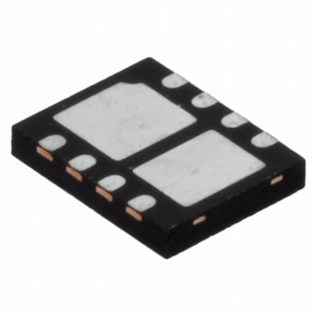
| 供应商器件封装 | 8-WSON (4x4) |
| 其它名称 | *LM25007SD/NOPB |
| 包装 | 剪切带 (CT) |
| 同步整流器 | 无 |
| 商标 | Texas Instruments |
| 安装类型 | 表面贴装 |
| 安装风格 | SMD/SMT |
| 宽度 | 4 mm |
| 封装 | Reel |
| 封装/外壳 | 8-WDFN 裸露焊盘 |
| 封装/箱体 | WSON-8 |
| 工作温度 | -40°C ~ 125°C |
| 工厂包装数量 | 1000 |
| 开关频率 | 800 kHz |
| 最大工作温度 | + 125 C |
| 最大输入电压 | 42 V |
| 最小工作温度 | - 40 C |
| 最小输入电压 | 9 V |
| 标准包装 | 1 |
| 电压-输入 | 9 V ~ 42 V |
| 电压-输出 | 2.5 V ~ 37 V |
| 电流-输出 | 500mA |
| 类型 | Step Down |
| 系列 | LM25007 |
| 设计资源 | http://www.digikey.com/product-highlights/cn/zh/texas-instruments-webench-design-center/3176 |
| 输出数 | 1 |
| 输出电压 | 2.5 V to 30 V |
| 输出电流 | 500 mA |
| 输出端数量 | 1 Output |
| 输出类型 | 可调式 |
| 配用 | /product-detail/zh/LM25007EVAL/LM25007EVAL-ND/1640590 |
| 频率-开关 | 最高 800kHz |


- 商务部:美国ITC正式对集成电路等产品启动337调查
- 曝三星4nm工艺存在良率问题 高通将骁龙8 Gen1或转产台积电
- 太阳诱电将投资9.5亿元在常州建新厂生产MLCC 预计2023年完工
- 英特尔发布欧洲新工厂建设计划 深化IDM 2.0 战略
- 台积电先进制程称霸业界 有大客户加持明年业绩稳了
- 达到5530亿美元!SIA预计今年全球半导体销售额将创下新高
- 英特尔拟将自动驾驶子公司Mobileye上市 估值或超500亿美元
- 三星加码芯片和SET,合并消费电子和移动部门,撤换高东真等 CEO
- 三星电子宣布重大人事变动 还合并消费电子和移动部门
- 海关总署:前11个月进口集成电路产品价值2.52万亿元 增长14.8%


PDF Datasheet 数据手册内容提取
LM25007 www.ti.com SNVS401C–JANUARY2006–REVISEDFEBRUARY2013 LM25007 42V, 0.5A Step-Down Switching Regulator CheckforSamples:LM25007 FEATURES DESCRIPTION 1 • Integrated0.74ΩN-ChannelMOSFETSwitch The LM25007 is a monolithic step-down switching 2 regulator featuring all of the functions needed to • Guaranteed0.5AOutputCurrent implement a low cost, efficient, power supply. • Ultra-FastTransientResponse Capable of driving a 0.5A load over a 9V-42V input • Upto800kHzOperation voltage range, this device is easy to apply and is provided in the small VSSOP-8 and the thermally • NoControlLoopCompensationRequired enhanced WSON-8 packages. Ultra-fast transient • VinFeedForwardProvidesConstant response is achieved through the use of a constant OperatingFrequency on-time architecture with Vin feed forward. This • 2%Accurate2.5VFeedbackfrom-40°Cto feature provides an almost constant operating frequency over load and input voltage variations. The 125°C operating frequency can be adjusted with a single • HighlyEfficientOperation resistor. This architecture is easy to use and tolerant • IntelligentCurrentLimitProtection of component selection. An intelligent current limit is • ExternalShutdownControl implemented in the LM25007 with forced off time that is inversely proportional to Vout thus ensuring • ThermalShutdown recovery from fault conditions. The output voltage • VSSOPandThermallyEnhancedWSON may be set from 2.5V to >30V. To improve efficiency Packages in light load applications, the Vcc pin can be connected to an external voltage source to eliminate TYPICAL APPLICATIONS the drop through the internal regulator. Additional features include: thermal shutdown, Vcc under- • 12VDCand24VDCDistributedRailSystems voltage lockout, gate drive under-voltage lockout, and • 24VACSystems maxdutycyclelimiter. • AutomotiveBodyElectronicsandTelematics • IndustrialSystems • HB-LEDConstantCurrentSource • Package: – VSSOP-8 – WSON-8(4mmx4mm) 1 Pleasebeawarethatanimportantnoticeconcerningavailability,standardwarranty,anduseincriticalapplicationsof TexasInstrumentssemiconductorproductsanddisclaimerstheretoappearsattheendofthisdatasheet. Alltrademarksarethepropertyoftheirrespectiveowners. 2 PRODUCTIONDATAinformationiscurrentasofpublicationdate. Copyright©2006–2013,TexasInstrumentsIncorporated Products conform to specifications per the terms of the Texas Instruments standard warranty. Production processing does not necessarilyincludetestingofallparameters.
LM25007 SNVS401C–JANUARY2006–REVISEDFEBRUARY2013 www.ti.com Basic Step-Down Regulator 9V – 42V Input VIN VCC 8 7 LM25007 C3 C5 C1 BST 2 GND C4 RON L1 RON/SD SW VOUT 6 1 SHUTDOWN RCL D1 R3 R5 3 RCL FB C2 RTN 5 R4 4 GND Connection Diagram 1 8 SW VIN 2 7 BST VCC 3 6 RCL RON 4 5 RTN FB 8-LeadVSSOP,WSON 2 SubmitDocumentationFeedback Copyright©2006–2013,TexasInstrumentsIncorporated ProductFolderLinks:LM25007
LM25007 www.ti.com SNVS401C–JANUARY2006–REVISEDFEBRUARY2013 PinDescriptions Pin Name Description ApplicationInformation 1 SW SwitchingNode Powerswitchingnode.Connecttotheinductor,bootstrapcapacitor,andfree-wheeling diode. 2 BST BoostBoot–strap AnexternalcapacitorisrequiredbetweentheBSTandtheSWpins.A0.01µFceramic capacitorinput capacitorisrecommended. 3 RCL CurrentLimitOFFtime AresistorbetweenthispinandRTNsetstheoff-timewhencurrentlimitisdetected. programmingpin Theoff-timeispresetto17µsifFB=0V. 4 RTN CircuitGround 5 FB FeedbackSignalfrom Thispinisconnectedtotheinvertinginputoftheinternalregulationcomparator.The RegulatedOutput regulationthresholdis2.5V. 6 RON/SD On-timesetpin AresistorbetweenthispinandVINsetstheswitchon-timeasafunctionofVin.The minimumrecommendedon-timeis300nsatthemaximuminputvoltage. 7 VCC Outputfromtheinternal Ifanauxiliaryvoltageisavailabletoraisethevoltageonthispinabovetheregulation highvoltagebias setpoint(7V),theinternalseriespassregulatorwillshutdown,reducingtheICpower regulator. dissipation.Donotexceed14V.Thisoutputprovidesgatedrivepowerfortheinternal Buckswitch.AninternaldiodeisprovidedbetweenthispinandtheBSTpin.Alocal 0.1uFdecouplingcapacitorisrecommended. 8 VIN Inputsupplyvoltage Recommendedoperatingrange:9Vto42V. - EP Exposedpad,underside ExposedmetalpadontheWSONpackageunderside.Itisrecommendedtoconnect oftheWSONpackage thispadtothePCboardgroundplanetoaidinheatdissipation. option Typical Application Circuit and Block Diagram 7V SERIES LM25007 12V -42V REGULATOR 8 VCC 7 C5 VIN SD C1 0.1 PF, C3 1 PF 100V UVLO THERMAL 0.1 PF SHUTDOWN RON ON TIMER 200k START COMPLETE 6 Ron BST 2 SD/ RON START SHUTDOWN OCVOEMRP-VAORLATTAOGRE MINIMUM OFF UVLO SD VIN TIMER C4 + DRIVER 0.01 PF 2.875V - COMPLETE 100 PH LEVEL L1 2.5V SHIFT SW 1 10V SET 5 + S Q - FB REGULATION RCLRQ COMPARATOR R3 FB COMPLETE 3.01k R5 3 RCL RCL START + SBWUITCCKH 1 - CURRENT 1R002k CUORFRFE TNITM ELIRMIT 0.725A SENSE D1 4 RTN C2 R4 15 PF 1k Copyright©2006–2013,TexasInstrumentsIncorporated SubmitDocumentationFeedback 3 ProductFolderLinks:LM25007
LM25007 SNVS401C–JANUARY2006–REVISEDFEBRUARY2013 www.ti.com Thesedeviceshavelimitedbuilt-inESDprotection.Theleadsshouldbeshortedtogetherorthedeviceplacedinconductivefoam duringstorageorhandlingtopreventelectrostaticdamagetotheMOSgates. Absolute Maximum Ratings(1) VINtoRTN 45V BSTtoRTN 59V SWtoRTN(SteadyState) -1V ESDRating,HumanBodyModel(2) 2kV BSTtoV 45V CC BSTtoSW 14V VCCtoRTN 14V AllOtherInputstoRTN -0.3to7V StorageTemperatureRange -65°Cto+150°C (1) AbsoluteMaximumRatingsarelimitsbeyondwhichdamagetothedevicemayoccur.OperatingRatingsareconditionsunderwhich operationofthedeviceisintendedtobefunctional.Forguaranteedspecificationsandtestconditions,seetheElectricalCharacteristics. (2) Thehumanbodymodelisa100pFcapacitordischargethrougha1.5kΩresistorintoeachpin.ThehumanbodyESDcompliancelevel forPin7and8is1000V. Operating Ratings(1) V 9Vto42V IN JunctionTemperature −40°Cto+125°C (1) AbsoluteMaximumRatingsarelimitsbeyondwhichdamagetothedevicemayoccur.OperatingRatingsareconditionsunderwhich operationofthedeviceisintendedtobefunctional.Forguaranteedspecificationsandtestconditions,seetheElectricalCharacteristics. 4 SubmitDocumentationFeedback Copyright©2006–2013,TexasInstrumentsIncorporated ProductFolderLinks:LM25007
LM25007 www.ti.com SNVS401C–JANUARY2006–REVISEDFEBRUARY2013 Electrical Characteristics(1) SpecificationswithstandardtypeareforT =25°Conly;limitsinboldfacetypeapplyoverthefullOperatingJunction J Temperature(T)range.MinimumandMaximumlimitsareguaranteedthroughtest,design,orstatisticalcorrelation.Typical J valuesrepresentthemostlikelyparametricnormatT =25°C,andareprovidedforreferencepurposesonly.Unless J otherwisestatedthefollowingconditionsapply:V =24V,R =200kΩ.. IN ON Symbol Parameter Conditions Min Typ Max Unit StartupRegulator V Reg V RegulatorOutput 6.6 7 7.4 V CC CC V CurrentLimit (2) 11 mA CC V Supply CC V undervoltageLockoutVoltage 6.3 V CC (V increasing) CC V UndervoltageHysteresis 206 mV CC V UVLODelay(filter) 3 µs CC OperatingCurrent(I ) Non-Switching,FB=3V 500 675 µA CC Shutdown/StandbyCurrent RON/SD=0V 70 150 µA SwitchCharacteristics BuckSwitchRds(on) I =200mA, 0.74 1.34 Ω TEST VBST−VSW=6.3V(3) GateDriveUVLO(VBST–VSW) Rising 3.4 4.5 5.5 V GateDriveUVLOHysteresis 400 mV CurrentLimit CurrentLimitThreshold 535 725 900 mA CurrentLimitResponseTime I Overdrive=0.1ATimeto 225 ns switch SwitchOff OFFtimegenerator(test1) FB=0V,RCL=100K 17 µs OFFtimegenerator(test2) FB=2.3V,RCL=100K 2.65 µs OnTimeGenerator TON-1 Vin=10V 2.15 2.77 3.5 µs Ron=200K TON-2 Vin=40V 450 615 810 ns Ron=200K RemoteShutdownThreshold Rising 0.45 0.7 1.1 V RemoteShutdownHysteresis 40 mV MinimumOffTime MinimumOffTimer FB=0V 300 ns RegulationandOVComparators FBReferenceThreshold Internalreference 2.445 2.5 2.550 V TrippointforswitchON FBOver-VoltageThreshold TrippointforswitchOFF 2.875 V FBBiasCurrent 100 nA ThermalShutdown Tsd ThermalShutdownTemp. 165 °C ThermalShutdownHysteresis 25 °C ThermalResistance θ JunctiontoAmbient DGKPackage 200 °C/W JA NGTPackage 40 °C/W (1) Alllimitsareguaranteed.AllelectricalcharacteristicshavingroomtemperaturelimitsaretestedduringproductionwithT =T =25°C. A J Allhotandcoldlimitsareguaranteedbycorrelatingtheelectricalcharacteristicstoprocessandtemperaturevariationsandapplying statisticalprocesscontrol. (2) TheV outputisintendedasaselfbiasfortheinternalgatedrivepowerandcontrolcircuits.Devicethermallimitationslimitexternal CC loading. (3) FordevicesprocuredintheWSON-8packagetheRds(on)limitsareguaranteedbydesigncharacterizationdataonly. Copyright©2006–2013,TexasInstrumentsIncorporated SubmitDocumentationFeedback 5 ProductFolderLinks:LM25007
LM25007 SNVS401C–JANUARY2006–REVISEDFEBRUARY2013 www.ti.com Typical Performance Characteristics OperationalWaveforms OperationalWaveforms LM25007Operation:V =10V,V =20V,I =250mA OUT IN OUT LM25007Operation:V =10V,V =42V,I =250mA CH1:SwitchNode,CH2:V (AC),CH4:InductorCurrent OUT IN OUT OUT CH1:SwitchNode,CH2:V (AC),CH4:InductorCurrent OUT Figure1. Figure2. CurrentLimitOff-Time LM2500710VOutputEfficiency vsV FB 100 20 18 VIN = 15V 16 600k )% 90 14 400k 200k ( YC 30V )sP 12 NE ( F 10 ICIF 42V TFO 8 F 80 E 6 4 2 100k 50k 70 0 0 100 200 300 400 500 0 0.5 1 1.5 2 2.5 LOAD CURRENT (mA) V (V) FB Figure3. Figure4. V IN vsT ON R =100k,200k,300k ON 10000 RON = 300k )s n ( E M 1000 IT-N 200k O 100k 100 0 10 20 30 42 INPUT VOLTAGE VIN (V) Figure5. 6 SubmitDocumentationFeedback Copyright©2006–2013,TexasInstrumentsIncorporated ProductFolderLinks:LM25007
LM25007 www.ti.com SNVS401C–JANUARY2006–REVISEDFEBRUARY2013 DETAILED OPERATING DESCRIPTION The LM25007 is a monolithic step-down switching regulator featuring all of the functions needed to implement low cost, efficient, power supply. Capable of driving a 0.5Amp load over a 9-42V input voltage range, this device iseasytoapplyandisprovidedinthesmallVSSOP-8andthethermallyenhancedWSON-8packages.Ultra-fast transient response is achieved through the use of a constant on-time architecture with Vin feed forward. This feature provides and almost constant operating frequency over load and input voltage variations. The operating frequency may be adjusted up to 800kHz depending on input and output voltages. This architecture is easy to use and tolerant of component selection. An intelligent current limit is implemented in the LM25007 with forced off time that is inversely proportional to Vout to ensure recovery from fault conditions. The output voltage may be set from 2.5V to >30V. To improve efficiency in light load applications, the Vcc pin can be tied to an external voltage source thus eliminating the drop through the integrated internal regulator. Additional protection features include: thermal shutdown, Vcc under-voltage lockout, gate drive under-voltage lockout, and max duty cycle limiter. Hysteretic Control Circuit Overview The LM25007 is a Buck DC-DC regulator that uses a constant on-time control scheme. The on-time is programmed by an external resistor and varies inversely with line input voltage (Vin). The core regulation elements of the LM25007 are the feedback comparator and the on-time one-shot. The regulator output voltage is sensed at the feedback pin (FB) and is compared to an internal reference voltage (2.5V). If the FB signal is below the reference voltage, the buck switch is turned on for a fixed time pulse determined by the line voltage and a programming resistor (R ). Following the on period the switch will remain off for at least the minimum off ON timerperiodof300ns.IftheFBpinvoltageisstillbelowthereferenceafterthe300nsoff-time,theswitchwillturn on again for another on time period. This switching behavior will continue until the FB pin voltage reaches the referencevoltagelevel. The LM25007 operates in discontinuous conduction mode at light load currents or continuous conduction mode atheavierloadcurrents.Indiscontinuousconductionmode,currentthroughtheoutputinductorstartsatzeroand ramps up to a peak value during the buck switch on-time and then back to zero during the off-time. The inductor current remains at zero until the next on-time period starts when FB falls below the internal reference. In discontinuous mode the operating frequency is relatively low and will vary with load. Therefore at light loads the conversion efficiency is maintained, since the switching losses decrease with the reduction in load current and switchingfrequency.Theapproximatediscontinuousmodeoperatingfrequencycanbecalculatedasfollows: V 2 x L OUT F = 1 x 10-20 x R x (R )2 Load ON (1) In continuous conduction mode, current flows continuously through the inductor and never ramps down to zero. In this mode the operating frequency is greater than the discontinuous mode frequency and remains relatively constant with load and line variations. The approximate continuous mode operating frequency can be calculated asfollows: V OUT F = 1.42 x 10⁻¹⁰ x R ON (2) The output voltage (Vout) can be programmed by two external resistors as shown in Figure 6. The regulated voltageiscalculatedasfollows: V =2.5x(R3+R4)/R4 (3) OUT The feedback comparator in hysteretic regulators depends on the output ripple voltage to switch the output transistor on and off at regular intervals. In order for the internal comparator to respond quickly to changes in output voltage, proportional to inductor current, a minimum amount of capacitor Equivalent Series Resistance (ESR) is required. A ripple voltage of 25mV is recommended at the feedback pin (FB) for stable operation. In caseswheretheintrinsiccapacitorESRistoosmall,additionalseriesresistancemaybeadded. Copyright©2006–2013,TexasInstrumentsIncorporated SubmitDocumentationFeedback 7 ProductFolderLinks:LM25007
LM25007 SNVS401C–JANUARY2006–REVISEDFEBRUARY2013 www.ti.com For applications where lower output voltage ripple is required the load can be connected directly to the low ESR output capacitor, as shown in Figure 6. The series resistor (R5) will degrade the load regulation. Another technique for enhancing the ripple voltage at the FB pin is to place a capacitor in parallel with the feedback divider resistor R3. The addition of the capacitor reduces the attenuation of the ripple voltage from the feedback divider. High Voltage Bias Regulator (VCC) The LM25007 contains an internal high voltage bias regulator. The input pin (Vin) can be connected directly to line voltages from 9 to 42 Volts. To avoid supply voltage transients due to long lead inductances on the input pin (VIN), it is always recommended to connect a low ESR ceramic chip capacitor (≊ 0.1µF) between VIN and RTN pins located close to the LM25007. The regulator is internally current limited to 11mA. Upon power up, the regulator is enabled and sources current into an external capacitor connected to the VCC pin. When the voltage ontheVCCpinreachesitsUVLOlevel(6.3V),thecontrolleroutputisenabled. AnexternalauxiliarysupplyvoltagecanbediodeconnectedtotheVccpin.Iftheauxiliaryvoltageisgreaterthan 7 Volts the internal regulator will shutoff, thus reducing internal power dissipation. Do not exceed 14V at VCC. SeeFigure7. VIN L SW R3 R5 FB + VOUT - + COUT R4 REF 2.5V LM25007 Figure6. LowRippleOutputConfiguration 8 SubmitDocumentationFeedback Copyright©2006–2013,TexasInstrumentsIncorporated ProductFolderLinks:LM25007
LM25007 www.ti.com SNVS401C–JANUARY2006–REVISEDFEBRUARY2013 7V SERIES REGULATOR VCC + 0.1 PF SELF-BIAS DIODE BST VIN + 0.01 PF SW LM25007 10V 30k + 10k Figure7. SelfBiasedConfiguration Over-Voltage Comparator The over-voltage comparator is provided to protect the output from overvoltage conditions due to sudden input line voltage changes or output loading changes. The over-voltage comparator monitors the FB pin versus an internal 2.875V reference. If the voltage at FB rises above 2.875V the comparator immediately terminates the buckswitchon-timepulse. ON Time generator and Shutdown The on-time of the LM25007 is set inversely proportional to the input voltage by an external resistor connected between RON/SD and VIN. The RON/SD terminal is a low impedance input biased at approximately 1.5V. The current through the resistor and into the RON/SD pin is approximately proportional to Vin and used internally to control the on-timer. This scheme of input voltage feed-forward hysteretic operation achieves nearly constant operationalfrequencyovervaryinglineandloadconditions.Theon-timeequationfortheLM25007is: Ton=1.42x10⁻¹⁰xR /V (4) ON IN The RON/SD pin of the LM25007 also provides a shutdown function which disables the regulator and significantly decreases quiescent power dissipation. By pulling the pin below 0.7V activates the low power shutdown mode. The V quiescent current in the shutdown mode is approximately 100µA internal to the IN LM25007plusthecurrentintheR resistor.SeeFigure8. ON Copyright©2006–2013,TexasInstrumentsIncorporated SubmitDocumentationFeedback 9 ProductFolderLinks:LM25007
LM25007 SNVS401C–JANUARY2006–REVISEDFEBRUARY2013 www.ti.com 7V SERIES REGULATOR VIN VIN ON TIMER RON VIN START RON/SD RON COMPLETE STOP RUN LM25007 Figure8. ShutdownImplementation Current Limit The LM25007 contains an intelligent current limit off-timer intended to reduce the foldback characteristic inherent with fixed off-time over-current protection. If the current in the Buck switch exceeds 725mA the present cycle on- time is immediately terminated (cycle by cycle current limit). Following the termination of the cycle a non- resetable current limit off timer is initiated. The duration of the off time is a function of the external resistor (RCL) and the FB pin voltage. When the FB pin voltage equals zero, the current limit off-time is internally preset to 17µs.Thisconditionoccursinshortcircuitoperationwhenamaximumamountofoff-timeisrequired. In cases of overload (not complete short circuit) the current limit off-time is reduced as a function of the output voltage (measured at the FB pin). Reducing the off-time with smaller overloads reduces the amount of foldback andalsoreducestheinitialstart-uptime.ThecurrentlimitofftimeforagivenFBpinvoltageandR resistorcan CL becalculatedbythefollowingequation: Toff=10-5/(0.59+(V /7.22x10-6xR )) (5) FB CL Applications utilizing low resistance inductors and/or a low voltage drop rectifier may require special evaluation at high line, short circuit conditions. In this special case the preset 17µs (FB = 0V) off-time may be insufficient to balance the inductor volt*time product. Additional inductor resistance, output resistance or a larger voltage drop rectifiermaybenecessarytobalancetheinductorcyclevolt*timeproductandlimittheshortcircuitcurrent. N - Channel Buck Switch and Driver The LM25007 integrates an N-Channel Buck switch and associated floating high voltage gate driver. The gate driver circuit works in conjunction with an external bootstrap capacitor and an internal high voltage diode. The bootstrap capacitor is charged by V through the internal high voltage diode. A 0.01uF ceramic capacitor CC connectedbetweentheBSTpinandSWpinisrecommended. During each cycle when the Buck switch turns off, the SW pin is approximately 0V. When the SW pin voltage is low, the bootstrap capacitor is charged from Vcc through the internal diode. The minimum off timer, set to 300ns, ensuresthattherewillbeaminimumintervaleverycycletorechargethebootstrapcapacitor. An external re-circulating diode from the SW pin to ground is necessary to carry the inductor current after the internal Buck switch turns off. This external diode must be of the Ultra-fast or Schottky type to reduce turn-on losses and current over-shoot. The reverse voltage rating of the re-circulating diode must be greater than the maximumlineinputvoltage. 10 SubmitDocumentationFeedback Copyright©2006–2013,TexasInstrumentsIncorporated ProductFolderLinks:LM25007
LM25007 www.ti.com SNVS401C–JANUARY2006–REVISEDFEBRUARY2013 Thermal Protection InternalThermalShutdowncircuitryisprovidedtoprotecttheintegratedcircuitintheeventthemaximumjunction temperature is exceeded. When thermal protection is activated, typically at 165 degrees Celsius, the controller is forced into a low power reset state, disabling the output driver. This feature is provided to prevent catastrophic failuresfromaccidentaldeviceoverheating. Minimum Load Current Aminimumloadcurrentof1mAisrequiredtomaintainproperoperation.Iftheloadcurrentfallsbelowthatlevel, the bootstrap capacitor may discharge during the long off-time, and the circuitwill either shutdown, or cycle on and off at a low frequency. If the load current is expected to drop below 1 mA in the application, the feedback resistorsshouldbechosenlowenoughinvaluesotheyprovidetheminimumrequiredcurrentatnominalVout. 10V, 400mA Demo Board Bill of Materials SeeTypicalApplicationCircuitandBlockDiagram Table1.BillofMaterials ITEM PARTNUMBER DESCRIPTION VALUE C1 C4532X7R2A105M CAPACITOR,CER,TDK 1µ,100V C2 C4532X7R1E156M CAPACITOR,CER,TDK 15µ,25V C3 C1206C104K5RAC CAPACITOR,CER,KEMET 0.1µ,50V C4 C1206C103K5RAC CAPACITOR,CER,KEMET 0.01µ,50V C5 C3216X7R2A104KT CAPACITOR,CER,TDK 0.1µ,100V D1 MURA110T3 DIODE,100V,ONSEMI L1 SLF7045T-101MR60-1 BUCKINDUCTOR,TDK 100µH R1 CRCW12062003F RESISTOR 200K R2 CRCW12061003F RESISTOR 100K R3 CRCW12063011F RESISTOR 3.01K R4 CRCW12061001F RESISTOR 1K R5 CRCW12061R00F RESISTOR 1 U1 LM25007 REGULATOR,TI Copyright©2006–2013,TexasInstrumentsIncorporated SubmitDocumentationFeedback 11 ProductFolderLinks:LM25007
LM25007 SNVS401C–JANUARY2006–REVISEDFEBRUARY2013 www.ti.com REVISION HISTORY ChangesfromRevisionB(February2013)toRevisionC Page • ChangedlayoutofNationalDataSheettoTIformat.......................................................................................................... 11 12 SubmitDocumentationFeedback Copyright©2006–2013,TexasInstrumentsIncorporated ProductFolderLinks:LM25007
PACKAGE OPTION ADDENDUM www.ti.com 6-Feb-2020 PACKAGING INFORMATION Orderable Device Status Package Type Package Pins Package Eco Plan Lead/Ball Finish MSL Peak Temp Op Temp (°C) Device Marking Samples (1) Drawing Qty (2) (6) (3) (4/5) LM25007MM NRND VSSOP DGK 8 1000 TBD Call TI Call TI -40 to 125 SLYB LM25007MM/NOPB ACTIVE VSSOP DGK 8 1000 Green (RoHS SN Level-1-260C-UNLIM -40 to 125 SLYB & no Sb/Br) LM25007MMX/NOPB ACTIVE VSSOP DGK 8 3500 Green (RoHS SN Level-1-260C-UNLIM -40 to 125 SLYB & no Sb/Br) LM25007SD/NOPB ACTIVE WSON NGT 8 1000 Green (RoHS SN Level-1-260C-UNLIM -40 to 125 25007SD & no Sb/Br) LM25007SDX/NOPB ACTIVE WSON NGT 8 4500 Green (RoHS SN Level-1-260C-UNLIM -40 to 125 25007SD & no Sb/Br) (1) The marketing status values are defined as follows: ACTIVE: Product device recommended for new designs. LIFEBUY: TI has announced that the device will be discontinued, and a lifetime-buy period is in effect. NRND: Not recommended for new designs. Device is in production to support existing customers, but TI does not recommend using this part in a new design. PREVIEW: Device has been announced but is not in production. Samples may or may not be available. OBSOLETE: TI has discontinued the production of the device. (2) RoHS: TI defines "RoHS" to mean semiconductor products that are compliant with the current EU RoHS requirements for all 10 RoHS substances, including the requirement that RoHS substance do not exceed 0.1% by weight in homogeneous materials. Where designed to be soldered at high temperatures, "RoHS" products are suitable for use in specified lead-free processes. TI may reference these types of products as "Pb-Free". RoHS Exempt: TI defines "RoHS Exempt" to mean products that contain lead but are compliant with EU RoHS pursuant to a specific EU RoHS exemption. Green: TI defines "Green" to mean the content of Chlorine (Cl) and Bromine (Br) based flame retardants meet JS709B low halogen requirements of <=1000ppm threshold. Antimony trioxide based flame retardants must also meet the <=1000ppm threshold requirement. (3) MSL, Peak Temp. - The Moisture Sensitivity Level rating according to the JEDEC industry standard classifications, and peak solder temperature. (4) There may be additional marking, which relates to the logo, the lot trace code information, or the environmental category on the device. (5) Multiple Device Markings will be inside parentheses. Only one Device Marking contained in parentheses and separated by a "~" will appear on a device. If a line is indented then it is a continuation of the previous line and the two combined represent the entire Device Marking for that device. (6) Lead/Ball Finish - Orderable Devices may have multiple material finish options. Finish options are separated by a vertical ruled line. Lead/Ball Finish values may wrap to two lines if the finish value exceeds the maximum column width. Addendum-Page 1
PACKAGE OPTION ADDENDUM www.ti.com 6-Feb-2020 Important Information and Disclaimer:The information provided on this page represents TI's knowledge and belief as of the date that it is provided. TI bases its knowledge and belief on information provided by third parties, and makes no representation or warranty as to the accuracy of such information. Efforts are underway to better integrate information from third parties. TI has taken and continues to take reasonable steps to provide representative and accurate information but may not have conducted destructive testing or chemical analysis on incoming materials and chemicals. TI and TI suppliers consider certain information to be proprietary, and thus CAS numbers and other limited information may not be available for release. In no event shall TI's liability arising out of such information exceed the total purchase price of the TI part(s) at issue in this document sold by TI to Customer on an annual basis. Addendum-Page 2
PACKAGE MATERIALS INFORMATION www.ti.com 29-Sep-2019 TAPE AND REEL INFORMATION *Alldimensionsarenominal Device Package Package Pins SPQ Reel Reel A0 B0 K0 P1 W Pin1 Type Drawing Diameter Width (mm) (mm) (mm) (mm) (mm) Quadrant (mm) W1(mm) LM25007MM VSSOP DGK 8 1000 178.0 12.4 5.3 3.4 1.4 8.0 12.0 Q1 LM25007MM/NOPB VSSOP DGK 8 1000 178.0 12.4 5.3 3.4 1.4 8.0 12.0 Q1 LM25007MMX/NOPB VSSOP DGK 8 3500 330.0 12.4 5.3 3.4 1.4 8.0 12.0 Q1 LM25007SD/NOPB WSON NGT 8 1000 178.0 12.4 4.3 4.3 1.3 8.0 12.0 Q1 LM25007SDX/NOPB WSON NGT 8 4500 330.0 12.4 4.3 4.3 1.3 8.0 12.0 Q1 PackMaterials-Page1
PACKAGE MATERIALS INFORMATION www.ti.com 29-Sep-2019 *Alldimensionsarenominal Device PackageType PackageDrawing Pins SPQ Length(mm) Width(mm) Height(mm) LM25007MM VSSOP DGK 8 1000 210.0 185.0 35.0 LM25007MM/NOPB VSSOP DGK 8 1000 210.0 185.0 35.0 LM25007MMX/NOPB VSSOP DGK 8 3500 367.0 367.0 35.0 LM25007SD/NOPB WSON NGT 8 1000 210.0 185.0 35.0 LM25007SDX/NOPB WSON NGT 8 4500 367.0 367.0 35.0 PackMaterials-Page2
MECHANICAL DATA NGT0008A SDC08A (Rev A) www.ti.com
None
None
IMPORTANTNOTICEANDDISCLAIMER TI PROVIDES TECHNICAL AND RELIABILITY DATA (INCLUDING DATASHEETS), DESIGN RESOURCES (INCLUDING REFERENCE DESIGNS), APPLICATION OR OTHER DESIGN ADVICE, WEB TOOLS, SAFETY INFORMATION, AND OTHER RESOURCES “AS IS” AND WITH ALL FAULTS, AND DISCLAIMS ALL WARRANTIES, EXPRESS AND IMPLIED, INCLUDING WITHOUT LIMITATION ANY IMPLIED WARRANTIES OF MERCHANTABILITY, FITNESS FOR A PARTICULAR PURPOSE OR NON-INFRINGEMENT OF THIRD PARTY INTELLECTUAL PROPERTY RIGHTS. These resources are intended for skilled developers designing with TI products. You are solely responsible for (1) selecting the appropriate TI products for your application, (2) designing, validating and testing your application, and (3) ensuring your application meets applicable standards, and any other safety, security, or other requirements. These resources are subject to change without notice. TI grants you permission to use these resources only for development of an application that uses the TI products described in the resource. Other reproduction and display of these resources is prohibited. No license is granted to any other TI intellectual property right or to any third party intellectual property right. TI disclaims responsibility for, and you will fully indemnify TI and its representatives against, any claims, damages, costs, losses, and liabilities arising out of your use of these resources. TI’s products are provided subject to TI’s Terms of Sale (www.ti.com/legal/termsofsale.html) or other applicable terms available either on ti.com or provided in conjunction with such TI products. TI’s provision of these resources does not expand or otherwise alter TI’s applicable warranties or warranty disclaimers for TI products. Mailing Address: Texas Instruments, Post Office Box 655303, Dallas, Texas 75265 Copyright © 2020, Texas Instruments Incorporated