ICGOO在线商城 > 集成电路(IC) > PMIC - 稳压器 - DC DC 开关稳压器 > MC34063ADRJR
 Datasheet下载
- 型号: MC34063ADRJR
- 制造商: Texas Instruments
- 库位|库存: xxxx|xxxx
- 要求:
| 数量阶梯 | 香港交货 | 国内含税 |
| +xxxx | $xxxx | ¥xxxx |
查看当月历史价格
查看今年历史价格
MC34063ADRJR产品简介:
ICGOO电子元器件商城为您提供MC34063ADRJR由Texas Instruments设计生产,在icgoo商城现货销售,并且可以通过原厂、代理商等渠道进行代购。 MC34063ADRJR价格参考¥询价-¥询价。Texas InstrumentsMC34063ADRJR封装/规格:PMIC - 稳压器 - DC DC 开关稳压器, Buck, Boost Switching Regulator IC Positive or Negative Adjustable 1.25V 1 Output 1.5A (Switch) 8-WDFN Exposed Pad。您可以下载MC34063ADRJR参考资料、Datasheet数据手册功能说明书,资料中有MC34063ADRJR 详细功能的应用电路图电压和使用方法及教程。
MC34063ADRJR是德州仪器(Texas Instruments)推出的一款DC-DC开关稳压器,属于PMIC类电源管理芯片。该器件集成了一个温度补偿基准电压源、比较器、占空比可控的振荡器、驱动晶体管和高电流输出开关,适用于升压(Boost)、降压(Buck)及反相(Inverting)等多种DC-DC转换拓扑结构。

其典型应用场景包括:消费类电子产品中的电池供电系统,如便携式音频设备、小型显示器和LED驱动电源;工业控制领域的小功率电源模块,用于将不稳定的输入电压(如5V或12V)转换为稳定输出(如3.3V或15V);通信设备中作为板级电源转换电路,支持低功耗传感器、微控制器和接口电路的供电需求;此外,也广泛应用于汽车电子中的辅助电源系统,例如车载仪表或小型充电模块。

MC34063ADRJR采用SOIC-8封装,具有体积小、外围元件少、成本低的优点,适合对空间和成本敏感的设计。其工作温度范围宽(-40°C 至 +85°C),具备较好的环境适应性。虽然效率相较于现代同步整流芯片略低,但因其成熟可靠、易于设计,在中小功率、非高效率要求的应用中仍被广泛使用。
| 参数 | 数值 |
| 产品目录 | 集成电路 (IC)半导体 |
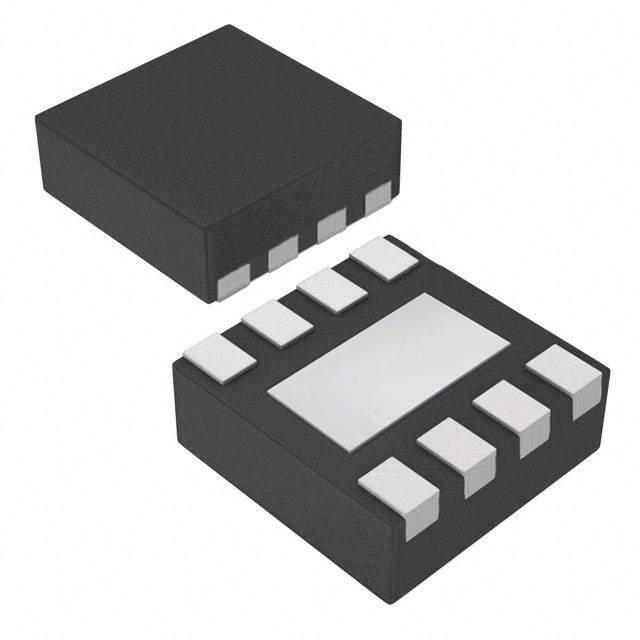
| 描述 | IC REG BUCK BOOST INV ADJ 8-SON稳压器—开关式稳压器 1.5A Boost/Buck/ Inverting Sw Reg |
| 产品分类 | |
| 品牌 | Texas Instruments |
| 产品手册 | |
| 产品图片 |
|
| rohs | 符合RoHS无铅 / 符合限制有害物质指令(RoHS)规范要求 |
| 产品系列 | 电源管理 IC,稳压器—开关式稳压器,Texas Instruments MC34063ADRJR- |
| 数据手册 | |
| 产品型号 | MC34063ADRJR |
| PWM类型 | - |
| 产品目录页面 | |
| 产品种类 | 稳压器—开关式稳压器 |
| 供应商器件封装 | 8-SON 裸露焊盘(4x4) |
| 其它名称 | 296-21745-2 |
| 包装 | 带卷 (TR) |
| 同步整流器 | 无 |
| 商标 | Texas Instruments |
| 安装类型 | 表面贴装 |
| 安装风格 | SMD/SMT |
| 封装 | Reel |
| 封装/外壳 | 8-WDFN 裸露焊盘 |
| 封装/箱体 | WSON-8 |
| 工作温度 | 0°C ~ 70°C |
| 工厂包装数量 | 1000 |
| 开关频率 | 100 kHz |
| 拓扑结构 | Buck, Boost, Inverting |
| 最大工作温度 | + 70 C |
| 最大输入电压 | 40 V |
| 最小工作温度 | 0 C |
| 标准包装 | 1,000 |
| 电压-输入 | 3 V ~ 40 V |
| 电压-输出 | 1.55 V ~ 40 V |
| 电流-输出 | 1.5A |
| 类型 | 降压(降压),升压(升压),反相 |
| 系列 | MC34063A |
| 输出数 | 1 |
| 输出电压 | 1.55 V to 40 V |
| 输出电流 | 1.5 A |
| 输出端数量 | 1 Output |
| 输出类型 | 可调式 |
| 频率-开关 | 100kHz |


PDF Datasheet 数据手册内容提取
Product Sample & Technical Tools & Support & Folder Buy Documents Software Community MC33063A,MC34063A SLLS636N–DECEMBER2004–REVISEDJANUARY2015 MC3x063A 1.5-A Peak Boost/Buck/Inverting Switching Regulators 1 Features 3 Description • WideInputVoltageRange:3Vto40V The MC33063A and MC34063A devices are easy-to- 1 use ICs containing all the primary circuitry needed for • HighOutputSwitchCurrent:Upto1.5A building simple DC-DC converters. These devices • AdjustableOutputVoltage primarily consist of an internal temperature- • OscillatorFrequencyUpto100kHz compensated reference, a comparator, an oscillator, a PWM controller with active current limiting, a driver, • PrecisionInternalReference:2% and a high-current output switch. Thus, the devices • Short-CircuitCurrentLimiting require minimal external components to build • LowStandbyCurrent converters in the boost, buck, and inverting topologies. 2 Applications The MC33063A device is characterized for operation • BloodGasAnalyzers:Portable from –40°C to 85°C, while the MC34063A device is characterizedforoperationfrom0°Cto70°C. • CableSolutions • HMIs(HumanMachineInterfaces) DeviceInformation(1) • Telecommunications PARTNUMBER PACKAGE(PIN) BODYSIZE • PortableDevices SOIC(8) 4.90mm×3.91mm • Consumer&Computing MC3x063A SON(8) 4.00mm×4.00mm • Test& Measurement PDIP(8) 9.81mm×6.35mm (1) For all available packages, see the orderable addendum at theendofthedatasheet. 4 Simplified Schematic Drive 8 1 Switch Collector Collector S Q Q2 Q1 R 100W Ipk 7 2 Switch Sense Emitter Ipk Oscillator CT 6 3 Timing VCC Capacitor 1.25-V + Reference Regulator − Comparator 5 4 GND Inverting Input 1 An IMPORTANT NOTICE at the end of this data sheet addresses availability, warranty, changes, use in safety-critical applications, intellectualpropertymattersandotherimportantdisclaimers.PRODUCTIONDATA.
MC33063A,MC34063A SLLS636N–DECEMBER2004–REVISEDJANUARY2015 www.ti.com Table of Contents 1 Features.................................................................. 1 8.1 Overview...................................................................7 2 Applications........................................................... 1 8.2 FunctionalBlockDiagram.........................................7 3 Description............................................................. 1 8.3 FeatureDescription...................................................7 8.4 DeviceFunctionalModes..........................................7 4 SimplifiedSchematic............................................. 1 9 ApplicationandImplementation.......................... 8 5 RevisionHistory..................................................... 2 9.1 ApplicationInformation..............................................8 6 PinConfigurationandFunctions......................... 3 9.2 TypicalApplication....................................................9 7 Specifications......................................................... 4 10 PowerSupplyRecommendations..................... 17 7.1 AbsoluteMaximumRatings......................................4 11 Layout................................................................... 17 7.2 ESDRatings..............................................................4 11.1 LayoutGuidelines.................................................17 7.3 RecommendedOperatingConditions.......................4 11.2 LayoutExample....................................................17 7.4 ThermalInformation..................................................4 12 DeviceandDocumentationSupport................. 18 7.5 ElectricalCharacteristics—Oscillator........................4 7.6 ElectricalCharacteristics—OutputSwitch.................5 12.1 RelatedLinks........................................................18 7.7 ElectricalCharacteristics—Comparator....................5 12.2 Trademarks...........................................................18 7.8 ElectricalCharacteristics—TotalDevice...................5 12.3 ElectrostaticDischargeCaution............................18 7.9 TypicalCharacteristics..............................................6 12.4 Glossary................................................................18 8 DetailedDescription.............................................. 7 13 Mechanical,Packaging,andOrderable Information........................................................... 18 5 Revision History ChangesfromRevisionM(January2011)toRevisionN Page • AddedApplications,DeviceInformationtable,PinFunctionstable,ESDRatingstable,ThermalInformationtable, FeatureDescriptionsection,DeviceFunctionalModes,ApplicationandImplementationsection,PowerSupply Recommendationssection,Layoutsection,DeviceandDocumentationSupportsection,andMechanical, Packaging,andOrderableInformationsection...................................................................................................................... 1 • DeletedOrderingInformationtable........................................................................................................................................ 1 2 SubmitDocumentationFeedback Copyright©2004–2015,TexasInstrumentsIncorporated ProductFolderLinks:MC33063A MC34063A
MC33063A,MC34063A www.ti.com SLLS636N–DECEMBER2004–REVISEDJANUARY2015 6 Pin Configuration and Functions D(SOIC) OR P(PDIP) PACKAGE (TOPVIEW) Switch Collector 1 8 Driver Collector Switch Emitter 2 7 Ipk Timing Capacitor 3 6 VCC GND 4 5 Comparator Inverting Input DRJ (QFN) PACKAGE (TOPVIEW) Switch Collector 1 † 8 Driver Collector Switch Emitter 2 7 Ipk Timing Capacitor 3 6 VCC GND 4 5 Comparator Inverting Input †The exposed thermal pad is electrically bonded internally to pin 4 (GND) . PinFunctions PIN TYPE DESCRIPTION NAME NO. SwitchCollector 1 I/O High-currentinternalswitchcollectorinput. SwitchEmitter 2 I/O High-currentinternalswitchemitteroutput. TimingCapacitor 3 — Attachatimingcapacitortochangetheswitchingfrequency. GND 4 — Ground Comparator 5 I Attachtoaresistordividernetworktocreateafeedbackloop. InvertingInput V 6 I Logicsupplyvoltage.TietoV . CC IN I 7 I Current-limitsenseinput. PK DriverCollector 8 I/O Darlingtonpairdrivingtransistorcollectorinput. Copyright©2004–2015,TexasInstrumentsIncorporated SubmitDocumentationFeedback 3 ProductFolderLinks:MC33063A MC34063A
MC33063A,MC34063A SLLS636N–DECEMBER2004–REVISEDJANUARY2015 www.ti.com 7 Specifications 7.1 Absolute Maximum Ratings overoperatingfree-airtemperaturerange(unlessotherwisenoted)(1) MIN MAX UNIT V Supplyvoltage 40 V CC V Comparatorinvertinginputvoltagerange –0.3 40 V IR V Switchcollectorvoltage 40 V C(switch) V Switchemittervoltage V =40V 40 V E(switch) PIN1 V Switchcollectortoswitchemittervoltage 40 V CE(switch) V Drivercollectorvoltage 40 V C(driver) I Drivercollectorcurrent 100 mA C(driver) I Switchcurrent 1.5 A SW T Operatingvirtualjunctiontemperature 150 °C J T Storagetemperaturerange –65 150 °C stg (1) StressesbeyondthoselistedunderAbsoluteMaximumRatingsmaycausepermanentdamagetothedevice.Thesearestressratings only,andfunctionaloperationofthedeviceattheseoranyotherconditionsbeyondthoseindicatedunderRecommendedOperating Conditionsisnotimplied.Exposuretoabsolute-maximum-ratedconditionsforextendedperiodsmayaffectdevicereliability. 7.2 ESD Ratings VALUE UNIT Humanbodymodel(HBM),perANSI/ESDA/JEDECJS-001,allpins(1) 2500 V(ESD) Electrostaticdischarge Chargeddevicemodel(CDM),perJEDECspecificationJESD22-C101, V allpins(2) 1500 (1) JEDECdocumentJEP155statesthat500-VHBMallowssafemanufacturingwithastandardESDcontrolprocess. (2) JEDECdocumentJEP157statesthat250-VCDMallowssafemanufacturingwithastandardESDcontrolprocess. 7.3 Recommended Operating Conditions MIN MAX UNIT V Supplyvoltage 3 40 V CC MC33063A –40 85 T Operatingfree-airtemperature °C A MC34063A 0 70 7.4 Thermal Information MC33063A THERMALMETRIC(1) D DRJ P UNIT 8PINS R Junction-to-ambientthermalresistance 97 41 85 °C/W θJA (1) Formoreinformationabouttraditionalandnewthermalmetrics,seetheICPackageThermalMetricsapplicationreport(SPRA953). 7.5 Electrical Characteristics—Oscillator V =5V,T =fulloperatingrange(unlessotherwisenoted)(seeblockdiagram) CC A PARAMETER TESTCONDITIONS T MIN TYP MAX UNIT A f Oscillatorfrequency V =0V,C =1nF 25°C 24 33 42 kHz osc PIN5 T I Chargecurrent V =5Vto40V 25°C 24 35 42 μA chg CC I Dischargecurrent V =5Vto40V 25°C 140 220 260 μA dischg CC I /I Discharge-to-chargecurrentratio V =V 25°C 5.2 6.5 7.5 — dischg chg PIN7 CC V Current-limitsensevoltage I =I 25°C 250 300 350 mV Ipk dischg chg 4 SubmitDocumentationFeedback Copyright©2004–2015,TexasInstrumentsIncorporated ProductFolderLinks:MC33063A MC34063A
MC33063A,MC34063A www.ti.com SLLS636N–DECEMBER2004–REVISEDJANUARY2015 7.6 Electrical Characteristics—Output Switch V =5V,T =fulloperatingrange(unlessotherwisenoted)(seeblockdiagram)(1) CC A PARAMETER TESTCONDITIONS T MIN TYP MAX UNIT A Saturationvoltage– V I =1A,pins1and8connected Fullrange 1 1.3 V CE(sat) Darlingtonconnection SW Saturationvoltage– I =1A,R =82ΩtoV , VCE(sat) non-Darlingtonconnection(2) fSoWrcedβ∼20PIN8 CC Fullrange 0.45 0.7 V h DCcurrentgain I =1A,V =5V 25°C 50 75 — FE SW CE I Collectoroff-statecurrent V =40V Fullrange 0.01 100 μA C(off) CE (1) Lowduty-cyclepulsetestingisusedtomaintainjunctiontemperatureasclosetoambienttemperatureaspossible. (2) Inthenon-Darlingtonconfiguration,iftheoutputswitchisdrivenintohardsaturationatlowswitchcurrents(≤300mA)andhighdriver currents(≥30mA),itmaytakeupto2μsfortheswitchtocomeoutofsaturation.Thisconditioneffectivelyshortenstheofftimeat frequencies≥30kHz,becomingmagnifiedastemperatureincreases.Thefollowingoutputdriveconditionisrecommendedinthenon- Darlingtonconfiguration: Forcedβofoutputswitch=I /(I –7mA)≥10,where∼7mAisrequiredbythe100-Ωresistorintheemitterofthedriverto C,SW C,driver forwardbiastheV oftheswitch. be 7.7 Electrical Characteristics—Comparator V =5V,T =fulloperatingrange(unlessotherwisenoted)(seeblockdiagram) CC A PARAMETER TESTCONDITIONS T MIN TYP MAX UNIT A 25°C 1.225 1.25 1.275 V Thresholdvoltage V th Fullrange 1.21 1.29 ΔV Threshold-voltagelineregulation V =5Vto40V Fullrange 1.4 5 mV th CC I Inputbiascurrent V =0V Fullrange –20 –400 nA IB IN 7.8 Electrical Characteristics—Total Device V =5V,T =fulloperatingrange(unlessotherwisenoted)(seeblockdiagram) CC A PARAMETER TESTCONDITIONS T MIN MAX UNIT A V =5Vto40V,C =1nF, CC T I Supplycurrent V =V ,V >V , Fullrange 4 mA CC PIN7 CC PIN5 th V =GND,Allotherpinsopen PIN2 Copyright©2004–2015,TexasInstrumentsIncorporated SubmitDocumentationFeedback 5 ProductFolderLinks:MC33063A MC34063A
MC33063A,MC34063A SLLS636N–DECEMBER2004–REVISEDJANUARY2015 www.ti.com 7.9 Typical Characteristics 1000 1.8 VCC=5V 1.7 VCC= 5 V utSwitch me(µs) 100 PPTiiAnn=752==5°VGCCNCD tON put Switcholtage (V) 11..56 PPTAiinn= 13 2,, 575°, C =8 G=N VDCC t,OutpON-OFF On-OffTi 10 tOFF V, OutCE(SAT)Saturation V 1111....1234 1 1.10 00.0 0.2 0.4 0.6 0.8 11.0 1.2 1.4 1.6 0.01 0.1 1 10 CT,OscillatorTimingCapacitor(nF) IE, Emitter Current (A) Figure2.OutputSwitchSaturationVoltagevs Figure1.OutputSwitchOn-OffTimevs EmitterCurrent(Emitter-FollowerConfiguration) OscillatorTimingCapacitor 1.4 3.6 Darlington Connection 1.2 A) 3.2 h m Switcge (V) 1.0 Force Beta = 20 rent ( 22..48 put olta 0.8 Cur 2.0 V, OutCE(SAT)Saturation V 000...246 VPPCiinnC 72= ,= 35 , V V5C C= GND I, Supply CC 0011....4826 CPPTAiiTnn== 72 21 ==5 n °VGCFCNCD TA= 25°C 0.00 0.0 00.0 0.2 0.4 0.6 0.8 11.0 1.2 1.4 1.6 0 5 10 15 20 25 30 35 40 IC, Collector Current (A) VCC, Supply Voltage (V) Figure3.OutputSwitchSaturationVoltagevs Figure4.StandbySupplyCurrentvsSupplyVoltage CollectorCurrent(Common-EmitterConfiguration) 6 SubmitDocumentationFeedback Copyright©2004–2015,TexasInstrumentsIncorporated ProductFolderLinks:MC33063A MC34063A
MC33063A,MC34063A www.ti.com SLLS636N–DECEMBER2004–REVISEDJANUARY2015 8 Detailed Description 8.1 Overview The MC33063A and MC34063A devices are easy-to-use ICs containing all the primary circuitry needed for building simple DC-DC converters. These devices primarily consist of an internal temperature-compensated reference, a comparator, an oscillator, a PWM controller with active current limiting, a driver, and a high-current output switch. Thus, the devices require minimal external components to build converters in the boost, buck, and invertingtopologies. The MC33063A device is characterized for operation from –40°C to 85°C, while the MC34063A device is characterizedforoperationfrom0°Cto70°C. 8.2 Functional Block Diagram Drive 8 1 Switch Collector Collector S Q Q2 Q1 R 100W Ipk 7 2 Switch Sense Emitter Ipk Oscillator CT 6 3 Timing VCC Capacitor 1.25-V + Reference Regulator − Comparator 5 4 GND Inverting Input 8.3 Feature Description • WideInputVoltageRange:3Vto40V • HighOutputSwitchCurrent:Upto1.5A • AdjustableOutputVoltage • OscillatorFrequencyUpto100kHz • PrecisionInternalReference:2% • Short-CircuitCurrentLimiting • LowStandbyCurrent 8.4 Device Functional Modes 8.4.1 Standardoperation Based on the application, the device can be configured in multiple different topologies. See the Application and Implementationsectionforhowtoconfigurethedeviceinseveraldifferentoperatingmodes. Copyright©2004–2015,TexasInstrumentsIncorporated SubmitDocumentationFeedback 7 ProductFolderLinks:MC33063A MC34063A
MC33063A,MC34063A SLLS636N–DECEMBER2004–REVISEDJANUARY2015 www.ti.com 9 Application and Implementation NOTE Information in the following applications sections is not part of the TI component specification, and TI does not warrant its accuracy or completeness. TI’s customers are responsible for determining suitability of components for their purposes. Customers should validateandtesttheirdesignimplementationtoconfirmsystemfunctionality. 9.1 Application Information 9.1.1 ExternalSwitchConfigurationsforHigherPeakCurrent R* 8 1 8 1 VOUT VOUT 7 7 2 2 RSC RSC 6 6 VIN VIN 7 * R→0 for constant Vin a) EXTERNALnpn SWITCH b) EXTERNALnpn SATURATEDSWITCH (see NoteA) A. Iftheoutputswitchisdrivenintohardsaturation(non-Darlingtonconfiguration)atlowswitchcurrents(≤300mA)and highdrivercurrents(≥30mA),itmaytakeupto2μstocomeoutofsaturation.Thisconditionwillshortentheofftime at frequencies ≥30 kHz and is magnified at high temperatures. This condition does not occur with a Darlington configuration because the output switch cannot saturate. If a non-Darlington configuration is used, the output drive configurationinFigure7bisrecommended. Figure5. BoostRegulatorConnectionsforI PeakGreaterThan1.5A C 8 SubmitDocumentationFeedback Copyright©2004–2015,TexasInstrumentsIncorporated ProductFolderLinks:MC33063A MC34063A
MC33063A,MC34063A www.ti.com SLLS636N–DECEMBER2004–REVISEDJANUARY2015 Application Information (continued) 8 1 1 8 VOUT 7 2 7 2 RSC VOUT RSC 6 VIN VIN 6 a) EXTERNALnpn SWITCH b) EXTERNALpnp SATURATED SWITCH Figure6. BuckRegulatorConnectionsforI PeakGreaterThan1.5A C 8 1 8 1 V OUT 7 2 7 2 V OUT 6 3 VIN 6 3 V IN 5 4 5 4 a) External NPN Switch b) External PNPSaturated Switch Figure7. InvertingRegulatorConnectionsforI PeakGreaterThan1.5A C 9.2 Typical Application 9.2.1 Voltage-InvertingConverterApplication 8 1 S Q Q2 Q1 R 7 2 L RSC Ipk 88mH 0.24W OscillatorCT VIN 6 VCC 3 4.5 V to 6.0 V 1.25-V 1N5819 +100mF +_ Comparator RReefgeurelantcoer 1500 pF + 5 4 1.0mH 95R31W −12 VV/O1U0T0 mA VOUT= –1.25(1+RR21) R2 CO 100mF 8.2 kW 1000mF + + Optional Filter Copyright©2004–2015,TexasInstrumentsIncorporated SubmitDocumentationFeedback 9 ProductFolderLinks:MC33063A MC34063A
MC33063A,MC34063A SLLS636N–DECEMBER2004–REVISEDJANUARY2015 www.ti.com Typical Application (continued) Figure8. Voltage-InvertingConverter 10 SubmitDocumentationFeedback Copyright©2004–2015,TexasInstrumentsIncorporated ProductFolderLinks:MC33063A MC34063A
MC33063A,MC34063A www.ti.com SLLS636N–DECEMBER2004–REVISEDJANUARY2015 Typical Application (continued) 9.2.1.1 DesignRequirements Theusermustdeterminethefollowingdesiredparameters: V =Saturationvoltageoftheoutputswitch sat V =Forwardvoltagedropofthechosenoutputrectifier F Thefollowingpower-supplyparametersaresetbytheuser: V =Nominalinputvoltage in V =Desiredoutputvoltage out I =Desiredoutputcurrent out f =MinimumdesiredoutputswitchingfrequencyattheselectedvaluesofV andI min in out V = Desired peak-to-peak output ripple voltage. The ripple voltage directly affects the line and load ripple regulation and, thus, must be considered. In practice, the actual capacitor value should be larger than the calculatedvalue,toaccountforthecapacitor'sequivalentseriesresistanceandboardlayout. 9.2.1.2 DetailedDesignProcedure CALCULATION VOLTAGEINVERTING V +V out F t /t on off V -V in sat 1 (t +t ) on off f t +t on off t toff on +1 t off ton (ton +toff)-toff 4´10-5t CT on æt ö Ipk(switch) 2Iout(max)çton +1÷ è off ø 0.3 RSC I pk(switch) æ( )ö V -V ç in(min) sat ÷ L(min) ç I ÷ton(max) ç pk(switch) ÷ è ø I t 9 out on C O V ripple(pp) æ R2ö -1.25ç1+ ÷ Vout è R1ø SeeFigure8 Copyright©2004–2015,TexasInstrumentsIncorporated SubmitDocumentationFeedback 11 ProductFolderLinks:MC33063A MC34063A
MC33063A,MC34063A SLLS636N–DECEMBER2004–REVISEDJANUARY2015 www.ti.com 9.2.1.3 ApplicationPerformance 380 V = 5 V 360 CC I = I CHG DISCHG 340 mitmV) 320 nt Lige ( 300 ea 280 urrolVt 260 , CKse 240 Pn VISe 220 200 −50 −25 0 25 50 75 100 125 T ,Ambient Temperature (°C) A Figure9.Current-LimitSenseVoltagevsTemperature TEST CONDITIONS RESULTS Lineregulation V =4.5Vto6V,I =100mA 3mV±0.12% IN O Loadregulation V =5V,I =10mAto100mA 0.022V±0.09% IN O Outputripple V =5V,I =100mA 500mV IN O PP Short-circuitcurrent V =5V,R =0.1Ω 910mA IN L Efficiency V =5V,I =100mA 62.2% IN O Outputripplewithoptionalfilter V =5V,I =100mA 70mV IN O PP 12 SubmitDocumentationFeedback Copyright©2004–2015,TexasInstrumentsIncorporated ProductFolderLinks:MC33063A MC34063A
MC33063A,MC34063A www.ti.com SLLS636N–DECEMBER2004–REVISEDJANUARY2015 9.2.2 Step-UpConverterApplication 170mH L 8 1 180W S Q Q2 Q1 1N5819 R 7 2 RSC Ipk 3 0.22W CT 1V2 IVN 6 VCC CT 1500 pF 1.25-V + + Reference 100mF _ Comparator Regulator 5 4 1.0mH R2 VOUT V = 1.25(1+R2) 47 kW CO + 28 V/175 mA OUT R1 R1 + 330mF 100mF 2.2 kW Optional Filter Figure10. Step-UpConverter 9.2.2.1 DesignRequirements Theusermustdeterminethefollowingdesiredparameters: V =Saturationvoltageoftheoutputswitch sat V =Forwardvoltagedropofthechosenoutputrectifier F Thefollowingpower-supplyparametersaresetbytheuser: V =Nominalinputvoltage in V =Desiredoutputvoltage out I =Desiredoutputcurrent out f =MinimumdesiredoutputswitchingfrequencyattheselectedvaluesofV andI min in out V = Desired peak-to-peak output ripple voltage. The ripple voltage directly affects the line and load ripple regulation and, thus, must be considered. In practice, the actual capacitor value should be larger than the calculatedvalue,toaccountforthecapacitor'sequivalentseriesresistanceandboardlayout. Copyright©2004–2015,TexasInstrumentsIncorporated SubmitDocumentationFeedback 13 ProductFolderLinks:MC33063A MC34063A
MC33063A,MC34063A SLLS636N–DECEMBER2004–REVISEDJANUARY2015 www.ti.com 9.2.2.2 DetailedDesignProcedure CALCULATION STEPUP V +V out F-Vin(min) ton/toff V -V in(min) sat 1 (t +t ) on off f t +t on off t toff on +1 t off ton (ton +toff)-toff 4´10-5t CT on æt ö Ipk(switch) 2Iout(max)çton +1÷ è off ø 0.3 RSC I pk(switch) æ( )ö V -V ç in(min) sat ÷ L(min) ç I ÷ton(max) ç pk(switch) ÷ è ø I t 9 out on C O V ripple(pp) æ R2ö 1.25ç1+ ÷ Vout è R1ø SeeFigure10 9.2.2.3 ApplicationPerformance TEST CONDITIONS RESULTS Lineregulation V =8Vto16V,I =175mA 30mV±0.05% IN O Loadregulation V =12V,I =75mAto175mA 10mV±0.017% IN O Outputripple V =12V,I =175mA 400mV IN O PP Efficiency V =12V,I =175mA 87.7% IN O Outputripplewithoptionalfilter V =12V,I =175mA 40mV IN O PP 14 SubmitDocumentationFeedback Copyright©2004–2015,TexasInstrumentsIncorporated ProductFolderLinks:MC33063A MC34063A
MC33063A,MC34063A www.ti.com SLLS636N–DECEMBER2004–REVISEDJANUARY2015 9.2.3 Step-DownConverterApplication 8 1 S Q Q2 Q1 R 7 2 1N5819 RSC Ipk 0.33W Oscillator CT 3 VIN 6 25 V VCC CT L 1.25-V 220mH + + Reference 470 pF 100mF _ Comparator Regulator 5 4 1.0mH R2 VOUT V = 1.25(1+R2) 5 V/500 mA OUT R1 3.8 kW R1 CO + 100mF + 1.2 kW 470mF Optional Filter Figure11. Step-DownConverter 9.2.3.1 DesignRequirements Theusermustdeterminethefollowingdesiredparameters: V =Saturationvoltageoftheoutputswitch sat V =Forwardvoltagedropofthechosenoutputrectifier F Thefollowingpower-supplyparametersaresetbytheuser: V =Nominalinputvoltage in V =Desiredoutputvoltage out I =Desiredoutputcurrent out f =MinimumdesiredoutputswitchingfrequencyattheselectedvaluesofV andI min in out V = Desired peak-to-peak output ripple voltage. The ripple voltage directly affects the line and load ripple regulation and, thus, must be considered. In practice, the actual capacitor value should be larger than the calculatedvalue,toaccountforthecapacitor'sequivalentseriesresistanceandboardlayout. Copyright©2004–2015,TexasInstrumentsIncorporated SubmitDocumentationFeedback 15 ProductFolderLinks:MC33063A MC34063A
MC33063A,MC34063A SLLS636N–DECEMBER2004–REVISEDJANUARY2015 www.ti.com 9.2.3.2 DetailedDesignProcedure CALCULATION STEPDOWN V +V out F ton/toff V -V -V in(min) sat out 1 (t +t ) on off f t +t on off t toff on +1 t off ton (ton +toff)-toff 4´10-5t CT on 2I I out(max) pk(switch) 0.3 RSC I pk(switch) æ( )ö V -V -V ç in(min) sat out ÷ L(min) ç I ÷ton(max) ç pk(switch) ÷ è ø I (t +t ) pk(switch) on off C O 8V ripple(pp) æ R2ö 1.25ç1+ ÷ Vout è R1ø SeeFigure11 9.2.3.3 ApplicationPerformance TEST CONDITIONS RESULTS Lineregulation V =15Vto25V,I =500mA 12mV±0.12% IN O Loadregulation V =25V,I =50mAto500mA 3mV±0.03% IN O Outputripple V =25V,I =500mA 120mV IN O PP Short-circuitcurrent V =25V,R =0.1Ω 1.1A IN L Efficiency V =25V,I =500mA 83.7% IN O Outputripplewithoptionalfilter V =25V,I =500mA 40mV IN O PP 16 SubmitDocumentationFeedback Copyright©2004–2015,TexasInstrumentsIncorporated ProductFolderLinks:MC33063A MC34063A
MC33063A,MC34063A www.ti.com SLLS636N–DECEMBER2004–REVISEDJANUARY2015 10 Power Supply Recommendations This device accepts 3 V to 40 V on the input. It is recommended to have a 1000-µF decoupling capacitor on the input. 11 Layout 11.1 Layout Guidelines Keep feedback loop layout trace lengths to a minimum to avoid unnecessary IR drop. In addition, the loop for the decoupling capacitor at the input should be as small as possible. The trace from V to pin 1 of the device should IN bethickertohandlethehighercurrent. 11.2 Layout Example 1 8 0.33 (cid:13) 2 7 MC33063A 3 6 VIN C T 4 5 100 PF VOUT R2 C R1 O Figure12. LayoutExampleforaStep-DownConverter Copyright©2004–2015,TexasInstrumentsIncorporated SubmitDocumentationFeedback 17 ProductFolderLinks:MC33063A MC34063A
MC33063A,MC34063A SLLS636N–DECEMBER2004–REVISEDJANUARY2015 www.ti.com 12 Device and Documentation Support 12.1 Related Links The table below lists quick access links. Categories include technical documents, support and community resources,toolsandsoftware,andquickaccesstosampleorbuy. Table1.RelatedLinks TECHNICAL TOOLS& SUPPORT& PARTS PRODUCTFOLDER SAMPLE&BUY DOCUMENTS SOFTWARE COMMUNITY MC33063A Clickhere Clickhere Clickhere Clickhere Clickhere MC34063A Clickhere Clickhere Clickhere Clickhere Clickhere 12.2 Trademarks Alltrademarksarethepropertyoftheirrespectiveowners. 12.3 Electrostatic Discharge Caution Thesedeviceshavelimitedbuilt-inESDprotection.Theleadsshouldbeshortedtogetherorthedeviceplacedinconductivefoam duringstorageorhandlingtopreventelectrostaticdamagetotheMOSgates. 12.4 Glossary SLYZ022—TIGlossary. Thisglossarylistsandexplainsterms,acronyms,anddefinitions. 13 Mechanical, Packaging, and Orderable Information The following pages include mechanical, packaging, and orderable information. This information is the most current data available for the designated devices. This data is subject to change without notice and revision of thisdocument.Forbrowser-basedversionsofthisdatasheet,refertotheleft-handnavigation. 18 SubmitDocumentationFeedback Copyright©2004–2015,TexasInstrumentsIncorporated ProductFolderLinks:MC33063A MC34063A
PACKAGE OPTION ADDENDUM www.ti.com 6-Feb-2020 PACKAGING INFORMATION Orderable Device Status Package Type Package Pins Package Eco Plan Lead/Ball Finish MSL Peak Temp Op Temp (°C) Device Marking Samples (1) Drawing Qty (2) (6) (3) (4/5) MC33063AD ACTIVE SOIC D 8 75 Green (RoHS NIPDAU Level-1-260C-UNLIM -40 to 85 M33063A & no Sb/Br) MC33063ADE4 ACTIVE SOIC D 8 75 Green (RoHS NIPDAU Level-1-260C-UNLIM -40 to 85 M33063A & no Sb/Br) MC33063ADG4 ACTIVE SOIC D 8 75 Green (RoHS NIPDAU Level-1-260C-UNLIM -40 to 85 M33063A & no Sb/Br) MC33063ADR ACTIVE SOIC D 8 2500 Green (RoHS NIPDAU Level-1-260C-UNLIM -40 to 85 M33063A & no Sb/Br) MC33063ADRE4 ACTIVE SOIC D 8 2500 Green (RoHS NIPDAU Level-1-260C-UNLIM -40 to 85 M33063A & no Sb/Br) MC33063ADRG4 ACTIVE SOIC D 8 2500 Green (RoHS NIPDAU Level-1-260C-UNLIM -40 to 85 M33063A & no Sb/Br) MC33063ADRJR ACTIVE SON DRJ 8 1000 Green (RoHS NIPDAU Level-3-260C-168 HR -40 to 85 ZYF & no Sb/Br) MC33063AP ACTIVE PDIP P 8 50 Green (RoHS NIPDAU N / A for Pkg Type -40 to 85 MC33063AP & no Sb/Br) MC33063APE4 ACTIVE PDIP P 8 50 Green (RoHS NIPDAU N / A for Pkg Type -40 to 85 MC33063AP & no Sb/Br) MC34063AD ACTIVE SOIC D 8 75 Green (RoHS NIPDAU Level-1-260C-UNLIM 0 to 70 M34063A & no Sb/Br) MC34063ADE4 ACTIVE SOIC D 8 75 Green (RoHS NIPDAU Level-1-260C-UNLIM 0 to 70 M34063A & no Sb/Br) MC34063ADG4 ACTIVE SOIC D 8 75 Green (RoHS NIPDAU Level-1-260C-UNLIM 0 to 70 M34063A & no Sb/Br) MC34063ADR ACTIVE SOIC D 8 2500 Green (RoHS NIPDAU Level-1-260C-UNLIM 0 to 70 M34063A & no Sb/Br) MC34063ADRJR ACTIVE SON DRJ 8 1000 Green (RoHS NIPDAU Level-3-260C-168 HR 0 to 70 ZYF & no Sb/Br) MC34063ADRJRG4 ACTIVE SON DRJ 8 1000 Green (RoHS NIPDAU Level-3-260C-168 HR 0 to 70 ZYF & no Sb/Br) MC34063AP ACTIVE PDIP P 8 50 Green (RoHS NIPDAU N / A for Pkg Type 0 to 70 MC34063AP & no Sb/Br) MC34063APE4 ACTIVE PDIP P 8 50 Green (RoHS NIPDAU N / A for Pkg Type 0 to 70 MC34063AP & no Sb/Br) Addendum-Page 1
PACKAGE OPTION ADDENDUM www.ti.com 6-Feb-2020 (1) The marketing status values are defined as follows: ACTIVE: Product device recommended for new designs. LIFEBUY: TI has announced that the device will be discontinued, and a lifetime-buy period is in effect. NRND: Not recommended for new designs. Device is in production to support existing customers, but TI does not recommend using this part in a new design. PREVIEW: Device has been announced but is not in production. Samples may or may not be available. OBSOLETE: TI has discontinued the production of the device. (2) RoHS: TI defines "RoHS" to mean semiconductor products that are compliant with the current EU RoHS requirements for all 10 RoHS substances, including the requirement that RoHS substance do not exceed 0.1% by weight in homogeneous materials. Where designed to be soldered at high temperatures, "RoHS" products are suitable for use in specified lead-free processes. TI may reference these types of products as "Pb-Free". RoHS Exempt: TI defines "RoHS Exempt" to mean products that contain lead but are compliant with EU RoHS pursuant to a specific EU RoHS exemption. Green: TI defines "Green" to mean the content of Chlorine (Cl) and Bromine (Br) based flame retardants meet JS709B low halogen requirements of <=1000ppm threshold. Antimony trioxide based flame retardants must also meet the <=1000ppm threshold requirement. (3) MSL, Peak Temp. - The Moisture Sensitivity Level rating according to the JEDEC industry standard classifications, and peak solder temperature. (4) There may be additional marking, which relates to the logo, the lot trace code information, or the environmental category on the device. (5) Multiple Device Markings will be inside parentheses. Only one Device Marking contained in parentheses and separated by a "~" will appear on a device. If a line is indented then it is a continuation of the previous line and the two combined represent the entire Device Marking for that device. (6) Lead/Ball Finish - Orderable Devices may have multiple material finish options. Finish options are separated by a vertical ruled line. Lead/Ball Finish values may wrap to two lines if the finish value exceeds the maximum column width. Important Information and Disclaimer:The information provided on this page represents TI's knowledge and belief as of the date that it is provided. TI bases its knowledge and belief on information provided by third parties, and makes no representation or warranty as to the accuracy of such information. Efforts are underway to better integrate information from third parties. TI has taken and continues to take reasonable steps to provide representative and accurate information but may not have conducted destructive testing or chemical analysis on incoming materials and chemicals. TI and TI suppliers consider certain information to be proprietary, and thus CAS numbers and other limited information may not be available for release. In no event shall TI's liability arising out of such information exceed the total purchase price of the TI part(s) at issue in this document sold by TI to Customer on an annual basis. OTHER QUALIFIED VERSIONS OF MC33063A : •Automotive: MC33063A-Q1 NOTE: Qualified Version Definitions: •Automotive - Q100 devices qualified for high-reliability automotive applications targeting zero defects Addendum-Page 2
PACKAGE MATERIALS INFORMATION www.ti.com 18-Feb-2020 TAPE AND REEL INFORMATION *Alldimensionsarenominal Device Package Package Pins SPQ Reel Reel A0 B0 K0 P1 W Pin1 Type Drawing Diameter Width (mm) (mm) (mm) (mm) (mm) Quadrant (mm) W1(mm) MC33063ADR SOIC D 8 2500 330.0 12.4 6.4 5.2 2.1 8.0 12.0 Q1 MC33063ADR SOIC D 8 2500 330.0 12.4 6.4 5.2 2.1 8.0 12.0 Q1 MC33063ADRJR SON DRJ 8 1000 330.0 12.4 4.25 4.25 1.15 8.0 12.0 Q2 MC34063ADR SOIC D 8 2500 330.0 12.4 6.4 5.2 2.1 8.0 12.0 Q1 MC34063ADRJR SON DRJ 8 1000 180.0 12.4 4.25 4.25 1.15 8.0 12.0 Q2 PackMaterials-Page1
PACKAGE MATERIALS INFORMATION www.ti.com 18-Feb-2020 *Alldimensionsarenominal Device PackageType PackageDrawing Pins SPQ Length(mm) Width(mm) Height(mm) MC33063ADR SOIC D 8 2500 340.5 338.1 20.6 MC33063ADR SOIC D 8 2500 367.0 367.0 35.0 MC33063ADRJR SON DRJ 8 1000 367.0 367.0 35.0 MC34063ADR SOIC D 8 2500 340.5 338.1 20.6 MC34063ADRJR SON DRJ 8 1000 210.0 185.0 35.0 PackMaterials-Page2
None
None
None
PACKAGE OUTLINE D0008A SOIC - 1.75 mm max height SCALE 2.800 SMALL OUTLINE INTEGRATED CIRCUIT C SEATING PLANE .228-.244 TYP [5.80-6.19] .004 [0.1] C A PIN 1 ID AREA 6X .050 [1.27] 8 1 2X .189-.197 [4.81-5.00] .150 NOTE 3 [3.81] 4X (0 -15 ) 4 5 8X .012-.020 B .150-.157 [0.31-0.51] .069 MAX [3.81-3.98] .010 [0.25] C A B [1.75] NOTE 4 .005-.010 TYP [0.13-0.25] 4X (0 -15 ) SEE DETAIL A .010 [0.25] .004-.010 0 - 8 [0.11-0.25] .016-.050 [0.41-1.27] DETAIL A (.041) TYPICAL [1.04] 4214825/C 02/2019 NOTES: 1. Linear dimensions are in inches [millimeters]. Dimensions in parenthesis are for reference only. Controlling dimensions are in inches. Dimensioning and tolerancing per ASME Y14.5M. 2. This drawing is subject to change without notice. 3. This dimension does not include mold flash, protrusions, or gate burrs. Mold flash, protrusions, or gate burrs shall not exceed .006 [0.15] per side. 4. This dimension does not include interlead flash. 5. Reference JEDEC registration MS-012, variation AA. www.ti.com
EXAMPLE BOARD LAYOUT D0008A SOIC - 1.75 mm max height SMALL OUTLINE INTEGRATED CIRCUIT 8X (.061 ) [1.55] SYMM SEE DETAILS 1 8 8X (.024) [0.6] SYMM (R.002 ) TYP [0.05] 5 4 6X (.050 ) [1.27] (.213) [5.4] LAND PATTERN EXAMPLE EXPOSED METAL SHOWN SCALE:8X SOLDER MASK SOLDER MASK METAL OPENING OPENING METAL UNDER SOLDER MASK EXPOSED METAL EXPOSED METAL .0028 MAX .0028 MIN [0.07] [0.07] ALL AROUND ALL AROUND NON SOLDER MASK SOLDER MASK DEFINED DEFINED SOLDER MASK DETAILS 4214825/C 02/2019 NOTES: (continued) 6. Publication IPC-7351 may have alternate designs. 7. Solder mask tolerances between and around signal pads can vary based on board fabrication site. www.ti.com
EXAMPLE STENCIL DESIGN D0008A SOIC - 1.75 mm max height SMALL OUTLINE INTEGRATED CIRCUIT 8X (.061 ) [1.55] SYMM 1 8 8X (.024) [0.6] SYMM (R.002 ) TYP [0.05] 5 4 6X (.050 ) [1.27] (.213) [5.4] SOLDER PASTE EXAMPLE BASED ON .005 INCH [0.125 MM] THICK STENCIL SCALE:8X 4214825/C 02/2019 NOTES: (continued) 8. Laser cutting apertures with trapezoidal walls and rounded corners may offer better paste release. IPC-7525 may have alternate design recommendations. 9. Board assembly site may have different recommendations for stencil design. www.ti.com
None
IMPORTANTNOTICEANDDISCLAIMER TI PROVIDES TECHNICAL AND RELIABILITY DATA (INCLUDING DATASHEETS), DESIGN RESOURCES (INCLUDING REFERENCE DESIGNS), APPLICATION OR OTHER DESIGN ADVICE, WEB TOOLS, SAFETY INFORMATION, AND OTHER RESOURCES “AS IS” AND WITH ALL FAULTS, AND DISCLAIMS ALL WARRANTIES, EXPRESS AND IMPLIED, INCLUDING WITHOUT LIMITATION ANY IMPLIED WARRANTIES OF MERCHANTABILITY, FITNESS FOR A PARTICULAR PURPOSE OR NON-INFRINGEMENT OF THIRD PARTY INTELLECTUAL PROPERTY RIGHTS. These resources are intended for skilled developers designing with TI products. You are solely responsible for (1) selecting the appropriate TI products for your application, (2) designing, validating and testing your application, and (3) ensuring your application meets applicable standards, and any other safety, security, or other requirements. These resources are subject to change without notice. TI grants you permission to use these resources only for development of an application that uses the TI products described in the resource. Other reproduction and display of these resources is prohibited. No license is granted to any other TI intellectual property right or to any third party intellectual property right. TI disclaims responsibility for, and you will fully indemnify TI and its representatives against, any claims, damages, costs, losses, and liabilities arising out of your use of these resources. TI’s products are provided subject to TI’s Terms of Sale (www.ti.com/legal/termsofsale.html) or other applicable terms available either on ti.com or provided in conjunction with such TI products. TI’s provision of these resources does not expand or otherwise alter TI’s applicable warranties or warranty disclaimers for TI products. Mailing Address: Texas Instruments, Post Office Box 655303, Dallas, Texas 75265 Copyright © 2020, Texas Instruments Incorporated