ICGOO在线商城 > 集成电路(IC) > PMIC - 稳压器 - DC DC 开关稳压器 > MIC2202YML

 Datasheet下载
- 型号: MIC2202YML
- 制造商: Micrel
- 库位|库存: xxxx|xxxx
- 要求:
| 数量阶梯 | 香港交货 | 国内含税 |
| +xxxx | $xxxx | ¥xxxx |
查看当月历史价格
查看今年历史价格
MIC2202YML产品简介:
ICGOO电子元器件商城为您提供MIC2202YML由Micrel设计生产,在icgoo商城现货销售,并且可以通过原厂、代理商等渠道进行代购。 MIC2202YML价格参考。MicrelMIC2202YML封装/规格:PMIC - 稳压器 - DC DC 开关稳压器, Buck Switching Regulator IC Positive Adjustable 0.5V 1 Output 600mA 10-VFDFN Exposed Pad, 10-MLF®。您可以下载MIC2202YML参考资料、Datasheet数据手册功能说明书,资料中有MIC2202YML 详细功能的应用电路图电压和使用方法及教程。
MIC2202YML是Microchip Technology推出的一款同步降压型DC-DC开关稳压器,具有高效率、小尺寸和宽输入电压范围的特点,适用于多种便携式及低功耗电子设备。其典型应用场景包括:便携式消费类电子产品(如MP3播放器、蓝牙耳机、数码相机等),因其高转换效率可有效延长电池使用时间;嵌入式系统与微控制器供电,为MCU、传感器或FPGA提供稳定低压电源;工业控制模块中用于将较高的电源电压(如5V或3.7V锂电池)高效降至3.3V、2.5V或1.8V等常用工作电压;还可应用于物联网(IoT)设备、无线模块和小型传感器节点,满足对空间和能耗敏感的设计需求。该器件采用紧凑的8引脚MLF封装,集成度高,外围元件少,有助于简化电源设计并节省PCB面积。同时具备过温保护和短路保护功能,提升了系统可靠性。综上,MIC2202YML广泛适用于需要高效、稳定直流电压转换的低至中等功率场景。
| 参数 | 数值 |
| 产品目录 | 集成电路 (IC)半导体 |
| 描述 | IC REG BUCK ADJ 0.6A 10MLF稳压器—开关式稳压器 2MHz Synchronous Buck Regulator - Lead Free |
| 产品分类 | |
| 品牌 | Micrel |
| 产品手册 | |
| 产品图片 |
|
| rohs | 符合RoHS无铅 / 符合限制有害物质指令(RoHS)规范要求 |
| 产品系列 | 电源管理 IC,稳压器—开关式稳压器,Micrel MIC2202YML- |
| 数据手册 | |
| 产品型号 | MIC2202YML |
| PWM类型 | 电压模式 |
| 产品种类 | 稳压器—开关式稳压器 |
| 供应商器件封装 | 10-MLF®(3x3) |
| 包装 | 托盘 |
| 同步整流器 | 无 |
| 商标 | Micrel |
| 安装类型 | 表面贴装 |
| 安装风格 | SMD/SMT |
| 封装 | Tube |
| 封装/外壳 | 10-VFDFN 裸露焊盘,10-MLF® |
| 封装/箱体 | MLF-10 |
| 工作温度 | -40°C ~ 125°C |
| 工厂包装数量 | 100 |
| 开关频率 | 2 MHz |
| 拓扑结构 | Buck |
| 最大工作温度 | + 125 C |
| 最大输入电压 | 5.5 V |
| 最小工作温度 | - 40 C |
| 最小输入电压 | 2.3 V |
| 标准包装 | 100 |
| 电压-输入 | 2.3 V ~ 5.5 V |
| 电压-输出 | 可调至 0.5V |
| 电流-输出 | 600mA |
| 类型 | Synchronous Buck Regulator |
| 系列 | MIC2202 |
| 输出数 | 1 |
| 输出电压 | 500 mV |
| 输出电流 | 600 mA |
| 输出端数量 | 1 Output |
| 输出类型 | 可调式 |
| 频率-开关 | 2MHz |


- 商务部:美国ITC正式对集成电路等产品启动337调查
- 曝三星4nm工艺存在良率问题 高通将骁龙8 Gen1或转产台积电
- 太阳诱电将投资9.5亿元在常州建新厂生产MLCC 预计2023年完工
- 英特尔发布欧洲新工厂建设计划 深化IDM 2.0 战略
- 台积电先进制程称霸业界 有大客户加持明年业绩稳了
- 达到5530亿美元!SIA预计今年全球半导体销售额将创下新高
- 英特尔拟将自动驾驶子公司Mobileye上市 估值或超500亿美元
- 三星加码芯片和SET,合并消费电子和移动部门,撤换高东真等 CEO
- 三星电子宣布重大人事变动 还合并消费电子和移动部门
- 海关总署:前11个月进口集成电路产品价值2.52万亿元 增长14.8%


PDF Datasheet 数据手册内容提取
MIC2202 High Efficiency 2MHz Synchronous Buck Converter 1µF Stable PWM Regulator General Description Features The Micrel MIC2202 is a high efficiency 2MHz PWM • Input voltage range: 2.3V to 5.5V synchronous buck regulator. The fast 2MHz operation • Output down to 0.5V/600mA along with a proprietary compensation scheme allows the • 2MHz PWM operation smallest possible external components. The MIC2202 can • Stable with 1µF ceramic output capacitor. operate with a 1µF ceramic output capacitor and a small, • Ultra-fast transient response (up to 500kHz GBW) low DC-resistance, 2.2µH inductor, reducing system size • Internal compensation and cost while allowing a high level of efficiency. • All ceramic capacitors The MIC2202 operates from 2.3V to 5.5V input and • >95% efficiency features internal power MOSFETs that can supply over • Fully integrated MOSFET switches 600mA of output current with output voltages down to • Easily synchronized to external clock 0.5V. The MIC2202 implements a constant 2MHz pulse- • SYNCLOCK feature to daisy chain multiple 2202s width-modu-lation (PWM) control scheme which reduces • Requires only 4 external components noise in sensitive RF, audio, and communications • 1% line and load regulation applications. Additionally, the MIC2202 can be • Logic controlled micropower shutdown synchronized to an external clock, or multiple MIC2202s • Thermal shutdown and current limit protection can easily be daisy-chained with the SYNCLOCK feature. • 10-pin MSOP and 10-pin 3mm×3mm MLF® package The MIC2202 has a high bandwidth loop (up to 500kHz) options which allows ultra fast transient response times. This is • –40°C to +125°C junction temperature range very useful when powering applications that require fast dynamic response such as CPU cores and RF circuitry in Applications high performance cellular phones and PDAs. The MIC2202 is available in 10-pin MSOP and 10-pin 3mm × • Cellular phones 3mm MLF® package options with an operating junction • PDAs temperature range from –40°C to +125°C. • 802.11 WLAN power supplies Data sheets and support documentation can be found on • FPGA/ASIC power supplies Micrel’s web site at: www.micrel.com. • Dynamically adjustable power supply for CDMA/W- CDMA RF power amps • DSL modems • Tape drives ___________________________________________________________________________________________________________ Typical Application 2.2µH VOUT Efficiency 3.3VOUT 3.3V 100 600mA 4.2V IN VIN 1 10 95 2.3V to 5.5V SYNC_IN 23 98 10k 1µF Y (%) 8950 5VIN SYNC_OEUNT 54 67 110.7n8Fk EFFICIENC 778050 LCO=U2T.2=µ1HµF 65 Adjustable Output Synchronous Buck Regulator 600 0.1 0.2 0.3 0.4 0.5 0.6 OUTPUT CURRENT (A) MLF and MicroLeadFrame are registered trademarks of Amkor Technology, Inc. Micrel Inc. • 2180 Fortune Drive • San Jose, CA 95131 • USA • tel +1 (408) 944-0800 • fax + 1 (408) 474-1000 • http://www.micrel.com March 2007 1 M9999-031907
Micrel, Inc. MIC2202 Ordering Information Part Number Voltage Temperature Range Package Lead Finish MIC2202BMM Adj. –40° to +125°C 10-Pin MSOP Standard MIC2202BML Adj. –40° to +125°C 10-Pin MLF® Standard MIC2202YMM Adj. –40° to +125°C 10-Pin MSOP Pb-Free MIC2202YML Adj. –40° to +125°C 10-Pin MLF® Pb-Free Pin Configuration SW 1 10 GND SW 1 10 GND VIN 2 9 GND VIN 2 9 GND SYNC_IN 3 8 GND SYNC_IN 3 8 GND SYNC_OUT 4 7 BIAS SYNC_OUT 4 7 BIAS EN 5 EP 6 FB EN 5 6 FB 10-Pin MSOP (MM) 10-Pin MLF® (ML) Pin Description Pin Number Pin Name Pin Function 1 SW Switch (Output): Internal power MOSFET output switches. 2 VIN Supply Voltage (Input): Requires bypass capacitor to GND. 3 SYNC_IN SYNC_IN for the MIC2202: Sync the main switching frequency to an external clock. 4 SYNC_OUT SYNC_OUT an open collector output. 5 EN A low level EN will power down the device, reducing the quiescent current to under 1µA. 6 FB Input to the error amplifier, connect to the external resistor divider network to set the output voltage. 7 BIAS Internal circuit bias supply, nominally 2.3V. Must be de-coupled to signal ground with a 0.01µF capacitor. 8, 9, 10 GND Ground. EP GND Ground, backside pad. March 2007 2 M9999-031907
Micrel, Inc. MIC2202 Absolute Maximum Ratings(1) Operating Ratings(2) Supply Voltage (V ).........................................................6V Supply Voltage (V ).....................................+2.3V to +5.5V IN IN Output Switch Voltage (V )............................................6V Junction Temperature (T )..................–40°C ≤ T ≤ +125°C SW J J Logic Input Voltage (V , V )....................V to –0.3V Package Thermal Resistance EN SYNC_IN IN Power Dissipation.....................................................Note 3 MSOP-10L (θ )...............................................115°C/W JA Storage Temperature (Ts).........................–65°C to +150°C 3x3 MLF-10 (θJA)...............................................60°C/W ESD Rating(4)..................................................................2kV Electrical Characteristics(5) T = 25°C with V = 3.5V unless otherwise noted; bold values indicate –40°C< T < +125°C. A IN J Parameter Condition Min Typ Max Units Supply Voltage Range 2.3 5.5 V Quiescent Current EN = V ; V = 0.55V (not switching) 350 450 µA IN FB EN = 0V 0.01 1 µA MIC2202 [Adjustable] Feedback 0.4875 0.5 0.5125 V Voltage Output Voltage Line Regulation V < 2V; V = 2.3V to 5.5V, I = 100mA 0.05 0.5 % OUT IN LOAD Output Voltage Load Regulation 0mA < I < 500mA 0.1 0.5 % LOAD Bias Regulator Output Voltage 2.2 2.32 2.6 V Maximum Duty Cycle V = 0.7V 100 % FB Current Limit V = 0.7V 1 1.8 2.5 A FB Switch ON-Resistance V = 3.5V, I = 300mA; V = 0.35V 0.65 0.9 Ω IN SW FB V = 3.5V, I = 300mA; V = 0.55V 0.55 0.75 Ω IN SW FB Enable Input Current 0.01 1 µA Sync Frequency Range 1.6 2.5 MHz SYNC_IN Threshold 0.7 1 1.7 V Sync Minimum Pulse Width 10 ns SYNC_IN Input Current 1 µA Oscillator Frequency 1.8 2 2.2 MHz Enable Threshold 0.5 0.9 1.3 V Enable Hysteresis 20 mV Over-temperature Shutdown 160 °C Over-temperature Shutdown 20 °C Hysteresis Notes: 1. Exceeding the absolute maximum rating may damage the device. 2. The device is not guaranteed to function outside its operating rating. 3. Absolute maximum power dissipation is limited by maximum junction temperature where P = (T – T ) ÷ θ . D(MAX) J(MAX) A JA 4. Devices are ESD sensitive. Handling precautions recommended. Human body model, 1.5k in series with 100pF. 5. Specification for packaged product only. March 2007 3 M9999-031907
Micrel, Inc. MIC2202 Typical Characteristics Outout Voltage Output Voltage V BIAS vs. Output Current vs. Temperature vs. Supply Voltage 0.5050 0.515 2.5 E (V)0.5025 E (V)0.510 2.0 G G0.505 A A OLT0.5000 OLT0.500 (V)S1.5 UT V UT V0.495 VBIA1.0 P P T0.4975 T OU OU0.490 0.5 V =0V FB 0.4950 0.485 0 0 0.1 0.2 0.3 0.4 0.5 -40 -20 0 20 40 60 80 100120 0 2 4 6 OUTPUT CURRENT (A) TEMPERATURE(°C) SUPPLY VOLTAGE (V) Bias Supply Quiescent Current Quiescent Current vs. Temperature vs. Supply Voltage vs. Temperature 2.320 350 354 2.318 352 300 350 2.316 V) 250 348 Y (2.314 346 S SUPPL22..233.013821 (µA)IQ125000 (µA)IQ333444024 BIA2.306 100 338 336 2.304 50 VFB=0V 334 VIN=3.6V 2.302 0 332 -40 -20 0 20 40 60 80 100120 0 1 2 3 4 5 6 -40 -20 0 20 40 60 80 100120 TEMPERATURE(°C) SUPPLY VOLTAGE (V) TEMPERATURE(°C) Frequency Enable Threshold Enable Threshold vs. Temperature vs. Supply Voltage vs. Temperature 2.40 1.0 0.9 z)22..2300 D (V) 00..89 EnableOn D (V)00..78 MH OL 0.7 OL0.6 Y (2.10 SH 0.6 EnableOff SH0.5 NC2.00 RE 0.5 RE E H H0.4 QU1.90 E T 0.4 E T0.3 E L 0.3 L FR1.80 AB 0.2 AB0.2 1.70 EN 0.1 EN0.1 3.6VIN 1.60 0 0 -40 -20 0 20 40 60 80 100120 2.3 2.8 3.3 3.8 4.3 4.8 5.3 -40 -20 0 20 40 60 80 100120 TEMPERATURE(°C) SUPPLY VOLTAGE (V) TEMPERATURE(°C) March 2007 4 M9999-031907
Micrel, Inc. MIC2202 Block Diagram V IN C IN SYNC_OUT VIN SYNC_IN Oscillator Ramp Generator BIAS Internal Supply PWM Comparator Error Amplifier Driver SW VOUT C OUT 0.5V EN MIC2202 FB PGND MIC2202 Block Diagram March 2007 5 M9999-031907
Micrel, Inc. MIC2202 Functional Description VIN Sync_Out VIN provides power to the output and to the internal bias Sync_Out is an open collector output that provides a supply. The supply voltage range is from 2.3V to 5.5V. A signal equal to the internal oscillator frequency. This minimum 1µF ceramic is recommended for bypassing creates the ability for multiple MIC2202s to be connected the input supply. together in a master-slave configuration for frequency matching of the converters. A typical 10kΩ is Enable recommended for a pull-up resistor. The enable pin provides a logic level control of the output. In the off state, supply current of the device is Bias greatly reduced (typically <1µA). Also, in the off state, The bias supply is an internal 2.3V linear regulator that the output drive is placed in a “tri-stated” condition, supplies the internal biasing voltage to the MIC2202. A where both the high side P-Channel MOSFET and the 10nF ceramic capacitor is required on this pin for low-side N-Channel are in an off or non-conducting bypassing. Do not use the bias pin as a supply. The bias state. Do not drive the enable pin above the supply pin was designed to supply internal power only. voltage. Feedback Sync_In The feedback pin provides the control path to control the Sync_In pin enables the ability to change the funda- output. A resistor divider connecting the feedback to the mental switching frequency. The Sync_In frequency has output is used to adjust the desired output voltage. Refer a minimum frequency of 1.6MHz and a maximum sync to the feedback section in the “Applications Information” frequency of 2.5MHz. for more detail. Careful attention should be paid to not driving the Sync_In pin greater than the supply voltage. While this will not damage the device, it can cause improper operation. MIC2202 “Master” VIN SW BIAS SYNC_IN SYNC_OUT FB MIC2202 “Slave” VIN SW BIAS SYNC_IN SYNC_OUT FB Figure 1. Master-Slave Operation March 2007 6 M9999-031907
Micrel, Inc. MIC2202 Application Information below for a more detailed description. Input Capacitor Bias Capacitor A minimum 1µF ceramic is recommended on the VIN pin A small 10nF ceramic capacitor is required to bypass the for bypassing. X5R or X7R dielectrics are recommended bias pin. The use of low ESR ceramics provides for the input capacitor. Y5V dielectrics, aside from losing improved filtering for the bias supply. most of their capacitance over temperature, they also Efficiency Considerations become resistive at high frequencies. This reduces their Efficiency is defined as the amount of useful output ability to filter out high frequency noise. power, divided by the amount of power consumed. Output Capacitor ⎛V ×I ⎞ Efficiency % = ⎜ OUT OUT ⎟×100 The MIC2202 was designed specifically for the use of a ⎜ ⎟ 1µF ceramic output capacitor. This value can be ⎝ VIN ×IIN ⎠ increased to improve transient performance. Since the Maintaining high efficiency serves two purposes. It MIC2202 is voltage mode, the control loop relies on the reduces power dissipation in the power supply, reducing inductor and output capacitor for compensation. For this the need for heat sinks and thermal design considera- reason, do not use excessively large output capacitors. tions and it reduces consumption of current for battery The output capacitor requires either an X7R or X5R powered applications. Reduced current draw from a dielectric. Y5V and Z5U dielectric capacitors, aside from battery increases the devices operating time, critical in the undesirable effect of their wide variation in hand held devices. capacitance over temperature, become resistive at high There are two loss terms in switching converters: DC frequencies. Using Y5V or Z5U capacitors will cause losses and switching losses. DC losses are simply the instability in the MIC2202. power dissipation of I2R. Power is dissipated in the high Total output capacitance should not exceed 15µF. Large side switch during the on cycle. Power loss is equal to values of capacitance can cause current limit to engage the high side MOSFET RDS multiplied by the Switch (ON) during start-up. If larger than 15µF is required, a feed- Current2. During the off cycle, the low side N-Channel forward capacitor from the output to the feedback node MOSFET conducts, also dissipating power. Device should be used to slow the start up time. operating current also reduces efficiency. The product of the quiescent (operating) current and the supply voltage Inductor Selection is another DC loss. The current required to drive the Inductor selection will be determined by the following gates on and off at a constant 2MHz frequency and the (not necessarily in the order of importance): switching transitions make up the switching losses. • Inductance Figure 2 shows an efficiency curve. The non-shaded portion, from 0mA to 200mA, efficiency losses are • Rated current value dominated by quiescent current losses, gate drive and • Size requirements transition losses. In this case, lower supply voltages • DC resistance (DCR) yield greater efficiency in that they require less current to drive the MOSFETs and have reduced input power The MIC2202 is designed for use with a 1µH to 4.7µH consumption. inductor. Maximum current ratings of the inductor are generally Efficiency given in two methods: permissible DC current and vs. Output Current 100 saturation current. Permissible DC current can be rated 95 either for a 40°C temperature rise or a 10% loss in 90 inductance. Ensure the inductor selected can handle the 4.2V %) 85 IN maximum operating current. When saturation current is Y ( 80 5VIN specified, make sure that there is enough margin that C N 75 the peak current will not saturate the inductor. CIE 70 FI The size requirements refer to the area and height F 65 E requirements that are necessary to fit a particular 60 3.3V OUT design. Please refer to the inductor dimensions on their 55 datasheet. 500 0.1 0.2 0.3 0.4 0.5 0.6 OUTPUT CURRENT (A) DC resistance is also important. While DCR is inversely proportional to size, DCR can represent a significant Figure 2. Efficiency Curve efficiency loss. Refer to the “Efficiency Considerations” March 2007 7 M9999-031907
Micrel, Inc. MIC2202 The shaded region, 200mA to 500mA, efficiency loss is These values can be interchanged (i.e. 1µH inductor and dominated by MOSFET RDS and inductor DC losses. a 2.2µF capacitor). The trade off between changing (ON) Higher input supply voltages will increase the Gate-to- these values is that with a larger inductor, there is a Source threshold on the internal MOSFETs, reducing the reduced peak-to-peak current which yields a greater internal RDS . This improves efficiency by reducing efficiency at lighter loads. A larger output capacitor will (ON) DC losses in the device. All but the inductor losses are improve transient response by providing a larger hold up inherent to the device. In which case, inductor selection reservoir of energy to the output. becomes increasingly critical in efficiency calculations. As the inductors are reduced in size, the DC resistance Feedback (DCR) can become quite significant. The DCR losses The MIC2202 provides a feedback pin to adjust the can be calculated as follows; output voltage to the desired level. This pin connects LPD = IOUT2 × DCR internally to an error amplifier. The error amplifier then compares the voltage at the feedback to the internal From that, the loss in efficiency due to inductor 0.5V reference voltage and adjusts the output voltage to resistance can be calculated as follows: maintain regulation. To calculate the resistor divider ⎡ ⎛ V ×I ⎞⎤ network for the desired output is as follows: Efficiency Loss = ⎢1−⎜⎜ OUT OUT ⎟⎟⎥×100 ⎢⎣ ⎝VOUT ×IOUT +LPD ⎠⎥⎦ R2 = R1 ⎛V ⎞ Efficiency loss due to DCR is minimal at light loads and ⎜ OUT −1⎟ ⎜ ⎟ gains significance as the load is increased. Inductor ⎝VREF ⎠ selection becomes a trade-off between efficiency and Where V is 0.5V and V is the desired output size in this case. REF OUT voltage. A 10kΩ or lower resistor value from the output Alternatively, under lighter loads, the ripple current due to the feedback is recommended. Larger resistor values to the inductance becomes a significant factor. When require an additional capacitor (feed-forward) from the light load efficiencies become more critical, a larger output to the feedback. The large high side resistor value inductor value maybe desired. Larger inductances and the parasitic capacitance on the feedback pin reduce the peak-to-peak ripple current which minimize (~10pF) can cause an additional pole in the loop. The losses. The following graph illustrates the effects of additional pole can create a phase loss at high inductance value at light load. frequency. This phase loss degrades transient response by reducing phase margin. Adding feed-forward Efficiency capacitance negates the parasitic capacitive effects of vs. Inductance 100 the feedback pin. A minimum 1000pF capacitor is 4.7µH recommended for feed-forward capacitance. 80 Also, large feedback resistor values increase the %) Y ( 60 1µH impedance, making the feedback node more susceptible C to noise pick-up. A feed-forward capacitor would also N 2.2µH E reduce noise pick-up by providing a low impedance path CI 40 FI to the output. F E 20 1.8V OUT PWM Operation 0 The MIC2202 is a pulse width modulation (PWM) 0 25 50 75 100 controller. By controlling the ratio of on-to-off time, or OUTPUT CURRENT (mA) duty cycle, a regulated DC output voltage is achieved. Figure 3. Efficiency vs. Inductance As load or supply voltage changes, so does the duty cycle to maintain a constant output voltage. In cases Compensation where the input supply runs into a dropout condition, the The MIC2202 is an internally compensated, voltage MIC2202 will run at 100% duty cycle. mode buck regulator. Voltage mode is achieved by The MIC2202 provides constant switching at 2MHz with creating an internal 2MHz ramp signal and using the synchronous internal MOSFETs. The internal MOSFETs output of the error amplifier to pulse width modulate the include a high-side P-Channel MOSFET from the input switch node, maintaining output voltage regulation. With supply to the switch pin and an N-Channel MOSFET a typical gain bandwidth of 200kHz, the MIC2202 is from the switch pin to ground. Since the low-side N- capable of extremely fast transient responses. Channel MOSFET provides the current during the off The MIC2202 is designed to be stable with a 2.2µH cycle, a free wheeling Schottky diode from the switch inductor and a 1µF ceramic (X5R) output capacitor. node to ground is not required. March 2007 8 M9999-031907
Micrel, Inc. MIC2202 PWM control provides fixed frequency operation. By creates the ability to either shift the harmonics away maintaining a constant switching frequency, predictable from sensitive carrier and IF frequency bands or to fundamental and harmonic frequencies are achieved. accurately filter out specific harmonic frequencies. Other methods of regulation, such as burst and skip The Sync_Out function pin allows for the ability to be modes, have frequency spectrums that change with load able to sync up multiple MIC2202s in a “daisy-chain”, that can interfere with sensitive communication equip- connecting Sync_Out to Sync_In of the other MIC2202. ment. Synchronizing multiple MIC2202s benefits much in the same way as syncing up one MIC2202. All regulators Synchronization will run at the same fundamental frequency, resulting in Sync_In allows the user to change the frequency from matched harmonic frequencies, simplifying designing for 2MHz up to 2.5MHz or down to 1.6MHz. This allows the sensitive communication equipment. ability to control the fundamental frequency and all the resultant harmonics. Maintaining a predictable frequency MIC2202 “Master” VIN SW BIAS SYNC_IN SYNC_OUT FB MIC2202 “Slave” VIN SW BIAS SYNC_IN SYNC_OUT FB Figure 4. Master-Slave Operation Figure 5. Master-Slave Synchronization Waveforms March 2007 9 M9999-031907
Micrel, Inc. MIC2202 MIC2202BMM with 2.2µH Inductor and 1µF Output Capacitor Bode Plot Bode Plot 70 252 70 252 60 216 60 216 Gain Gain 50 180 50 180 Phase Phase 40 144 40 144 N (dB) 2300 71208SE(°) N (dB) 2300 71208SE(°) AI 10 36 HA AI 10 36 HA G 0 5VIN 0 P G 0 5VIN 0 P -10 1.8VOUT -36 -10 1.8VOUT -36 L=1µH L=1µH -20 C=2.2µF -72 -20 C=2.2µF -72 -30 -108 -30 -108 1x1021x1031x1041x1051x1061x107 1x1021x1031x1041x1051x1061x107 FREQUENCY (Hz) FREQUENCY (Hz) Efficiency 3.3V Efficiency 2.5V Efficiency 1.8V OUT OUT OUT 100 100 100 4.2V 3V IN IN 95 95 95 3V IN 4.2V %) 90 5V %) 90 IN %) 90 Y ( 85 IN Y ( 85 3.6VIN Y ( 85 NC 80 NC 80 NC 80 4.2VIN E E E EFFICI 7705 LCO=U2T.2=µ1HµF EFFICI 7705 LCO=U2T.2=µ1HµF EFFICI 7705 3.6VIN L=2.2µH 65 65 65 C =1µF OUT 60 60 60 0 0.1 0.2 0.3 0.4 0.5 0.6 0 0.1 0.2 0.3 0.4 0.5 0.6 0 0.1 0.2 0.3 0.4 0.5 0.6 OUTPUT CURRENT (A) OUTPUT CURRENT (A) OUTPUT CURRENT (A) Efficiency 1.5V Efficiency 1.2V OUT OUT 100 100 95 95 3V 3V IN IN 90 90 %) %) 4.2V 4.2V Y ( 85 IN Y ( 85 IN C C N 80 N 80 E E FICI 75 FICI 75 F L=2.2µH F L=2.2µH E 70 COUT=1µF 3.6VIN E 70 COUT=1µF 3.6V 65 65 IN 60 60 0 0.1 0.2 0.3 0.4 0.5 0.6 0 0.1 0.2 0.3 0.4 0.5 0.6 OUTPUT CURRENT (A) OUTPUT CURRENT (A) March 2007 10 M9999-031907
Micrel, Inc. MIC2202 MIC2202BMM with 2.2µH Inductor and 1µF Output Capacitor L1 V VIN 2.2µH 600OmUTA MIC2202BMM C1 2 1 C3 R1 1µF VIN VSW 1µF 10k 5 EN FB 6 R2 4 SYNC_OUT GND 10 see BOM for values 3 SYNC_IN GND 9 7 BIAS GND 8 C2 GND 0.01µF GND Figure 6. MIC2202BMM Schematic Bill of Materials Item Part Number Manufacturer Description Qty. 06036D105MAT2 AVX(1) C1, C3 1µF Ceramic Capacitor X5R, 6.3V, Size 0603 2 GRM185R60J105KE21D Murata(2) 0201ZD103MAT2 AVX(1) 10nF Ceramic Capacitor 6.3V, Size 0201 C2 1 GRM033R10J103KA01D Murata(2) 10nF Ceramic Capacitor 6.3V, Size 0202 LQH32CN2R2M53K Murata(2) 2.2µH Inductor 97mΩ (3.2mmx2.5mmx1.55mm) L1 1 CDRH2D14-2R2 Sumida(3) 2.2µH Inductor 94mΩ (3.2mmx3.2mmx1.55mm) R1 CRCW04021002F Vishay-Dale(4) 10kΩ 1%, Size 0402 1 CRCW04021781F 1.78kΩ 1%, Size 0402 For 3.3V OUT CRCW04022491F 2.49kΩ 1%, Size 0402 For 2.5V OUT CRCW04023831F 3.83kΩ 1%, Size 0402 For 1.8V Vishay-Dale(4) OUT R2 CRCW04024991F 4.99kΩ 1%, Size 0402 For 1.5V 1 OUT CRCW04027151F 7.15kΩ 1%, Size 0402 For 1.2V OUT CRCW04021002F 10kΩ 1%, Size 0402 For 1V OUT N/A Open For 0.5V OUT U1 MIC2202BMM Micrel, Inc.(5) 2MHz High Efficiency Synchronous Buck Regulator 1 Notes: 1. AVX: www.avx.com 2. Murata: www.murata.com 3. Sumida: www.sumida.com 4. Vishay-Dale: www.vishay.com 5. Micrel, Inc.: www.micrel.com March 2007 11 M9999-031907
Micrel, Inc. MIC2202 MIC2202BMM with 1µH Inductor and 2.2µF Output Capacitor Bode Plot Bode Plot 70 252 70 252 60 216 60 216 Gain Gain 50 180 50 180 Phase Phase 40 144 40 144 N (dB) 2300 71208SE(°) N (dB) 2300 71208SE(°) AI 10 36 HA AI 10 36 HA G P G P 0 0 0 0 -10 5VIN -36 -10 3.6VIN -36 -20 1.8VOUT -72 -20 1.8VOUT -72 L=1µH L=1µH -30 -108 -30 -108 1x1021x1031x1041x1051x1061x107 1x1021x1031x1041x1051x1061x107 FREQUENCY (Hz) FREQUENCY (Hz) Efficiency 3.3VOUT Efficiency 2.5VOUT Efficiency 1.8VOUT 100 100 90 4.2V 3V IN IN 85 95 95 80 %) 90 %) 90 %)75 3VIN NCY ( 8805 5VIN NCY ( 8805 3.6VIN NCY (6750 4.2VIN 3.6VIN E E E EFFICI 7705 LCO=U1Tµ=H2.2µF EFFICI 7705 4.2VIN LC=1µ=H2.2µF EFFICI5650 L=1µH OUT 50 COUT=2.2µF 65 65 45 60 60 40 0 0.1 0.2 0.3 0.4 0.5 0.6 0 0.1 0.2 0.3 0.4 0.5 0.6 0 0.1 0.2 0.3 0.4 0.5 0.6 OUTPUT CURRENT (A) OUTPUT CURRENT (A) OUTPUT CURRENT (A) Efficiency 1.5V Efficiency 1.2V OUT OUT 90 90 85 3VIN 85 3VIN 4.2VIN 80 80 %)75 %)75 Y (70 4.2VIN Y (70 C C N65 3.6V N65 E IN E 3.6V CI60 CI60 IN FI FI F55 F55 E E 50 L=1µH 50 L=1µH C =2.2µF 45 OUT 45 COUT=2.2µF 40 40 0 0.1 0.2 0.3 0.4 0.5 0.6 0 0.1 0.2 0.3 0.4 0.5 0.6 OUTPUT CURRENT (A) OUTPUT CURRENT (A) March 2007 12 M9999-031907
Micrel, Inc. MIC2202 MIC2202BMM with 1µH Inductor and 2.2µF Output Capacitor L1 V VIN 1µH 600OmUTA MIC2202BMM C1µ1F 2 VIN VSW 1 2.2CµF3 R101k 5 EN FB 6 R2 4 SYNC_OUT GND 10 see BOM for values 3 SYNC_IN GND 9 7 BIAS GND 8 C2 GND 0.01µF GND Figure 7. MIC2202BMM Schematic Bill of Materials Item Part Number Manufacturer Description Qty. 06036D105MAT2 AVX(1) C1 1µF Ceramic Capacitor X5R, 6.3V, Size 0603 1 GRM185R60J105KE21D Murata(2) 0201ZD103MAT2 AVX(1) 10nF Ceramic Capacitor 6.3V, Size 0201 C2 1 GRM033R10J103KA01D Murata(2) 10nF Ceramic Capacitor 6.3V, Size 0202 06036D225MAT2 AVX(1) C3 2.2µF Ceramic Capacitor X5R, 6.3V, Size 0603 1 GRM033R10J103KA01D Murata(2) LQH32CN1R0M53K Murata(2) 1µH Inductor 60mΩ (3.2mmx2.5mmx1.55mm) L1 1 CDRH2D14-2R2 Sumida(3) 1.5µH Inductor 63mΩ (3.2mmx3.2mmx1.55mm) R1 CRCW04021002F Vishay-Dale(4) 10kΩ 1%, Size 0402 1 CRCW04021781F 1.78kΩ 1%, Size 0402 For 3.3V OUT CRCW04022491F 2.49kΩ 1%, Size 0402 For 2.5V OUT CRCW04023831F 3.83kΩ 1%, Size 0402 For 1.8V Vishay-Dale(4) OUT R2 CRCW04024991F 4.99kΩ 1%, Size 0402 For 1.5V 1 OUT CRCW04027151F 7.15kΩ 1%, Size 0402 For 1.2V OUT CRCW04021002F 10kΩ 1%, Size 0402 For 1V OUT N/A Open For 0.5V OUT U1 MIC2202BMM Micrel, Inc.(5) 2MHz High Efficiency Synchronous Buck Regulator 1 Notes: 1. AVX: www.avx.com 2. Murata: www.murata.com 3. Sumida: www.sumida.com 4. Vishay-Dale: www.vishay.com 5. Micrel, Inc.: www.micrel.com March 2007 13 M9999-031907
Micrel, Inc. MIC2202 MIC2202BMM with 4.7µH Inductor and 1µF Output Capacitor Bode Plot Bode Plote 70 252 70 252 60 216 60 216 Gain Gain 50 180 50 180 Phase Phase 40 144 40 144 N (dB) 2300 71208SE(°) N (dB) 2300 71208SE(°) AI 10 36 HA AI 10 36 HA G P G P 0 0 0 0 -10 5VIN -36 -10 3.6VIN -36 1.8V 1.8V -20 OUT -72 -20 OUT -72 L=4.7µH L=4.7µH -30 -108 -30 -108 1x1021x1031x1041x1051x1061x107 1x1021x1031x1041x1051x1061x107 FREQUENCY (Hz) FREQUENCY (Hz) Efficiency 3.3VOUT Efficiency 2.5VOUT Efficiency 1.8VOUT 100 100 95 95 4.2VIN 95 3VIN 90 4.2V IN %) %) 90 %)85 Y ( 90 5VIN Y ( 85 Y ( 3V C C 4.2V C80 IN EN 85 EN 80 IN 3.6VIN EN EFFICI 80 LCO=U4T.7=µ1HµF EFFICI 7705 LCO=U4T.7=µ1HµF EFFICI7705 LC=4.7=µ1HµF 3.6VIN 75 OUT 65 65 70 60 60 0 0.1 0.2 0.3 0.4 0.5 0.6 0 0.1 0.2 0.3 0.4 0.5 0.6 0 0.1 0.2 0.3 0.4 0.5 0.6 OUTPUT CURRENT (A) OUTPUT CURRENT (A) OUTPUT CURRENT (A) Efficiency 1.5V Efficiency 1.2V OUT OUT 95 95 4.2V 90 IN 90 4.2V IN %)85 %)85 Y ( Y ( C80 C80 N N CIE75 3VIN CIE75 3VIN FI FI F70 L=4.7µH F70 E C =1µF 3.6VIN E L=4.7µH 3.6V 65 OUT 65 COUT=1µF IN 60 60 0 0.1 0.2 0.3 0.4 0.5 0.6 0 0.1 0.2 0.3 0.4 0.5 0.6 OUTPUT CURRENT (A) OUTPUT CURRENT (A) March 2007 14 M9999-031907
Micrel, Inc. MIC2202 MIC2202BMM with 4.7µH Inductor and 1µF Output Capacitor L1 V VIN 4.7µH 600OmUTA MIC2202BMM C1 2 1 C3 R1 1µF VIN VSW 1µF 10k 5 EN FB 6 R2 4 SYNC_OUT GND 10 see BOM for values 3 SYNC_IN GND 9 7 BIAS GND 8 C2 GND 0.01µF GND Figure 8. MIC2202BMM Schematic Bill of Materials Item Part Number Manufacturer Description Qty. 06036D105MAT2 AVX(1) C1, C3 1µF Ceramic Capacitor X5R, 6.3V, Size 0603 2 GRM185R60J105KE21D Murata(2) 0201ZD103MAT2 AVX(1) 10nF Ceramic Capacitor 6.3V, Size 0201 C2 1 GRM033R10J103KA01D Murata(2) 10nF Ceramic Capacitor 6.3V, Size 0202 LQH32CN4R7M53K Murata(2) 4.7µH Inductor 150mΩ (3.2mmx2.5mmx1.55mm) L1 1 CDRH2D14-4R7 Sumida(3) 4.7µH Inductor 169mΩ (3.2mmx3.2mmx1.55mm) R1 CRCW04021002F Vishay-Dale(4) 10kΩ 1%, Size 0402 1 CRCW04021781F 1.78kΩ 1%, Size 0402 For 3.3V OUT CRCW04022491F 2.49kΩ 1%, Size 0402 For 2.5V OUT CRCW04023831F 3.83kΩ 1%, Size 0402 For 1.8V Vishay-Dale(4) OUT R2 CRCW04024991F 4.99kΩ 1%, Size 0402 For 1.5V 1 OUT CRCW04027151F 7.15kΩ 1%, Size 0402 For 1.2V OUT CRCW04021002F 10kΩ 1%, Size 0402 For 1V OUT N/A Open For 0.5V OUT U1 MIC2202BMM Micrel, Inc.(5) 2MHz High Efficiency Synchronous Buck Regulator 1 Notes: 1. AVX: www.avx.com 2. Murata: www.murata.com 3. Sumida: www.sumida.com 4. Vishay-Dale: www.vishay.com 5. Micrel, Inc.: www.micrel.com March 2007 15 M9999-031907
Micrel, Inc. MIC2202 MIC2202BMM with 1µH Inductor and 4.7µF Output Capacitor Bode Plot Bode Plot 70 252 70 252 60 216 60 216 Gain Gain 50 180 50 180 Phase Phase 40 144 40 144 N (dB) 2300 71208SE(°) N (dB) 2300 71208SE(°) AI 10 36 HA AI 10 36 HA G P G P 0 0 0 0 -10 5VIN -36 -10 3.6VIN -36 1.8V 1.8V -20 OUT -72 -20 OUT -72 L=1µH L=1µH -30 -108 -30 -108 1x1021x1031x1041x1051x1061x107 1x1021x1031x1041x1051x1061x107 FREQUENCY (Hz) FREQUENCY (Hz) Efficiency 3.3VOUT Efficiency 2.5VOUT Efficiency 1.8VOUT 100 100 90 4.2V 3V 95 IN 95 IN 85 90 80 %) 85 5V %) 90 %)75 3.6VIN NCY ( 7850 IN NCY ( 8805 3.6VIN NCY (6750 4.2V 3VIN E E E IN EFFICI 667050 LCO=U1Tµ=H4.7µF EFFICI 7705 4.2VIN LCO=U1Tµ=H4.7µF EFFICI556050 LCO=U1Tµ=H4.7µF 55 65 45 50 60 40 0 0.1 0.2 0.3 0.4 0.5 0.6 0 0.1 0.2 0.3 0.4 0.5 0.6 0 0.1 0.2 0.3 0.4 0.5 0.6 OUTPUT CURRENT (A) OUTPUT CURRENT (A) OUTPUT CURRENT (A) Efficiency 1.5V Efficiency 1.2V OUT OUT 90 90 85 4.2VIN 85 4.2VIN 80 80 %)75 %)75 NCY (6750 3VIN NCY (6750 3VIN CIE60 3.6VIN CIE60 3.6VIN FFI55 FFI55 L=1µH E E C =4.7µF 50 L=1µH 50 OUT 45 COUT=4.7µF 45 40 40 0 0.1 0.2 0.3 0.4 0.5 0.6 0 0.1 0.2 0.3 0.4 0.5 0.6 OUTPUT CURRENT (A) OUTPUT CURRENT (A) March 2007 16 M9999-031907
Micrel, Inc. MIC2202 MIC2202BMM with 1µH Inductor and 4.7µF Output Capacitor L1 V VIN 1µH 600OmUTA MIC2202BMM C1 2 1 C3 R1 1µF VIN VSW 4.7µF 10k 5 EN FB 6 R2 4 SYNC_OUT GND 10 see BOM for values 3 SYNC_IN GND 9 7 BIAS GND 8 C2 GND 0.01µF GND Figure 9. MIC2202BMM Schematic Bill of Materials Item Part Number Manufacturer Description Qty. 06036D105MAT2 AVX(1) C1 1µF Ceramic Capacitor X5R, 6.3V, Size 0603 1 GRM185R60J105KE21D Murata(2) 0201ZD103MAT2 AVX(1) 10nF Ceramic Capacitor 6.3V, Size 0201 C2 1 GRM033R10J103KA01D Murata(2) 10nF Ceramic Capacitor 6.3V, Size 0202 06036D475MAT2 AVX(1) 4.7µF Ceramic Capacitor 4V, Size 0201 C3 1 GRM033R10J103KA01D Murata(2) 4.7µF Ceramic Capacitor 6.3V, Size 0202 LQH32CN1R0M53K Murata(2) 1µH Inductor 60mΩ (3.2mmx2.5mmx1.55mm) L1 1 CDRH2D14-1R5 Sumida(3) 1.5µH Inductor 63mΩ (3.2mmx3.2mmx1.55mm) R1 CRCW04021002F Vishay-Dale(4) 10kΩ 1%, Size 0402 1 CRCW04021781F 1.78kΩ 1%, Size 0402 For 3.3V OUT CRCW04022491F 2.49kΩ 1%, Size 0402 For 2.5V OUT CRCW04023831F 3.83kΩ 1%, Size 0402 For 1.8V Vishay-Dale(4) OUT R2 CRCW04024991F 4.99kΩ 1%, Size 0402 For 1.5V 1 OUT CRCW04027151F 7.15kΩ 1%, Size 0402 For 1.2V OUT CRCW04021002F 10kΩ 1%, Size 0402 For 1V OUT N/A Open For 0.5V OUT U1 MIC2202BMM Micrel, Inc.(5) 2MHz High Efficiency Synchronous Buck Regulator 1 Notes: 1. AVX: www.avx.com 2. Murata: www.murata.com 3. Sumida: www.sumida.com 4. Vishay-Dale: www.vishay.com 5. Micrel, Inc.: www.micrel.com March 2007 17 M9999-031907
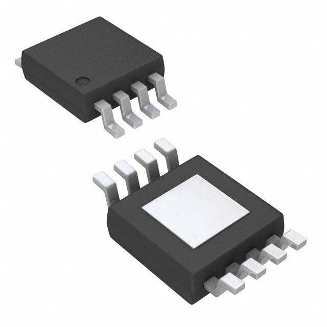
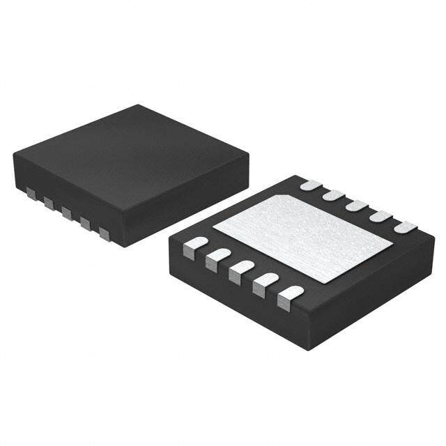
Micrel, Inc. MIC2202 Package Information 10-Pin MSOP (MM) 10-Pin MFL® (ML) March 2007 18 M9999-031907
Micrel, Inc. MIC2202 MICREL, INC. 2180 FORTUNE DRIVE SAN JOSE, CA 95131 USA TEL +1 (408) 944-0800 FAX +1 (408) 474-1000 WEB http://www.micrel.com The information furnished by Micrel in this data sheet is believed to be accurate and reliable. However, no responsibility is assumed by Micrel for its use. Micrel reserves the right to change circuitry and specifications at any time without notification to the customer. Micrel Products are not designed or authorized for use as components in life support appliances, devices or systems where malfunction of a product can reasonably be expected to result in personal injury. Life support devices or systems aredevices or systems that (a) are intended for surgical implant into the body or (b) support or sustain life, and whose failure to perform can be reasonably expected to result in a significant injury to the user. A Purchaser’s use or sale of Micrel Products for use in life support appliances, devices or systems is a Purchaser’s own risk and Purchaser agrees to fully indemnify Micrel for any damages resulting from such use or sale. © 2004 Micrel, Incorporated. March 2007 19 M9999-031907